Self-Assembled Monolayers of Thiolates on Metals as - Whitesides ...
Self-Assembled Monolayers of Thiolates on Metals as - Whitesides ...
Self-Assembled Monolayers of Thiolates on Metals as - Whitesides ...

You also want an ePaper? Increase the reach of your titles
YUMPU automatically turns print PDFs into web optimized ePapers that Google loves.
1134 Chemical Reviews, 2005, Vol. 105, No. 4 Love et al.<br />
<strong>on</strong> surfaces is physical transfer <str<strong>on</strong>g>of</str<strong>on</strong>g> the molecular<br />
comp<strong>on</strong>ents <str<strong>on</strong>g>of</str<strong>on</strong>g> a SAM to the substrate in an imposed<br />
pattern. Microc<strong>on</strong>tact printing (µCP, secti<strong>on</strong> 7.1) and<br />
scanning probe lithography are examples <str<strong>on</strong>g>of</str<strong>on</strong>g> methods<br />
that use this principle. (There are many variati<strong>on</strong>s<br />
<str<strong>on</strong>g>of</str<strong>on</strong>g> scanning probe lithographies for patterning SAMs<br />
that deposit molecules from the tip to the substrate<br />
or that scratch patterns into preformed SAMs. 493 A<br />
number <str<strong>on</strong>g>of</str<strong>on</strong>g> recent reviews address these topics explicitly,<br />
and the topic is not covered in this review.<br />
132,133,362 ) A key difference between µCP and<br />
scanning probe methods is that µCP can generate<br />
many features simultaneously <strong>on</strong> the surface in a<br />
single step, where<strong>as</strong> scanning probes are serial<br />
techniques that <strong>on</strong>ly write <strong>on</strong>e feature at a time. A<br />
disadvantage <str<strong>on</strong>g>of</str<strong>on</strong>g> the probe methods, therefore, is that<br />
they require l<strong>on</strong>g times (minutes to hours per cm 2 )<br />
to write patterns; new technologies for arrays <str<strong>on</strong>g>of</str<strong>on</strong>g><br />
independent scanning probes may improve the practicality<br />
<str<strong>on</strong>g>of</str<strong>on</strong>g> these methods for prototyping structures. 494<br />
Another strategy for generating in-plane patterns<br />
<str<strong>on</strong>g>of</str<strong>on</strong>g> SAMs relies <strong>on</strong> damage to a preformed SAM; an<br />
energetic beam <str<strong>on</strong>g>of</str<strong>on</strong>g> phot<strong>on</strong>s, electr<strong>on</strong>s, or atoms, or<br />
mechanical scratching 213 can cause either chemical<br />
or physical damage to the SAM. Yet another strategy<br />
uses the compositi<strong>on</strong> or topography <str<strong>on</strong>g>of</str<strong>on</strong>g> the substrate<br />
itself to determine the defect sites in the SAM. Both<br />
<str<strong>on</strong>g>of</str<strong>on</strong>g> these strategies may be combined with methods<br />
for exchanging SAMs to replace the damaged regi<strong>on</strong>s<br />
with a SAM presenting different functi<strong>on</strong>al groups.<br />
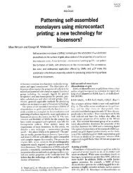
7.1. Microc<strong>on</strong>tact Printing<br />
Microc<strong>on</strong>tact printing is a method for patterning<br />
SAMs <strong>on</strong> surfaces that is operati<strong>on</strong>ally analogous to<br />
printing ink with a rubber stamp <strong>on</strong> paper: SAMs<br />
form in the regi<strong>on</strong>s <str<strong>on</strong>g>of</str<strong>on</strong>g> c<strong>on</strong>tact between a topographically<br />
patterned el<strong>as</strong>tomeric stamp, wetted with (or<br />
c<strong>on</strong>taining dissolved) reactive chemical ‘ink’ c<strong>on</strong>sisting<br />
<str<strong>on</strong>g>of</str<strong>on</strong>g> n-alkanethiols (or other molecules that form<br />
SAMs), and the bare surface <str<strong>on</strong>g>of</str<strong>on</strong>g> a metal, metal oxide,<br />
or semic<strong>on</strong>ductor (Figure 12). 130 When forming patterned<br />
SAMs <str<strong>on</strong>g>of</str<strong>on</strong>g> n-alkanethiolates <strong>on</strong> gold, the stamp<br />
usually is left in c<strong>on</strong>tact with the surface for a few<br />
sec<strong>on</strong>ds (5-10 s) before it is removed. The lateral<br />
dimensi<strong>on</strong>s <str<strong>on</strong>g>of</str<strong>on</strong>g> the SAMs formed depend <strong>on</strong> the<br />
dimensi<strong>on</strong>s <str<strong>on</strong>g>of</str<strong>on</strong>g> relief features <strong>on</strong> the stamp used for<br />
printing; the size <str<strong>on</strong>g>of</str<strong>on</strong>g> the stamp determines the total<br />
area over which the pattern is formed. Typical<br />
patterns generated by µCP cover are<strong>as</strong> <str<strong>on</strong>g>of</str<strong>on</strong>g> 0.1-100<br />
cm2 with critical in-plane dimensi<strong>on</strong>s <str<strong>on</strong>g>of</str<strong>on</strong>g> ∼50 nm to<br />
1000 µm. If required, another SAM can be generated<br />
in the bare regi<strong>on</strong>s <str<strong>on</strong>g>of</str<strong>on</strong>g> the surface that remain after<br />
removing the stamp by immersi<strong>on</strong> <str<strong>on</strong>g>of</str<strong>on</strong>g> the substrate<br />
in a soluti<strong>on</strong> c<strong>on</strong>taining another thiol for a few<br />
minutes (∼1-10 min) or applicati<strong>on</strong> <str<strong>on</strong>g>of</str<strong>on</strong>g> a sec<strong>on</strong>d<br />
stamp wetted with another thiol.<br />
7.1.1. Compositi<strong>on</strong> <str<strong>on</strong>g>of</str<strong>on</strong>g> Topographically Patterned Stamps<br />
The most comm<strong>on</strong> material used for the stamp in<br />
µCP is poly(dimethylsiloxane) (PDMS). PDMS is a<br />
n<strong>on</strong>toxic, commercially available silic<strong>on</strong>e rubber. It<br />
is well-suited for forming stamps because it is el<strong>as</strong>tomeric<br />
(Young’s modulus ≈ 1.8 MPa) and h<strong>as</strong> a low<br />
surface energy (γ ) 21.6 dyn/cm2 ). 495,496 The low<br />
Figure 12. (a) Schematic illustrati<strong>on</strong> depicting the applicati<strong>on</strong><br />
<str<strong>on</strong>g>of</str<strong>on</strong>g> a PDMS stamp c<strong>on</strong>taining thiols to a polycrystalline<br />
metal film. The primary mechanisms <str<strong>on</strong>g>of</str<strong>on</strong>g> m<strong>as</strong>s<br />
transport from the stamp to the surface are shown. The<br />
grayscale gradient approximates the c<strong>on</strong>centrati<strong>on</strong> <str<strong>on</strong>g>of</str<strong>on</strong>g> thiols<br />
adsorbed in the stamp itself. (b) Magnified schematic view<br />
that illustrates the variety <str<strong>on</strong>g>of</str<strong>on</strong>g> structural arrangements<br />
found in SAMs prepared by µCP when the stamp is wetted<br />
with a 1-10 mM soluti<strong>on</strong> and applied to the substrate for<br />
1-10 s.<br />
surface energy makes it e<strong>as</strong>y to remove the stamp<br />
from most surfaces and makes the surface relatively<br />
resistant to c<strong>on</strong>taminati<strong>on</strong> by adsorpti<strong>on</strong> <str<strong>on</strong>g>of</str<strong>on</strong>g> organic<br />
vapors and dust particles. The flexibility <str<strong>on</strong>g>of</str<strong>on</strong>g> the stamp<br />
also allows c<strong>on</strong>formal, that is, molecular level or van<br />
der Waals, c<strong>on</strong>tact between the stamp and substrate;<br />
it is thus critical to molecular-scale printing. This<br />
flexibility also makes it possible to print <strong>on</strong> curved<br />
(n<strong>on</strong>planar) substrates. Another advantage <str<strong>on</strong>g>of</str<strong>on</strong>g> PDMS<br />
is that it is compatible with a wide variety <str<strong>on</strong>g>of</str<strong>on</strong>g> organic<br />
and organometallic molecules because it is unreactive<br />
toward most chemicals; it is, however, swollen by a<br />
number <str<strong>on</strong>g>of</str<strong>on</strong>g> n<strong>on</strong>polar organic solvents. 497<br />
The stamps are formed by c<strong>as</strong>ting a PDMS prepolymer<br />
(a viscous liquid) against a rigid substrate<br />
patterned in reliefsthe ‘m<strong>as</strong>ter’. Fabricati<strong>on</strong> methods<br />
typically used to produce m<strong>as</strong>ters include photolithography,<br />
micromachining, or anisotropic chemical<br />
etching. 498 Commercially available micro- and nanostructured<br />
elements, such <strong>as</strong> diffracti<strong>on</strong> gratings, also<br />
are practical structures to use <strong>as</strong> m<strong>as</strong>ters. Because<br />
the pattern transfer element is formed by molding,<br />
the size <str<strong>on</strong>g>of</str<strong>on</strong>g> the molecular precursors for the crosslinked<br />
polymer determines, in principle, the limitati<strong>on</strong>s<br />
<strong>on</strong> the minimum dimensi<strong>on</strong>s <str<strong>on</strong>g>of</str<strong>on</strong>g> the features<br />
replicated in the stamp. The smallest features that<br />
have been replicated to date by molding are approximately<br />
1.5 nm; these features are defined in the<br />
directi<strong>on</strong> normal to the surface <str<strong>on</strong>g>of</str<strong>on</strong>g> the stamp. 499<br />
Sylgard 184 is the most comm<strong>on</strong> formulati<strong>on</strong> <str<strong>on</strong>g>of</str<strong>on</strong>g><br />
PDMS used for forming stamps because it is commercially<br />
available, inexpensive, and e<strong>as</strong>y to use. 500