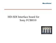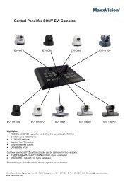
SONY FCB H11 and FCB EH4300 SDI Interface ... - MaxxVision
SONY FCB H11 and FCB EH4300 SDI Interface ... - MaxxVision
SONY FCB H11 and FCB EH4300 SDI Interface ... - MaxxVision

Create successful ePaper yourself
Turn your PDF publications into a flip-book with our unique Google optimized e-Paper software.
<strong>SONY</strong> <strong>FCB</strong> <strong>H11</strong> <strong>and</strong> <strong>FCB</strong> <strong>EH4300</strong> <strong>SDI</strong><br />
<strong>Interface</strong> module<br />
Technical manual
Content<br />
1 Presentaon ......................................................................................................................................... 3<br />
1.1 Synoptic ........................................................................................................................................3<br />
1.2 Caracteristics .................................................................................................................................4<br />
1.2 1 HD Video Input ......................................................................................................................4<br />
1.2.2 Analog SD input .....................................................................................................................4<br />
1.2.3 <strong>SDI</strong> output ..............................................................................................................................4<br />
1.2.4 HD Analog output ..................................................................................................................4<br />
1.2.5 Serial RS232 Communication. ...............................................................................................4<br />
1.2.6 Power .....................................................................................................................................4<br />
2 Connecons .......................................................................................................................................... 5<br />
2.1 With <strong>SONY</strong> <strong>FCB</strong>-<strong>H11</strong> ..................................................................................................................5<br />
2.2 With <strong>SONY</strong> <strong>FCB</strong>-<strong>EH4300</strong> ............................................................................................................6<br />
2.3 Camera connection ........................................................................................................................6<br />
2.4 Pin assignments of connectors) .....................................................................................................6<br />
2.4.1 Power(J6) ...............................................................................................................................6<br />
2.4.2FFC to camera (J3) ..................................................................................................................7<br />
2.4.3 LVDS from <strong>FCB</strong>-<strong>H11</strong> camera (J2) ........................................................................................7<br />
2.4.4 LVDS from <strong>FCB</strong>-<strong>EH4300</strong> camera (J5) ..................................................................................8<br />
2.4.5 Analog video ouput (J7) .........................................................................................................8<br />
2.4.6 Analog SD Y/C (J4) <strong>and</strong> VBS composite (J10) .....................................................................9<br />
3 Signalizaon <strong>and</strong> conguraon ............................................................................................................ 9<br />
3.1 Signaling LED ...............................................................................................................................10<br />
3.2 Video format configuration micro switches. .................................................................................10<br />
3.3 Solder jumpers Y/C, PS1 <strong>and</strong> PS2 ................................................................................................11<br />
3.4 Mode SD-<strong>SDI</strong> avec le bloc <strong>FCB</strong>-<strong>EH4300</strong> ....................................................................................11<br />
3.5 Solder jumpers RS232, PS3 <strong>and</strong> PS4 ............................................................................................12<br />
4 Mechanical Diagram ............................................................................................................................. 12<br />
4.1 Mounting of the interface board ....................................................................................................13<br />
4.2 Connections for <strong>FCB</strong> <strong>H11</strong> .............................................................................................................13<br />
4.3 Connections for <strong>FCB</strong> EH 4300 .....................................................................................................13
Technical manual 3<br />
1 Presenta on<br />
This interface provides an <strong>SDI</strong> output to <strong>SONY</strong> <strong>FCB</strong>-<strong>H11</strong> <strong>and</strong> Sony <strong>FCB</strong>-<strong>EH4300</strong> cameras.<br />
It also provides access to analog video outputs of the camera.<br />
It controls the video format of the camera using built in switches <strong>and</strong> converts RS232 to TTL levels<br />
1.1 Synop c<br />
C<br />
A<br />
M<br />
E<br />
R<br />
A<br />
5 x<br />
Y/C<br />
SD<br />
FPGA<br />
TTL<br />
6 to 12VDC<br />
RS232 /<br />
Power<br />
supply<br />
8 bits<br />
CAN<br />
Main func ons:<br />
Serializa on <strong>and</strong> adapta on of the st<strong>and</strong>ard <strong>SDI</strong> signal.<br />
At startup, reading the video format of the camera, congura on according switches (RS232<br />
VISCA protocol).<br />
Conversion of RS232/TTL level for external control.<br />
Camera power ( 6 to 12 V external) <strong>and</strong> the board voltages : 1.2V, 1.8 V, <strong>and</strong> 3.3 V<br />
HD mode<br />
Receiving LVDS signals (FPGA)<br />
Interpola on (in 1080i for the <strong>FCB</strong>-<strong>H11</strong> block only) (FPGA)<br />
Forma ng 16-bit BT656 (FPGA)<br />
SD mode<br />
Analog/digital conversion <strong>and</strong> decoding<br />
Forma ng 16 bits BT656 ( FPGA)<br />
CLK<br />
RS232<br />
+ 3,3<br />
+ 1,8<br />
+ 1,2<br />
8 bits<br />
CL<br />
uC<br />
Serialiser<br />
<strong>SDI</strong><br />
<strong>SDI</strong>
Technical manual 4<br />
1.2 Caracteris cs<br />
1.2 1 HD Video Input<br />
<strong>FCB</strong>-<strong>H11</strong> <strong>FCB</strong>-<strong>EH4300</strong><br />
Connector KEL SSL00-10L3 KEL USL00-30L3<br />
Cable assembly SSL-20-10SSB-009-B USL20-30SS-005-C<br />
Signals 4 x LVDS pairs + clock 4 x LVDS pairs + clock<br />
Type Y, Cb, Cr 8 bit + HVF Y, Cb/Cr 8 bit + HVF<br />
Formats - 1080i50 <strong>and</strong> 59,94 (H= 55,68MHz)<br />
1440 pixels per line<br />
- 720p50 <strong>and</strong> 59,94 (H= 74,25MHz)<br />
-1080i50 <strong>and</strong> 60 (H= 74,25MHz)<br />
- 1080p25 <strong>and</strong> 30 (H= 74,25MHz)<br />
- 720p50* <strong>and</strong> 60 (H= 74,25MHz)<br />
- 720p25* <strong>and</strong> 30* (H= ?)<br />
1.2.2 Analog SD input<br />
<strong>FCB</strong>-<strong>H11</strong> <strong>FCB</strong>-<strong>EH4300</strong><br />
Connector KYOCERA 04 6240 0240 KEL USL00-30L3<br />
Signals Y/C Composite<br />
Formats - PAL <strong>and</strong> NTSC (crop 4/3) - PAL <strong>and</strong> NTSC (16/9)<br />
1.2.3 <strong>SDI</strong> output<br />
BNC or SMB Connector<br />
8 bits <strong>SDI</strong> Signal depending on SMPTE 259M or 292M st<strong>and</strong>ards, 800mVcc, 75ohm impedance<br />
Frequency : HD = 1,485Gbit/s, SD = 270Mbit/s<br />
Formats :<br />
<strong>FCB</strong>-<strong>H11</strong> : 1080i50, 1080i59.94, 720p50, 72p59.94, PAL, NTSC<br />
<strong>FCB</strong>-<strong>EH4300</strong> : 1080i50, 1080i560, 1080p25, 1080p30, 720p50*, 72p60, 720p25*, 720p30*, PAL, NTSC<br />
(* not ac ve in this version)<br />
1.2.4 HD Analog output<br />
Molex 1,25m: 53398-1071<br />
HD : format YPbPr.<br />
SD : Y/C <strong>and</strong> composite.<br />
1.2.5 Serial RS232 Communica on.<br />
Molex 1,25mm , 53398-1071<br />
RS232 level or TTL level.<br />
1.2.6 Power<br />
Molex 1.25, 53398-0271<br />
Power : +6 to 12VDC, 1,5W ( interface board only)
Technical manual 5<br />
2 Connec ons<br />
2.1 With <strong>SONY</strong> <strong>FCB</strong>-<strong>H11</strong><br />
YPbPr <strong>and</strong> RS232<br />
FFC<br />
Camera connection<br />
Power 6 to 12V DC<br />
SD VBS output<br />
SD Y/C output<br />
<strong>SDI</strong> output<br />
LVDS <strong>FCB</strong> <strong>H11</strong> connection
2.2 With <strong>SONY</strong> <strong>FCB</strong>-<strong>EH4300</strong><br />
FFC camera connection **<br />
Technical manual 6<br />
2.3 Camera connecon<br />
LVSDS cable assembly: cable 30 ways KEL type USL20-30SS-xxx-C<br />
FFC cable: 24 ways 0,5mm<br />
** For this EH 4300 camera, the connecon with FFC is not necessary because the LVDS link bring<br />
LVDS signals, power, analog HD <strong>and</strong> SD analog video , <strong>and</strong> RS232 comm<strong>and</strong>.<br />
2.4 Pin assignments of connectors)<br />
2.4.1 Power(J6)<br />
YPbPr <strong>and</strong> RS232<br />
LVDS<br />
Camera<br />
connection<br />
Connector MOLEX 53398-0271<br />
Power<br />
6 to 12V DC<br />
+V 0V<br />
1 2<br />
SD VBS output<br />
SD Y/C output<br />
<strong>SDI</strong> output
Technical manual 7<br />
2.4.2FFC to camera (J3)<br />
KYOCERA 04 6240 0240<br />
2.4.3 LVDS from <strong>FCB</strong>-<strong>H11</strong> camera (J2)<br />
Connector: KEL SSL00-10L3<br />
Cable assembly SSL-20-10SSB-009-B for <strong>FCB</strong> <strong>H11</strong><br />
1 0V-GND<br />
2 +V<br />
3 0V-GND<br />
4 +V<br />
5 +V<br />
6 +V<br />
7 +V<br />
8 0V-GND<br />
9 Pr<br />
10 0V-GND<br />
11 Pb<br />
12 0V-GND<br />
13 Y<br />
14 0V-GND<br />
15 VBS<br />
16 0V-GND<br />
17 C<br />
18 0V-GND<br />
19 Y<br />
20 0V-GND<br />
21 Reset In<br />
22 RxD ( TTL camera input)<br />
23 TxD (TTL camera output)<br />
24 0V-GND<br />
10 TX3+<br />
9 TX3-<br />
8 TXCLKOUT+<br />
7 TXCLKOUT-<br />
6 TX2+<br />
5 TX2-<br />
4 TX1+<br />
3 TX1-<br />
2 TX0+<br />
1 TX0-
Technical manual 8<br />
2.4.4 LVDS from <strong>FCB</strong>-<strong>EH4300</strong> camera (J5)<br />
Connector KEL USL00-30L3<br />
Cable assembly USL-20-30SS-005C for <strong>FCB</strong> <strong>EH4300</strong><br />
2.4.5 Analog video ouput (J7)<br />
Connector MOLEX 53398-1071<br />
TxD: interface module output to PC SUBD9 pin2<br />
RxD: interface module input to PC SUBD9 pin3<br />
You can set RS232 or TTL depending<br />
solder jumpers<br />
30 Pr<br />
29 Pb<br />
28 Y<br />
27 VBS<br />
26 C<br />
25 Y<br />
24 0V-GND<br />
23 0V-GND<br />
22 0V-GND<br />
21 0V-GND<br />
20 0V-GND<br />
19 0V-GND<br />
18 +V<br />
17 +V<br />
16 +V<br />
15 +V<br />
14 +V<br />
13 RxD ( TTL camera input)<br />
12 TxD ( TTL camera output)<br />
11 0V-GND<br />
10 TX0-<br />
9 TX0+<br />
8 TX1-<br />
7 TX1+<br />
6 TX2-<br />
5 TX2+<br />
4 TXCLKOUT-<br />
3 TXCLKOUT+<br />
2 TX3-<br />
1 TX3+<br />
Y Gnd Pb Gnd Pr Gnd TxD RxD Gnd<br />
1 2 3 4 5 6 7 8 9 10
Technical manual 9<br />
2.4.6 Analog SD Y/C (J4) <strong>and</strong> VBS composite (J10)<br />
Wires must be soldered on the PCB through 2,54mm, 3 holes for YC <strong>and</strong> 2 holes for VBS.<br />
3 Signalizaon <strong>and</strong> conguraon<br />
Y/C Solder jumpers<br />
RS232/TTL solder jumpers<br />
VBS Gnd<br />
1 2<br />
Y Gnd C<br />
1 2 3<br />
Signalizaon LED<br />
Video format<br />
microswitches
Technical manual 10<br />
3.1 Signaling LED<br />
In order to visualize informaon, the LED is eming a lot of shorts blinks.<br />
The number of blinks indicates the status of the module.<br />
1 blink each 2 seconds: module rmware boot.<br />
2 blinks each 2 seconds: decoder inializaon OK.<br />
3 blinks each 2 seconds: FPGA loading OK.<br />
4 blinks each 2 seconds: VISCA dialog with camera OK<br />
5 blinks each 2 seconds: Camera video format conguraon OK<br />
6 blinks each 2 seconds: FPGA video conguraon OK<br />
7 blinks each 2 seconds: dem<strong>and</strong> of video format modicaon by micro switch<br />
3.2 Video format conguraon micro switches.<br />
In the "External" mode, the interface module does not change the format of the video camera.<br />
In other modes, the board checks, at the camera power on if the camera video format corresponds to<br />
the switches, otherwise it sends a VISCA comm<strong>and</strong> to change format.<br />
The camera must be powered o <strong>and</strong> powered on TWICE to take the new format into account.<br />
1 2 3 4 <strong>FCB</strong>-<strong>H11</strong> video format <strong>FCB</strong>-<strong>EH4300</strong> video format<br />
OFF OFF OFF OFF Externe Externe<br />
ON OFF OFF OFF 1080p30<br />
OFF ON OFF OFF 1080p25<br />
ON ON OFF OFF 1080i59,94 1080i60<br />
OFF OFF ON OFF 1080i50 1080i50<br />
ON OFF ON OFF 720p59,94 720p60<br />
OFF ON ON OFF 720p50 720p50*<br />
ON ON ON OFF 720p30*<br />
OFF OFF OFF ON 720p25*<br />
ON OFF OFF ON NTSC NTSC<br />
OFF ON OFF ON PAL PAL<br />
ON ON OFF ON
Technical manual 11<br />
OFF OFF ON ON<br />
ON OFF ON ON<br />
OFF ON ON ON<br />
ON ON ON ON<br />
3.3 Solder jumpers Y/C, PS1 <strong>and</strong> PS2<br />
When the solder jumpers are completed, the Y/C signals from the camera are sent to the decoder of<br />
the module (75 Ohms resistor ere loaded ) <strong>and</strong> to the J4 connector.<br />
SD-<strong>SDI</strong> output is funconal <strong>and</strong> Y / C signals are available for a high impedance input.<br />
Solder jumper<br />
If the Y / C signals must be used in analog externally with loads of 75 ohms, remove the solder<br />
jumpers to avoid the double75 ohms load. In this case the output SD-<strong>SDI</strong> does not work anymore.<br />
3.4 SD-<strong>SDI</strong> mode with <strong>FCB</strong>-<strong>EH4300</strong><br />
This camera does not output SD Y/C video signal. It is necessary to realize a solder jump between<br />
CVBS-Y to get a SD <strong>SDI</strong> output from the interface board.<br />
This connecon can be done by soldering hole No 1 from J4 <strong>and</strong> J10.
Technical manual 12<br />
3.5 Solder jumpers RS232, PS3 <strong>and</strong> PS4<br />
These solder jumpers allow to select TTL or RS232 level of external serial communicaon.<br />
RS232 level: signals are converted from RS232 level to TTTL level before connecng to the camera<br />
B B<br />
B B<br />
TTL Level: Communicaon signals are connected to the camera through the FPGA. The RS232<br />
converter is bypassed. This posion is visualized by « B »leer wrien on the Printed Circuit Board.<br />
4 Mechanical Diagram<br />
3 x Diam 2.5<br />
45 mm<br />
2.6 mm<br />
26 mm<br />
2 mm<br />
48 mm
Technical manual 13<br />
4.1 Mounting of the interface board<br />
4 x M2 x 4<br />
4.2 Connections for <strong>FCB</strong> <strong>H11</strong><br />
1<br />
4.3 Connections for <strong>FCB</strong> EH 4300<br />
1<br />
3 x M2 x 6<br />
6 x M2 x 4<br />
Holes for <strong>FCB</strong> <strong>H11</strong><br />
Holes for <strong>FCB</strong> EH 4300<br />
2