LCD TV SERVICE MANUAL - TV & Monitor Service Manual Database
LCD TV SERVICE MANUAL - TV & Monitor Service Manual Database
LCD TV SERVICE MANUAL - TV & Monitor Service Manual Database

You also want an ePaper? Increase the reach of your titles
YUMPU automatically turns print PDFs into web optimized ePapers that Google loves.
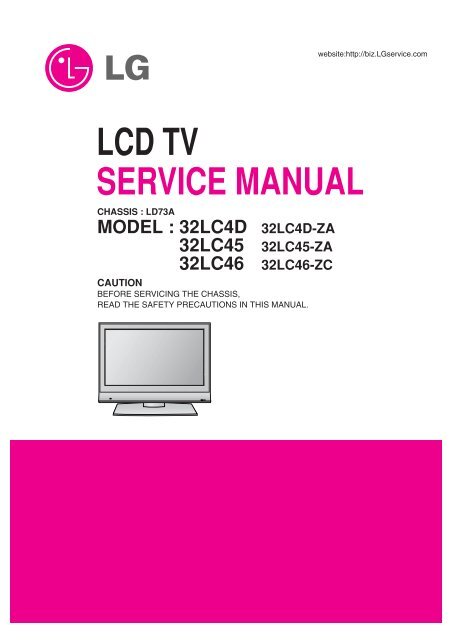
<strong>LCD</strong> <strong>TV</strong><br />
<strong>SERVICE</strong> <strong>MANUAL</strong><br />
CHASSIS : LD73A<br />
MODEL : 32LC4D 32LC4D-ZA<br />
MODEL : 32LC45 32LC45-ZA<br />
MODEL : 32LC46 32LC46-ZC<br />
CAUTION<br />
BEFORE SERVICING THE CHASSIS,<br />
READ THE SAFETY PRECAUTIONS IN THIS <strong>MANUAL</strong>.<br />
R<br />
website:http://biz.LGservice.com
CONTENTS<br />
CONTENTS .............................................................................................. 2<br />
PRODUCT SAFETY ..................................................................................3<br />
SPECIFICATION ........................................................................................6<br />
ADJUSTMENT INSTRUCTION .................................................................9<br />
TROUBLE SHOOTING ............................................................................14<br />
BLOCK DIAGRAM...................................................................................22<br />
EXPLODED VIEW .................................................................................. 24<br />
REPLACEMENT PARTS LIST ............................................................... 26<br />
SVC. SHEET ...............................................................................................<br />
- 2 -
SAFETY PRECAUTIONS<br />
Many electrical and mechanical parts in this chassis have special safety-related characteristics. These parts are identified by in the<br />
Schematic Diagram and Replacement Parts List.<br />
It is essential that these special safety parts should be replaced with the same components as recommended in this manual to prevent<br />
Shock, Fire, or other Hazards.<br />
Do not modify the original design without permission of manufacturer.<br />
General Guidance<br />
An isolation Transformer should always be used during the<br />
servicing of a receiver whose chassis is not isolated from the AC<br />
power line. Use a transformer of adequate power rating as this<br />
protects the technician from accidents resulting in personal injury<br />
from electrical shocks.<br />
It will also protect the receiver and it's components from being<br />
damaged by accidental shorts of the circuitry that may be<br />
inadvertently introduced during the service operation.<br />
If any fuse (or Fusible Resistor) in this <strong>TV</strong> receiver is blown,<br />
replace it with the specified.<br />
When replacing a high wattage resistor (Oxide Metal Film Resistor,<br />
over 1W), keep the resistor 10mm away from PCB.<br />
Keep wires away from high voltage or high temperature parts.<br />
Before returning the receiver to the customer,<br />
always perform an AC leakage current check on the exposed<br />
metallic parts of the cabinet, such as antennas, terminals, etc., to<br />
be sure the set is safe to operate without damage of electrical<br />
shock.<br />
Leakage Current Cold Check(Antenna Cold Check)<br />
With the instrument AC plug removed from AC source, connect an<br />
electrical jumper across the two AC plug prongs. Place the AC<br />
switch in the on position, connect one lead of ohm-meter to the AC<br />
plug prongs tied together and touch other ohm-meter lead in turn to<br />
each exposed metallic parts such as antenna terminals, phone<br />
jacks, etc.<br />
If the exposed metallic part has a return path to the chassis, the<br />
measured resistance should be between 1MΩ and 5.2MΩ.<br />
When the exposed metal has no return path to the chassis the<br />
reading must be infinite.<br />
An other abnormality exists that must be corrected before the<br />
receiver is returned to the customer.<br />
IMPORTANT SAFETY NOTICE<br />
- 3 -<br />
Leakage Current Hot Check (See below Figure)<br />
Plug the AC cord directly into the AC outlet.<br />
Do not use a line Isolation Transformer during this check.<br />
Connect 1.5K/10watt resistor in parallel with a 0.15uF capacitor<br />
between a known good earth ground (Water Pipe, Conduit, etc.)<br />
and the exposed metallic parts.<br />
Measure the AC voltage across the resistor using AC voltmeter<br />
with 1000 ohms/volt or more sensitivity.<br />
Reverse plug the AC cord into the AC outlet and repeat AC voltage<br />
measurements for each exposed metallic part. Any voltage<br />
measured must not exceed 0.75 volt RMS which is corresponds to<br />
0.5mA.<br />
In case any measurement is out of the limits specified, there is<br />
possibility of shock hazard and the set must be checked and<br />
repaired before it is returned to the customer.<br />
Leakage Current Hot Check circuit<br />
To Instrument’s<br />
exposed<br />
METALLIC PARTS<br />
AC Volt-meter<br />
0.15uF<br />
1.5 Kohm/10W<br />
Good Earth Ground<br />
such as WATER PIPE,<br />
CONDUIT etc.
CAUTION: Before servicing receivers covered by this service<br />
manual and its supplements and addenda, read and follow the<br />
SAFETY PRECAUTIONS on page 3 of this publication.<br />
NOTE: If unforeseen circumstances create conflict between the<br />
following servicing precautions and any of the safety precautions on<br />
page 3 of this publication, always follow the safety precautions.<br />
Remember: Safety First.<br />
General Servicing Precautions<br />
1. Always unplug the receiver AC power cord from the AC power<br />
source before;<br />
a. Removing or reinstalling any component, circuit board<br />
module or any other receiver assembly.<br />
b. Disconnecting or reconnecting any receiver electrical plug or<br />
other electrical connection.<br />
c. Connecting a test substitute in parallel with an electrolytic<br />
capacitor in the receiver.<br />
CAUTION: A wrong part substitution or incorrect polarity<br />
installation of electrolytic capacitors may result in an<br />
explosion hazard.<br />
2. Test high voltage only by measuring it with an appropriate high<br />
voltage meter or other voltage measuring device (DVM,<br />
FE<strong>TV</strong>OM, etc) equipped with a suitable high voltage probe.<br />
Do not test high voltage by "drawing an arc".<br />
3. Do not spray chemicals on or near this receiver or any of its<br />
assemblies.<br />
4. Unless specified otherwise in this service manual, clean<br />
electrical contacts only by applying the following mixture to the<br />
contacts with a pipe cleaner, cotton-tipped stick or comparable<br />
non-abrasive applicator; 10% (by volume) Acetone and 90% (by<br />
volume) isopropyl alcohol (90%-99% strength)<br />
CAUTION: This is a flammable mixture.<br />
Unless specified otherwise in this service manual, lubrication of<br />
contacts in not required.<br />
5. Do not defeat any plug/socket B+ voltage interlocks with which<br />
receivers covered by this service manual might be equipped.<br />
6. Do not apply AC power to this instrument and/or any of its<br />
electrical assemblies unless all solid-state device heat sinks are<br />
correctly installed.<br />
7. Always connect the test receiver ground lead to the receiver<br />
chassis ground before connecting the test receiver positive<br />
lead.<br />
Always remove the test receiver ground lead last.<br />
8. Use with this receiver only the test fixtures specified in this<br />
service manual.<br />
CAUTION: Do not connect the test fixture ground strap to any<br />
heat sink in this receiver.<br />
Electrostatically Sensitive (ES) Devices<br />
Some semiconductor (solid-state) devices can be damaged easily<br />
by static electricity. Such components commonly are called<br />
Electrostatically Sensitive (ES) Devices. Examples of typical ES<br />
devices are integrated circuits and some field-effect transistors and<br />
semiconductor "chip" components. The following techniques<br />
should be used to help reduce the incidence of component<br />
damage caused by static by static electricity.<br />
1. Immediately before handling any semiconductor component or<br />
semiconductor-equipped assembly, drain off any electrostatic<br />
charge on your body by touching a known earth ground.<br />
Alternatively, obtain and wear a commercially available<br />
discharging wrist strap device, which should be removed to<br />
prevent potential shock reasons prior to applying power to the<br />
SERVICING PRECAUTIONS<br />
- 4 -<br />
unit under test.<br />
2. After removing an electrical assembly equipped with ES<br />
devices, place the assembly on a conductive surface such as<br />
aluminum foil, to prevent electrostatic charge buildup or<br />
exposure of the assembly.<br />
3. Use only a grounded-tip soldering iron to solder or unsolder ES<br />
devices.<br />
4. Use only an anti-static type solder removal device. Some solder<br />
removal devices not classified as "anti-static" can generate<br />
electrical charges sufficient to damage ES devices.<br />
5. Do not use freon-propelled chemicals. These can generate<br />
electrical charges sufficient to damage ES devices.<br />
6. Do not remove a replacement ES device from its protective<br />
package until immediately before you are ready to install it.<br />
(Most replacement ES devices are packaged with leads<br />
electrically shorted together by conductive foam, aluminum foil<br />
or comparable conductive material).<br />
7. Immediately before removing the protective material from the<br />
leads of a replacement ES device, touch the protective material<br />
to the chassis or circuit assembly into which the device will be<br />
installed.<br />
CAUTION: Be sure no power is applied to the chassis or circuit,<br />
and observe all other safety precautions.<br />
8. Minimize bodily motions when handling unpackaged<br />
replacement ES devices. (Otherwise harmless motion such as<br />
the brushing together of your clothes fabric or the lifting of your<br />
foot from a carpeted floor can generate static electricity<br />
sufficient to damage an ES device.)<br />
General Soldering Guidelines<br />
1. Use a grounded-tip, low-wattage soldering iron and appropriate<br />
tip size and shape that will maintain tip temperature within the<br />
range or 500°F to 600°F.<br />
2. Use an appropriate gauge of RMA resin-core solder composed<br />
of 60 parts tin/40 parts lead.<br />
3. Keep the soldering iron tip clean and well tinned.<br />
4. Thoroughly clean the surfaces to be soldered. Use a mall wirebristle<br />
(0.5 inch, or 1.25cm) brush with a metal handle.<br />
Do not use freon-propelled spray-on cleaners.<br />
5. Use the following unsoldering technique<br />
a. Allow the soldering iron tip to reach normal temperature.<br />
(500°F to 600°F)<br />
b. Heat the component lead until the solder melts.<br />
c. Quickly draw the melted solder with an anti-static, suctiontype<br />
solder removal device or with solder braid.<br />
CAUTION: Work quickly to avoid overheating the<br />
circuitboard printed foil.<br />
6. Use the following soldering technique.<br />
a. Allow the soldering iron tip to reach a normal temperature<br />
(500°F to 600°F)<br />
b. First, hold the soldering iron tip and solder the strand against<br />
the component lead until the solder melts.<br />
c. Quickly move the soldering iron tip to the junction of the<br />
component lead and the printed circuit foil, and hold it there<br />
only until the solder flows onto and around both the<br />
component lead and the foil.<br />
CAUTION: Work quickly to avoid overheating the circuit<br />
board printed foil.<br />
d. Closely inspect the solder area and remove any excess or<br />
splashed solder with a small wire-bristle brush.
IC Remove/Replacement<br />
Some chassis circuit boards have slotted holes (oblong) through<br />
which the IC leads are inserted and then bent flat against the<br />
circuit foil. When holes are the slotted type, the following technique<br />
should be used to remove and replace the IC. When working with<br />
boards using the familiar round hole, use the standard technique<br />
as outlined in paragraphs 5 and 6 above.<br />
Removal<br />
1. Desolder and straighten each IC lead in one operation by gently<br />
prying up on the lead with the soldering iron tip as the solder<br />
melts.<br />
2. Draw away the melted solder with an anti-static suction-type<br />
solder removal device (or with solder braid) before removing the<br />
IC.<br />
Replacement<br />
1. Carefully insert the replacement IC in the circuit board.<br />
2. Carefully bend each IC lead against the circuit foil pad and<br />
solder it.<br />
3. Clean the soldered areas with a small wire-bristle brush.<br />
(It is not necessary to reapply acrylic coating to the areas).<br />
"Small-Signal" Discrete Transistor<br />
Removal/Replacement<br />
1. Remove the defective transistor by clipping its leads as close as<br />
possible to the component body.<br />
2. Bend into a "U" shape the end of each of three leads remaining<br />
on the circuit board.<br />
3. Bend into a "U" shape the replacement transistor leads.<br />
4. Connect the replacement transistor leads to the corresponding<br />
leads extending from the circuit board and crimp the "U" with<br />
long nose pliers to insure metal to metal contact then solder<br />
each connection.<br />
Power Output, Transistor Device<br />
Removal/Replacement<br />
1. Heat and remove all solder from around the transistor leads.<br />
2. Remove the heat sink mounting screw (if so equipped).<br />
3. Carefully remove the transistor from the heat sink of the circuit<br />
board.<br />
4. Insert new transistor in the circuit board.<br />
5. Solder each transistor lead, and clip off excess lead.<br />
6. Replace heat sink.<br />
Diode Removal/Replacement<br />
1. Remove defective diode by clipping its leads as close as<br />
possible to diode body.<br />
2. Bend the two remaining leads perpendicular y to the circuit<br />
board.<br />
3. Observing diode polarity, wrap each lead of the new diode<br />
around the corresponding lead on the circuit board.<br />
4. Securely crimp each connection and solder it.<br />
5. Inspect (on the circuit board copper side) the solder joints of<br />
the two "original" leads. If they are not shiny, reheat them and if<br />
necessary, apply additional solder.<br />
Fuse and Conventional Resistor<br />
Removal/Replacement<br />
1. Clip each fuse or resistor lead at top of the circuit board hollow<br />
stake.<br />
2. Securely crimp the leads of replacement component around<br />
notch at stake top.<br />
3. Solder the connections.<br />
CAUTION: Maintain original spacing between the replaced<br />
component and adjacent components and the circuit board to<br />
prevent excessive component temperatures.<br />
- 5 -<br />
Circuit Board Foil Repair<br />
Excessive heat applied to the copper foil of any printed circuit<br />
board will weaken the adhesive that bonds the foil to the circuit<br />
board causing the foil to separate from or "lift-off" the board. The<br />
following guidelines and procedures should be followed whenever<br />
this condition is encountered.<br />
At IC Connections<br />
To repair a defective copper pattern at IC connections use the<br />
following procedure to install a jumper wire on the copper pattern<br />
side of the circuit board. (Use this technique only on IC<br />
connections).<br />
1. Carefully remove the damaged copper pattern with a sharp<br />
knife. (Remove only as much copper as absolutely necessary).<br />
2. carefully scratch away the solder resist and acrylic coating (if<br />
used) from the end of the remaining copper pattern.<br />
3. Bend a small "U" in one end of a small gauge jumper wire and<br />
carefully crimp it around the IC pin. Solder the IC connection.<br />
4. Route the jumper wire along the path of the out-away copper<br />
pattern and let it overlap the previously scraped end of the good<br />
copper pattern. Solder the overlapped area and clip off any<br />
excess jumper wire.<br />
At Other Connections<br />
Use the following technique to repair the defective copper pattern<br />
at connections other than IC Pins. This technique involves the<br />
installation of a jumper wire on the component side of the circuit<br />
board.<br />
1. Remove the defective copper pattern with a sharp knife.<br />
Remove at least 1/4 inch of copper, to ensure that a hazardous<br />
condition will not exist if the jumper wire opens.<br />
2. Trace along the copper pattern from both sides of the pattern<br />
break and locate the nearest component that is directly<br />
connected to the affected copper pattern.<br />
3. Connect insulated 20-gauge jumper wire from the lead of the<br />
nearest component on one side of the pattern break to the lead<br />
of the nearest component on the other side.<br />
Carefully crimp and solder the connections.<br />
CAUTION: Be sure the insulated jumper wire is dressed so the<br />
it does not touch components or sharp edges.
SPECIFICATION<br />
NOTE : Specifications and others are subject to change without notice for improvement.<br />
1. General Specification(<strong>TV</strong>)<br />
No Item Specification Remark<br />
1. Video input applicable system PAL-D/K, B/G, I, SECAM<br />
2. Receivable Broadcasting System 1) PAL/SECAM BG EU(PAL Market)<br />
2) PAL/SECAM DK<br />
3) PAL I/I<br />
4) SECAM L/L'<br />
5) DVB-T<br />
3. RF Input Channel VHF : E2 ~ E12 PAL<br />
UHF : E21 ~ E69<br />
CA<strong>TV</strong> : S1 ~ S20<br />
HYPER : S21~ S47<br />
4. Input Voltage 100 - 240~ / 50Hz, 60Hz<br />
5. Market EU<br />
6. Picture Size 32 inch<br />
7. Tuning System FVS 100 program PAL, 200 PR.(Option)<br />
8. Operating Environment 1) Temp : 0 ~ 40 deg<br />
2) Humidity : 10~90 %<br />
9. Storage Environment 3) Temp : -20 ~ 50 deg<br />
4) Humidity : 10~90 %<br />
10. Display <strong>LCD</strong> Module LPL<br />
2. General Specification<br />
No Item Specification Remark<br />
1 Panel 32" TFT WXGA <strong>LCD</strong><br />
2 Frequency range H : 45 ~ 50Khz<br />
V : 47 ~ 63Hz<br />
PC Input<br />
3 Power consumption 26inch ≤ 4.6 W<br />
32inch ≤ 5.54 W<br />
4 <strong>LCD</strong> Module- LPL(32inch) Type Size 32" 760.0 x 450.0 x 42.8(mm) (H)x(V)x(D)<br />
Pixel Pitch 32" 170.25 x 510.75 x RGB(µm)<br />
Pixel Format 1366 horiz. By 768 vert. Pixels<br />
RGB strip arrangement<br />
Coating Hard coating (3H), Anti-glare<br />
reatment of the front polarizer<br />
Back Light 32" 18EEFL<br />
- 6 -
3. Optical Feature(<strong>LCD</strong> Module-LPL)<br />
No Item Specification Min. Typ. Max. Remark<br />
1 Viewing Angle [CR>10] R/L, U/D 178, 178<br />
2 Luminance Luminance(cd/m2) 320 400 32”<br />
Variation 1.3 MAX/MIN<br />
3 Contrast Ratio CR(32") 600 800 All White/All Black<br />
CRD (With)(32") 1200 1600 All White/All Black<br />
4 CIE Color Coordinates White Wx Typ 0.285 Typ LPL(26”)<br />
Wy -0.03 0.293 +0.03<br />
Red Xr 0.640<br />
Yr 0.343<br />
Green Xg 0.280<br />
Yg 0.605<br />
Blue Xb 0.145<br />
Yb 0.065<br />
4. Component Video Input (Y, PB, PR)<br />
No<br />
Resolution H-freq(kHz)<br />
Specification<br />
V-freq(Hz)<br />
1. 720x480 15.73 60.00 SD<strong>TV</strong>, DVD 480i<br />
2. 720x480 15.63 59.94 SD<strong>TV</strong>, DVD 480i<br />
3. 720x480 31.47 59.94 480p<br />
4. 720x576 15.625 50.00 SD<strong>TV</strong>, DVD 625 Line<br />
5. 720x576 31.25 50.00 HD<strong>TV</strong> 576p<br />
6. 1280x720 45.00 50.00 HD<strong>TV</strong> 720p<br />
7. 1280x720 44.96 59.94 HD<strong>TV</strong> 720p<br />
8. 1920x1080 31.25 50.00 HD<strong>TV</strong> 1080i<br />
9. 1920x1080 33.75 60.00 HD<strong>TV</strong> 1080i<br />
10. 1920x1080 33.72 59.94 HD<strong>TV</strong> 1080i<br />
6. RGB PC INPUT Mode Table<br />
No Resolution H-freq(kHz) V-freq.(Hz) Pixel clock(MHz) Proposed<br />
1. 720X400 31.468 70.08 28.321<br />
2. 640X480 31.469 59.94 25.17 VESA<br />
37.684 75.00 31.50<br />
3. 800X600 37.879 60.31 40.00 VESA<br />
46.875 75.00 49.50<br />
4. 832X624 49.725 74.55 57.283<br />
5. 1024X768 48.363 60.00 65.00 VESA(XGA)<br />
56.470 70.00 75.00<br />
60.123 75.029 78.75<br />
6. 1280X768 47.776 59.870 79.50 VESA(WXGA)<br />
7. 1360X768 47.720 59.799 84.75 VESA(WXGA)<br />
8. 1366X768 47.720 59.799 84.75 Supported<br />
9. 1920X1080 67.50 60.00 148.50<br />
- 7 -<br />
Proposed
7. HDMI D<strong>TV</strong> Mode Table<br />
No Resolution H-freq(kHz) V-freq.(Hz) Pixel clock(MHz) Remark Proposed<br />
1. 640X480 31.50 59.94 25.175 SD<strong>TV</strong> 480p 60Hz<br />
2. 640X480 31.50 60 25.20 SD<strong>TV</strong> 480p 60Hz<br />
3. 720X480 31.47 59.94 27.00 SD<strong>TV</strong> 480p 60Hz<br />
4. 720X480 31.47 60 27.027 SD<strong>TV</strong> 480p 60Hz<br />
5. 720X576 31.25 50.00 27.000 SD<strong>TV</strong> 576p 50Hz<br />
6. 1280X720 45.00 50.00 74.176 HD<strong>TV</strong> 720p 50Hz HDCP<br />
7. 1280X720 44.96 59.94 74.176 HD<strong>TV</strong> 720p 60Hz HDCP<br />
8. 1280X720 44.96 60 74.250 HD<strong>TV</strong> 720p 60Hz HDCP<br />
9. 1920X1080 28.13 50.00 74.250 HD<strong>TV</strong> 1080i 50Hz HDCP<br />
10. 1920X1080 33.72 59.94 74.176 HD<strong>TV</strong> 1080i 60Hz HDCP<br />
11. 1920X1080 33.75 60 74.250 HD<strong>TV</strong> 1080i 60Hz HDCP<br />
12. 1920X1080 27 24 74.250 HD<strong>TV</strong> 1080P 24Hz HDCP<br />
13. 1920X1080 56.25 50.00 148.500 HD<strong>TV</strong> 1080P 50Hz HDCP<br />
14. 1920X1080 67.43 59.94 148.352 HD<strong>TV</strong> 1080P 60Hz HDCP<br />
15. 1920X1080 67.50 60 148.500 HD<strong>TV</strong> 1080P 60Hz HDCP<br />
8. HDMI INPUT Mode Table<br />
No Resolution H-freq(kHz) V-freq.(Hz) Pixel clock(MHz) Proposed<br />
1. 720X400 31.468 70.08 28.321<br />
2. 640X480 31.469 59.94 25.17 VESA<br />
37.684 75.00 31.50<br />
3. 800X600 37.879 60.31 40.00 VESA<br />
46.875 75.00 49.50<br />
4. 832X624 49.725 74.55 57.283<br />
5. 1024X768 48.363 60.00 65.00 VESA(XGA)<br />
56.470 70.00 75.00<br />
60.123 75.029 78.75<br />
6. 1280X768 47.776 59.870 79.50 VESA(WXGA)<br />
7. 1360X768 47.720 59.799 84.75 VESA(WXGA)<br />
8. 1366X768 47.720 59.799 84.75 Supported<br />
9. 1920X1080 67.50 60.00 148.50<br />
- 8 -
1. Application Range<br />
This spec. sheet is applied to all of the LD73A chassis<br />
manufactured at LG <strong>TV</strong> Plant all over the world.<br />
2. Specification.<br />
1) Because this is not a hot chassis, it is not necessary to use<br />
an isolation transformer.<br />
However, the use of isolation transformer will help to<br />
protect test instruments<br />
2) Adjustment must be done in the correct sequence.<br />
3) The adjustment must be performed at 25±5°C temperature<br />
and 65±10% relative humidity if there is no specified<br />
designation.<br />
4) The input voltage of the receiver must be kept between<br />
100-220V~, 50/60Hz.<br />
5) Before adjustment, execute Heat-Run for 30 minutes at RF<br />
no signal.<br />
3. Channel Memory<br />
3.1. Setting up the LGIDS<br />
1) Install the LGIDS<br />
2) After installation, restart your PC.<br />
3) Extract [files.zip] to folder [c:\LGIDS\files]<br />
4) Start LGIDS.<br />
3.2 Channel memory method<br />
1) Press TILT key in Adjust remocon(Automatic setting).<br />
2) Setting up like bottom figure<br />
[Confirmation: Press ADJ Key in the Adjust remote control.<br />
Select "System Control2" by using D/E (CH+/-) key, and<br />
press A (ENTER). RS-232 Host : Gprobe, Baud Rate :<br />
115200bps, Download:Cortez]<br />
3) Connect RS232 cable .(Use the general RS-232C Twisted<br />
Serial Cable).<br />
4) Operate LGIDS<br />
5) Select "Hurricane" and "ALL" on Model dialog and check<br />
your connection in Communication dialog.<br />
(If your connection is ‘NG’, then set your<br />
PORT(COM1,2,3,…) correctly. If your connection has<br />
completed, you can see “Ready”)<br />
ADJUSTMENT INSTRUCTION<br />
- 9 -<br />
6) Select proper CH_memory file(*.nvm) for each model at<br />
[Channel Download] => [Write Batch].<br />
Next, select proper binary file(*.bin) including the CH<br />
information for each model at<br />
[Channel Download] => [NVRAM File].<br />
7) Click the [Download] button.<br />
It means the completion of the CH memory download if all<br />
items show 'OK' and Status is changed by 'PASS' at the<br />
lower right corner of the window.
4. EDID<br />
* Caution<br />
1) Use the proper signal cable for EDID Download<br />
- Analog EDID : Pin3 exists<br />
- Digital EDID : Pin3 exists<br />
2) Never connect HDMI & D-sub Cable at the same time.<br />
3) Use the proper cables below for EDID Writing.<br />
4) Download HDMI1, HDMI2 separately because HDMI1 is<br />
different from HDMI2.<br />
For Analog EDID<br />
D-sub to D-sub DVI-D to HDMI or HDMI ro HDMI<br />
4.1. EDID Data<br />
Item<br />
Manufacurer ID<br />
Version<br />
Revision<br />
4.2. Data<br />
(1) ANALOG (128 bytes)<br />
(2) HDMI 1 (256 bytes)=><br />
Condition<br />
GSM<br />
Digital : 1<br />
Digital : 3<br />
For HDMI EDID<br />
Data(Hex)<br />
1E6D<br />
01<br />
03<br />
0x000x01 0x02 0x03 0x04 0x05 0x06 0x07 0x08 0x09 0x0A 0x0B 0x0C0x0D 0x0E 0x0F<br />
0x00 0 FF FF FF FF FF FF 0 1E 6D<br />
0x01 1 3 1 46 27 78 EA D9 B0 A3 57 49 9C 25<br />
0x02 11 49 4B A5 6E 0 31 40 45 40 61 40 D1 C0 1 1<br />
0x03 1 1 1 1 1 1 1B 21 50 A0 51 0 1E 30 48 88<br />
0x04 35 0 BC 86 21 0 0 1C 26 36 80 A0 70 38 1F 40<br />
0x05 50 20 85 4 BC 86 21 0 0 18<br />
0x06 0 0 0 FD<br />
0x07 0 3C 4B 1D 43 0E 0 0A 20 20 20 20 20 20 0 -1<br />
0x000x01 0x02 0x03 0x04 0x05 0x06 0x07 0x08 0x09 0x0A 0x0B 0x0C0x0D 0x0E 0x0F<br />
0x00 0 FF FF FF FF FF FF 0 1E 6D<br />
0x01 1 3 80 46 27 78 EA D9 B0 A3 57 49 9C 25<br />
0x02 11 49 4B A5 6E 0 31 40 45 40 61 40 D1 C0 1 1<br />
0x03 1 1 1 1 1 1 2 3A 80 18 71 38 2D 40 58 2C<br />
0x04 45 0 C4 8E 21 0 0 1E 1B 21 50 A0 51 0 1E 30<br />
0x05 48 88 35 0 BC 86 21 0 0 1C<br />
0x06 0 0 0 FD<br />
0x07 0 32 4B 1C 43 0F 0 0A 20 20 20 20 20 20 1 -2<br />
0x00 2 3 21 F1 4E 2 11 1 3 12 13 4 14 5 21 1F<br />
0x01 20 22 10 23 9 7 7 83 1 0 0 65 3 0C 0 10<br />
0x02 0 1 1D 0 BC 52 D0 1E 20 B8 28 55 40 C4 8E 21<br />
0x03 0 0 1E 1 1D 0 72 51 D0 1E 20 6E 28 55 0 C4<br />
0x04 8E 21 0 0 1E 1 1D 80 D0 72 1C 16 20 10 2C 25<br />
0x05 80 C4 8E 21 0 0 9E 8C 0A D0 90 20 40 31 20 0C<br />
0x06 40 55 0 C4 8E 21 0 0 18 4E 1F 0 80 51 0 1E<br />
0x07 30 40 80 37 0 BC 88 21 0 0 18 0 0 0 0 -1<br />
=> Detail EDID Options are below (a, b, c, d, e-1, e-2, f-1, f-2)<br />
- 10 -<br />
(3) HDMI 2 (256 bytes)<br />
0x000x01 0x02 0x03 0x04 0x05 0x06 0x07 0x08 0x09 0x0A 0x0B 0x0C0x0D 0x0E 0x0F<br />
0x00 0 FF FF FF FF FF FF 0 1E 6D<br />
0x01 1 3 80 46 27 78 EA D9 B0 A3 57 49 9C 25<br />
0x02 11 49 4B A5 6E 0 31 40 45 40 61 40 D1 C0 1 1<br />
0x03 1 1 1 1 1 1 2 3A 80 18 71 38 2D 40 58 2C<br />
0x04 45 0 C4 8E 21 0 0 1E 1B 21 50 A0 51 0 1E 30<br />
0x05 48 88 35 0 BC 86 21 0 0 1C<br />
0x06 0 0 0 FD<br />
0x07 0 32 4B 1C 43 0F 0 0A 20 20 20 20 20 20 1 -2<br />
0x00 2 3 21 F1 4E 2 11 1 3 12 13 4 14 5 21 1F<br />
0x01 20 22 10 23 9 7 7 83 1 0 0 65 3 0C 0 10<br />
0x02 0 1 1D 0 BC 52 D0 1E 20 B8 28 55 40 C4 8E 21<br />
0x03 0 0 1E 1 1D 0 72 51 D0 1E 20 6E 28 55 0 C4<br />
0x04 8E 21 0 0 1E 1 1D 80 D0 72 1C 16 20 10 2C 25<br />
0x05 80 C4 8E 21 0 0 9E 8C 0A D0 90 20 40 31 20 0C<br />
0x06 40 55 0 C4 8E 21 0 0 18 4E 1F 0 80 51 0 1E<br />
0x07 30 40 80 37 0 BC 88 21 0 0 18 0 0 0 0 -2<br />
=> Detail EDID Options are below (a, b, c, d, e-1, e-2, f-1, f-2)<br />
(a) Product ID<br />
(b) Serial No: Controlled on production line.<br />
(c) Month, Year: Controlled on production line:<br />
ex) Monthly : ‘09’ -> ‘09’<br />
Year : ‘2006’ -> ‘10’<br />
(d) Model Name(Hex):<br />
Nome di modello<br />
Dait(Hex)<br />
26LC4D-ZA 000000FC0032364C4334442D5A410A202020<br />
26LC7D-ZA 000000FC0032364C4337442D5A410A202020<br />
32LC4D-ZA 000000FC0033374C4334442D5A410A202020<br />
32LC7D-ZA 000000FC0033324C4337442D5A410A202020<br />
37LC4D-ZA 000000FC0033374C4334442D5A410A202020<br />
37LC7D-ZA 000000FC0033374C4337442D5A410A202020<br />
42LC4D-ZA 000000FC0034324C4334442D5A410A202020<br />
42LC7D-ZA 000000FC0034324C4337442D5A410A202020<br />
(e-1, e-2, f-1, f-2) Checksum: Changeable by total EDID data.<br />
Nome di modello -1(Hex) -2(Hex) -1(Hex) -2(Hex)<br />
26LC4D 90 CF CC BC<br />
26LC7D 8D CC CC BC<br />
32LC4D 93 D2 CC BC<br />
32LC7D 90 CF CC BC<br />
37LC4D 8E CD CC BC<br />
37LC7D 8B CA CC BC<br />
42LC4D 92 D1 CC BC<br />
42LC7D 8F CE CC BC
* Before AV ADC Calibration, should be executed the “Tool option 1”<br />
5. Select method of Tool option 1<br />
1) Press ADJ Key in the Adjust remote control.<br />
2) Select “Tool option 1” by using D/E (CH+/-) key, and press<br />
A(ENTER).<br />
3)Select “Maker” by using D/E (CH+/-) key, and change the<br />
module maker and. applied module classification by using<br />
F/G (VOL+/-).<br />
4) Select “Inch” by using D/E (CH+/-) key, and change the<br />
module according to the inch of model.<br />
5) Select “Tool” by using D/E (CH+/-) key, and change the<br />
tool name according to the model.<br />
(Inch of model : 26”, 32”, 37”, 42”, Applied module under the<br />
classification)<br />
Creatore Pollice Attrezzo<br />
0 LPL 26 LD4D<br />
64 LD7D<br />
2 CMO LD4D<br />
66 LD7D<br />
4 LPL 32 LD4D<br />
68 LD7D<br />
8 LPL 37 LD4D<br />
72 LD7D<br />
12 LPL 42 LD4D<br />
76 LD7D<br />
- 11 -<br />
6. ADC Calibration<br />
ADC RF/AV/S-VIDEO Component RGB-PC<br />
MSPG925F PALJ Model:215 (720P) Model: 3<br />
INPUT SELECT AV3 Pattern:65 (1024*768 60Hz)<br />
Model: 202 (PAL-BGDHI) 720P/50Hz Pattern: 65<br />
Pattern: 65<br />
PAL 7 Color Bar<br />
7 Color Bar<br />
<br />
- System control RS-232 Host should be “PC” for adjustment.<br />
- Before AV ADC Calibration, execute the “Module selection”.<br />
6.1. Adjustment of RF/AV/S-VIDEO<br />
(1) Required Equipments<br />
- Remote controller for adjustment<br />
- MSPG-925FS Pattern Generator (Which has Video<br />
Signal: 7 Color Bar Pattern shown in Fig. 1)<br />
=> Model: 202 / Pattern: 65<br />
<br />
(2) Method of Auto RF/AV/S-VIDEO Color Balance.<br />
1) Input the Video Signal: 7 Color Bar signal into AV3.<br />
2) Set the PSM to Dynamic mode in the Picture menu.<br />
3) Press IN-START key on R/C for adjustment.<br />
4) Press the G(Vol.+) key to operate the set, then it<br />
becomes automatically.<br />
5) Auto-RGB OK means the adjustment is completed.<br />
6.2 Adjustment of Component.<br />
(1) Required Equipments<br />
- Remote controller for adjustment<br />
- MSPG-925FS Pattern Generator (Which has 720p/60Hz<br />
YPbPr output Pattern shown in Fig. 1 )<br />
=> Model:215/Pattern: 65<br />
(2) Method of Auto Component Color Balance<br />
1) Input the Component 720p/50Hz 7 Color Bar(MSPG-<br />
925FS model:215, pattern:65) signal into Component.<br />
2) Set the PSM to Dynamic mode in the Picture menu<br />
3) Press the IN-START key on R/C for adjustment.<br />
4) Press the G(Vol.+) key to operate the set , then it<br />
becomes automatically.<br />
5) Auto-RGB OK means the adjustment is completed.
6.3 Adjustment of RGB<br />
(1) Required Equipments<br />
- Remote controller for adjustment<br />
- MSPG-925F Pattern Generator<br />
(Which has XGA [1024*768] 60Hz 8 Color Bar pattern<br />
shown in Fig. 1)<br />
(2) Method of Auto RGB Color Balance<br />
1) Input the PC 1024x768@60Hz 100% Color Bar pattern<br />
(MSPG-925F model:37, pattern:33) into RGB.<br />
(Using D-sub to D-sub cable)<br />
2) Set the PSM to Dynamic mode in Picture menu.<br />
3) Press the IN-START key on R/C for adjustment<br />
4) Press the G(Vol.+) key operate To set , then it becomes<br />
automatically.<br />
5) Auto-RGB OK means adjustment is completed.<br />
* Before White-balance, the AV ADC should be done.<br />
7. White Balance<br />
* Test Equipment<br />
Color Analyzer (CA-210/CH.9)<br />
-> When you adjust <strong>LCD</strong> color temperature, on Color<br />
analyzer (CA-210), you should use Channel 9 which is<br />
Matrix compensated (White, Red, Green, Blue revised) by<br />
CS-1000 and adjust in accordance with White balance<br />
adjustment coordinate which is specified on the next.<br />
* Color temperature standards according to CSM and Module<br />
Cool : 11,000k<br />
Medium : 9,300k<br />
Warm : 6,500k<br />
* White balance adjustment coordinate and color temperature<br />
Cool CS-1000 CA-210(CH 9)<br />
x 0.276 0.276±0.002<br />
y 0.283 0.283±0.002<br />
Δuv 0.000 0.000<br />
Medium CS-1000 CA-210(CH 9)<br />
x 0.285 0.285±0.002<br />
y 0.293 0.293±0.002<br />
Δuv 0.000 0.000<br />
Warm CS-1000 CA-210(CH 9)<br />
x 0.313 0.313±0.002<br />
y 0.329 0.329±0.002<br />
Δuv 0.004 0.004<br />
- PC (for communication through RS-232C)<br />
-> UART Baud rate : 115200 bps<br />
- Luminance Y AV : upper 150 cd/ß≥ (Typ : 350 cd/ß≥)<br />
-> Applying to Cool, Medium, Warm mode<br />
* Connecting picture of the measuring instrument (On<br />
Automatic control )<br />
Inside PATTERN is used when W/B is controlled. Connect to<br />
auto controller or push control R/C IN-START<br />
-> Enter the mode of White-Balance, the pattern will come<br />
out.<br />
- 12 -<br />
Connecting picture (On Automatic Control)<br />
* Auto-control interface and directions<br />
1) Adjust in the place where the influx of light like floodlight<br />
around is blocked. (illumination is less than 10ux).<br />
2) Adhere closely the Color Analyzer ( CA-210 ) to the<br />
module less than 10cm distance, keep it with the surface<br />
of the Module and Color Analyzer’s Prove<br />
vertically.(80~100°).<br />
3) Aging time<br />
- After aging start, keep the power on (no suspension of<br />
power supply) and heat-run over 15 minutes.<br />
- Using ‘no signal’ or ‘full white pattern’ or the others,<br />
check the back light on.<br />
7.1 <strong>Manual</strong> white Balance<br />
- One of R Gain / G Gain / B Gain should be kept on 80, and<br />
others are controlled lowering from 80<br />
1) Press ‘power on’ of the control R/C, set heat run to white by<br />
pressing G, and heat run over 15 minutes. (Set : RS-233<br />
Host : PC, Baud Rate : 115200bps, Download : Cortez)<br />
2) Zero Calibrate CA-210, and when controlling, stick the<br />
sensor to the center of <strong>LCD</strong> module surface.<br />
3) Double click In-start key on Controlling R/C and get in ‘white<br />
balance’.<br />
4) Set test-pattern on and display inside pattern. Control is<br />
carried out on three color temperature, COOL, MEDIUM,<br />
WARM. (Control is carried out three times,)<br />
5) When the R/G/B GAIN is 80 on OSD, it is the FULL<br />
DYNAMIC Range of the Module. In order to control white<br />
balance without the saturation of FULL DYNAMIC Range<br />
and DATA, one of R Gain / G Gain / B Gain should be kept<br />
on 80, and other two is controlled lowering from 80.<br />
* Color Temperature: Cool, Medium, Warm<br />
1) When R GAIN is set to 80<br />
- Control G GAIN and B GAIN by lowering from 80.<br />
2) When B GAIN is set to 80<br />
- Control R GAIN and G GAIN by lowering from 80.<br />
3) When G GAIN is set to 80<br />
- Control R GAIN and B GAIN by lowering from 80.<br />
One of R Gain / G Gain / B Gain should be kept on 80,<br />
and adjust other two lower than 80.<br />
(When R/G/B GAIN are all 80, it is the FULL DYNAMIC<br />
Range of Module)
8. Set information(Serial No & Model name)<br />
(1) Setting up like bottom figure (After setting white balance,<br />
this is set)<br />
1) Press ADJ Key in the Adjust remocon.<br />
2) Select “System Control 2” by using D/E(CH+/-) key,<br />
and press A(ENTER).<br />
3) Using Adjust remocon, RS-232 Host & Baud Rate &<br />
Download value change (RS-232 Host:Gprobe, Baud<br />
Rate:115200bps, Download:Cortez)<br />
(2) Bar-code scanning<br />
1) Push the menu button in D<strong>TV</strong> mode.<br />
Select the STATION -> Diagnostics -> To set<br />
2) Check the Serial Number.<br />
- 13 -
1. Power Board<br />
1-1. The full flowchart for the voltage output<br />
Start check<br />
Does the whole<br />
screen appear?<br />
Yes<br />
Does the<br />
low pressure output<br />
appear?<br />
Yes<br />
Does the<br />
high tension output<br />
appear?<br />
Yes<br />
Does the<br />
high tension<br />
output voltage<br />
occur?<br />
Yes<br />
Manufacture’s model<br />
passage<br />
No<br />
No<br />
No<br />
TROUBLESHOOTING<br />
Is it<br />
identical to when the<br />
power is off?<br />
Yes<br />
1. Check the Power Off<br />
status.<br />
Does the<br />
St-by 5V signal<br />
appear?<br />
No<br />
3. Check the St-by 5V<br />
signal circuit.<br />
Does the<br />
VSC signal Vs-ON<br />
appear?<br />
No<br />
7. Check the VSC Vs-ON<br />
signal<br />
No<br />
Yes<br />
- 14 -<br />
Is the Interface<br />
signal operating?<br />
Yes<br />
2. Check the Interface<br />
signal status.<br />
Does the<br />
5V <strong>Monitor</strong> signal<br />
appear?<br />
No<br />
4. Check the 5V <strong>Monitor</strong><br />
signal circuit.<br />
When the<br />
Y, Z B/D Module<br />
When<br />
No<br />
input connector, does Power<br />
No removing the Y B/D No<br />
Board high tension<br />
Module input connector,<br />
output voltage drop?<br />
does output voltage<br />
drop?<br />
Yes<br />
9. Check the Power<br />
Board Output high<br />
tension circuit<br />
Yes<br />
Does the<br />
Vs, Va voltage output<br />
appear?<br />
No<br />
8. Check the Vs, Va<br />
voltage output circuit.<br />
Yes<br />
Yes<br />
10. Check the Z B/D<br />
Module output circuit<br />
Does the<br />
VSC signal RL-ON<br />
appear?<br />
No<br />
5. Check the VSC RL-ON<br />
signal.<br />
Does the<br />
VSC low pressure<br />
output appear?<br />
No<br />
6. Check the VSC low<br />
pressure output<br />
When<br />
removing the Z B/D<br />
Module input connector,<br />
does output voltage<br />
drop?<br />
Yes<br />
Yes<br />
11. Check the Y B/D<br />
Module output circuit
2. No Power<br />
(1) Symptom<br />
1) Does not minute discharge at module.<br />
2) Non does not come into the front LED.<br />
(2) Procedure check<br />
No<br />
Is the power cord plugged in? Plug in the power cord.<br />
Yes<br />
Is the Line Filter and Power<br />
Board Cable connected?<br />
Yes<br />
Is the appropriate Fuse(F101) on<br />
the Power Board?<br />
Yes<br />
Is the Power Board and 13P of<br />
VSC Board Cable connected?<br />
Yes<br />
After removing the cables, connect them to the Power Board(except the<br />
SC101 connection cable), and change the AC voltage marking to manual.<br />
When ST-BY 5V does not operate, replace the Power Board.<br />
No<br />
No<br />
No<br />
- 15 -<br />
Connect the Cable.<br />
Replace the Fuse.<br />
Connect the Cable.
3. Protect Mode<br />
(1) Symptom<br />
1) After lighting up once, it does not discharge<br />
minutely from module.<br />
2) The rely falls.(there is an audible “click”)<br />
3) The color of the front LED turns from green to red.<br />
(2) Procedure check<br />
Is the Power Board<br />
normal ?<br />
Yes<br />
Is the each connector<br />
normal?<br />
Yes<br />
Is the Y-Board<br />
normal?<br />
Yes<br />
Is the Z-Board<br />
normal?<br />
Yes<br />
Is the X- Board<br />
normal?<br />
Yes<br />
Is the Ctrl Board<br />
normal?<br />
Yes<br />
Is the<br />
VSC Board normal?<br />
Yes<br />
Is the COF of X, Y, Z<br />
normal ?<br />
No<br />
Is the output Low/High voltage normal<br />
except for Stand-by 5V?<br />
No<br />
No<br />
After connecting each connector do<br />
they operate normally?<br />
Yes<br />
No Is the output voltage normal after<br />
removing P1, 2, 4, 9, 10 connectors of<br />
the Ctrl-B/D?<br />
Yes<br />
- 16 -<br />
Replace the Power Board.<br />
Replace the connector.<br />
No<br />
Is the appropriate Fuse(FS101,FS102)<br />
Yes<br />
Is the output voltage<br />
normal after removing<br />
Yes<br />
on the Y-B/D normal?(Replace if open)<br />
P103 connector of<br />
Y-B/D?<br />
No<br />
Is the appropriate Fuse (FS1, FS2) on<br />
Z-B/D? (replace if open)<br />
Yes<br />
No Is the output voltage normal after<br />
removing P1, 2, 3, 4, 5 connectors of<br />
the X-B/D?<br />
Yes<br />
No<br />
No<br />
Is the output voltage normal after<br />
removing P900, P901 of VSC Board?<br />
Yes<br />
Is the output voltage<br />
normal after removing<br />
P1 connector of<br />
Z-B/D?<br />
Replace the<br />
X-Board.<br />
Yes<br />
Replace the<br />
Y-Board.<br />
Replace the<br />
Z-Board.<br />
If the output voltage is normal after removing<br />
the P1, P2, P3 : Replace the right X-B/D<br />
If the output voltage is normal after removing<br />
the P4, P5 : Replace the left X-B/D<br />
If it operates normally after removing the<br />
P900, P901 : Replace the VSC Board<br />
After a COF crisis for each board, check the normal operation. For normal operation,<br />
corresponding COF failure means the module should be relaced.
4. No Raster<br />
(1) Symptom<br />
1) No OSD and image occur at screen.<br />
2) It maintains the condition where the front LED is green.<br />
(2) Procedure check<br />
Does minute discharge<br />
At Module?<br />
Yes<br />
Is the LVDC cable<br />
normal?<br />
Yes<br />
Is the IC700(FLI8548)<br />
Output normal?<br />
No<br />
No<br />
No<br />
Is the VAVS on?<br />
YES<br />
Check the <strong>LCD</strong> Module<br />
Reconnect the LVDS<br />
cable in P800<br />
Replace the VSC.<br />
NO<br />
- 17 -<br />
Is the Low/High output<br />
voltage normal except for<br />
stand-by 5V?<br />
NO<br />
Replace the Power<br />
board
5. In case of strange screen display in specific modes<br />
5-1. In case of no OSD display<br />
(1) Symptom<br />
1) LED is green.<br />
2) The minute discharge is continuously accomplished from the module.<br />
(2) Procedure check<br />
Is the LVDS cable<br />
normal ?<br />
Yes<br />
Is the VSC Board<br />
normal?<br />
Yes<br />
Is the Ctrl Board of<br />
Module normal?<br />
No<br />
No<br />
No<br />
Is the LVDS cable<br />
connected?<br />
No<br />
Re-insert the Cable.<br />
Does the FIL8548<br />
IC(IC700) operate?<br />
No<br />
Replace the FIL8548<br />
IC(IC700)<br />
Replace the Ctrl B/D.<br />
Yes<br />
Yes<br />
- 18 -<br />
Replace the cable.<br />
Replace the VSC B/D
5-2. In case there is no display on the screen in specific modes<br />
(1) Symptom<br />
1) There is no screen display from a specific input mode<br />
(RF, AV, Component, RGB, DVI).<br />
(2) Procedure check<br />
1) Check the all input modes have normal display.<br />
2) Check the video(main)/ data(sub), video(main)/ video(sub) have normal<br />
displays from the PIP mode or DW mode(re-check it/ swap).<br />
(3) In case of an unusual display in RF mode<br />
Block A<br />
Is the Tuner normal?<br />
Yes<br />
Is the CXA2069Q normal?<br />
Yes<br />
Is the FIL8548 normal?<br />
No<br />
Is the Tuner Cable connected?<br />
Re-insert the cable<br />
(4) In case of an unusual display in side S-video/ AV mode<br />
Is the Video input of the AV<br />
Jack(P1400) normal?<br />
Yes<br />
Is the CXA2069Q normal?<br />
Yes<br />
Same as Block A<br />
No<br />
No<br />
No<br />
No<br />
No<br />
Are the Input voltage, IIC<br />
Communication and HV sync normal?<br />
Are the input voltage, IIC<br />
Communication and HV sync normal?<br />
Check the input source<br />
Are the Input voltage, IIC<br />
Communication and HV sync normal?<br />
- 19 -<br />
Yes<br />
No<br />
No<br />
No<br />
Are the Input voltage, IIC Communication<br />
and CVBS output normal?<br />
No<br />
Replace the Tuner.<br />
Replace the IC.<br />
Replace the IC.<br />
Replace the IC.
(5) In case of an unusual display in Component, RGB mode<br />
Are the R,G,B input and H,V<br />
Sync of the J1100 normal?<br />
Yes<br />
Same as Block A<br />
(6) In case of an unusual display in HDMI mode<br />
Is the HDMI002(IC1004)<br />
normal?<br />
Yes<br />
Same as Block A<br />
Check the input source<br />
(7) In case of an unusual display in SCART1 mode<br />
Is the Video input of the<br />
A/V Jack(J1200) normal?<br />
Yes<br />
Same as Block A<br />
(8) In case of an unusual display in SCART2 mode<br />
Is the Video input of the<br />
A/V Jack(J1201) normal?<br />
Yes<br />
Same as Block A<br />
No<br />
No<br />
No<br />
No<br />
Are Input voltage, IIC Communication<br />
and HV sync normal?<br />
Check the input source<br />
Check the input source<br />
- 20 -<br />
No<br />
Replace the IC.
6. In case of no sound<br />
(1) Symptom<br />
1) LED is Green.<br />
2) Screen display appears but there is no sound.<br />
(2) Procedure check<br />
Is there no sound for<br />
All input(modes)?<br />
Is there no sound<br />
only for HDMI?<br />
Yes<br />
Is ther no sound only<br />
for specific input?<br />
(except HDMI,D<strong>TV</strong>,RF)<br />
No<br />
YES YES<br />
YES<br />
Is there no sound<br />
only for RF?<br />
YES<br />
Is there no sound only<br />
for AV/component/PC<br />
input?<br />
No<br />
No<br />
No<br />
Download<br />
the EDID data<br />
Check the signal after<br />
CAX2069 refer to circuit diagram<br />
No<br />
Check<br />
the Tuner IN/OUT<br />
Is the output of<br />
CXA2069 normal?<br />
YES<br />
No<br />
Check the signal before<br />
CAX2069 refer to circuit diagram<br />
- 21 -<br />
Is the speaker on?<br />
Is the speaker Cable<br />
normal?<br />
Replace the CXA2069<br />
Is theIC1300<br />
operating normally?<br />
YES<br />
Is the IC1301<br />
operates normally?<br />
YES<br />
Yes<br />
Replace the VSC B/D<br />
No<br />
No<br />
No<br />
No<br />
Set on speaker on in<br />
menu.<br />
Check the Speaker<br />
Cable.<br />
Replace the IC1300<br />
(MSP4450)<br />
Replace the IC1300<br />
(STA335BW)
BLOCK DIAGRAM<br />
- 22 -<br />
Synthesis
MEMO<br />
- 23 -
200<br />
201<br />
300<br />
400<br />
521<br />
520<br />
205<br />
204<br />
580<br />
600<br />
203<br />
EXPLODED VIEW<br />
202<br />
530<br />
- 24 -<br />
206<br />
581<br />
582<br />
120<br />
590<br />
591<br />
430
P/No : EBY36717302(1/4)<br />
2007.01.26
P/No : EBY36717302(2/4)<br />
2007.01.26
P/No : EBY36717302(3/4)<br />
2007.01.26
P/NO : MFL36695305<br />
Mar., 2007<br />
Printed in Korea