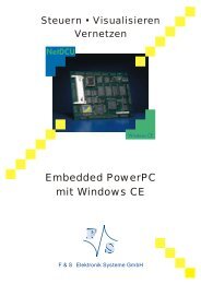
NetDCU-ADP/TX2 - F&S Elektronik Systeme GmbH.
NetDCU-ADP/TX2 - F&S Elektronik Systeme GmbH.
NetDCU-ADP/TX2 - F&S Elektronik Systeme GmbH.

Create successful ePaper yourself
Turn your PDF publications into a flip-book with our unique Google optimized e-Paper software.
<strong>NetDCU</strong>-<strong>ADP</strong>/<strong>TX2</strong><br />
Hardware<br />
Version 1.20 Date 14.03.2011<br />
© by F & S <strong>Elektronik</strong> <strong>Systeme</strong> <strong>GmbH</strong> 2009<br />
F & S <strong>Elektronik</strong> <strong>Systeme</strong> <strong>GmbH</strong><br />
Untere Waldplätze 23<br />
D-70569 Stuttgart<br />
Phone: +49-711-123722-0 Fax: +49-711-123722-99
Table of Contents<br />
1 Overview..................................................................1<br />
2 Arrangement of Connectors ...................................1<br />
3 Connectors..............................................................2<br />
3.1 Counting of the connector pins..................................2<br />
3.2 J1 <strong>NetDCU</strong>................................................................3<br />
3.3 J2 Display .................................................................5<br />
3.4 J3 CFL......................................................................7<br />
3.5 J4 Touch...................................................................7<br />
4 Configuration <strong>NetDCU</strong>-<strong>ADP</strong>/<strong>TX2</strong>.............................8<br />
4.1 Jumpers....................................................................8<br />
4.2 Examples..................................................................9
1 Overview<br />
The <strong>NetDCU</strong>-<strong>ADP</strong>/<strong>TX2</strong> connects the Hitachi TX series<br />
displays with 40 pin connector listed in Chapter 4.2 to the<br />
<strong>NetDCU</strong>.<br />
2 Arrangement of Connectors<br />
Figure 2.1: Top View<br />
J3<br />
1<br />
J1<br />
J2<br />
JP 1 2 3 4 5 6 7 8 910<br />
J4
3 Connectors<br />
3.1 Counting of the connector pins<br />
All double row connectors are counted as follows.<br />
The row with pin 1 contains all odd-numbered pins (1, 3, 5,<br />
etc.), and the opposite row contains all even-numbered pins<br />
(2, 4, 6, etc.).
3.2 J1 <strong>NetDCU</strong><br />
J1 connects to the <strong>NetDCU</strong>. See <strong>NetDCU</strong> documentation for<br />
configuration of the display interface.<br />
J1<br />
Pin Function<br />
1 GND<br />
2 R1<br />
3 R0<br />
4 G5<br />
5 G4<br />
6 G3<br />
7 G2<br />
8 GND<br />
9 B3<br />
10 B2<br />
11 B1<br />
12 B0<br />
13 G1<br />
14 G0<br />
15 B5<br />
16 B4<br />
17 GND<br />
18 NC<br />
19 DCLK
20 NC<br />
21 DTMG<br />
22 NC<br />
23 NC<br />
24 GND<br />
25 VLCD<br />
26 NC<br />
27 NC<br />
28 GND<br />
29 NC<br />
30 VCFL<br />
31 R2<br />
32 R3<br />
33 R4<br />
34 R5
3.3 J2 Display<br />
J2 connects to the display. See display data sheet and chapter<br />
4 for configuration of jumpers JP1-JP10.<br />
J2<br />
Pin Function<br />
1 VLCD<br />
2 VLCD<br />
3 VLCD/GND/NC (*)<br />
4 VLCD/GND/NC (*)<br />
5 NC<br />
6 DTMG<br />
7 GND<br />
8 DCLK/NC (*)<br />
9 GND<br />
10 NC<br />
11 GND<br />
12 B5<br />
13 B4<br />
14 B3<br />
15 GND<br />
16 B2<br />
17 B1<br />
18 B0<br />
19 GND
20 G5<br />
21 G4<br />
22 G3<br />
23 GND<br />
24 G2<br />
25 G1<br />
26 G0<br />
27 GND<br />
28 R5<br />
29 R4<br />
30 R3<br />
31 GND<br />
32 R2<br />
33 R1<br />
34 R0<br />
35 VLCD/NC (*)(**)<br />
36 GND<br />
37 GND/NC (*)(**)<br />
38 DCLK/NC (*)(**)<br />
39 GND/NC (*)(**)<br />
40 GND/NC (*)(**)<br />
(*) see Chapter 4 below<br />
(**) see Chapter 3.5 below
3.4 J3 CFL<br />
J3 is directly connected to the VCFL output of the <strong>NetDCU</strong>.<br />
3.5 J4 Touch<br />
J3<br />
Pin Function<br />
1 VCFL<br />
2 NC<br />
3 GND<br />
J4 can be used to connect the touchpanel of the display to the<br />
<strong>NetDCU</strong>. Connect J4 to the touchpanel pins of the <strong>NetDCU</strong> to<br />
use the touchpanel.<br />
J4<br />
Pin Function<br />
1 Pin 37 of J2<br />
2 Pin 40 of J2<br />
3 Pin 39 of J2<br />
4 Pin 38 of J2<br />
5 Pin 35 of J2<br />
6 GND
4 Configuration <strong>NetDCU</strong>-<strong>ADP</strong>/<strong>TX2</strong><br />
4.1 Jumpers<br />
Jumpers<br />
Jumper Pin J2 Set Not Set<br />
1 3 GND (*) NC<br />
2 3 VLCD (*) NC<br />
3 4 VLCD (*) NC<br />
4 4 GND (*) NC<br />
5 8 DCLK NC<br />
6 35 VLCD NC<br />
7 38 DCLK NC (**)<br />
8 37 GND NC (**)<br />
9 39 GND NC (**)<br />
10 40 GND NC (**)<br />
(*) setting JP1and JP2 or JP3 and JP4 will short VLCD<br />
and GND!<br />
(**) do not set JP7-JP10 when using the touch panel.
4.2 Examples<br />
Examples<br />
Display 1 2 3 4 5 6 7 8 9 10<br />
TX14D11 x x x<br />
TX14D12 x x x<br />
TX14D14 (*) (*) (*) (*) x x<br />
TX16D11 x x x<br />
TX18D16 x x x x x x<br />
TX18D57 x x x x x x<br />
TX18D35 X<br />
<strong>TX2</strong>0D16 x x x x x x<br />
<strong>TX2</strong>0D17 x x x x x x<br />
<strong>TX2</strong>3D12 x x x x x x<br />
TX31D55 x x x x x x<br />
x Jumper set<br />
(*) depends on selected scan direction.
Index<br />
Configuration.........................................................................8<br />
Examples.............................................................................9<br />
Jumpers ..............................................................................8<br />
Connector<br />
Arrangement........................................................................1<br />
CFL .....................................................................................7<br />
Counting..............................................................................2<br />
Display ................................................................................5<br />
<strong>NetDCU</strong>...............................................................................3<br />
Touch ..................................................................................7<br />
Connectors............................................................................2<br />
J1 ..........................................................................................3<br />
J2 ..........................................................................................5<br />
J3 ..........................................................................................7<br />
J4 ..........................................................................................7<br />
Overview ...............................................................................1