Transmutation of metal at low energy in a confined ... - LENR-CANR
Transmutation of metal at low energy in a confined ... - LENR-CANR
Transmutation of metal at low energy in a confined ... - LENR-CANR

You also want an ePaper? Increase the reach of your titles
YUMPU automatically turns print PDFs into web optimized ePapers that Google loves.
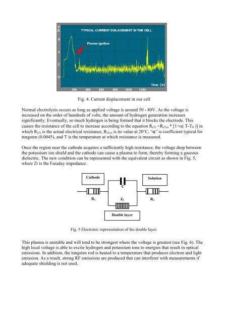
Fig. 4. Current displacement <strong>in</strong> our cell<br />
Normal electrolysis occurs as long as applied voltage is around 50 - 80V. As the voltage is<br />
<strong>in</strong>creased on the order <strong>of</strong> hundreds <strong>of</strong> volts, the amount <strong>of</strong> hydrogen gener<strong>at</strong>ion <strong>in</strong>creases<br />
significantly. Eventually, so much hydrogen is be<strong>in</strong>g formed th<strong>at</strong> it blocks the electrode. This<br />
causes the resistance <strong>of</strong> the cell to <strong>in</strong>crease accord<strong>in</strong>g to the equ<strong>at</strong>ion R(T) =R(To) * [1+T-T0 )] <strong>in</strong><br />
which R(T) is the actual electrical resistance, R(To) is its value <strong>at</strong> 20°C, “”is coefficient typical for<br />
tungsten (0.0045), and T is the temper<strong>at</strong>ure <strong>at</strong> which resistance is measured.<br />
Once the region near the c<strong>at</strong>hode acquires a sufficiently high resistance, the voltage drop between<br />
the potassium ion shield and the c<strong>at</strong>hode can cause a plasma to form, thereby form<strong>in</strong>g a gaseous<br />
dielectric. The new condition can be represented with the equivalent circuit as shown <strong>in</strong> Fig. 5,<br />
where Zf is the Faraday impedance.<br />
C<strong>at</strong>hode Solution<br />
R1<br />
Fig. 5 Electronic represent<strong>at</strong>ion <strong>of</strong> the double layer.<br />
This plasma is unstable and will tend to be strongest where the voltage is gre<strong>at</strong>est (see Fig. 6). The<br />
high local voltage is able to excite hydrogen and potassium ions to energies th<strong>at</strong> result <strong>in</strong> optical<br />
emissions. In addition, the tungsten rod is he<strong>at</strong>ed to a temper<strong>at</strong>ure th<strong>at</strong> produces electron and light<br />
emission. As a result, strong RF emissions are produced th<strong>at</strong> can <strong>in</strong>terferer with measurements if<br />
adequ<strong>at</strong>e shield<strong>in</strong>g is not used.<br />
C<br />
Zf<br />
Double layer<br />
R2