Endoscope Quick Reference Guide - Texas Instruments
Endoscope Quick Reference Guide - Texas Instruments
Endoscope Quick Reference Guide - Texas Instruments

Create successful ePaper yourself
Turn your PDF publications into a flip-book with our unique Google optimized e-Paper software.
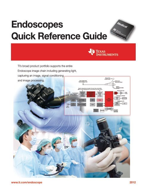
<strong>Endoscope</strong>s<br />
<strong>Quick</strong> <strong>Reference</strong> <strong>Guide</strong><br />
TI’s broad product portfolio supports the entire<br />
<strong>Endoscope</strong> image chain including generating light,<br />
capturing an image, signal conditioning<br />
and image processing.<br />
www.ti.com/endoscope<br />
2012
<strong>Endoscope</strong>s <strong>Quick</strong> <strong>Reference</strong> <strong>Guide</strong><br />
➔<br />
Overview<br />
In medicine, an endoscope is used to look<br />
inside the body to examine organs. Through<br />
a small incision, endoscopes can examine<br />
gastrointestinal, respiratory and urinary<br />
tracts, as well as internal organs. An endoscope<br />
captures images through its long<br />
tube, which can be rigid or flexible.<br />
Additional instruments for cutting, grasping<br />
and other functions are often attached to the<br />
endo scope to permit minimally invasive<br />
procedures that improve patient care and<br />
minimize recovery time.<br />
When used in a technical application to<br />
inspect confined spaces, the tool is often<br />
referred to as a borescope. Bore scopes are<br />
used to inspect machinery interiors, building<br />
walls and to search for victims in collapsed<br />
buildings.<br />
<strong>Endoscope</strong>s and borescopes have four<br />
basic requirements:<br />
• A light source to illuminate the subject<br />
• A tube to guide the light to the subject<br />
• A lens or fiber optic system to capture<br />
light reflected from the subject<br />
• An image-capture system to capture,<br />
process and store or display the image<br />
TI’s broad product portfolio supports the<br />
entire image chain including generating light,<br />
capturing an image, signal conditioning and<br />
image processing. LED drivers supply a<br />
Lens<br />
Light<br />
Source<br />
LEGEND<br />
Processor<br />
Interface<br />
Amplifier<br />
Logic<br />
Power<br />
ADC/DAC<br />
Other<br />
CCD/CMOS<br />
Sensor<br />
Imager<br />
Power<br />
LED<br />
Drivers<br />
<strong>Endoscope</strong> system block diagram.<br />
Lens, Imager and<br />
Optional Biopsy Tool<br />
Optional<br />
Analog<br />
Line<br />
Drivers<br />
Low Noise<br />
Power Rails<br />
System Power<br />
Overview ......................................................2<br />
<strong>Endoscope</strong> Solutions ..........................................3<br />
Selection Tables ...............................................x<br />
Resources .....................................................x<br />
bright light source with excellent directionality<br />
and minimal waste heat. These drivers are<br />
versatile and permit LED selection optimized<br />
for an application’s spectral requirements.<br />
The resolution of current steps impacts<br />
illumination control precision: PWM and<br />
analog dimming available from TI LED drivers<br />
allow for precise illumination level and<br />
timing control.<br />
The image sensor detects reflected light and<br />
converts the light to an analog electrical<br />
signal. Depending on the image sensor’s<br />
location, low-noise line drivers may be<br />
needed to transmit the signal over the light<br />
tube’s length. Critical considerations for line<br />
drivers are low power, noise immunity and<br />
data rate. LVDS technology provides up to<br />
800 Mbps with voltage swings of a few<br />
tenths of a volt and high rejection of common-mode<br />
noise.<br />
Essential to final image quality is the analog<br />
front end (AFE). The AFE conditions the<br />
Need is dependent on length of scope tube and whether<br />
AFE is in the imagining end or processing end of the scope.<br />
CCD/CMOS<br />
Signal<br />
Processing<br />
(AFE)<br />
REF<br />
Logic<br />
Memory<br />
Power<br />
2<br />
Optional<br />
Digital<br />
Line<br />
Drivers<br />
Clock<br />
Core and<br />
I/O Power<br />
SDRAM<br />
Biopsy Tool<br />
Control Head<br />
Video<br />
Processing<br />
Engine<br />
Level Shift<br />
sensor’s analog electrical signal and converts<br />
image information to a digitized representation.<br />
Critical to AFE selection is the ability to<br />
condition the signal to correct sensor-induced<br />
distortions such as dark current cancellation,<br />
reset level variations, defective pixel correction<br />
and DC offset variations. Depending on<br />
the signal level, the presence of programmable<br />
gain amplifiers (PGAs), PGA linearity<br />
and the range of available gains may also be<br />
important. During digitization, the number of<br />
bits determines image contrast. Typically,<br />
digitizing the initial data with two to four bits<br />
more precision than desired in the final image<br />
is recommended. For example, if 8 bits of final<br />
image data are required, initially digitize to 10<br />
bits to allow for rounding errors during image<br />
processing. When color reproduction is critical,<br />
differential non-linearity (DNL) and integral<br />
non-linearity (INL) should be minimized.<br />
For more information, visit<br />
www.ti.com/endoscope<br />
<strong>Endoscope</strong><br />
Electronics Head<br />
DAC<br />
System<br />
Connection Cable<br />
Analog Video Out<br />
Interfaces to Display<br />
HDMI<br />
DVI<br />
Interfaces to PC<br />
RS232<br />
RS485<br />
Ethernet<br />
FLASH<br />
EPROM<br />
Product Availability and Design Disclaimer – The system block diagram depicted above and the devices recommended are designed in this manner as a reference. Please contact your local TI sales office or<br />
distributor for system design specifics and product availability.<br />
RGB<br />
Video
<strong>Endoscope</strong>s <strong>Quick</strong> <strong>Reference</strong> <strong>Guide</strong><br />
➔<br />
<strong>Endoscope</strong> Solutions<br />
Digital Media System-on-Chip<br />
TMS320DM368<br />
For more information, visit: www.ti.com/sc/device/TMS320DM368<br />
Key Features<br />
• HD video processing at 1080p<br />
30 fps H.264<br />
• 432-MHz ARM926EJ-S clock rate<br />
• Two video image co-processor<br />
(HDVICP, MJCP) engines<br />
• 3.3-V and 1.8-V I/O, 1.35-V core<br />
• Extended temperatures available<br />
Applications<br />
• DLP ® spectroscopy<br />
• <strong>Endoscope</strong><br />
Developers can now deliver crystal clear multi-format video at up to 1080p H.264<br />
at 30 fps (encode and closed-looped decode) in their designs without concerns of<br />
video format support, constrained network bandwidth, limited system storage<br />
capacity or cost with the new TMS320DM368 DaVinci video processor from<br />
<strong>Texas</strong> <strong>Instruments</strong>.<br />
The DM368 is capable of achieving HD video processing at 1080p 30fps H.264<br />
and is completely pin-to-pin compatible with the DM365 processors, using the<br />
same ARM926EJ-S core running at 432 MHz. This ARM9-based DM368 device<br />
supports production-qualified H.264BP/MP/HP, MPEG-4, MPEG-2, MJPEG and<br />
VC1/WMV9 codecs, providing customers with the flexibility to select the right<br />
video codec for their application.<br />
Camera<br />
AFE<br />
SDTV/HDTV<br />
Analog Video<br />
Digital<br />
RGB/YUV<br />
VPSS<br />
Face Det Lens Dist<br />
Video FE<br />
3Ch<br />
DAC<br />
JTAG<br />
I/F<br />
ISIF<br />
3<br />
Video BE<br />
HDVICP MJCP<br />
TMS320DM368 system block diagram.<br />
IPIPE<br />
Resizer<br />
Video<br />
Encoder OSD<br />
CLOCK Ctrl<br />
PLL<br />
r<br />
e<br />
f<br />
f<br />
u<br />
B<br />
ARM926EJ-S<br />
I-Cache<br />
16 KB<br />
D-Cache<br />
8 KB<br />
19.2 MHz, 24 MHz 32.768<br />
27 MHz or 36 MHz kHz<br />
ARM INTC<br />
PRTCSS<br />
RAM<br />
32 KB<br />
ROM<br />
16 KB<br />
EDMA<br />
DDR2<br />
Controller<br />
DMA/Data and Configuration Bus<br />
PMIC/<br />
SW<br />
NAND/SM<br />
Memory<br />
I/F<br />
HPI<br />
USB2.0 HS w/OTG<br />
MMC/SD (x2)<br />
SPI (x5)<br />
UART (x2)<br />
I2C<br />
Timer (x4-64b)<br />
WDT (x1-64b)<br />
GIO<br />
PWM (x4)<br />
RTO<br />
McBSP<br />
EMAC<br />
ADC<br />
Key Scan<br />
Voice Codec<br />
16 Bit<br />
8/16 Bit<br />
16 Bit<br />
16-Bit<br />
DDR2/<br />
mDDR<br />
NAND/<br />
OneNAND/<br />
NOR Flash,<br />
SmartMedia/<br />
xD<br />
Host CPU<br />
System<br />
I/O<br />
Interface
<strong>Endoscope</strong>s <strong>Quick</strong> <strong>Reference</strong> <strong>Guide</strong><br />
➔ <strong>Endoscope</strong> Solutions<br />
16-Bit Ultra-Low-Power MCU<br />
MSP430F4481<br />
For more information, visit: www.ti.com/sc/device/MSP430F4481<br />
Key Features<br />
• Low supply-voltage range,<br />
1.8 V to 3.6 V<br />
• Ultra-low-power consumption<br />
• 2-bit A/D converter with internal<br />
reference<br />
• 16-bit RISC architecture<br />
• Supply voltage supervisor/monitor<br />
with programmable level detection<br />
Applications<br />
• <strong>Endoscope</strong><br />
The device architecture, combined with five low-power modes, is optimized to<br />
achieve extended battery life in portable measurement applications. The device<br />
features a powerful 16-bit RISC CPU, 16-bit registers, and constant generators<br />
that contribute to maximum code efficiency. The digitally controlled oscillator<br />
(DCO) allows wake-up from low-power modes to active mode in less than 6 µs.<br />
The MSP430F4481 has a configuration with two built-in 16-bit timers, one or two<br />
universal serial synchronous/asynchronous communication interfaces (USART), 48<br />
I/O pins, and a liquid crystal driver (LCD) with up to 160 segments.<br />
XT2IN<br />
XT2OUT<br />
XIN<br />
XOUT<br />
Oscillator<br />
FLL+<br />
MCLK<br />
8 MHz<br />
CPU<br />
incl. 16<br />
Registers<br />
Emulation<br />
Module<br />
JTAG<br />
Interface<br />
ACLK<br />
SMCLK<br />
4<br />
DVCC1/2 DVSS1/2 AVCC AVSS<br />
P1<br />
8<br />
MAB<br />
MDB<br />
MSP430F4481 system block diagram.<br />
Flash<br />
60KB<br />
48KB<br />
Hardware<br />
Multiplier<br />
MPY, MPYS<br />
MAC,MACS<br />
RAM<br />
2KB<br />
POR/<br />
SVS/<br />
Brownout<br />
RST/NMI<br />
Port 1<br />
8 I/O<br />
Interrupt<br />
Capability<br />
P2<br />
8<br />
Port 2<br />
8 I/O<br />
Interrupt<br />
Capability<br />
Watchdog<br />
Timer<br />
WDT<br />
15/16-Bit<br />
P3<br />
8<br />
Port 3<br />
8 I/O<br />
Timer_B7<br />
7 CC Reg<br />
Shadow<br />
Reg<br />
P4<br />
8<br />
Port 4<br />
8 I/O<br />
Timer_A3<br />
3 CC Reg<br />
P5<br />
8<br />
Port 5<br />
8 I/O<br />
Comparator_<br />
A<br />
P6<br />
8<br />
Port 6<br />
6 I/O<br />
Basic<br />
Timer 1<br />
1 Interrupt<br />
Vector<br />
f LCD<br />
USART0<br />
USART1<br />
UART Mode<br />
SPI Mode<br />
LCD<br />
160<br />
Segments<br />
1,2,3,4 MUX
<strong>Endoscope</strong>s <strong>Quick</strong> <strong>Reference</strong> <strong>Guide</strong><br />
➔<br />
<strong>Endoscope</strong> Solutions<br />
5-Channel Power Mgmt IC<br />
TPS65053<br />
For more information, visit: www.ti.com/sc/device/TPS65053<br />
Key Features<br />
• Up to 95% efficiency<br />
• 2.5 V to 6 V V IN range for DC/DC<br />
converters<br />
• 2.25-MHz fixed frequency operation<br />
• Output current of up to 1 A on the<br />
DCDC1 converter<br />
• 180° out-of-phase operation<br />
• Output voltage accuracy in PWM<br />
mode ±1%<br />
• Total typical 32-µA quiescent current<br />
for both DC/DC converters<br />
• 100% duty cycle for lowest dropout<br />
Applications<br />
• Oscilloscope<br />
• Pulse oximetry<br />
The TPS65053 is an integrated Power Management IC for applications powered<br />
by one Li-Ion or Li-Polymer cell, which require multiple power rails. The device<br />
provides two highly efficient, 2.25 MHz step-down converters targeted at providing<br />
the core voltage and I/O voltage in a processor based system. Both step-down<br />
converters enter a low power mode at light load for maximum efficiency across<br />
the widest possible range of load currents. For low noise applications the devices<br />
can be forced into fixed frequency PWM mode by pulling the MODE pin high.<br />
Both converters allow the use of small inductors and capacitors to achieve a small<br />
solution size. TPS65053 provides an output current of up to 1 A on the DCDC1<br />
converter and up to 0.<br />
VIN<br />
ENABLE<br />
MODE<br />
ENABLE<br />
VIN<br />
2.2 F<br />
ENABLE<br />
ENABLE<br />
1<br />
1 F<br />
VIN<br />
2.2 F<br />
ENABLE<br />
THRESHOLD<br />
VCC<br />
EN_DCDC1<br />
EN_DCDC2<br />
VIN_LDO1<br />
EN_LDO1<br />
VIN_LDO2/3<br />
EN_LDO2<br />
EN_LDO3<br />
TPS65053 system block diagram.<br />
5<br />
RESET<br />
AGND<br />
STEP-DOWN<br />
CONVERTER<br />
STEP-DOWN<br />
CONVERTER<br />
600mA<br />
VLDO1<br />
VLDO2<br />
VLDO3<br />
VINDCDC1/2<br />
L1<br />
FB_DCDC1<br />
PGND1<br />
L2<br />
FB_DCDC2<br />
PGND2<br />
VLDO1<br />
FB1<br />
VLDO2<br />
FB2<br />
VLDO3<br />
Reset<br />
2.2 H<br />
2.2 H<br />
R5<br />
R6<br />
R7<br />
R8<br />
R1<br />
R2<br />
R3<br />
R4<br />
22 F<br />
Cff<br />
Cff<br />
4.7 F<br />
2.2 F<br />
2.2 F<br />
10 F<br />
10 F<br />
R19
<strong>Endoscope</strong>s <strong>Quick</strong> <strong>Reference</strong> <strong>Guide</strong><br />
➔<br />
<strong>Endoscope</strong> Solutions<br />
1 A SIMPLE SWITCHER ® Nano Module<br />
LMZ10501<br />
For more information, visit: www.ti.com/sc/device/LMZ10501<br />
Key Features<br />
• Easy-to-use step-down DC-DC<br />
solution<br />
• Drive up to 1 A load<br />
• Point-of-load conversions from<br />
3.3 V and 5 V rails<br />
Applications<br />
• <strong>Endoscope</strong><br />
• Low output noise applications<br />
• Space constrained applications<br />
The LMZ10501 SIMPLE SWITCHER ® nano module is an easy-to-use step-down<br />
DC-DC solution capable of driving up to 1 A load in space-constrained applications.<br />
Only an input capacitor, an output capacitor, a small V CON filter capacitor, and<br />
two resistors are required for basic operation. The nano module comes in 8-pin<br />
LLP footprint package with an integrated inductor. Internal current limit based<br />
soft-start function, current overload protection, and thermal shutdown are also<br />
provided.<br />
V CON<br />
FB<br />
EN<br />
V IN<br />
UVLO<br />
LMZ10501 system block diagram.<br />
6<br />
Error<br />
Amplifier<br />
COMP<br />
Main Control<br />
Oscillator<br />
V REF<br />
<strong>Reference</strong><br />
Voltage<br />
Current<br />
Comp<br />
MOSFET<br />
Control<br />
Logic<br />
TSD<br />
SGND<br />
Current<br />
Sense<br />
V IN<br />
PGND<br />
UVLO<br />
L<br />
Integrated<br />
Inductor<br />
V OUT
<strong>Endoscope</strong>s <strong>Quick</strong> <strong>Reference</strong> <strong>Guide</strong><br />
➔<br />
<strong>Endoscope</strong> Solutions<br />
525 kHz/1.6 MHz Constant Current Boost and SEPIC LED Driver<br />
LM3410<br />
For more information, visit: www.ti.com/sc/device/LM3410<br />
Key Features<br />
• Input voltage range of 2.7 V to 5.5 V<br />
• Output voltage range of 3 V to 24 V<br />
• 2.8 A typical switch current<br />
• High switching frequency<br />
• Thermal shutdown<br />
• 190 mV internal voltage reference<br />
Applications<br />
• <strong>Endoscope</strong><br />
The LM3410 constant current LED driver is a monolithic, high frequency, PWM<br />
DC/DC converter in 5-pin SOT23, 6-pin LLP, & 8-pin eMSOP packages. With a<br />
minimum of external components the LM3410 is easy to use. It can drive 2.8A<br />
typical peak currents with an internal 170 mΩ NMOS switch. Switching frequency<br />
is internally set to either 525 kHz or 1.60 MHz, allowing the use of extremely<br />
small surface mount inductors and chip capacitors. Even though the operating<br />
frequency is high, efficiencies up to 88% are easy to achieve. External shutdown<br />
is included, featuring an ultra-low standby current of 80 nA. The LM3410 utilizes<br />
current-mode control and internal compensation to provide high-performance over<br />
a wide range of operating conditions. Additional features include dimming, cycleby-cycle<br />
current limit, and thermal shutdown.<br />
VIN<br />
C 1<br />
DIMM 4<br />
DIM<br />
7<br />
5<br />
VIN<br />
LM3410 typical boost application circuit.<br />
L 1<br />
3<br />
FB<br />
2<br />
GND<br />
1<br />
SW<br />
D 1<br />
R 1<br />
C 2
<strong>Endoscope</strong>s <strong>Quick</strong> <strong>Reference</strong> <strong>Guide</strong><br />
➔<br />
<strong>Endoscope</strong> Solutions<br />
Three 10-Bit Video DAC<br />
THS8135<br />
For more information, visit: www.ti.com/sc/device/THS8135<br />
Key Features<br />
• Operates from 3.3-V analog and<br />
1.8-V digital supplies<br />
• 240-MSPS operation<br />
• Three 10-bit D/A converters<br />
• YPbPr/RGB configurable blanking<br />
levels<br />
• Integrated sync-on-green/luminance or<br />
sync-on-all composite sync insertion<br />
• Internal voltage reference<br />
• Low-power operation From 3.3-V<br />
analog and 1.8-V digital supply levels<br />
Applications<br />
• <strong>Endoscope</strong><br />
The THS8135 is a general-purpose triple high-speed D/A converter optimized for<br />
use in video/graphics applications. The device operates from 3.3-V analog and<br />
1.8-V digital supplies. The THS8135 performance is assured at a sampling rate up<br />
to 240 MSPS. The THS8135 consists of three 10-bit D/A converters and additional<br />
circuitry for bi-level/tri-level sync and blanking level generation. By providing a DC<br />
offset for the lowest video amplitude output in video DAC mode, the device can<br />
insert a (negative) bi-level or (negative/positive) tri-level sync on either only the<br />
green/luminance (sync-on-green/sync-on-Y) channel or on all channels for video<br />
applications. A generic DAC mode avoids this dc offset, making this device suitable<br />
for non-video applications as well.<br />
RCr[9:0]<br />
R/Cr<br />
DAC<br />
Register<br />
GY[9:0]<br />
BCb[9:0]<br />
THS8135 system block diagram.<br />
3G/HD/SD Video Clock Generator with Audio Clock<br />
LMH1983<br />
For more information, visit: www.ti.com/sc/device/LMH1983<br />
Key Features<br />
• Four PLLs for simultaneous A/V<br />
clock generation<br />
• 3.3 V single supply operation<br />
• Flexible PLL bandwidth to optimize<br />
jitter performance and lock time<br />
• 3 x 2 Video clock crosspoint<br />
Applications<br />
• <strong>Endoscope</strong><br />
525i<br />
Analog<br />
ref. in<br />
LMH1981<br />
Sync<br />
Separator<br />
8<br />
CLK<br />
M1<br />
M2<br />
H sync<br />
V sync<br />
F sync<br />
DVDD DVSS COMP FSADJ VREF<br />
Input<br />
Formatter<br />
Configuration<br />
Control<br />
Bandgap<br />
<strong>Reference</strong><br />
G/Y<br />
Register<br />
B/Cb<br />
Register<br />
DAC<br />
DAC<br />
SYNC/BLANK<br />
Control<br />
AVDD AVSS SYNC BLANK<br />
SYNC_T<br />
The LMH1983 is a highly-integrated programmable audio/video (A/V) clock generator.<br />
It can replace multiple PLLs and VCXOs used in applications supporting<br />
SMPTE serial digital video (SDI) and digital audio AES3/EBU standards. It offers<br />
low-jitter reference clocks for any SDI transmitter to meet stringent output jitter<br />
specifications without additional clock cleaning circuits.<br />
LMH1983 typical application.<br />
H IN<br />
V IN<br />
F IN<br />
Loop<br />
Filter<br />
LMH1983<br />
27 MHz<br />
VCXO<br />
27 MHz (PLL1)<br />
CLKout1<br />
29.97 Hz (TOF1)<br />
148.5 MHz (PLL2)<br />
CLKout2<br />
29.97 Hz (TOF2)<br />
148.35 MHz (PLL3)<br />
CLKout3<br />
59.94 Hz (TOF3)<br />
24.576 MHz (PLL4)<br />
CLKout4<br />
5.994 Hz<br />
Genlocked to video ref. in<br />
FPGA<br />
A/V Frame Sync with<br />
Downconverter,<br />
Audio Embedder and<br />
De-embedder<br />
ARPr<br />
AGY<br />
ABPb<br />
525i/29.97 SDI out<br />
+ embedded audio<br />
1080p/59.94 SDI out<br />
+ embedded audio<br />
1080p/59.94 SDI in<br />
+ embedded audio
<strong>Endoscope</strong>s <strong>Quick</strong> <strong>Reference</strong> <strong>Guide</strong><br />
➔<br />
Selection Table<br />
Component Recommendations<br />
Component Description Key Features Benefits Other TI Solutions<br />
Analog Front Ends<br />
VSP2582 CCD/CMOS AFE 36MSPS, 12-bits (parallel output), CDS Low noise, low power, smallest footprint<br />
VSP2562 CCD/CMOS Analog<br />
Front End<br />
VSP2566 CCD/CMOS Analog<br />
Front End<br />
Processors<br />
OMAP3530 Applications<br />
Processor<br />
TMS320DM355 Digital Media<br />
System-on-Chip<br />
TMS320DM365 Digital Media<br />
System-on-Chip<br />
TMS320DM368<br />
*Page 3<br />
Digital Media<br />
System-on-Chip<br />
TMS320DM6437 Digital Media<br />
Processor<br />
TMS320DM6446 Digital Media<br />
System-on-Chip<br />
TMS320DM6467 Digital Media<br />
System-on-Chip<br />
TMS320C6747 Industry’s Lowest<br />
Power Floating-<br />
Point DSP<br />
Microcontrollers<br />
MSP430F4481 16-Bit Ultra-Low-<br />
*Page 4 Power MCU<br />
Data Converters<br />
THS8135<br />
*Page 8<br />
36MSPS, 12-bits (parallel output), CDS, w/two<br />
8-bit DACs<br />
36MSPS, 16-bits (parallel output), CDS, w/two<br />
8-bit DACs<br />
ARM ® Cortex-A8, C64x+, graphics accelerator, video<br />
accelerators<br />
64-channel EDMA, 135/216/270MHz ARM926EJ-S<br />
clock rate<br />
64-channel EDMA, 216/270/300MHz ARM926EJ-S<br />
clock rate<br />
HD video processing at 1080p, 432-MHz ARM926EJ-S<br />
clock rate<br />
64-channel EDMA, 400/500/600/660/700MHz<br />
C64x+ clock rate<br />
9<br />
Low noise, low power, small footprint, includes two<br />
8-bit DACs to simplify system design<br />
Higher resolution, low noise, low power, small footprint,<br />
includes two 8-bit DACs to simplify system design<br />
Laptop-like performance at handheld power levels OMAP3503,<br />
OMAP3515, OMAP3525<br />
Encode/decode up to 720p H.264; optimized for<br />
power, cost, and efficiency, and is even suitable for<br />
three Li-ion AA battery inputs<br />
Encode/decode up to 1080p H.264; high-performance<br />
ARM ® and video processing capabilities<br />
Deliver crystal clear multi-format video at up to 1080p<br />
H.264 at 30 fps<br />
DSP architecture means programmable solution,<br />
Benefit from H.264 encode (D1)<br />
64-channel EDMA, 513/594MHz C64x+ clock rate Encode/decode up to 720p MPEG-4, programmable<br />
DSP, with GUI and other processing offloaded to the<br />
ARM ® for greater efficiency and scalability<br />
64-channel EDMA, 594/729/1000MHz C64x+ clock<br />
rate<br />
32-/64-bit accuracy, 1.8V to 3.3V I/O supply, low power<br />
and rich connectivity peripherals.<br />
1.8 V to 3.6 V supply voltage, ultra-low-power<br />
consumption, 16-bit RISC architecture<br />
Video DAC Triple 10-bit 240MSPS video DAC with tri-level sync<br />
and video-compliant (ITU-R.BT601) full-scale range<br />
Encode/decode up to 1080p H.264; high-performance<br />
programmable DSP and ARM<br />
Uses three times less power that existing floatingpoint<br />
DSPs<br />
Optimized to achieve extended battery life in portable<br />
measurement applications<br />
THS8200<br />
Amplifiers<br />
Video DAC Triple 10-bit all-format video DAC<br />
LMH6683 Video Amp 190MHz single supply triple op amps Provides excellent differential gain and phase<br />
combined with output current drive, making it ideal for<br />
video processing<br />
LMH6733 Video Amp Single-Supply 1GHz low power triple op amps Offers single/split supply operation, wide gain range, and<br />
stability without external compensation at unity gain<br />
LMH6738 Video Amp Wideband low distortion triple op amps Offers single/split supply operation, wide gain range, and<br />
stability without external compensation at unity gain<br />
OPA360 Video Amp 3V video amplifier with low pass filter, internal G=2 and<br />
SAG correction in SC70<br />
Designed to work with video processors OPA361, THS7303<br />
OPA3693<br />
OPA830<br />
Video Amp<br />
Buffer Amp<br />
Triple,ultra-wideband, fixed gain, video buffer w/disable<br />
250MHz (G = +1) BW, 550V/µs slew rate, 9.2nV/√<br />
Designed to work with video processors OPA3832<br />
— Hz<br />
noise, 3.9mA supply current, single/dual supply<br />
Ideal input buffer stage OPA2830, OPA847<br />
Interface/Video/Clock<br />
LMH1983<br />
*Page 8<br />
3G/HD/SD Video<br />
Clock Generator<br />
with Audio Clock<br />
LMK03806 High Performance,<br />
Ultra Low Jitter<br />
Clock Generator with<br />
14 Programmable<br />
Outputs<br />
LMK04100 Precision Clock<br />
Jitter Cleaner<br />
with Cascaded<br />
PLLs<br />
3.3 V single supply operation, 3 x 2 video clock<br />
crosspoint<br />
High performance clock generator delivers ultra low<br />
RMS jitter < 150 fs and generates multiple clocks from<br />
low cost crystal/external clock<br />
High performance clock jitter cleaner provides jitter<br />
cleaning, clock multiplication, and distribution without<br />
the need for high-performance VCXO modules &<br />
generates 5 ultra low jitter clocks in LVCMOS, LVDS, or<br />
LVCPECL formats<br />
LMH6738 Buffer Amp 2.5MHz (G = +1) BW, 550V/µs slew rate, 9.2nV/√ — Hz<br />
noise, 3.9mA supply current, single/dual supply<br />
SN65LVDS93A 24-bit RGB LVDS<br />
Serdes<br />
10MHz-135MHz, BGA and TSSOP; supports 1.8V to<br />
3.3V TTL i/p<br />
It offers low-jitter reference clocks for any<br />
SDI transmitter to meet stringent output jitter<br />
specifications without additional clock cleaning<br />
circuits.<br />
Reduces board area and BOM cost by 50% against<br />
competing approach<br />
Delivers high performance and significantly reduces<br />
BOM cost<br />
Ideal input buffer stage OPA2830, OPA847<br />
Wide frequency range, saves space, no level shifter for<br />
1.8V powered µP<br />
*For additional product information see designated page number. To view more system block diagram compatible products, visit www.ti.com/endoscope<br />
SN75LVDS83B
Component Recommendations (continued)<br />
Component Description Key Features Benefits Other TI Solutions<br />
Power Management<br />
LMZ10501<br />
*Page 6<br />
LM3410<br />
*Page 7<br />
1 A SIMPLE<br />
SWITCHER ® Nano<br />
Module<br />
525 kHz/1.6 MHz<br />
Constant Current<br />
Boost and SEPIC<br />
LED Driver<br />
Easy-to-use step-down DC-DC solution, drive up to 1 A<br />
load, point-of-load conversions from 3.3 V and 5 V rails<br />
Input voltage range of 2.7 V to 5.5 V; output voltage<br />
range of 3 V to 24 V; 2.8 A typical switch current<br />
This device is an easy-to-use step-down DC-DC<br />
solution capable of driving up to 1 A load in spaceconstrained<br />
applications.<br />
Additional features include dimming, cycle-by-cycle<br />
current limit, and thermal shutdown.<br />
TPS65073 PMU w/charger/<br />
WLED<br />
Integrates charger, WLED, DCDC and LDO. Highest integration for portable applications TPS65720<br />
TPS61160 White LED Driver White LED driver with digital and PWM brightness<br />
control in 2mm x 2mm package<br />
Allows stepped brightness adjustment TPS61061<br />
TPS61220 Boost Converter Down to 0.7V VIN operation, pass-through function Simple, small, low power solution TPS61070<br />
TPS62230 Step-Down Up to 90dB PSRR, excellent AC and transient load Low noise regulation, 12mm<br />
Converter regulation<br />
2 solution size TPS62260<br />
TPS62400 Dual Output Step- 180 degrees out of phase operation, serial interface Flexible voltage adjustment for processors and MCUs TPS62410, TPS62111,<br />
Down Converter<br />
TPS62260, TPS62290<br />
TPS63030 Buck-Boost 1A switch, automatic transition between step down and Extending application run time, small solution TPS61020<br />
Converter boost mode<br />
TPS65053 5-Channel Power Up to 95% efficiency; 2.5 V to 6 V VIN range for DC/DC The device provides two highly efficient, 2.25 MHz TPS62410, TPS62111,<br />
*Page 5 Mgmt IC<br />
converters; 2.25-MHz fixed frequency operation step-down converters that both allow the use of small<br />
inductors and capacitors to achieve a small solution size.<br />
TPS62260, TPS62290<br />
TPS71701 LDO Low-noise, high-bandwidth-PSRR, low-dropout 150mA Filters out wider range of incoming noise with the high TPS718xx family<br />
linear regulator<br />
PSRR<br />
TPS74201 Single Channel<br />
LDO<br />
1.5A ultra low-dropout linear regulator Split bias and supply pin minimize heat generation TPS4401<br />
TPS74301 LDO Single-output LDO, 1.5A, adjustable (0.8V to 3.3V), any Adjust the voltage ramp rate for your processor<br />
or no cap, programmable soft start<br />
requirements<br />
TPS74401 LDO Single-output LDO, 3.0A, adjustable (0.8V to 3.3V), fast Adjust the voltage ramp rate for your processor<br />
transient response, programmable soft start<br />
requirements<br />
TPS74701 Single Channel LDO 1.5A ultra low-dropout linear regulator Split bias and supply pin minimize heat generation TPS71718, TPS74801<br />
TPS75003 Linear Charge Integrated triple-supply power management IC for Provides all three rails in one package<br />
Management Xilinx Spartan FPGAs<br />
*For additional product information see designated page number. To view more system block diagram compatible products, visit www.ti.com/endoscope<br />
TI Worldwide Technical Support<br />
Internet<br />
TI Semiconductor Product Information Center<br />
Home Page<br />
support.ti.com<br />
TI E2E Community Home Page<br />
e2e.ti.com<br />
Product Information Centers<br />
Americas Phone +1(972) 644-5580<br />
Brazil Phone 0800-891-2616<br />
Mexico Phone 0800-670-7544<br />
Fax +1(972)927-6377<br />
Internet support.ti.com/sc/pic/americas.htm<br />
Europe, Middle East, and Africa<br />
Phone<br />
European Free Call 00800-ASK-TEXAS<br />
(00800 275 83927)<br />
International +49 (0) 8161 80 2121<br />
Russian Support +7 (4) 95 98 10 701<br />
Note: The European Free Call (Toll Free) number<br />
is not active in all countries. If you have technical<br />
difficulty calling the free call number, please use the<br />
international number above.<br />
Fax +49 (0) 8161 80 2045<br />
Internet www.ti.com/asktexas<br />
Direct Email asktexas@ti.com<br />
Japan<br />
Phone Domestic 0120-92-3326<br />
Fax International +81-3-3344-5317<br />
Domestic 0120-81-0036<br />
Internet<br />
International support.ti.com/sc/pic/japan.htm<br />
Domestic www.tij.co.jp/pic<br />
Asia<br />
Phone<br />
International +91-80-41381665<br />
Domestic Toll-Free Number<br />
Note: Toll-free numbers do not support<br />
mobile and IP phones.<br />
Australia 1-800-999-084<br />
China 800-820-8682<br />
Hong Kong 800-96-5941<br />
India 1-800-425-7888<br />
Indonesia 001-803-8861-1006<br />
Korea 080-551-2804<br />
Malaysia 1-800-80-3973<br />
New Zealand 0800-446-934<br />
Philippines 1-800-765-7404<br />
Singapore 800-886-1028<br />
Taiwan 0800-006800<br />
Thailand 001-800-886-0010<br />
Fax +8621-23073686<br />
Email tiasia@ti.com or ti-china@ti.com<br />
Internet support.ti.com/sc/pic/asia.htm<br />
D011012<br />
Important Notice: The products and services of <strong>Texas</strong><br />
<strong>Instruments</strong> Incorporated and its subsidiaries described herein are<br />
sold subject to TI’s standard terms and conditions of sale.<br />
Customers are advised to obtain the most current and complete<br />
information about TI products and services before placing orders. TI<br />
assumes no liability for applications assistance, customer’s<br />
applications or product designs, software performance, or<br />
infringement of patents. The publication of information regarding<br />
any other company’s products or services does not constitute TI’s<br />
approval, warranty or endorsement thereof.<br />
The platform bar and E2E are trademarks of <strong>Texas</strong> <strong>Instruments</strong>. All<br />
other trademarks are the property of their respective owners.<br />
© 2012 <strong>Texas</strong> <strong>Instruments</strong> Incorporated<br />
Printed in U.S.A. by (Printer, City, State)<br />
SLYY030
IMPORTANT NOTICE<br />
<strong>Texas</strong> <strong>Instruments</strong> Incorporated and its subsidiaries (TI) reserve the right to make corrections, modifications, enhancements, improvements,<br />
and other changes to its products and services at any time and to discontinue any product or service without notice. Customers should<br />
obtain the latest relevant information before placing orders and should verify that such information is current and complete. All products are<br />
sold subject to TI’s terms and conditions of sale supplied at the time of order acknowledgment.<br />
TI warrants performance of its hardware products to the specifications applicable at the time of sale in accordance with TI’s standard<br />
warranty. Testing and other quality control techniques are used to the extent TI deems necessary to support this warranty. Except where<br />
mandated by government requirements, testing of all parameters of each product is not necessarily performed.<br />
TI assumes no liability for applications assistance or customer product design. Customers are responsible for their products and<br />
applications using TI components. To minimize the risks associated with customer products and applications, customers should provide<br />
adequate design and operating safeguards.<br />
TI does not warrant or represent that any license, either express or implied, is granted under any TI patent right, copyright, mask work right,<br />
or other TI intellectual property right relating to any combination, machine, or process in which TI products or services are used. Information<br />
published by TI regarding third-party products or services does not constitute a license from TI to use such products or services or a<br />
warranty or endorsement thereof. Use of such information may require a license from a third party under the patents or other intellectual<br />
property of the third party, or a license from TI under the patents or other intellectual property of TI.<br />
Reproduction of TI information in TI data books or data sheets is permissible only if reproduction is without alteration and is accompanied<br />
by all associated warranties, conditions, limitations, and notices. Reproduction of this information with alteration is an unfair and deceptive<br />
business practice. TI is not responsible or liable for such altered documentation. Information of third parties may be subject to additional<br />
restrictions.<br />
Resale of TI products or services with statements different from or beyond the parameters stated by TI for that product or service voids all<br />
express and any implied warranties for the associated TI product or service and is an unfair and deceptive business practice. TI is not<br />
responsible or liable for any such statements.<br />
TI products are not authorized for use in safety-critical applications (such as life support) where a failure of the TI product would reasonably<br />
be expected to cause severe personal injury or death, unless officers of the parties have executed an agreement specifically governing<br />
such use. Buyers represent that they have all necessary expertise in the safety and regulatory ramifications of their applications, and<br />
acknowledge and agree that they are solely responsible for all legal, regulatory and safety-related requirements concerning their products<br />
and any use of TI products in such safety-critical applications, notwithstanding any applications-related information or support that may be<br />
provided by TI. Further, Buyers must fully indemnify TI and its representatives against any damages arising out of the use of TI products in<br />
such safety-critical applications.<br />
TI products are neither designed nor intended for use in military/aerospace applications or environments unless the TI products are<br />
specifically designated by TI as military-grade or "enhanced plastic." Only products designated by TI as military-grade meet military<br />
specifications. Buyers acknowledge and agree that any such use of TI products which TI has not designated as military-grade is solely at<br />
the Buyer's risk, and that they are solely responsible for compliance with all legal and regulatory requirements in connection with such use.<br />
TI products are neither designed nor intended for use in automotive applications or environments unless the specific TI products are<br />
designated by TI as compliant with ISO/TS 16949 requirements. Buyers acknowledge and agree that, if they use any non-designated<br />
products in automotive applications, TI will not be responsible for any failure to meet such requirements.<br />
Following are URLs where you can obtain information on other <strong>Texas</strong> <strong>Instruments</strong> products and application solutions:<br />
Products Applications<br />
Audio www.ti.com/audio Automotive and Transportation www.ti.com/automotive<br />
Amplifiers amplifier.ti.com Communications and Telecom www.ti.com/communications<br />
Data Converters dataconverter.ti.com Computers and Peripherals www.ti.com/computers<br />
DLP® Products www.dlp.com Consumer Electronics www.ti.com/consumer-apps<br />
DSP dsp.ti.com Energy and Lighting www.ti.com/energy<br />
Clocks and Timers www.ti.com/clocks Industrial www.ti.com/industrial<br />
Interface interface.ti.com Medical www.ti.com/medical<br />
Logic logic.ti.com Security www.ti.com/security<br />
Power Mgmt power.ti.com Space, Avionics and Defense www.ti.com/space-avionics-defense<br />
Microcontrollers microcontroller.ti.com Video and Imaging www.ti.com/video<br />
RFID www.ti-rfid.com<br />
OMAP Mobile Processors www.ti.com/omap<br />
Wireless Connectivity www.ti.com/wirelessconnectivity<br />
TI E2E Community Home Page e2e.ti.com<br />
Mailing Address: <strong>Texas</strong> <strong>Instruments</strong>, Post Office Box 655303, Dallas, <strong>Texas</strong> 75265<br />
Copyright © 2012, <strong>Texas</strong> <strong>Instruments</strong> Incorporated