AN124 - Linear Technology
AN124 - Linear Technology
AN124 - Linear Technology

Create successful ePaper yourself
Turn your PDF publications into a flip-book with our unique Google optimized e-Paper software.
Introduction<br />
Frequently, voltage reference stability and noise defi ne<br />
measurement limits in instrumentation systems. In particular,<br />
reference noise often sets stable resolution limits.<br />
Reference voltages have decreased with the continuing<br />
drop in system power supply voltages, making reference<br />
noise increasingly important. The compressed signal<br />
processing range mandates a commensurate reduction<br />
in reference noise to maintain resolution. Noise ultimately<br />
translates into quantization uncertainty in A to D converters,<br />
introducing jitter in applications such as scales, inertial<br />
navigation systems, infrared thermography, DVMs and<br />
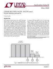
medical imaging apparatus. A new low voltage reference,<br />
the LTC6655, has only 0.3ppm (775nV) noise at 2.5VOUT.<br />
Figure 1 lists salient specifi cations in tabular form. Accuracy<br />
and temperature coeffi cient are characteristic of<br />
high grade, low voltage references. 0.1Hz to 10Hz noise,<br />
particularly noteworthy, is unequalled by any low voltage<br />
electronic reference.<br />
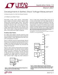
Noise Measurement<br />
Special techniques are required to verify the LTC6655’s extremely<br />
low noise. Figure 2’s approach appears innocently<br />
straightforward but practical implementation represents a<br />
high order diffi culty measurement. This 0.1Hz to 10Hz noise<br />
Application Note 124<br />
775 Nanovolt Noise Measurement for A Low Noise<br />
Voltage Reference<br />
Quantifying Silence<br />
Jim Williams<br />
July 2009<br />
testing scheme includes a low noise pre-amplifi er, fi lters<br />
and a peak-to-peak noise detector. The pre-amplifi ers 160nV<br />
noise fl oor, enabling accurate measurement, requires<br />
special design and layout techniques. A forward gain of<br />
106 permits readout by conventional instruments.<br />
Figure 3’s detailed schematic reveals some considerations<br />
required to achieve the 160nV noise fl oor. The references<br />
DC potential is stripped by the 1300μF, 1.2k resistor<br />
combination; AC content is fed to Q1. Q1-Q2, extraordinarily<br />
low noise J-FET’s, are DC stabilized by A1, with A2<br />
providing a single-ended output. Resistive feedback from<br />
A2 stabilizes the confi guration at a gain of 10,000. A2’s<br />
output is routed to amplifi er-fi lter A3-A4 which provides<br />
0.1Hz to 10Hz response at a gain of 100. A5-A8 comprise<br />
a peak-to-peak noise detector read out by a DVM at a<br />
scale factor of 1 volt/microvolt. The peak-to-peak noise<br />
detector provides high accuracy measurement, eliminating<br />
tedious interpretation of an oscilloscope display. Instantaneous<br />
noise value is supplied by the indicated output to a<br />
monitoring oscilloscope. The 74C221 one-shot, triggered<br />
by the oscilloscope sweep gate, resets the peak-to-peak<br />
noise detector at the end of each oscilloscope 10-second<br />
sweep.<br />
L, LT, LTC, LTM, <strong>Linear</strong> <strong>Technology</strong> and the <strong>Linear</strong> logo are registered trademarks of <strong>Linear</strong><br />
<strong>Technology</strong> Corporation. All other trademarks are the property of their respective owners.<br />
LTC6655 Reference Tabular Specifi cations<br />
SPECIFICATION LIMITS<br />
Output Voltages 1.250, 2.048, 2.500, 3.000, 3.300, 4.096, 5.000<br />
Initial Accuracy 0.025%, 0.05%<br />
Temperature Coeffi cient 2ppm/°C, 5ppm/°C<br />
0.1Hz to 10Hz Noise 0.775μV at VOUT = 2.500V, Peak-to-Peak Noise is within this Figure in 90% of 1000 Ten Second Measurement Intervals<br />
Additional Characteristics 5ppm/Volt Line Regulation, 500mV Dropout, Shutdown Pin, ISUPPLY = 5mA, VIN = VO + 0.5V to 13.2VMAX,<br />
IOUT(SINK/SOURCE) = ±5mA, ISHORT Circuit = 15mA.<br />
Figure 1. LTC6655 Accuracy and Temperature Coeffi cient Are Characteristic of High Grade, Low Voltage References.<br />
0.1Hz to 10Hz Noise, Particularly Noteworthy, Is Unequalled by Any Low Voltage Electronic Reference<br />
an124f<br />
<strong>AN124</strong>-1
Application Note 124<br />
Numerous details contribute to the circuit’s performance.<br />
The 1300μF capacitor, a highly specialized type, is selected<br />
for leakage in accordance with the procedure given in<br />
Appendix B. Further, it, and its associated low noise 1.2k<br />
resistor, are fully shielded against pick-up. FETs Q1 and<br />
Q2 differentially feed A2, forming a simple low noise op<br />
amp. Feedback, provided by the 100k - 10Ω pair, sets<br />
closed loop gain at 10,000. Although Q1 and Q2 have<br />
extraordinarily low noise characteristics, their offset and<br />
drift are uncontrolled. A1 corrects these defi ciencies by<br />
adjusting Q1’s channel current via Q3 to minimize the<br />
Q1-Q2 input difference. Q1’s skewed drain values ensure<br />
that A1 is able to capture the offset. A1 and Q3 supply<br />
whatever current is required into Q1’s channel to force<br />
offset within about 30μV. The FETs’ VGS can vary over<br />
a 4:1 range. Because of this, they must be selected for<br />
10% VGS matching. This matching allows A1 to capture<br />
the offset without introducing signifi cant noise. Q1 and<br />
Q2 are thermally mated and lagged in epoxy at a time<br />
constant much greater than A1’s DC stabilizing loop rolloff,<br />
preventing offset instability and hunting. The entire<br />
A1-Q1-Q2-A2 assembly and the reference under test are<br />
completely enclosed within a shielded can. 1 The reference<br />
is powered by a 9V battery to minimize noise and insure<br />
freedom from ground loops.<br />
Peak-to-peak detector design considerations include J-FET’s<br />
used as peak trapping diodes to obtain lower leakage than<br />
<strong>AN124</strong>-2<br />
LTC6655<br />
2.5V REFERENCE<br />
LOW NOISE<br />
AC PRE-AMP<br />
EN, 0.1Hz TO 10Hz = 160nV<br />
A = 10,000<br />
≈700nV<br />
NOISE<br />
0.1Hz TO 10Hz<br />
VERTICAL<br />
INPUT<br />
A = 10 6<br />
0.1Hz TO 10Hz FILTER AND<br />
PEAK TO PEAK NOISE DETECTOR<br />
0μV TO 1μV = 0V TO 1V, A = 100<br />
OUTPUT<br />
OSCILLOSCOPE<br />
<strong>AN124</strong> F02<br />
SWEEP<br />
GATE OUT<br />
DC OUT<br />
0V TO 1V = 0μVP-P TO<br />
1μVP-P AT INPUT<br />
Figure 2. Conceptual 0.1Hz to 10Hz Noise Testing Scheme Includes Low Noise Pre-Amplifi er, Filter and Peak to Peak Noise<br />
Detector. Pre-Amplifi er’s 160nV Noise Floor, Enabling Accurate Measurement, Requires Special Design and Layout Techniques<br />
RESET<br />
afforded by conventional diodes. Diodes at the FET gates<br />
clamp reverse voltage, further minimizing leakage. 2 The peak<br />
storage capacitors highly asymmetric charge-discharge<br />
profi le necessitates the low dielectric absorption polypropelene<br />
capacitors specifi ed. 3 Oscilloscope connections via<br />
galvanically isolated links prevent ground loop induced<br />
corruption. The oscilloscope input signal is supplied by an<br />
isolated probe; the sweep gate output is interfaced with an<br />
isolation pulse transformer. Details appear in Appendix C.<br />
Noise Measurement Circuit Performance<br />
Circuit performance must be characterized prior to measuring<br />
LTC6655 noise. The pre-amplifi er stage is verifi ed<br />
for >10Hz bandwidth by applying a 1μV step at its input<br />
(reference disconnected) and monitoring A2’s output.<br />
Figure 4’s 10ms risetime indicates 35Hz response, insuring<br />
the entire 0.1Hz to 10Hz noise spectrum is supplied to the<br />
succeeding fi lter stage.<br />
Note 1. The pre-amplifi er structure must be carefully prepared. See<br />
Appendix A, “Mechanical and Layout Considerations”, for detail on preamplifi<br />
er construction.<br />
Note 2. Diode connected J-FET’s superior leakage derives from their<br />
extremely small area gate-channel junction. In general, J-FET’s leak a few<br />
picoamperes (25°C) while common signal diodes (e.g. 1N4148) are about<br />
1,000X worse (units of nanoamperes at 25°C).<br />
Note 3. Tefl on and polystyrene dielectrics are even better but the Real<br />
World intrudes. Tefl on is expensive and excessively large at 1μF. Analog<br />
types mourn the imminent passing of the polystyrene era as the sole<br />
manufacturer of polystyrene fi lm has ceased production.<br />
an124f
0.1μF<br />
1N4697<br />
10V<br />
0.15μF<br />
15V<br />
A = 100 AND<br />
0.1Hz TO 10Hz FILTER<br />
10k<br />
+<br />
1μF A1<br />
LT1012<br />
–<br />
–<br />
A4<br />
LT1012<br />
0.1μF<br />
2k<br />
15V<br />
1k* 200Ω*<br />
Q3<br />
2N2907<br />
–15V<br />
+<br />
124k* 124k*<br />
+<br />
A3<br />
LT1012<br />
1μF<br />
–15V<br />
A = 10 4<br />
LOW NOISE<br />
PRE-AMP<br />
0.1μF<br />
–<br />
450Ω* 900Ω*<br />
–<br />
A2<br />
LT1097<br />
+<br />
5<br />
Q1 Q2 0.022μF<br />
1μF<br />
+<br />
1M*<br />
330μF<br />
16V<br />
9V<br />
100k<br />
100k<br />
10k*<br />
330μF<br />
16V<br />
1300μF<br />
SHIELD<br />
T<br />
+<br />
100Ω*<br />
330Ω*<br />
100k*<br />
+<br />
S<br />
F<br />
LTC6655<br />
2.5V<br />
**1.2k<br />
IN<br />
SD<br />
10k<br />
IN OUT<br />
– INPUT<br />
ROOT-SUM-SQUARE<br />
CORRECTION<br />
SEE TEXT<br />
+<br />
330μF<br />
16V<br />
330μF<br />
16V<br />
10Ω*<br />
750Ω*<br />
1μF<br />
–15V<br />
REFERENCE<br />
UNDER TEST<br />
+<br />
SHIELDED CAN<br />
AC LINE GROUND<br />
RESET PULSE<br />
GENERATOR<br />
+15<br />
PEAK TO PEAK<br />
NOISE DETECTOR<br />
4.7k<br />
BAT-85<br />
B2<br />
0.22μF<br />
10k<br />
+15<br />
C2 RC2<br />
RST = Q2 +V<br />
74C221<br />
+<br />
A7<br />
1/4 LT1058<br />
+ PEAK<br />
–<br />
A5<br />
1/4 LT1058<br />
1μF<br />
RST<br />
BAT-85<br />
P<br />
–<br />
+<br />
1k<br />
+15<br />
10k<br />
A2<br />
CLR2<br />
+15<br />
10k<br />
Application Note 124<br />
TO OSCILLOSCOPE INPUT<br />
VIA ISOLATED PROBE,<br />
1V/DIV = 1μV/DIV,<br />
REFERRED TO INPUT,<br />
SWEEP = 1s/DIV<br />
+<br />
–15<br />
FROM OSCILLOSCOPE<br />
SWEEP GATE OUTPUT<br />
VIA ISOLATION<br />
PULSE TRANSFORMER<br />
O TO 1V =<br />
O TO 1μV<br />
DVM<br />
–<br />
0.1μF<br />
0.005μF<br />
100k<br />
1k<br />
* = 1% METAL FILM<br />
** = 1% WIREWOUND, ULTRONIX105A<br />
= TANTALUM,WET SLUG<br />
ILEAK < 5nA<br />
SEE TEXT/APPENDIX B<br />
Q1, Q2 = THERMALLY MATED<br />
2SK369 (MATCH VGS 10%)<br />
OR LSK389 DUAL<br />
THERMALLY LAG<br />
SEE TEXT<br />
+<br />
A8<br />
1/4 LT1058<br />
4.7k<br />
– PEAK<br />
T<br />
= 1N4148<br />
–<br />
–<br />
A6<br />
1/4 LT1058<br />
100k<br />
P<br />
1μF<br />
RST<br />
= POLYPROPELENE<br />
P<br />
= 2N4393<br />
+<br />
A4 330μF OUTPUT CAPACITORS =
Application Note 124<br />
Figure 5 describes peak-to-peak noise detector operation.<br />
Waveforms include A3’s input noise signal (Trace A), A7<br />
(Trace B) positive/A8 (Trace C) negative peak detector<br />
outputs and DVM differential input (Trace D). Trace E’s<br />
oscilloscope supplied reset pulse has been lengthened<br />
for photographic clarity.<br />
Circuit noise fl oor is measured by replacing the LTC6655<br />
with a 3V battery stack. Dielectric absorption effects in<br />
the large input capacitor require a 24-hour settling period<br />
before measurement. Figure 6, taken at the circuit’s oscilloscope<br />
output, shows 160nV 0.1Hz to 10Hz noise in a<br />
10 second sample window. Because noise adds in rootsum-square<br />
fashion, this represents about a 2% error in<br />
2mV/DIV<br />
<strong>AN124</strong>-4<br />
10ms/DIV<br />
<strong>AN124</strong> F04<br />
Figure 4. Pre-Amplifi er Rise Time Measures 10ms; Indicated<br />
35Hz Bandwidth Ensures Entire 0.1Hz to 10Hz Noise Spectrum Is<br />
Supplied to Succeeding Filter Stage<br />
A = 5mV/DIV<br />
B = 0.5V/DIV<br />
C = 0.5V/DIV<br />
D = 1V/DIV<br />
E = 20V/DIV<br />
1s/DIV<br />
<strong>AN124</strong> F05<br />
Figure 5. Waveforms for Peak to Peak Noise Detector Include<br />
A3 Input Noise Signal (Trace A), A7 (Trace B) Positive/A8<br />
(Trace C) Negative Peak Detector Outputs and DVM Differential<br />
Input (Trace D). Trace E’s Oscilloscope Supplied Reset Pulse<br />
Lengthened for Photographic Clarity<br />
100nV/DIV<br />
1s/DIV<br />
<strong>AN124</strong> F06<br />
Figure 6. Low Noise Circuit/Layout Techniques Yield 160nV<br />
0.1Hz to 10Hz Noise Floor, Ensuring Accurate Measurement.<br />
Photograph Taken at Figure 3’s Oscilloscope Output with 3V<br />
Battery Replacing LTC6655 Reference. Noise Floor Adds ≈2%<br />
Error to Expected LTC6655 Noise Figure Due to Root-Sum-Square<br />
Noise Addition Characteristic; Correction is Implemented at<br />
Figure 3’s A3<br />
the LTC 6655’s expected 775nV noise fi gure. This term is<br />
accounted for by placing Figure 3’s “root-sum-square correction”<br />
switch in the appropriate position during reference<br />
testing. The resultant 2% gain attenuation fi rst order corrects<br />
LTC6655 output noise reading for the circuit’s 160nV<br />
noise fl oor contribution. Figure 7, a strip-chart recording<br />
of the peak-to-peak noise detector output over 6 minutes,<br />
shows less than 160nV test circuit noise. 4 Resets occur<br />
every 10 seconds. A 3V battery biases the input capacitor,<br />
replacing the LTC6655 for this test.<br />
Figure 8 is LTC6655 noise after the indicated 24-hour<br />
dielectric absorption soak time. Noise is within 775nV<br />
peak-to-peak in this 10 second sample window with<br />
the root-sum-square correction enabled. The verifi ed,<br />
extremely low circuit noise fl oor makes it highly likely<br />
this data is valid. In closing, it is worth mention that the<br />
approach taken is applicable to measuring any 0.1Hz to<br />
10Hz noise source, although the root-sum-square error<br />
correction coeffi cient should be re-established for any<br />
given noise level.<br />
Note 4. That’s right, a strip-chart recording. Stubborn, locally based<br />
aberrants persist in their use of such archaic devices, forsaking more<br />
modern alternatives. Technical advantage could account for this choice,<br />
although deeply seated cultural bias may be indicated.<br />
an124f
AMPLITUDE<br />
100nV<br />
0V<br />
1 MIN<br />
TIME<br />
<strong>AN124</strong> F07<br />
Figure 7. Peak to Peak Noise Detector Output Observed Over<br />
6 Minutes Shows
Application Note 124<br />
APPENDIX A<br />
Mechanical and Layout Considerations<br />
The low noise X10,000 preamplifi er, crucial to the noise<br />
measurement, must be quite carefully prepared. Figure<br />
A1 shows board layout. The board is enclosed within<br />
a shielded can, visible in A1A. Additional shielding is<br />
provided to the input capacitor and resistor (A1A left);<br />
the resistor’s wirewound construction has low noise but<br />
is particularly susceptible to stray fi elds. A1A also shows<br />
the socketed LTC6655 reference under test (below the<br />
large input capacitor shield) and the JFET input amplifi er<br />
associated components. Q3 (A1A upper right), a heat<br />
source, is located away from the JFET printed circuit lands,<br />
Figure A1. Preamplifi er Board Top (Figure A1A) and Bottom (A1B) Views. Board Top Includes Shielded Input Capacitor (Upper Left)<br />
and Input Resistor (Upper Center Left). Stabilized JFET Input Amplifi er Occupies Board Upper Center Right; Output Stage Adjoins<br />
BNC Fitting. Reference Under Test Resides in Socket Below Input Capacitor. ±15 Power Enters Shielded Enclosure Via Banana Jacks<br />
(Extreme Right). 9V Battery (Lower) Supplies Reference Under Test. Board Bottom’s Epoxy Filled Plastic Cup (A1B Center) Contains<br />
JFETs, Provides Thermal Mating and Lag<br />
<strong>AN124</strong>-6<br />
preventing convection currents from introducing noise.<br />
Additionally, the JFET’s are contained within an epoxy fi lled<br />
plastic cup (Figure A1B center), promoting thermal mating<br />
and lag. 1 This thermal management of the FETs prevents<br />
offset instability and hunting in A1’s stabilizing loop from<br />
masquerading as low frequency noise. ±15V power enters<br />
the enclosure via banana jacks; the reference is supplied<br />
by a 9V battery (both visible in A1A). The A = 100 fi lter<br />
and peak-peak detector circuitry occupies a separate board<br />
outside the shielded can. No special commentary applies to<br />
this section although board leakage to the peak detecting<br />
capacitors should be minimized with guard rings or fl ying<br />
lead/Tefl on stand-off construction.<br />
Note 1. The plastic cup, supplied by Martinelli and Company, also<br />
includes, at no charge, 10 ounces of apple juice.<br />
Figure A1A. Figure A1B.<br />
an124f
APPENDIX B<br />
Input Capacitor Selection Procedure<br />
The input capacitor, a highly specialized type, must be<br />
selected for leakage. If this is not done, resultant errors<br />
can saturate the input pre-amplifi er or introduce noise.<br />
The highest grade wet slug 200°C rated tantalum capacitors<br />
are utilized. The capacitor operates at a small fraction<br />
of its rated voltage at room temperature, resulting<br />
in much lower leakage than its specifi cation indicates.<br />
3V<br />
AA<br />
CELLS<br />
1.5V<br />
1.5V<br />
VISHAY<br />
XTV138M030P0A<br />
WET SLUG TANTALUM<br />
+ 1300μF/30V –<br />
1k<br />
hp<br />
TEST SEQUENCE<br />
1. TURN OFF MICROVOLT METER<br />
2. CONNECT 3V BATTERY STACK<br />
3. WAIT 24 HOURS<br />
4. TURN ON MICROVOLT METER<br />
5. READ CAPACITOR LEAKAGE, 1nA = 1μV<br />
+ –<br />
Application Note 124<br />
The capacitor’s dielectric absorption requires a 24-hour<br />
charge time to insure meaningful measurement. Capacitor<br />
leakage is determined by following the 5-step procedure<br />
given in the fi gure. Yield to required 5-nanoampere leakage<br />
exceeds 90%. 1<br />
Note 1. This high yield is most welcome because the specifi ed capacitors<br />
are spectacularly priced at almost $400.00. There may be a more palatable<br />
alternative. Selected commercial grade aluminum electrolytics can<br />
approach the required DC leakage although their aperiodic noise bursts<br />
(mechanism not understood; reader comments invited) are a concern.<br />
HP-419A MICROVOLT METER<br />
Figure B1. Pre-Amplifi er Input Capacitor Selected for
Application Note 124<br />
APPENDIX C<br />
Power, Grounding and Shielding Considerations<br />
Figure 3’s circuit requires great care in power distribution,<br />
grounding and shielding to achieve the reported results.<br />
Figure C1 depicts an appropriate scheme. A low shunt capacitance<br />
line isolation transformer powers an instrument<br />
grade ±15V supply, furnishing clean, low noise power. The<br />
pre-amplifi er’s shielded can is tied to the 110V AC ground<br />
terminal, directing pick-up to earth ground. Filter/peak-topeak<br />
detector oscilloscope connections are made via an<br />
isolated probe and a pulse isolation transformer, precluding<br />
error inducing ground loops. 1 The indicated loop, included<br />
to verify no current fl ow between circuit common and earth<br />
ground, is monitored with a current probe. Figures C2 and<br />
C3, both optional, show battery powered supplies which<br />
replace the line isolation transformer and instrumentation<br />
9V<br />
BATTERY<br />
SHIELDED CAN<br />
<strong>AN124</strong>-8<br />
= AC LINE GROUND<br />
= CIRCUIT COMMON<br />
REFERENCE<br />
UNDER TEST<br />
A = 10,000<br />
PRE-AMP<br />
RF<br />
FEEDTHROUGHS<br />
HEWLETT PACKARD,<br />
6111A,<br />
PHILBRICK RESEARCHES<br />
6033, PR-300<br />
TEKTRONIX A6909,<br />
TEKTRONIX A6902B,<br />
SIGNAL ACQUISITION<br />
TECHNOLOGIES SL-10<br />
+15<br />
–15<br />
INSTRUMENT<br />
GRADE ±15V<br />
POWER SUPPLY<br />
grade power supplies. C2 uses linear regulators to furnish<br />
low noise ±15V. Because the batteries fl oat, positive<br />
regulators suffi ce for both positive and negative rails. In<br />
C3, a single battery stack supplies an extremely low noise<br />
DC-DC converter to furnish positive and negative rails via<br />
low noise discrete linear regulators. 2 Both of these battery<br />
supplied approaches are economical compared to the AC<br />
line powered version but require battery maintenance.<br />
The indicated commercial products accompanying<br />
Figure C1’s blocks represent typical applicable units which<br />
have been found to satisfy requirements. Other types<br />
may be employed but should be verifi ed for necessary<br />
performance.<br />
Note 1. An acceptable alternative to the isolated probe is monitoring<br />
Figure 3’s A4 output current into a grounded 1k resistor with a DC<br />
stabilized current probe (e.g. Tektronix P6042, AM503). The resultant<br />
isolated 1V/μV oscilloscope presentation requires 10Hz lowpass fi ltering<br />
(see Appendix D) due to inherent current probe noise.<br />
Note 2. References 6 and 8 detail the specialized DC-DC converter used.<br />
OSCILLOSCOPE<br />
VERTICAL<br />
INPUT<br />
ISOLATED<br />
PROBE<br />
A = 100<br />
FILTER AND<br />
PEAK TO PEAK<br />
DETECTOR<br />
CIRCUIT<br />
COMMON<br />
PEAK TO PEAK<br />
RESET<br />
+<br />
DVM<br />
–<br />
SWEEP RESET<br />
PULSE ISOLATION<br />
TRANSFORMER/<br />
COAXIAL CAPACITOR<br />
TOPAZ, 0111T35S<br />
LOW SHUNT<br />
CAPACITANCE ISOLATION<br />
TRANSFORMER<br />
(LOCATE ≥3 FEET<br />
FROM SHIELDED CAN)<br />
CURRENT<br />
MONITOR<br />
LOOP<br />
DEERFIELD LAB 185,<br />
HEWLETT PACKARD<br />
10240B<br />
110VAC<br />
LINE INPUT<br />
Figure C1. Power/Grounding/Shielding Scheme for Low Noise Measurement Minimizes AC Line Originated Interference<br />
and Mixing of Circuit Return and AC Line Ground Current. No Current Should Flow in Current Monitor Loop<br />
<strong>AN124</strong> FC1<br />
an124f
12 Size D<br />
ALKALINE<br />
1.5V CELLS<br />
EACH PACK<br />
+18<br />
+<br />
+<br />
10μF<br />
10μF<br />
* = 1% METAL FILM RESISTOR<br />
SD B<br />
IN LT1761 OUT<br />
Application Note 124<br />
Figure C2. LT1761 Regulators form ±15V, Low Noise Power Supply. Isolated Battery Packs Permit Positive<br />
Regulator to Supply Negative Output and Eliminate Possible AC Line Referred Ground Loops<br />
FB<br />
SD B<br />
IN LT1761 OUT<br />
FB<br />
0.1μF<br />
13.7k*<br />
1.21k*<br />
0.1μF<br />
13.7k*<br />
1.21k*<br />
<strong>AN124</strong> FC2<br />
+<br />
+<br />
+15<br />
10μF<br />
–15<br />
10μF<br />
an124f<br />
<strong>AN124</strong>-9
Application Note 124<br />
6V BATTERY<br />
4x 1.5V<br />
ALKALINE<br />
D CELL<br />
6V<br />
V IN<br />
+<br />
<strong>AN124</strong>-10<br />
4.7μF<br />
GND FB CT RT 9<br />
8<br />
3300pF<br />
10k<br />
RVSL<br />
15k<br />
14 13 12<br />
43k<br />
5V<br />
LT1533<br />
5<br />
15k<br />
RCSL DUTY<br />
6<br />
3 2<br />
COL A<br />
PGND COL B<br />
16<br />
18k L1<br />
L1: 22nH INDUCTOR. COILCRAFT B-07T TYPICAL,<br />
PC TRACE, OR FERRITE BEAD<br />
L2, L3: PULSE ENGINEERING. PE92100<br />
T1: COILTRONICS CTX-02-13664-X1<br />
: 1N4148<br />
* = 1% METAL FILM<br />
15<br />
6V<br />
2 T1<br />
12<br />
3 10<br />
4 9<br />
4.7μF<br />
5<br />
7<br />
+<br />
+<br />
100μF<br />
–<br />
4<br />
1/2 LT1013<br />
10k*<br />
+<br />
1μF<br />
100μF<br />
–19V UNREGULATED<br />
5k<br />
–<br />
1/2 LT1013<br />
+<br />
8<br />
19V UNREGULATED<br />
Figure C3. A Low Noise, Bipolar, Floating Output Converter. Grounding LT1533 “DUTY” Pin and Biasing FB Puts Regulator into 50%<br />
Duty Cycle Mode. LT1533’s Controlled Transition Times Permit
APPENDIX D<br />
High Sensitivity, Low Noise Amplifi ers<br />
Figure D1 lists some useful low level amplifi ers for setting<br />
up and troubleshooting the texts’ circuit. The table lists<br />
both oscilloscope plug-in amplifi ers and stand-alone types.<br />
Two major restrictions apply. The fi lters in these units<br />
INSTRUMENT<br />
TYPE MANUFACTURER<br />
MODEL<br />
NUMBER<br />
–3dB<br />
BANDWIDTH<br />
MANUFACTURER MODEL NUMBER MODIFICATION<br />
Tektronix 1A7 Parallel C370A with 1μF<br />
Tektronix 1A7A Parallel C445A with 1μF<br />
Tektronix 7A22 Parallel C426H with 3μF<br />
Tektronix AM502 Parallel C449 with 3μF<br />
Figure D2. Modifi cation Information for Various Tektronix Low<br />
Level Oscilloscope Plug-In’s and Amplifi ers Permits 10Hz High<br />
Frequency Filter Operation in 100Hz Panel Switch Position. All<br />
Cases Utilize 100V, Mylar Capacitors<br />
Information furnished by <strong>Linear</strong> <strong>Technology</strong> Corporation is believed to be accurate and reliable.<br />
However, no responsibility is assumed for its use. <strong>Linear</strong> <strong>Technology</strong> Corporation makes no representation<br />
that the interconnection of its circuits as described herein will not infringe on existing patent rights.<br />
Application Note 124<br />
MAXIMUM<br />
SENSITIVITY/GAIN AVAILABILITY COMMENTS<br />
Differential Amplifi er Tektronix 1A7/1A7A 1MHz 10μV/DIV Secondary Market Requires 500 Series Mainframe,<br />
Settable Bandstops<br />
Differential Amplifi er Tektronix 7A22 1MHz 10μV/DIV Secondary Market Requires 7000 Series Mainframe,<br />
Settable Bandstops<br />
Differential Amplifi er Tektronix 5A22 1MHz 10μV/DIV Secondary Market Requires 5000 Series Mainframe,<br />
Settable Bandstops<br />
Differential Amplifi er Tektronix ADA-400A 1MHz 10μV/DIV Current Production Stand-Alone with Optional Power<br />
Supply, Settable Bandstops<br />
Differential Amplifi er Preamble 1822 10MHz Gain = 1000 Current Production Stand-Alone, Settable Bandstops<br />
Differential Amplifi er Stanford<br />
Research<br />
Systems<br />
are single-pole types resulting in somewhat pessimistic<br />
bandwidth cut-offs. Additionally, the amplifi ers listed do<br />
not include 10Hz lowpass frequency fi lters, although<br />
they are easily modifi ed to provide this capability. Figure<br />
D2 lists four amplifi ers with the necessary modifi cation<br />
information. 1<br />
Note 1. See References 14-17.<br />
SR-560 1MHz Gain = 50000 Current Production Stand-Alone, Settable Bandstops,<br />
Battery or Line Operation<br />
Differential Amplifi er Tektronix AM-502 1MHz Gain = 100000 Secondary Market Requires TM-500 Series Power<br />
Supply, Settable Bandstops<br />
Figure D1. Some Useful High Sensitivity, Low Noise Amplifi ers. Trade-Offs Include Bandwidth, Sensitivity and Availability<br />
an124f<br />
<strong>AN124</strong>-11
Application Note 124<br />
<strong>AN124</strong>-12<br />
500nV/DIV<br />
1s/DIV<br />
<strong>Linear</strong> <strong>Technology</strong> Corporation<br />
1630 McCarthy Blvd., Milpitas, CA 95035-7417<br />
(408) 432-1900 ● FAX: (408) 434-0507 ● LT 0709 • PRINTED IN USA<br />
www.linear.com © LINEAR TECHNOLOGY CORPORATION 2009<br />
<strong>AN124</strong> QT<br />
an124f