AN124 - Linear Technology
AN124 - Linear Technology
AN124 - Linear Technology

Create successful ePaper yourself
Turn your PDF publications into a flip-book with our unique Google optimized e-Paper software.
Application Note 124<br />
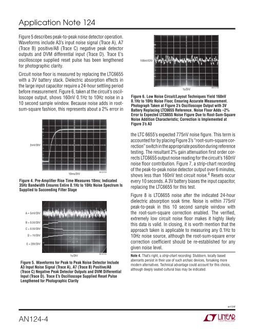
Figure 5 describes peak-to-peak noise detector operation.<br />
Waveforms include A3’s input noise signal (Trace A), A7<br />
(Trace B) positive/A8 (Trace C) negative peak detector<br />
outputs and DVM differential input (Trace D). Trace E’s<br />
oscilloscope supplied reset pulse has been lengthened<br />
for photographic clarity.<br />
Circuit noise fl oor is measured by replacing the LTC6655<br />
with a 3V battery stack. Dielectric absorption effects in<br />
the large input capacitor require a 24-hour settling period<br />
before measurement. Figure 6, taken at the circuit’s oscilloscope<br />
output, shows 160nV 0.1Hz to 10Hz noise in a<br />
10 second sample window. Because noise adds in rootsum-square<br />
fashion, this represents about a 2% error in<br />
2mV/DIV<br />
<strong>AN124</strong>-4<br />
10ms/DIV<br />
<strong>AN124</strong> F04<br />
Figure 4. Pre-Amplifi er Rise Time Measures 10ms; Indicated<br />
35Hz Bandwidth Ensures Entire 0.1Hz to 10Hz Noise Spectrum Is<br />
Supplied to Succeeding Filter Stage<br />
A = 5mV/DIV<br />
B = 0.5V/DIV<br />
C = 0.5V/DIV<br />
D = 1V/DIV<br />
E = 20V/DIV<br />
1s/DIV<br />
<strong>AN124</strong> F05<br />
Figure 5. Waveforms for Peak to Peak Noise Detector Include<br />
A3 Input Noise Signal (Trace A), A7 (Trace B) Positive/A8<br />
(Trace C) Negative Peak Detector Outputs and DVM Differential<br />
Input (Trace D). Trace E’s Oscilloscope Supplied Reset Pulse<br />
Lengthened for Photographic Clarity<br />
100nV/DIV<br />
1s/DIV<br />
<strong>AN124</strong> F06<br />
Figure 6. Low Noise Circuit/Layout Techniques Yield 160nV<br />
0.1Hz to 10Hz Noise Floor, Ensuring Accurate Measurement.<br />
Photograph Taken at Figure 3’s Oscilloscope Output with 3V<br />
Battery Replacing LTC6655 Reference. Noise Floor Adds ≈2%<br />
Error to Expected LTC6655 Noise Figure Due to Root-Sum-Square<br />
Noise Addition Characteristic; Correction is Implemented at<br />
Figure 3’s A3<br />
the LTC 6655’s expected 775nV noise fi gure. This term is<br />
accounted for by placing Figure 3’s “root-sum-square correction”<br />
switch in the appropriate position during reference<br />
testing. The resultant 2% gain attenuation fi rst order corrects<br />
LTC6655 output noise reading for the circuit’s 160nV<br />
noise fl oor contribution. Figure 7, a strip-chart recording<br />
of the peak-to-peak noise detector output over 6 minutes,<br />
shows less than 160nV test circuit noise. 4 Resets occur<br />
every 10 seconds. A 3V battery biases the input capacitor,<br />
replacing the LTC6655 for this test.<br />
Figure 8 is LTC6655 noise after the indicated 24-hour<br />
dielectric absorption soak time. Noise is within 775nV<br />
peak-to-peak in this 10 second sample window with<br />
the root-sum-square correction enabled. The verifi ed,<br />
extremely low circuit noise fl oor makes it highly likely<br />
this data is valid. In closing, it is worth mention that the<br />
approach taken is applicable to measuring any 0.1Hz to<br />
10Hz noise source, although the root-sum-square error<br />
correction coeffi cient should be re-established for any<br />
given noise level.<br />
Note 4. That’s right, a strip-chart recording. Stubborn, locally based<br />
aberrants persist in their use of such archaic devices, forsaking more<br />
modern alternatives. Technical advantage could account for this choice,<br />
although deeply seated cultural bias may be indicated.<br />
an124f