Endoscope Quick Reference Guide - Texas Instruments
Endoscope Quick Reference Guide - Texas Instruments
Endoscope Quick Reference Guide - Texas Instruments

Create successful ePaper yourself
Turn your PDF publications into a flip-book with our unique Google optimized e-Paper software.
<strong>Endoscope</strong>s <strong>Quick</strong> <strong>Reference</strong> <strong>Guide</strong><br />
➔<br />
<strong>Endoscope</strong> Solutions<br />
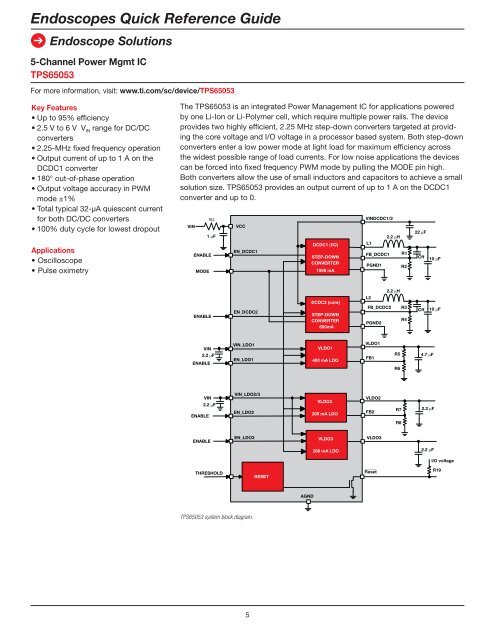
5-Channel Power Mgmt IC<br />
TPS65053<br />
For more information, visit: www.ti.com/sc/device/TPS65053<br />
Key Features<br />
• Up to 95% efficiency<br />
• 2.5 V to 6 V V IN range for DC/DC<br />
converters<br />
• 2.25-MHz fixed frequency operation<br />
• Output current of up to 1 A on the<br />
DCDC1 converter<br />
• 180° out-of-phase operation<br />
• Output voltage accuracy in PWM<br />
mode ±1%<br />
• Total typical 32-µA quiescent current<br />
for both DC/DC converters<br />
• 100% duty cycle for lowest dropout<br />
Applications<br />
• Oscilloscope<br />
• Pulse oximetry<br />
The TPS65053 is an integrated Power Management IC for applications powered<br />
by one Li-Ion or Li-Polymer cell, which require multiple power rails. The device<br />
provides two highly efficient, 2.25 MHz step-down converters targeted at providing<br />
the core voltage and I/O voltage in a processor based system. Both step-down<br />
converters enter a low power mode at light load for maximum efficiency across<br />
the widest possible range of load currents. For low noise applications the devices<br />
can be forced into fixed frequency PWM mode by pulling the MODE pin high.<br />
Both converters allow the use of small inductors and capacitors to achieve a small<br />
solution size. TPS65053 provides an output current of up to 1 A on the DCDC1<br />
converter and up to 0.<br />
VIN<br />
ENABLE<br />
MODE<br />
ENABLE<br />
VIN<br />
2.2 F<br />
ENABLE<br />
ENABLE<br />
1<br />
1 F<br />
VIN<br />
2.2 F<br />
ENABLE<br />
THRESHOLD<br />
VCC<br />
EN_DCDC1<br />
EN_DCDC2<br />
VIN_LDO1<br />
EN_LDO1<br />
VIN_LDO2/3<br />
EN_LDO2<br />
EN_LDO3<br />
TPS65053 system block diagram.<br />
5<br />
RESET<br />
AGND<br />
STEP-DOWN<br />
CONVERTER<br />
STEP-DOWN<br />
CONVERTER<br />
600mA<br />
VLDO1<br />
VLDO2<br />
VLDO3<br />
VINDCDC1/2<br />
L1<br />
FB_DCDC1<br />
PGND1<br />
L2<br />
FB_DCDC2<br />
PGND2<br />
VLDO1<br />
FB1<br />
VLDO2<br />
FB2<br />
VLDO3<br />
Reset<br />
2.2 H<br />
2.2 H<br />
R5<br />
R6<br />
R7<br />
R8<br />
R1<br />
R2<br />
R3<br />
R4<br />
22 F<br />
Cff<br />
Cff<br />
4.7 F<br />
2.2 F<br />
2.2 F<br />
10 F<br />
10 F<br />
R19