MIB High Impedance Bus Differential Relay - GE Digital Energy
MIB High Impedance Bus Differential Relay - GE Digital Energy
MIB High Impedance Bus Differential Relay - GE Digital Energy

You also want an ePaper? Increase the reach of your titles
YUMPU automatically turns print PDFs into web optimized ePapers that Google loves.
g<br />
<strong>GE</strong> Multilin<br />
215 Anderson Avenue<br />
L6E 1B3 Markham, ON -CANADA<br />
T (905) 294 6222 F (905) 294 8512<br />
E gemultilin@ge.com<br />
Internet: www.<strong>GE</strong>Multilin.com<br />
<strong>GE</strong> Consumer & Industrial<br />
Multilin<br />
<strong>MIB</strong><br />
<strong>High</strong> <strong>Impedance</strong> <strong>Bus</strong> <strong>Differential</strong><br />
<strong>Relay</strong><br />
Instruction manual<br />
<strong>GE</strong>K-106426D<br />
Copyright © 2008 <strong>GE</strong> Multilin<br />
<strong>GE</strong> Multilin<br />
Avda. Pinoa, 10<br />
48170 Zamudio SPAIN<br />
T +34 94 485 88 00 F +34 94 485 88 45<br />
E gemultilin.euro@ge.com
TABLE OF CONTENTS<br />
1. <strong>GE</strong>TTING STARTED 1.1 INSPECTION CHECKLIST<br />
1.2 ENERVISTA MII SETUP SOFTWARE<br />
1.2.1 SYSTEM REQUIREMENTS .............................................................................. 1-4<br />
1.2.2 SAFETY INSTRUCTIONS ................................................................................. 1-4<br />
1.2.3 INSTALLATION.................................................................................................. 1-5<br />
1.3 MII RELAY FAMILY HARDWARE<br />
1.3.1 MOUNTING & WIRING.................................................................................... 1-11<br />
1.3.2 COMMUNICATIONS........................................................................................ 1-11<br />
1.3.3 FACEPLATE KEYPAD & DISPLAY ................................................................. 1-11<br />
1.4 USING THE KEYPAD AND DISPLAY<br />
1.4.1 HIERARCHICAL MENUS ................................................................................ 1-13<br />
2. PRODUCT DESCRIPTION 2.1 SUMMARY<br />
2.1.1 <strong>GE</strong>NERAL OVERVIEW...................................................................................... 2-1<br />
2.2 INTRODUCTION<br />
2.3 ACCESS SECURITY FEATURES<br />
2.3.1 ........................... DIFFERENTIAL UNITSDIFFERENTIAL UNITS (87-1) (87-2)2-6<br />
2.4 CALCULATION OF SETTINGS<br />
2.4.1 SETTING OF THE DIFFERENTIAL ELEMENT................................................. 2-7<br />
2.4.2 MINIMUM FAULT TO TRIP 87 .......................................................................... 2-8<br />
2.5 EVENTS<br />
2.6 OSCILLOGRAPHY<br />
2.7 MULTIPLE SETTING GROUPS<br />
2.8 MEASUREMENT AND SELF-TEST<br />
2.8.1 MEASUREMENT ............................................................................................. 2-13<br />
2.8.2 SELF-TEST...................................................................................................... 2-13<br />
2.9 USER INTERFACE<br />
2.9.1 LED TAR<strong>GE</strong>TS ................................................................................................ 2-14<br />
2.9.2 KEYPAD AND DISPLAY.................................................................................. 2-15<br />
2.9.3 COMMUNICATION PORTS............................................................................. 2-15<br />
2.9.4 SOFTWARE..................................................................................................... 2-15<br />
2.10 ORDERING CODES<br />
2.11 TECHNICAL SPECIFICATIONS<br />
2.11.1 PROTECTION ELEMENTS ........................................................................... 2-17<br />
2.11.2 METERING FUNCTIONS ................................................................................ 2-17<br />
2.11.3 INPUTS ............................................................................................................ 2-17<br />
2.11.4 POWER SUPPLY ............................................................................................ 2-18<br />
2.11.5 OUTPUTS ........................................................................................................ 2-18<br />
2.11.6 COMMUNICATIONS........................................................................................ 2-19<br />
2.11.7 ENVIRONMENTAL .......................................................................................... 2-19<br />
2.11.8 TYPE TESTS AND CERTIFICATIONS............................................................ 2-19<br />
2.11.9 PRODUCTION TESTS .................................................................................... 2-20<br />
2.11.10 APPROVALS ................................................................................................... 2-20<br />
2.12 TECHNICAL SPECIFICATIONS FOR HID MODULE<br />
2.12.1 VOLTA<strong>GE</strong> LIMITERS....................................................................................... 2-21<br />
2.12.2 LATCHING RELAY .......................................................................................... 2-22<br />
2.12.3 ENVIRONMENTAL .......................................................................................... 2-22<br />
3. HARDWARE 3.1 DESCRIPTION<br />
3.2 HIGH IMPEDANCE MODULE DESCRIPTION<br />
3.2.1 MOUNTING........................................................................................................ 3-2<br />
3.2.2 MECHANICAL DESCRIPTION .......................................................................... 3-4<br />
<strong>GE</strong>K-106426D <strong>MIB</strong> <strong>High</strong> <strong>Impedance</strong> <strong>Bus</strong> <strong>Differential</strong> <strong>Relay</strong> 1
TABLE OF CONTENTS<br />
3.2.3 REAR DESCRIPTION ........................................................................................3-5<br />
3.2.4 TYPICAL WIRING DIAGRAM.............................................................................3-6<br />
3.2.5 CONTROL POWER............................................................................................3-7<br />
3.2.6 AC CURRENT TRANSFORMER INPUTS .........................................................3-8<br />
3.3 HIGH-SPEED OVERCURRENT PROTECTION MODULE<br />
3.3.1 MECHANICAL DESCRIPTION...........................................................................3-9<br />
3.3.2 MOUNTING ........................................................................................................3-9<br />
3.3.3 REAR DESCRIPTION ........................................................................................3-9<br />
3.3.4 CONTACT INPUTS / OUTPUTS .....................................................................3-10<br />
3.3.5 OUTPUT CONTACTS CONFIGURATION .......................................................3-11<br />
3.3.6 OUTPUTS ISOLATION ....................................................................................3-12<br />
3.3.7 RS232 FRONT COMMUNICATIONS PORT....................................................3-15<br />
3.3.8 RS485 COMMUNICATIONS PORT .................................................................3-16<br />
4. COMMUNICATIONS 4.1 ENERVISTA MII SETUP SOFTWARE<br />
4.1.1 OVERVIEW ........................................................................................................4-1<br />
4.1.2 STARTING COMMUNICATION..........................................................................4-2<br />
4.1.3<br />
4.2 FILE<br />
MAIN SCREEN...................................................................................................4-2<br />
4.2.1 NEW ...................................................................................................................4-3<br />
4.2.2 OPEN..................................................................................................................4-3<br />
4.2.3 PROPERTIES.....................................................................................................4-4<br />
4.2.4 <strong>GE</strong>T INFO FROM RELAY ..................................................................................4-4<br />
4.2.5 SEND INFO TO RELAY .....................................................................................4-4<br />
4.2.6 PRINT SETUP ....................................................................................................4-5<br />
4.2.7 PRINT PREVIEW ...............................................................................................4-5<br />
4.2.8 PRINT .................................................................................................................4-6<br />
4.2.9 CLOSE................................................................................................................4-6<br />
4.3 SETPOINT<br />
4.3.1 SETTINGS..........................................................................................................4-7<br />
4.3.2 MAIN SETTINGS................................................................................................4-9<br />
4.3.3 ADVANCED SETTINGS.....................................................................................4-9<br />
4.3.4 RELAY CONFIGURATION...............................................................................4-10<br />
4.3.5 LOGIC CONFIGURATION ...............................................................................4-12<br />
4.3.6 DATE /TIME......................................................................................................4-13<br />
4.4 ACTUAL<br />
4.4.1 ACTUAL VALUES ............................................................................................4-14<br />
4.4.2 EVENT RECORDER ........................................................................................4-15<br />
4.4.3 WAVEFORM CAPTURE ..................................................................................4-16<br />
4.5 OPERATIONS<br />
4.6 COMMUNICATION<br />
4.6.1 COMPUTER .....................................................................................................4-18<br />
4.6.2 TROUBLESHOOTING......................................................................................4-21<br />
4.6.3<br />
4.7 VIEW<br />
UPGRADE FIRMWARE VERSION ..................................................................4-22<br />
4.7.1 TRACES ...........................................................................................................4-25<br />
4.7.2 MODBUS MEMORY MAP ................................................................................4-26<br />
4.7.3 LANGUA<strong>GE</strong>S ...................................................................................................4-27<br />
5. SETTINGS 5.1 SETTINGS STRUCTURE<br />
5.2 MAIN SETTINGS<br />
5.2.1 PRODUCT SETUP ............................................................................................5-2<br />
5.3 ADVANCED SETTINGS<br />
5.3.1 (DIFFERENTIAL ELEMENT 87 1 ......................................................................5-3<br />
5.3.2 DIFFERENTIAL ELEMENT 87 2 ........................................................................5-3<br />
5.3.3 <strong>GE</strong>NERAL ADVANCED......................................................................................5-3<br />
5.3.4 DIFFERENTIAL ELEMENT 87 1 GROUP 2 .......................................................5-4<br />
2 <strong>MIB</strong> <strong>High</strong> <strong>Impedance</strong> <strong>Bus</strong> <strong>Differential</strong> <strong>Relay</strong> <strong>GE</strong>K-106426D
TABLE OF CONTENTS<br />
5.3.5 DIFFERENTIAL ELEMENT 87 2 GROUP 2 ...................................................... 5-4<br />
5.3.6 EVENTS AND OSCILLOGRAPHY MASKS (ONLY ENERVISTA MII SETUP) . 5-5<br />
5.3.7 OSCILLOGRAPHY MASKS............................................................................... 5-6<br />
5.4 TIME SYNCHRONIZATION<br />
6. I/0 CONFIGURATION 6.1 INPUT CONFIGURATION<br />
6.1.1 DESCRIPTION OF INPUTS .............................................................................. 6-1<br />
6.1.2 INPUT ELEMENTS ............................................................................................ 6-4<br />
6.2 OUTPUTS AND LEDS CONFIGURATION<br />
6.2.1 DESCRIPTION OF OUTPUTS AND LEDS ....................................................... 6-5<br />
6.2.2 OUTPUT AND LED ELEMENTS ....................................................................... 6-7<br />
7. KEYPAD AND DISPLAY 7.1 DESCRIPTION<br />
7.2 FACEPLATE KEYPAD<br />
7.3 ALPHANUMERIC DISPLAY AND LEDS<br />
7.3.1 DISPLAY ............................................................................................................ 7-3<br />
7.3.2 LEDS.................................................................................................................. 7-3<br />
7.4 OPERATIONS<br />
7.4.1 ONE KEY OPERATION AND LAST TRIP DATA............................................... 7-5<br />
7.4.2 HMI PASSWORD............................................................................................... 7-5<br />
7.5 MENU TREE<br />
8. RELAY COMMISSIONING 8.1 VISUAL INSPECTION<br />
8.2 COMMENTS ON THE TEST EQUIPMENT<br />
8.3 RELAY SETTING<br />
8.4 WIRING AND NECESSARY EQUIPMENT<br />
8.5 TAR<strong>GE</strong>T LEDS<br />
8.6 POWER SUPPLY TEST<br />
8.7 COMMUNICATIONS<br />
8.8 RELAY SETTING<br />
8.9 CONTACT INPUTS<br />
8.10 CONTACT OUTPUTS<br />
8.11 RELAY METERING<br />
8.11.1 CURRENT METERING................................................................................... 8-11<br />
8.12 DIFERENTIAL UNIT LEVEL 1 (F87 1)<br />
8.13 DIFERENTIAL UNIT LEVEL 2 (F87 2)<br />
8.14 TIME SYNCHRONIZATION<br />
8.15 ACCEPTANCE TEST FOR HIGH IMPEDANCE MODULE<br />
8.15.1 WIRING AND NECESSARY EQUIPMENT...................................................... 8-15<br />
8.15.2 CONTINUITY ................................................................................................... 8-15<br />
8.15.3 ISOLATION TEST ........................................................................................... 8-15<br />
8.15.4 MEASURES ..................................................................................................... 8-15<br />
8.15.5 LATCHING RELAY .......................................................................................... 8-16<br />
8.16 USER SETTINGS<br />
8.16.1 MAIN SETTINGS ............................................................................................. 8-17<br />
8.16.2 ADVANCED SETTINGS .................................................................................. 8-18<br />
<strong>GE</strong>K-106426D <strong>MIB</strong> <strong>High</strong> <strong>Impedance</strong> <strong>Bus</strong> <strong>Differential</strong> <strong>Relay</strong> 3
9. INSTALLATION AND<br />
MAINTENANCE<br />
TABLE OF CONTENTS<br />
9.1 INSTALLATION<br />
9.2 GROUND CONNECTION AND DISTURBANCES SUPPRESSION<br />
9.3 MAINTENANCE<br />
9.4 CLEANING INSTRUCTIONS<br />
A. MODBUS A.1 READING VALUES<br />
A.2 COMMAND EXECUTION<br />
A.2.1 COMMAND STRUCTURE................................................................................10-4<br />
A.2.2 EXAMPLE.........................................................................................................10-6<br />
A.3 SYNCHRONIZATION<br />
A.4 WRITING SETTINGS<br />
A.4.1 FRAME STRUCTURE ......................................................................................10-9<br />
A.4.2 SETTING CHAN<strong>GE</strong> CONFIRMATION ...........................................................10-10<br />
A.4.3 EXAMPLE OF SETTING CHAN<strong>GE</strong>................................................................10-11<br />
A.5 EVENTS<br />
A.5.1 FRAME STRUCTURE ....................................................................................10-14<br />
A.6 OSCILLOGRAPHY<br />
A.7 ERRORS<br />
A.8 USED FORMATS<br />
B. MODEM CONNECTION B.1 HAYES MODEM<br />
B.2 V.25BIS MODEM<br />
B.3 SAMPLES OF SETTINGS FOR PARTICULAR MODEMS<br />
B.3.1 SPORTSTER FLASH X2 MODEM (HAYES)....................................................11-4<br />
B.3.2 ZOOM PKT14.4 ................................................................................................11-5<br />
B.3.3 MODEM SATELSA MGD-2400-DHE (V.25BIS)...............................................11-6<br />
C. HARMONIC FILTERING C.1 <strong>GE</strong>NERAL PRINCIPLE OF OPERATION<br />
C.2 DIGITAL FILTER<br />
C.3 MEASURE AT FREQUENCIES BELOW THE RATED FREQUENCY<br />
(FREQUENCY TRACKING)<br />
4 <strong>MIB</strong> <strong>High</strong> <strong>Impedance</strong> <strong>Bus</strong> <strong>Differential</strong> <strong>Relay</strong> <strong>GE</strong>K-106426D
1 <strong>GE</strong>TTING STARTED<br />
1 <strong>GE</strong>TTING STARTED<br />
To help ensure years of trouble free operation, please read through the following chapter for information to help guide you<br />
through the initial installation procedures of your new relay.<br />
CAUTION: THE OPERATOR OF THIS INSTRUMENT IS ADVISED THAT IF THE EQUIPMENT IS USED IN A MANNER<br />
NOT SPECIFIED IN THIS MANUAL, THE PROTECTION PROVIDED BY THE EQUIPMENT MAY BE IMPAIRED<br />
INSTALLATION MUST BE ACCORDING TO THE NATIONAL ELECTRIC CODE OF THE APPROPRIATE COUNTRY<br />
IMPORTANT WARNING: For upgrading the relay firmware to version 4.00 or later, it is mandatory that the<br />
EnerVista MII Setup version is 1.10 or higher. For firmware version 5.00 or later, the EnerVista MII Setup<br />
version must be 2.10 or later. Otherwise it may result in damage to the relay<br />
It will take a few seconds for the relay to restart after the completion of the update process. Therefore, before<br />
unplugging the relay, please make sure that the relay main screen shows the analog inputs values.<br />
<strong>GE</strong>K-106426D <strong>MIB</strong> <strong>High</strong> <strong>Impedance</strong> <strong>Bus</strong> <strong>Differential</strong> <strong>Relay</strong> 1-1<br />
1
1.1 INSPECTION CHECKLIST 1 <strong>GE</strong>TTING STARTED<br />
1.1INSPECTION CHECKLIST<br />
Open the relay packaging and inspect the relay for physical damage.<br />
Check the label at the side of the relay and check that the relay model is the same model ordered.<br />
Figure 1–1: RELAY IDENTIFICATION LABEL<br />
Ensure that the mounting screws have been included with the relay.<br />
For product information, instruction manual updates, and the latest software updates, please visit the <strong>GE</strong> Multilin Home<br />
Page (www.<strong>GE</strong>industrial.com/multilin).<br />
1-2 <strong>MIB</strong> <strong>High</strong> <strong>Impedance</strong> <strong>Bus</strong> <strong>Differential</strong> <strong>Relay</strong> <strong>GE</strong>K-106426D
1 <strong>GE</strong>TTING STARTED 1.1 INSPECTION CHECKLIST<br />
Note: If there is any physical damage detected on the relay, or any of the contents listed are missing, please<br />
contact <strong>GE</strong> Multilin immediately at:<br />
EUROPE, MIDDLE EAST AND AFRICA:<br />
<strong>GE</strong> MULTILIN<br />
Av. Pinoa, 10<br />
48170 Zamudio, Vizcaya (SPAIN)<br />
Tel.: (34) 94-485 88 54, Fax: (34) 94-485 88 38<br />
E-mail: multilin.tech.euro@ge.com<br />
AMERICA, ASIA AND AUSTRALIA:<br />
<strong>GE</strong> MULTILIN<br />
215, Anderson Avenue<br />
L6E 1B3 Markham, ON (CANADA)<br />
Tel.: +1 905 294 6222, Fax: +1 905 201 2098<br />
E-mail: multilin.tech@ge.com<br />
The information provided herein does not intend to cover all details of variations of the equipment nor does it take<br />
into account the circumstances that may be present in your installation, operating or maintenance activities.<br />
Should you wish to receive additional information, or for any particular problem that cannot be solved by referring<br />
to the information contained herein, please contact <strong>GE</strong>NERAL ELECTRIC MULTILIN.<br />
<strong>GE</strong>K-106426D <strong>MIB</strong> <strong>High</strong> <strong>Impedance</strong> <strong>Bus</strong> <strong>Differential</strong> <strong>Relay</strong> 1-3<br />
1
1.2 ENERVISTA MII SETUP SOFTWARE 1 <strong>GE</strong>TTING STARTED<br />
1.2ENERVISTA MII SETUP SOFTWARE 1.2.1 SYSTEM REQUIREMENTS<br />
The EnerVista MII SETUP software interface is the preferred method to edit settings and view actual values because the<br />
PC monitor can display more information in a simple comprehensible format.<br />
The following minimum requirements must be met for the EnerVista MII SETUP software to properly operate on a PC:<br />
• Pentium® class or higher processor (Pentium® II 300 MHz or higher recommended)<br />
• Windows® NT 4.0 (Service Pack 3 or higher), Windows® 2000, Windows® XP<br />
• Internet Explorer® 5.0 or higher<br />
• 64 MB of RAM (128 MB recommended)<br />
• 40 MB of available space on system drive and 40 MB of available space on installation drive<br />
• RS232C serial and Ethernet port for communications to the relay<br />
The ground screw shown in the following figure must be correctly grounded.<br />
1.2.2 SAFETY INSTRUCTIONS<br />
Figure 1–2: GROUNDING SCREWS LOCATION<br />
If you want to communicate with the relay using a computer through the front serial port, please ensure that the computer<br />
is grounded to the same ground as the relay.<br />
In case of using a portable computer, it is recommended to have it disconnected to its power supply, as in many cases<br />
they are not correctly grounded either due to the power supply itself or to the connector cables used. Powering the<br />
portable PC with its internal battery drastically decreases the possibility of producing permanent damage to the computer<br />
or the relay. Beware of the possibility of losing communication in firmware change processes<br />
This is required not only for personal protection, but also for avoiding a voltage difference between the relay<br />
serial port and the computer port, which could produce permanent damage to the computer or the relay.<br />
<strong>GE</strong> Multilin will not be responsible for any damage in the relay or connected equipment whenever this elemental<br />
safety rule is not followed.<br />
In case of a firmware flashing process, due to the risk of losing communication, <strong>GE</strong> Multilin will not be<br />
responsible in case of a communication failure if the relay and PC are not grounded to the same point.<br />
1-4 <strong>MIB</strong> <strong>High</strong> <strong>Impedance</strong> <strong>Bus</strong> <strong>Differential</strong> <strong>Relay</strong> <strong>GE</strong>K-106426D
1 <strong>GE</strong>TTING STARTED 1.2 ENERVISTA MII SETUP SOFTWARE<br />
1.2.3 INSTALLATION<br />
After ensuring the minimum requirements for using ENERVISTA MII Setup are met (see previous section), use the<br />
following procedure to install the ENERVISTA MII Setup from the enclosed <strong>GE</strong> ENERVISTA CD.<br />
1. Insert the <strong>GE</strong> ENERVISTA CD into your CD-ROM drive.<br />
2. Click the Install Now button and follow the installation instructions to install the no-charge ENERVISTA software.<br />
3. When installation is complete, start the ENERVISTA Launchpad application.<br />
4. Click the IED Setup section of the Launch Pad window.<br />
Figure 1–3: ENERVISTA LAUNCH PAD WINDOW<br />
5. In the ENERVISTA Launch Pad window, click the Add Product button and select the relay from the Install Software<br />
window as shown below. Select the “Web” option to ensure the most recent software release, or select “CD” if you do<br />
not have a web connection, then click the Add Now button to list software items for the corresponding relay model.<br />
<strong>GE</strong>K-106426D <strong>MIB</strong> <strong>High</strong> <strong>Impedance</strong> <strong>Bus</strong> <strong>Differential</strong> <strong>Relay</strong> 1-5<br />
1
1.2 ENERVISTA MII SETUP SOFTWARE 1 <strong>GE</strong>TTING STARTED<br />
Figure 1–4: ADD PRODUCT<br />
6. If “Web” option is selected, choose from the list the software program related to the specific model and click the<br />
Download Now button to obtain the installation program.<br />
7. When ENERVISTA detects that there is already a version of the program in the Software Library, you can choose<br />
whether to install it directly or to check for more versions.<br />
Figure 1–5: CHECK FOR UPDATED VERSIONS?<br />
1-6 <strong>MIB</strong> <strong>High</strong> <strong>Impedance</strong> <strong>Bus</strong> <strong>Differential</strong> <strong>Relay</strong> <strong>GE</strong>K-106426D
1 <strong>GE</strong>TTING STARTED 1.2 ENERVISTA MII SETUP SOFTWARE<br />
8. If we click the “Check for Updated Versions” button, the program will proceed to search for the different versions of setup<br />
program from the Web.<br />
9. ENERVISTA Launchpad will obtain the installation program from the Web. If the version you already have is the last<br />
one on the Web, the following screen will appear<br />
10. If there were more versions on the Web, ENERVISTA will then show the user the different setup programs available for<br />
upgrade, with their version, size and release date.<br />
11. Double-click the installation program once its download is complete, to install the EnerVista MII SETUP software.<br />
12. Select the complete path, including the new directory name, where the EnerVista MII SETUP will be installed.<br />
<strong>GE</strong>K-106426D <strong>MIB</strong> <strong>High</strong> <strong>Impedance</strong> <strong>Bus</strong> <strong>Differential</strong> <strong>Relay</strong> 1-7<br />
1
1.2 ENERVISTA MII SETUP SOFTWARE 1 <strong>GE</strong>TTING STARTED<br />
13. Click on Next to begin the installation. The files will be installed in the directory indicated and the installation program<br />
will automatically create icons and add EnerVista MII SETUP to the Windows start menu.<br />
14. Follow the on-screen instructions to install the EnerVista MII SETUP software. When the Welcome window appears,<br />
click on Next to continue with the installation procedure.<br />
Figure 1–6: WELCOME TO INSTALLATION WINDOW<br />
15. When the Choose Destination Location window appears, and if the software is not to be located in the default<br />
directory, click Change… and type in the complete path name including the new directory name and click Next to<br />
continue with the installation procedure.<br />
Figure 1–7: CHOOSE DESTINATION LOCATION WINDOW<br />
16. The default program group where the application will be added to is shown in the Selected Program Folder window.<br />
Click Next to begin the installation process, and all the necessary program files will be copied into the chosen directory.<br />
1-8 <strong>MIB</strong> <strong>High</strong> <strong>Impedance</strong> <strong>Bus</strong> <strong>Differential</strong> <strong>Relay</strong> <strong>GE</strong>K-106426D
1 <strong>GE</strong>TTING STARTED 1.2 ENERVISTA MII SETUP SOFTWARE<br />
Figure 1–8: PROGRAM FOLDER<br />
17. To finish with the installation process, select the desired language for startup<br />
Figure 1–9: LANGUA<strong>GE</strong> SELECTION<br />
18. Click Finish to end the installation. The MII device will be added to the list of installed IEDs in the ENERVISTA<br />
Launchpad window, as shown below.<br />
<strong>GE</strong>K-106426D <strong>MIB</strong> <strong>High</strong> <strong>Impedance</strong> <strong>Bus</strong> <strong>Differential</strong> <strong>Relay</strong> 1-9<br />
1
1.2 ENERVISTA MII SETUP SOFTWARE 1 <strong>GE</strong>TTING STARTED<br />
1-10 <strong>MIB</strong> <strong>High</strong> <strong>Impedance</strong> <strong>Bus</strong> <strong>Differential</strong> <strong>Relay</strong> <strong>GE</strong>K-106426D
1 <strong>GE</strong>TTING STARTED 1.3 MII RELAY FAMILY HARDWARE<br />
1.3MII RELAY FAMILY HARDWARE 1.3.1 MOUNTING & WIRING<br />
Please refer to the HARDWARE chapter for detailed relay mounting and wiring instructions. Review all WARNINGS and<br />
CAUTIONS.<br />
1.3.2 COMMUNICATIONS<br />
The EnerVista MII SETUP software can communicate to the relay via the faceplate RS232 port, or the rear panel RS485<br />
port. To communicate with the relay via the RS232 port, a standard “straight through” serial cable is used. The DB9 male<br />
end is connected to the relay and the DB9 or DB25 female end is connected to the PC COM1 or COM2 port as described<br />
in the HARDWARE chapter.<br />
To communicate with the relay’s RS485 port from a computer’s RS232 port, a RS232/RS485 converter box is required. <strong>GE</strong><br />
Multilin offers F485, DAC300 and RS232/485 converters. This converter box is connected to the computer using a “straight<br />
through” serial cable. A shielded twisted pair (20, 22 or 24 AWG; 0.25, 0.34 or 0.5 mm 2 ) cable is used to connect the<br />
converter box to the relay rear communication terminals. The converter box (-, +, GND) terminals are connected to the<br />
relay (SDA, SDB, GND) terminals respectively. For long communication cables (longer than 1 Km), the RS485 circuit must<br />
be terminated in a RC network (i.e. 120 ohm, 1 nF) as described in the HARDWARE chapter.<br />
1.3.3 FACEPLATE KEYPAD & DISPLAY<br />
Display messages are organized into menus under the main headings: Actual Values, Main Settings, Advanced Settings,<br />
Operations and Change Date&Time. A 5-key keypad and a 16x2 character LCD display (shown below) are used as<br />
elementary local HMI.<br />
<strong>GE</strong>K-106426D <strong>MIB</strong> <strong>High</strong> <strong>Impedance</strong> <strong>Bus</strong> <strong>Differential</strong> <strong>Relay</strong> 1-11<br />
1
1.3 MII RELAY FAMILY HARDWARE 1 <strong>GE</strong>TTING STARTED<br />
Figure 1–10: RELAY KEYPAD AND DISPLAY<br />
Using this keypad it is possible to access all the different menus in the relay and to view and change settings.<br />
1-12 <strong>MIB</strong> <strong>High</strong> <strong>Impedance</strong> <strong>Bus</strong> <strong>Differential</strong> <strong>Relay</strong> <strong>GE</strong>K-106426D
1 <strong>GE</strong>TTING STARTED 1.4 USING THE KEYPAD AND DISPLAY<br />
1.4USING THE KEYPAD AND DISPLAY 1.4.1 HIERARCHICAL MENUS<br />
Figure 1–11: MOVING THROUGH THE HIERARCHICAL MENU (<br />
As shown in Figure 1–11:, there are 3 hierarchical levels to access the information in the relay. The first level (Main screen)<br />
shows the current value for each phase (Idiff1 , Idiff2 , Idiff3 )<br />
Pressing the Menu button accesses the second level. To access information within the same hierarchical level (horizontal<br />
movement), push the up/down arrow buttons. To access the third level push the “Enter” button when the desired heading is<br />
shown in the display.<br />
To return back to the previous level (from the third to the second level, or from the second to the first one), push the “ESC/<br />
RESET” button.<br />
Refer to chapter 7, for more information on the use of the local keypad and display to access information and change<br />
settings.<br />
<strong>GE</strong>K-106426D <strong>MIB</strong> <strong>High</strong> <strong>Impedance</strong> <strong>Bus</strong> <strong>Differential</strong> <strong>Relay</strong> 1-13<br />
1
1.4 USING THE KEYPAD AND DISPLAY 1 <strong>GE</strong>TTING STARTED<br />
1-14 <strong>MIB</strong> <strong>High</strong> <strong>Impedance</strong> <strong>Bus</strong> <strong>Differential</strong> <strong>Relay</strong> <strong>GE</strong>K-106426D
2 PRODUCT DESCRIPTION 2.1 SUMMARY<br />
2 PRODUCT DESCRIPTION 2.1SUMMARY 2.1.1 <strong>GE</strong>NERAL OVERVIEW<br />
PROTECTION<br />
• Two <strong>Differential</strong> Protection Units (87-1 and 87-2)<br />
CONTROL<br />
• Reset 86<br />
• Close<br />
METERING<br />
• <strong>Differential</strong> currents<br />
INPUTS/OUTPUTS<br />
• Programmable digital inputs and outputs Up to 3<br />
<strong>Differential</strong> current inputs<br />
COMMUNICATIONS<br />
• Front RS232 port<br />
• Rear RS485 port<br />
USER INTERFACE<br />
• 2x16 LCD Display<br />
• 6 LEDs (4 programmable)<br />
SECURITY<br />
• Access password for setting changes<br />
• Local access priority<br />
OTHERS<br />
• 1 Oscillography record<br />
• 24 Event recorder<br />
<strong>GE</strong>K-106426D <strong>MIB</strong> <strong>High</strong> <strong>Impedance</strong> <strong>Bus</strong> <strong>Differential</strong> <strong>Relay</strong> 2-1<br />
2
2.2 INTRODUCTION 2 PRODUCT DESCRIPTION<br />
2.2INTRODUCTION<br />
• <strong>MIB</strong> is a microprocessor-based protection relay designed for the following applications:<strong>High</strong>-<strong>Impedance</strong> differential<br />
protection for <strong>Bus</strong> bars<br />
• Restricted Ground Fault (RGF) protection on electrical machines with grounded-wye windings<br />
• <strong>Differential</strong> protection for generators<br />
• <strong>Differential</strong> protection for reactances<br />
In applications where all the CTs have the same ratio.<br />
The protection combines a well-proven principle, as the high-impedance one, with the advantages of microprocessor<br />
technology. The criteria used in high impedance differential protection are very simple. The high impedance path using a<br />
stabilizing resistor R (2000 Ohm resistors), produces a voltage and current during an internal fault. Measuring the value,<br />
the unit can determine if there is an internal or external fault. If the voltage or current value is above the set pickup value,<br />
the fault is internal. If the value is under the pickup value, then the fault is external. The pickup value becomes the critical<br />
point. This setting must contemplate the possibility of a complete CT saturation. Selecting an adequate pickup value, the<br />
stability of the scheme is ensured including operation under extreme conditions.<br />
To cover the mentioned application, <strong>MIB</strong> is comprised of the following modules:<br />
• <strong>High</strong> <strong>Impedance</strong> Module: Stabilising Resistors and voltage limiters. The <strong>High</strong>-Speed over current module<br />
connected in series with the stabilizing resistors provide high speed operation for bus faults involving high-magnitude<br />
currents. A voltage limiting element (MOV) is connected in parallel to avoid excessively high CT secondary voltages<br />
that can damage the current inputs when the relay fault occurred.<br />
• <strong>High</strong>-Speed overcurrent module: <strong>Differential</strong> protection for up to 3 differential currents.<br />
• Lockout <strong>Relay</strong> & Push Button: Mechanical lockout after relay operation and Reset Button.<br />
The procedure for determining the necessary settings and the resulting sensitivity to low-current bus faults is very simple<br />
and straightforward, requiring only knowledge of the CT secondary excitation characteristics and their secondary<br />
impedance.<br />
For the best possible results, all CTs should have the same rating, and should have a characteristic similar to a bushing CT<br />
with a distributed secondary winding, that has little or no secondary leakage reactance.<br />
The overcurrent-relay unit connected in series with the stabilizing resistor voltage limiter provides high-speed operation for<br />
bus faults involving high-magnitude currents. Since the overcurrent module unit is relied on only for high magnitude<br />
currents, its pickup can easily be made high enough to avoid operation for external faults.<br />
Additionally, a latching relay is incorporated, whose contacts are aimed to short circuit the resistors once the associated<br />
relay has tripped. This way, the fault current is prevented from circulating through the resistors after the relay has tripped.<br />
The <strong>MIB</strong> relay provides two configurable digital inputs and three configurable contact outputs. Additionally, it provides two<br />
fixed outputs, one associated to the TRIP command and the other one to the SYSTEM ALARM.<br />
Also it provides communications with a computer by means of two communication ports, one located in the front (RS232<br />
type) and one located in the rear (RS485 type). Both faceplate RS232 port and rear RS485 port may be used to connect a<br />
PC for programming settings, monitoring actual values and for retrieving stored information (list of events, oscillography,<br />
etc.). All serial ports use the Modbus® RTU protocol and may be connected to system computers with baud rates from 300,<br />
600, 1200, 4800, 9600 and 19200 bps. The rear RS485 port can be converted into an RS232 port or into a fibre optic<br />
(plastic or glass) serial port by using the <strong>GE</strong> DAC300 module. The EnerVista MII Setup communication software is the<br />
Windows® based program used to communicate with the relay.<br />
The following one line (single line) diagram (Figure 2–1:) illustrates the relay functionality using ANSI (American National<br />
Standards Institute) device numbers.<br />
2-2 <strong>MIB</strong> <strong>High</strong> <strong>Impedance</strong> <strong>Bus</strong> <strong>Differential</strong> <strong>Relay</strong> <strong>GE</strong>K-106426D
2 PRODUCT DESCRIPTION 2.2 INTRODUCTION<br />
Figure 2–1: SINGLE LINE DIAGRAM. BUS-BAR APPLICATION. <strong>MIB</strong> 30<br />
Figure 2–2: SINGLE LINE DIAGRAM. <strong>GE</strong>NERATOR APPLICATION. <strong>MIB</strong> 30<br />
<strong>GE</strong>K-106426D <strong>MIB</strong> <strong>High</strong> <strong>Impedance</strong> <strong>Bus</strong> <strong>Differential</strong> <strong>Relay</strong> 2-3<br />
2
2.2 INTRODUCTION 2 PRODUCT DESCRIPTION<br />
Figure 2–3: SINGLE LINE DIAGRAM. REACTANCE APPLICATION. <strong>MIB</strong> 30<br />
Figure 2–4: SINGLE LINE DIAGRAM. ONE WINDING-RGF APPLICATION. <strong>MIB</strong> 10<br />
2-4 <strong>MIB</strong> <strong>High</strong> <strong>Impedance</strong> <strong>Bus</strong> <strong>Differential</strong> <strong>Relay</strong> <strong>GE</strong>K-106426D
2 PRODUCT DESCRIPTION 2.2 INTRODUCTION<br />
Figure 2–5: SINGLE LINE DIAGRAM. TWO WINDING-RGF APPLICATION. <strong>MIB</strong> 20<br />
<strong>GE</strong>K-106426D <strong>MIB</strong> <strong>High</strong> <strong>Impedance</strong> <strong>Bus</strong> <strong>Differential</strong> <strong>Relay</strong> 2-5<br />
2
2.3 ACCESS SECURITY FEATURES 2 PRODUCT DESCRIPTION<br />
2.3ACCESS SECURITY FEATURES<br />
MII family relays have several security features to restrict rear port operation when an operator is making changes by the<br />
local port or relay keypad, and/or to block access to setting changes for non-authorized users.<br />
The relay has an access priority system, giving priority to local access over remote access. The access mode is Local<br />
either when the relay display is inside MAIN SETTINGS, ADVANCED SETTINGS or OPERATIONS menu, or when the<br />
front port (RS232) communication is established. When the access is local by the RS232 port, the back port is disabled and<br />
the relay will not serve any petition or command sent by the rear port. When the access is local by keypad, the back port is<br />
not disabled, and actual values can be read, but setting changes and operations will not be allowed by the back port.<br />
Setting changes, either by keypad and display or by communications, are password protected: the user has to enter a<br />
password to change any setting. When the password is entered, the password protection is disabled and the user can<br />
change any setting freely. Thirty minutes after the last setting change performed, or when the ESC/RESET key is pressed<br />
for three seconds or more, the relay returns automatically to the password protected status and will ask for the password<br />
again if a new attempt to change settings is made.<br />
2.3.1 DIFFERENTIAL UNITSDIFFERENTIAL UNITS (87-1) (87-2)<br />
<strong>MIB</strong> provides 2 <strong>Differential</strong> Units, 87 1 and 87 2. Each one can be enable/disable and set independently.<br />
These elements consist on overcurrent detectors that measure the current flowing in the <strong>High</strong>-impedance differential<br />
circuits. The pick up value can be set between 5 mA and 400 mA, and the time delay from 0 to 600 seconds.<br />
For a <strong>Bus</strong>-bar differential application, these elements will receive the differential currents corresponding to phase A, B and<br />
C. The elements will measure the three differential currents, and operate if any of them surpass the pickup setting during<br />
the specified time delay.<br />
For a one-grounded-winding transformer RGF application, these elements will receive the differential current corresponding<br />
to the ground connection in one winding and operate if it surpass the pickup setting during the specified time delay.<br />
For a two-grounded-windings transformer RGF application, this element will receive the differential currents corresponding<br />
to the ground connection in each of the two windings and operate if any of the two ground differential currents surpass the<br />
pickup setting during the specified time delay.<br />
2-6 <strong>MIB</strong> <strong>High</strong> <strong>Impedance</strong> <strong>Bus</strong> <strong>Differential</strong> <strong>Relay</strong> <strong>GE</strong>K-106426D
2 PRODUCT DESCRIPTION 2.4 CALCULATION OF SETTINGS<br />
2.4 CALCULATION OF SETTINGS<br />
The formulas and procedures described in the following paragraphs for determining relay settings assume that the relay is<br />
connected to the full winding of the differentially connected CTs. It is further assumed that the secondary winding of each<br />
CT has negligible leakage reactance and that all the CTs have the same ratio. If all of these conditions do not exist, please<br />
refer the application to the nearest <strong>GE</strong> Multilin Sales Office.<br />
2.4.1 SETTING OF THE DIFFERENTIAL ELEMENT<br />
It is assumed that an external fault causes complete saturation of the CT in the faulted circuit. The current forced through<br />
this secondary by the CTs in the in feeding circuits will be impeded only by the resistance of the windings and leads. The<br />
resulting IR drop will be the maximum possible voltage that can appear across the <strong>MIB</strong> relay for an external fault. The<br />
setting of the high impedance differential unit is expressed as follows:<br />
Where:<br />
IR = pickup setting of the 87 unit<br />
RS = DC resistance of fault CT secondary windings and leads to housing terminal<br />
RL = single conductor DC resistance of CT cable for one way run from CT housing terminal to junction point (at<br />
highest expected operating temperature.<br />
P = 1 for three phase faults; 2 for single phase to ground faults<br />
IF = external fault current – primary RMS value<br />
N = CT ratio<br />
1.6 = margin factor<br />
RE = stabilizing resistance (2000)<br />
Calculations need only be made with the maximum value of IF for single phase and three phase faults. If the relay is<br />
applicable for these conditions, it will perform satisfactorily for all faults.<br />
The pessimistic value of voltage determined by the equation, for any of the methods outlined, is never realized in practice.<br />
The CT in the faulted circuit will not saturate to the point where it produces no assisting voltage. Furthermore, the condition<br />
that caused the fault CT core to saturate also tends to saturate the cores of the CTs in the in-feeding circuits, which results<br />
in a further decrease in voltage across the <strong>MIB</strong>. These effects are not readily calculated.<br />
The value of the 87 setting established by the equation is the minimum safe setting. <strong>High</strong>er settings will provide more safety<br />
margin, but will result in somewhat reduced sensitivity.<br />
The method of utilizing the above equation is outlined below:<br />
• Determine the maximum three phase and single phase to ground fault currents for faults just beyond each of the<br />
breakers.<br />
• The value of RL is the one-way cable DC resistance from the junction point to the fault CT being considered.<br />
• For each breaker in turn calculate IR separately utilizing the associated maximum external three phase fault current<br />
with P=1 and the maximum external single phase to ground fault current with P=2.<br />
• Use the highest of the values of IR so obtained in c) above.<br />
It is desirable for the pickup current of the 87 unit multiplied by 2000 ohm. to plot below the knee of the excitation curve (i.e.<br />
point on the excitation curve where the slope is 45º) of all the CTs in use.<br />
<strong>GE</strong>K-106426D <strong>MIB</strong> <strong>High</strong> <strong>Impedance</strong> <strong>Bus</strong> <strong>Differential</strong> <strong>Relay</strong> 2-7<br />
2
2.4 CALCULATION OF SETTINGS 2 PRODUCT DESCRIPTION<br />
2.4.2 MINIMUM FAULT TO TRIP 87<br />
After the pickup setting of 87 has been established for an application, a check should be made to determine the minimum<br />
internal fault current that just cause the unit to operate. If this value is less than the minimum internal fault current expected,<br />
the pickup setting is suitable for the application. The following expression can be used to determine the minimum internal<br />
fault current required for the particular 87 pickup setting.<br />
Where:<br />
IMIN = Minimum internal fault current to trip 87<br />
n = Number of breakers connected to the bus (i.e. number of CTs per phase)<br />
I = Secondary excitation current of individual CT at a voltage equal to pickup level of 87<br />
IR = Pickup level in 87 unit<br />
I1 = Current in the MOV unit at 87 pickup level<br />
N = CT ratio.<br />
The values of (I) 1, (I) 2, etc. are obtained from the secondary excitation characteristics of the respective CTs. The first term<br />
in equation (2) reduces to N*Ix if it is assumed that all CTs have the same excitation characteristics.<br />
The current drawn by the MOV unit can be obtained from that curve in 2-6 that applies to the relay being used.<br />
2-8 <strong>MIB</strong> <strong>High</strong> <strong>Impedance</strong> <strong>Bus</strong> <strong>Differential</strong> <strong>Relay</strong> <strong>GE</strong>K-106426D
2 PRODUCT DESCRIPTION 2.4 CALCULATION OF SETTINGS<br />
Voltage in Volts<br />
10000<br />
1000<br />
100<br />
10<br />
1<br />
MOV Voltage & Current Characteristics<br />
1 10 100<br />
Current in mA<br />
1000 10000<br />
Figure 2–6: MOV VOLTA<strong>GE</strong> & CURRENT CHARACTERISTICS<br />
<strong>GE</strong>K-106426D <strong>MIB</strong> <strong>High</strong> <strong>Impedance</strong> <strong>Bus</strong> <strong>Differential</strong> <strong>Relay</strong> 2-9<br />
2
2.5 EVENTS 2 PRODUCT DESCRIPTION<br />
2.5 EVENTS<br />
<strong>MIB</strong> stores an historical record with the last 24 events. Each event contains the event description, date and time (4 ms<br />
accuracy), the current values in phases and ground at that moment, and a summary of the status signals that can produce<br />
events, and whether they were active or not in that moment.<br />
In EnerVista MII SETUP there is an “EVENTS” menu, where the user can check how many events have been produced<br />
since the last time the Events were deleted. If the number of events produced is higher than 24 (maximum number of<br />
events stored), this means that only the last 24 will be stored.<br />
This event record is stored in a capacitor backed up RAM memory. Events functionality in <strong>MIB</strong> is performed via the<br />
EnerVista MII SETUP software.<br />
Inside the ADVANCED SETTINGS group, there is a sub-group called EVENT MASKS, from where the different causes that<br />
can produce events can be masked. They are detailed in the SETPOINT – SETPOINT – ADVANCED SETTINGS – EVENT<br />
MASK section. The following table shows a list of all possible events.<br />
Table 2–1: LIST OF EVENTS<br />
NAME VALUE<br />
87 1 Pickup/Drop out Yes<br />
87 2 Pickup/Drop out Yes<br />
General PIckup Yes<br />
87 1 Trip Yes<br />
87 2 Trip Yes<br />
General trip Yes<br />
87 1 Disable by input Yes<br />
87 2 Disable by input Yes<br />
Trip disabled (by DI) Yes<br />
Protection status Yes<br />
Output 1 Yes<br />
Output 2 Yes<br />
Output 3 Yes<br />
Output 4 Yes<br />
<strong>Digital</strong> Input 1 Yes<br />
<strong>Digital</strong> Input 2 Yes<br />
Sett. change disable Yes<br />
Trip operation by input Yes<br />
Trip operation by command Yes<br />
Reset latch aux Yes<br />
Settings group change Yes<br />
Oscillo trigg by DI Yes<br />
86 Status Yes<br />
Reset 86 Yes<br />
Oscillo trigg by comm Yes<br />
Settings change Yes<br />
EEPROM Failure Yes<br />
User settings Yes<br />
2-10 <strong>MIB</strong> <strong>High</strong> <strong>Impedance</strong> <strong>Bus</strong> <strong>Differential</strong> <strong>Relay</strong> <strong>GE</strong>K-106426D
2 PRODUCT DESCRIPTION 2.6 OSCILLOGRAPHY<br />
2.6OSCILLOGRAPHY<br />
<strong>MIB</strong>1000/3000 stores an oscillography record, with a resolution of 8 samples per cycle with a length of 24 cycles (including<br />
2 pre-fault cycles), with the following information:<br />
Instantaneous values of currents. The 2 first cycles are pre-fault cycles.<br />
• <strong>Digital</strong> information:<br />
•Pickups (protection functions)<br />
•Trip inhibition by digital input (protection functions)<br />
•Trips (protection functions)<br />
•Auxiliary digital outputs<br />
•<strong>Digital</strong> inputs<br />
• Date and time<br />
• Model<br />
• Number of oscillo<br />
• Value of the differential currents at the moment of the oscillography trigger<br />
• Active group at the moment of the oscillography trigger<br />
• Element settings when retrieving the oscillography record.<br />
The number of oscillo is a circular counter that increases with each generated oscillography. This value appears on the<br />
relay status and is used only for informative purposes.<br />
The oscillography record is stored in a capacitor backed up RAM memory.<br />
<strong>MIB</strong> functionality related to oscillography is performed from the ENERVISTA MII SETUP program. The oscillography record<br />
obtained is stored on the PC in a COMTRADE-IEEE C37.111-1991 format.<br />
There are four possible causes that can produce an oscillography trigger:<br />
1. Pickup of one of the protection functions<br />
2. Trip of one of the protection functions<br />
3. Oscillography trigger by communications<br />
4. Oscillography trigger by digital input<br />
In the ADVANCED SETTINGS group, there is a sub-group called OSCILLOGRAPHY MASKS, from where the abovementioned<br />
causes can be masked. They are detailed in the SETPOINT – SETPOINT – ADVANCED SETTINGS –<br />
OSCILOGRAPHY MASK section.<br />
<strong>GE</strong>K-106426D <strong>MIB</strong> <strong>High</strong> <strong>Impedance</strong> <strong>Bus</strong> <strong>Differential</strong> <strong>Relay</strong> 2-11<br />
2
2.7 MULTIPLE SETTING GROUPS 2 PRODUCT DESCRIPTION<br />
2.7MULTIPLE SETTING GROUPS<br />
Two independent Setting Groups are available in the permanent (non-volatile) memory of the <strong>MIB</strong> relay. Only one of the<br />
two is active at a given time. Users can select which setting group is active using a setting, sending a command to the relay<br />
from the communications program, or by a digital input.<br />
Settings are divided in two different categories: Main Settings and Advanced Settings. This makes setting the relay<br />
extremely simple for those users who want to use just the Main functions of the <strong>MIB</strong> relay. Users who require the full<br />
functionality of the relay can use the Advanced Settings.<br />
2-12 <strong>MIB</strong> <strong>High</strong> <strong>Impedance</strong> <strong>Bus</strong> <strong>Differential</strong> <strong>Relay</strong> <strong>GE</strong>K-106426D
2 PRODUCT DESCRIPTION 2.8 MEASUREMENT AND SELF-TEST<br />
2.8MEASUREMENT AND SELF-TEST 2.8.1 MEASUREMENT<br />
<strong>MIB</strong> provides actual values for differential currents Accuracy is 1% at nominal current, and 3% in the complete range.<br />
2.8.2 SELF-TEST<br />
Self-monitoring tests are carried out both when the unit is started up and during normal operation. Any internal problem<br />
detected by the self-monitoring function will issue an alarm and the READY output contact will be released, indicating an<br />
out of service condition.<br />
<strong>GE</strong>K-106426D <strong>MIB</strong> <strong>High</strong> <strong>Impedance</strong> <strong>Bus</strong> <strong>Differential</strong> <strong>Relay</strong> 2-13<br />
2
2.9 USER INTERFACE 2 PRODUCT DESCRIPTION<br />
2.9USER INTERFACE 2.9.1 LED TAR<strong>GE</strong>TS<br />
There are 6 LED Targets in the front of the relay. The first one is green (‘READY’ -relay in service-) and cannot be<br />
configured; the second one is red and fixed for trip, while the other 4 can be configured by the user. The default<br />
configuration of the LEDs is shown in the following figure.<br />
Figure 2–7: <strong>MIB</strong> LEDS DEFAULT CONFIGURATION<br />
It is possible to configure the color of the 4 configurable LEDs between red and green using the keypad of the front panel of<br />
the relay (for details, refer to Chapter 7).<br />
The indication of each LED is as follows:<br />
READY: The relay is powered up, its power supply is receiving Vdc or Vac, and all the internal circuits are<br />
working properly. The relay status setting is set as “RDY” (ready) and at least one of the protection<br />
functions is enabled. If the LED is off with the above-mentioned conditions, this indicates a loss of<br />
auxiliary supply voltage or an internal HW/SW critical failure condition.<br />
TRIP: The relay has issued a trip, activating the corresponding tripping output contact.<br />
<strong>MIB</strong> 10 and <strong>MIB</strong> 20<br />
87-1 Trip: Indicates that the trip has been issued by 87-1<br />
87-2 Trip: Indicates that the trip has been issued by 87-2<br />
87-1 Pickup: Indicates that element 87-1has picked up<br />
87- 2 Pickup: Indicates that element 87-2 has picked up<br />
<strong>MIB</strong> 30<br />
87- A Trip: Indicates that the trip has been issued by 87-1 or 87-2 for phase A<br />
87- B Trip: Indicates that the trip has been issued by the 87-1 or 87-2 for phase B<br />
87- C Trip: Indicates that the trip has been issued by the 87-1 or 87-2 for phase C<br />
PICKUP: Indicates that at least one of the protective elements has picked up.<br />
LEDs associated to tripping functions are latched and once they have been turned on, they remain on until the ESC/RESET<br />
button is pressed for more than 3 seconds (RESET) providing that the trip condition has disappeared. The LED associated<br />
to function pickup is self-reset type, and stays on while the pickup condition (current above setting) exists.<br />
2-14 <strong>MIB</strong> <strong>High</strong> <strong>Impedance</strong> <strong>Bus</strong> <strong>Differential</strong> <strong>Relay</strong> <strong>GE</strong>K-106426D
2 PRODUCT DESCRIPTION 2.9 USER INTERFACE<br />
2.9.2 KEYPAD AND DISPLAY<br />
A five-button keypad allows access to <strong>MIB</strong> relay information and settings changes. Measurement data (actual values), five<br />
last trip information (fault reports) and settings are shown on the 16x2 character LCD display.<br />
The keypad includes the functionality to modify the contrast of the display (refer to Chapter 8 for details).<br />
The event list, oscillography, I/O and logic configuration can be accessed only from the EnerVista MII SETUP program.<br />
2.9.3 COMMUNICATION PORTS<br />
The front RS232 and the rear RS485 port provide interface with the relay. All serial ports use the Modbus® RTU protocol<br />
and may be connected to system computers with baud rates from 300 to 19200 bps. Up to 32 <strong>MIB</strong> relays can be connected<br />
(daisy-chained) on the same communication circuit. Each relay must be assigned a different Modbus Address (using a<br />
setting) if multiple relays are connected on the same circuit.<br />
2.9.4 SOFTWARE<br />
<strong>MIB</strong> units are supplied together with EnerVista MII SETUP software, a Windows ® based software that allows<br />
communication with the relay for data viewing and retrieval, as well as oscillography, I/O configuration and logical<br />
configuration (in models where these features are available).<br />
<strong>GE</strong>K-106426D <strong>MIB</strong> <strong>High</strong> <strong>Impedance</strong> <strong>Bus</strong> <strong>Differential</strong> <strong>Relay</strong> 2-15<br />
2
2.10 ORDERING CODES 2 PRODUCT DESCRIPTION<br />
2.10ORDERING CODES<br />
<strong>MIB</strong> is supplied as 4U high and ¼ of a 19” rack wide. <strong>MIB</strong> relays can be mounted in ¼ rack cases, one relay per case.<br />
The information required to completely specify the relay is provided in the following table:<br />
<strong>MIB</strong> - 0 - - C E 0 0 0 0 0 DESCRIPTION<br />
Number of <strong>High</strong> <strong>Impedance</strong> <strong>Differential</strong> Elements<br />
1 1 winding transformer Restricted Ground Fault application<br />
2 2 winding transformer Restricted Ground Fault application<br />
3 <strong>Bus</strong> / machine application<br />
Power Supply<br />
L O 24-48 Vdc (range: 19∼58 Vdc)<br />
H I 110-250 Vdc (range: 88∼300Vdc)<br />
ACCESSORIES<br />
A depth-reducing collar can be ordered separately. This collar reduces the mounting depth in 63 mm (2.48 inches).<br />
2-16 <strong>MIB</strong> <strong>High</strong> <strong>Impedance</strong> <strong>Bus</strong> <strong>Differential</strong> <strong>Relay</strong> <strong>GE</strong>K-106426D
2 PRODUCT DESCRIPTION 2.11 TECHNICAL SPECIFICATIONS<br />
2.11TECHNICAL SPECIFICATIONS<br />
SPECIFICATIONS ARE SUBJECT TO CHAN<strong>GE</strong> WITHOUT NOTICE<br />
2.11.1 PROTECTION ELEMENTS<br />
2.11.1.1 DIFFERENTIAL ELEMENTS (87 1, 87 2)<br />
Current Input:<br />
Fundamental<br />
Rated Current<br />
1 A<br />
Pickup Level:<br />
0.005 to 0.400 A in steps of 0.01 A<br />
Reset Level:<br />
97% to 98% typical<br />
Level Accuracy:<br />
±3% in the complete range ±1mA<br />
Operate Time:<br />
< 15 ms at 4 x pickup<br />
Time Delay:<br />
0.00 to 600.00 sec. in steps of 0.01 s<br />
Timing Accuracy:<br />
± 3% of operate time or ±20ms (whichever is greater) at 1.03 x pickup<br />
Reset Type:<br />
Instantaneous<br />
2.11.2.1 CURRENT<br />
Accuracy: ±3% ±1mA in the complete range<br />
2.11.3.1 AC CURRENT<br />
Rated Current:<br />
Frequency:<br />
CT Current Withstand:<br />
2.11.3.2 DIGITAL INPUTS<br />
Voltage Level:<br />
Recognition Time:<br />
50 / 60 Hz ±3 Hz (The unit can be set to 50 or 60 Hz)<br />
< 0.2 VA @ In secondary<br />
ground, secondary<br />
4 x In continuously.<br />
100 x In for 1 sec.<br />
300 Vdc maximum<br />
< 4 ms<br />
2.11.2 METERING FUNCTIONS<br />
2.11.3 INPUTS<br />
<strong>GE</strong>K-106426D <strong>MIB</strong> <strong>High</strong> <strong>Impedance</strong> <strong>Bus</strong> <strong>Differential</strong> <strong>Relay</strong> 2-17<br />
2
2.11 TECHNICAL SPECIFICATIONS 2 PRODUCT DESCRIPTION<br />
2.11.4.1 LOW RAN<strong>GE</strong><br />
Rated DC Voltage:<br />
Min./Max. DC Voltage:<br />
24 to 48 Vdc<br />
19 / 58 Vdc<br />
2.11.4.2 HIGH RAN<strong>GE</strong><br />
Rated DC Voltage:<br />
110 to 250 Vdc<br />
Min./Max. DC Voltage:<br />
88 / 300 Vdc<br />
Rated AC Voltage:<br />
110 to 230 Vac @ 50 – 60 Hz<br />
Min./Max. AV Voltage:<br />
88 / 264 Vac @ 50 – 60 Hz<br />
Power Consumption: Max. = 10 W<br />
Proper backup time (date, time and log > 1 week<br />
memory) without power supply voltage<br />
2.11.4.3 LOW RAN<strong>GE</strong> (HID MODULE)<br />
Rated DC Voltage:<br />
Min./Max. DC Voltage:<br />
Maximum Permanent Current:<br />
2.11.4.4 HIGH RAN<strong>GE</strong> (HID MODULE)<br />
Rated DC Voltage:<br />
Min./Max. DC Voltage:<br />
Maximum Permanent Current:<br />
2.11.5.1 OUTPUT RELAYS<br />
48 Vdc<br />
38 / 57 Vdc<br />
0.1 A<br />
125 Vdc<br />
100 / 150 Vdc<br />
0.1 A<br />
Configuration: 6 Electro-Mechanical Form C<br />
Contact Material: Silver alloy suited for inductive loads<br />
Maximum Operating Voltage: 400 Vac<br />
Continuous Mode Current: 16 A at 250 Vac. general purpose<br />
¾ HP, 124 Vac<br />
1-1/2 HP, 250 Vac<br />
10A, 250 Vac, 0.4 PF,<br />
B300 pilot duty<br />
Make and Carry: 30 A<br />
Breaking: 4000 VA<br />
2.11.4 POWER SUPPLY<br />
2.11.5 OUTPUTS<br />
2-18 <strong>MIB</strong> <strong>High</strong> <strong>Impedance</strong> <strong>Bus</strong> <strong>Differential</strong> <strong>Relay</strong> <strong>GE</strong>K-106426D
2 PRODUCT DESCRIPTION 2.11 TECHNICAL SPECIFICATIONS<br />
Max. Ratings for 100.000 operations:<br />
DC Resistive<br />
AC Resistive<br />
VOLTA<strong>GE</strong><br />
MAKE&CARRY<br />
CONTINUOUS<br />
MAKE&CARRY 0.2 SEC BREAK MAX LOAD<br />
24 Vdc 16 A 48 A 16 A 384W<br />
48 Vdc 16 A 48 A 2.6 A 125W<br />
125 Vdc 16 A 48 A 0.6 A 75 W<br />
250 Vdc 16 A 48 A 0.5 A 125 W<br />
120 Vac 16 A 48 A 16 A 1920 VA<br />
250 Vac<br />
AC Inductive<br />
PF = 0.4<br />
16 A 48 A 16 A 4000 VA<br />
250 Vac 10 A 30 A 10 A 1000 VA<br />
2.11.6 COMMUNICATIONS<br />
FRONT PORT RS232 300, 600, 1200, 2400, 4800, 9600 or 19200 bps,<br />
Modbus® RTU<br />
REAR PORT RS485 300, 600, 1200, 2400, 4800, 9600 or 19200 bps,<br />
Modbus® RTU<br />
Operating Temperatures: -20º C to +60º C<br />
Ambient Storage Temperatures: -40º C to +80º C<br />
Maximum relative humidity 95%<br />
Altitude 2000 m. Max<br />
Pollution Degree 2<br />
2.11.7 ENVIRONMENTAL<br />
2.11.8 TYPE TESTS AND CERTIFICATIONS<br />
The <strong>MIB</strong> system complies with the following standards, which include the standards required by Community Directive 89/<br />
336 for the CE marking, in line with European standards. It also complies with the European directive requirements for low<br />
voltage, and the environmental and operating requirements established in ANSI standards C37.90, IEC 255-5, IEC 255-6<br />
and IEC 68.PRODUCTION TESTS<br />
Test Standard Class<br />
Insulation Test Voltage: IEC 60255-5 2kV, 50/60 Hz 1 min<br />
Surge Test Voltage: IEC 60255-5 5 kV, 0.5 J. (3 positive<br />
pulses and 3 negative.)<br />
1 MHz Interference: IEC 60255-22-1 III<br />
Electrostatic Discharge: IEC 60255-22-2<br />
IV<br />
EN 61000-4-2<br />
8 kV in contact,<br />
15 kV through air.<br />
Radiointerference: IEC 60255-22-3: 40 MHz, 151 MHz, 450 III<br />
MHz and cellular phone.<br />
<strong>GE</strong>K-106426D <strong>MIB</strong> <strong>High</strong> <strong>Impedance</strong> <strong>Bus</strong> <strong>Differential</strong> <strong>Relay</strong> 2-19<br />
2
2.11 TECHNICAL SPECIFICATIONS 2 PRODUCT DESCRIPTION<br />
Radiated Electromagnetic fields with<br />
amplitude modulation.<br />
Manufactured under an ISO9001 Registered system<br />
Conforms to CE Marking<br />
UL listed (File E234610)<br />
ENV 50140 10 V/m<br />
Radiated Electromagnetic fields with<br />
amplitude modulation. Common mode.<br />
ENV 50141 10 V/m<br />
Radiated Electromagnetic fields with<br />
frequency modulation.<br />
ENV 50204 10 V/m<br />
Fast Transients: ANSI/IEEE C37.90.1<br />
IV<br />
IEC 60255-22-4<br />
IV<br />
BS EN 61000-4-4<br />
IV<br />
Magnetic fields at industrial frequency: EN 61000-4-8 30 AV/m<br />
Power Supply interruptions: IEC 60255-11<br />
Temperature: IEC 57 (CO) 22<br />
RF Emission: EN 55011 B<br />
Sinusoidal Vibration: IEC 60255-21-1 II<br />
Shock: IEC 60255-21-2 I<br />
2.11.9 PRODUCTION TESTS<br />
Insulation Test: IEC255-5 (Tested on CTs, Power Supply terminals, Contact<br />
Inputs and Contact Outputs)<br />
2.11.10 APPROVALS<br />
2-20 <strong>MIB</strong> <strong>High</strong> <strong>Impedance</strong> <strong>Bus</strong> <strong>Differential</strong> <strong>Relay</strong> <strong>GE</strong>K-106426D
2 PRODUCT DESCRIPTION 2.12 TECHNICAL SPECIFICATIONS FOR HID MODULE<br />
2.12TECHNICAL SPECIFICATIONS FOR HID MODULE<br />
SPECIFICATIONS ARE SUBJECT TO CHAN<strong>GE</strong> WITHOUT NOTICE.<br />
TECNOLOGY: MOV (METAL OXYDE VARISTOR)<br />
Nominal Voltage (VDC):<br />
350 V<br />
Nominal Voltage (VAC):<br />
Nominal Current (DC):<br />
Pick Voltage:<br />
Pick Current:<br />
Power Dissipation:<br />
Nominal Power Absorption:<br />
STABILIZING RESISTORS<br />
290 V<br />
4.7 mA ± 50%<br />
1900 V<br />
10 A<br />
8 W<br />
5400 J<br />
Resistance with latching relay 20 x 100 SAC 2k 75W<br />
2.12.1 VOLTA<strong>GE</strong> LIMITERS<br />
<strong>GE</strong>K-106426D <strong>MIB</strong> <strong>High</strong> <strong>Impedance</strong> <strong>Bus</strong> <strong>Differential</strong> <strong>Relay</strong> 2-21<br />
2
2.12 TECHNICAL SPECIFICATIONS FOR HID MODULE 2 PRODUCT DESCRIPTION<br />
NOMINAL VOLTA<strong>GE</strong><br />
Latching relay LO 48 VDC<br />
Latching relay HI 125 VDC<br />
Operation range 80 % to 150 % of nominal voltage<br />
Consumption 8 W at nominal voltage<br />
Pickup value 60% of nominal voltage<br />
OPERATING TIME (at nominal voltage)<br />
Close time (N.O. contact) < 25 ms.<br />
Open time (N.C. contact) < 20 ms.<br />
CONTACTS<br />
Continuous current 10 A continious<br />
20 A during 1 minute<br />
200 A during 1 second<br />
Make and carry 30 A<br />
Breaking 5000 VA non inductive at 250 Vac<br />
375 W inductive at 125 Vdc.<br />
250 W inductive at 250 Vdc.<br />
DIELECTRIC WITHSTAND<br />
Between independent circuits 2500 Vac one minute<br />
Between circuits and ground 2500 Vac one minute<br />
Between open contact<br />
1800 Vac one minute<br />
terminals<br />
Mechanical life More than 10 million operations<br />
Operating temperatures -20ºC to +60ºC<br />
Ambient storage temperatures -40ºC to +80ºC<br />
Maximum relative humidity 95%<br />
Altitude 2000 m. max<br />
Pollution degree 2<br />
2.12.2 LATCHING RELAY<br />
2.12.3 ENVIRONMENTAL<br />
2-22 <strong>MIB</strong> <strong>High</strong> <strong>Impedance</strong> <strong>Bus</strong> <strong>Differential</strong> <strong>Relay</strong> <strong>GE</strong>K-106426D
3 HARDWARE 3.1 DESCRIPTION<br />
3 HARDWARE 3.1DESCRIPTION<br />
WARNING<br />
The system incorporates electronic components that might be affected by electrostatic discharge currents<br />
flowing through certain component terminals. The main source of electrostatic discharges is human body,<br />
especially under low humidity conditions, with carpet floors or isolating shoes. If such conditions are present<br />
special care should be taken while manipulating <strong>MIB</strong> modules. Operators, before even touching any<br />
components, must make sure that their bodies are not charged by either touching a grounded surface or by<br />
using an antistatic grounded wrist bracelet.<br />
Units are made up of different modules, such as:<br />
<strong>High</strong> Speed overcurrent protection module<br />
<strong>High</strong> impedance module<br />
Both modules can be mounted independently or they can be mounted together in a standard 19" rack 6 units high<br />
Figure 3–1: <strong>MIB</strong> FRONT VIEW<br />
<strong>GE</strong>K-106426D <strong>MIB</strong> <strong>High</strong> <strong>Impedance</strong> <strong>Bus</strong> <strong>Differential</strong> <strong>Relay</strong> 3-1<br />
3
3.2 HIGH IMPEDANCE MODULE DESCRIPTION 3 HARDWARE<br />
3.2HIGH IMPEDANCE MODULE DESCRIPTION<br />
<strong>High</strong> impedance modules incorporate the following parts:<br />
1. Latching relay<br />
2. Resistors<br />
3. MOV (Metal Oxide Varistors)<br />
4. Reset button<br />
Metallic Case<br />
Figure 3–2: INTERNAL MOUNTING VIEW<br />
3.2.1 MOUNTING<br />
The HID module is composed of a black metallic stainless steel case. The case contains a metallic panel to which the<br />
MOV (Metal Oxide Varistors) and the stabilizing resistors are hooked, as well as the connections base for the latching<br />
relay and internal connections among the stabilizing resistors, MOV, and latching relay contacts.<br />
Components are mounted on a base screwed to the rear side of the case. The module is closed with the frontal plate<br />
where the latching relay reset button is located. This allows the user access to the front reset button. The HID module is<br />
secured to the panel with the 4 M6 screws provided with the unit.<br />
3-2 <strong>MIB</strong> <strong>High</strong> <strong>Impedance</strong> <strong>Bus</strong> <strong>Differential</strong> <strong>Relay</strong> <strong>GE</strong>K-106426D
3 HARDWARE 3.2 HIGH IMPEDANCE MODULE DESCRIPTION<br />
Wiring is made in the rear side of the module. Drilling dimensions are shown on the drilling dimension diagram.<br />
Figure 3–3: DIMENSIONS AND DRILLING FOR HID MODULE<br />
<strong>GE</strong>K-106426D <strong>MIB</strong> <strong>High</strong> <strong>Impedance</strong> <strong>Bus</strong> <strong>Differential</strong> <strong>Relay</strong> 3-3<br />
3
3.2 HIGH IMPEDANCE MODULE DESCRIPTION 3 HARDWARE<br />
3.2.2 MECHANICAL DESCRIPTION<br />
The HID module is available in a metallic case of ½ rack four units high, highly resistant to corrosion. It is made of stainless<br />
steel (AISI 304), coated with an epoxy layer, and the rest of the metallic pieces are covered with a high quality resistive<br />
coating that has successfully passed at least 96 hours in the salt spray chamber (S/N ASTM B-117).<br />
As well, an IP52 (IEC 529) protection degree against dust and water through the front and with the relay mounted in the<br />
panel.<br />
3-4 <strong>MIB</strong> <strong>High</strong> <strong>Impedance</strong> <strong>Bus</strong> <strong>Differential</strong> <strong>Relay</strong> <strong>GE</strong>K-106426D
3 HARDWARE 3.2 HIGH IMPEDANCE MODULE DESCRIPTION<br />
3.2.3 REAR DESCRIPTION<br />
The relay is wired through the terminal blocks located at the rear of the unit. The maximum recommended cable section for<br />
this terminal board, with the appropriate terminal, is 6 mm 2 (AWG 10).<br />
Figure 3–4: REAR VIEW TERMINALS DIAGRAM<br />
<strong>GE</strong>K-106426D <strong>MIB</strong> <strong>High</strong> <strong>Impedance</strong> <strong>Bus</strong> <strong>Differential</strong> <strong>Relay</strong> 3-5<br />
3
3.2 HIGH IMPEDANCE MODULE DESCRIPTION 3 HARDWARE<br />
Recommended cable section: 12/16 AWG.<br />
Copper conductor only.<br />
Tightening torque: 1.2 Nm.<br />
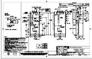
Figure 3–5: TYPICAL WIRING DIAGRAM FOR <strong>MIB</strong> RELAY<br />
3.2.4 TYPICAL WIRING DIAGRAM<br />
3-6 <strong>MIB</strong> <strong>High</strong> <strong>Impedance</strong> <strong>Bus</strong> <strong>Differential</strong> <strong>Relay</strong> <strong>GE</strong>K-106426D
3 HARDWARE 3.2 HIGH IMPEDANCE MODULE DESCRIPTION<br />
3.2.5 CONTROL POWER<br />
CAUTION: CONTROL POWER SUPPLIED TO THE RELAY MUST MATCH THE RATED VOLTA<strong>GE</strong> OF THE RELAY. IF<br />
THE VOLTA<strong>GE</strong> IS APPLIED TO THE WRONG TERMINALS, DAMA<strong>GE</strong> MAY OCCUR.<br />
Table 3–1: CONTROL POWER VOLTA<strong>GE</strong> RAN<strong>GE</strong><br />
RAN<strong>GE</strong> OPERATION RAN<strong>GE</strong><br />
LO 38.4-57.6 Vdc<br />
HI 100-150 Vdc<br />
<strong>GE</strong>K-106426D <strong>MIB</strong> <strong>High</strong> <strong>Impedance</strong> <strong>Bus</strong> <strong>Differential</strong> <strong>Relay</strong> 3-7<br />
3
3.2 HIGH IMPEDANCE MODULE DESCRIPTION 3 HARDWARE<br />
3.2.6 AC CURRENT TRANSFORMER INPUTS<br />
<strong>MIB</strong> current inputs are composed of four elements:<br />
1. Stabilizing resistor (inside HID).<br />
2. Varistor (inside HID)<br />
3. Contact from latching relay (inside HID)<br />
4. Current input in the high-speed overcurrent module.<br />
Depending on selected <strong>MIB</strong> model, the inputs configuration of <strong>High</strong> <strong>Impedance</strong> Device may change. If the Number of <strong>High</strong><br />
<strong>Impedance</strong> <strong>Differential</strong> Elements is 1, the HID will have only one input, If the Number of <strong>High</strong> <strong>Impedance</strong> <strong>Differential</strong><br />
Elements is 2, the HID will have two inputs, and If it is <strong>Bus</strong> / machine application it will have three inputs.<br />
Figure 3–6: <strong>MIB</strong> CURRENT INPUTS<br />
Current flows through stabilizing resistor into current input of the overcurrent module. Once high-speed overcurrent module<br />
trips, latching relay contacts short-circuit stabilizing resistor plus current input. In this way, excessive heating causing<br />
damage to resistors is avoided. MOV is used to avoid overvoltages damaging current input, limiting voltage to 1900V.<br />
3-8 <strong>MIB</strong> <strong>High</strong> <strong>Impedance</strong> <strong>Bus</strong> <strong>Differential</strong> <strong>Relay</strong> <strong>GE</strong>K-106426D
3 HARDWARE 3.3 HIGH-SPEED OVERCURRENT PROTECTION MODULE<br />
3.3HIGH-SPEED OVERCURRENT PROTECTION MODULE 3.3.1 MECHANICAL DESCRIPTION<br />
The high-speed overcurrent module is available in a box of a quarter of 19” rack four units high. The metallic case of the<br />
unit is highly resistant to corrosion. It is made of stainless steel (AISI 304), coated with an epoxy layer, and the rest of the<br />
metallic pieces are covered with a high quality resistive coating that has successfully passed at least 96 hours in the salt<br />
spray chamber (S/N ASTM B-117).<br />
The front of the relay is made of a shielded high quality thermoplastic, flame retardant (V0), highly resistive material, which<br />
guarantees the unit’s immunity to all types of EMI/RFI/ESD interference. As well, an IP52 (IEC 529) protection degree<br />
against dust and water through the front and with the relay mounted in the panel.<br />
The modular design of the relay simplifies repair or replacement of its components, without the need to manipulate the<br />
wiring. These types of operations must be performed exclusively by qualified personnel and only after removing auxiliary<br />
voltage from the unit.<br />
3.3.2 MOUNTING<br />
The high-speed overcurrent module is secured to the panel with the 4 M6 screws provided with the unit. This allows the<br />
user access to the front keypad, display and communication port. The wiring is at the rear of the unit. The drilling<br />
dimensions are shown on the drilling dimension diagram.<br />
Figure 3–7: HIGH-SPEED OVERCURRENT PROTECTION MODULE MOUNTING DIAGRAM<br />
3.3.3 REAR DESCRIPTION<br />
The module is wired through the terminal blocks located at the rear of the unit. In these terminal blocks, current terminals<br />
are shorted two-by-two when the module is extracted, so that the CT secondary never remains open. The maximum<br />
recommended cable section for this terminal board, with the appropriate terminal, is 6 mm2 (AWG 10).<br />
<strong>GE</strong>K-106426D <strong>MIB</strong> <strong>High</strong> <strong>Impedance</strong> <strong>Bus</strong> <strong>Differential</strong> <strong>Relay</strong> 3-9<br />
3
3.3 HIGH-SPEED OVERCURRENT PROTECTION MODULE 3 HARDWARE<br />
3.3.4 CONTACT INPUTS / OUTPUTS<br />
<strong>High</strong>-speed overcurrent modules have two contact inputs named CC1 and CC2. Default configuration for both inputs is:<br />
• CC1: 86a contact<br />
• CC2: All functions disable<br />
CC1 is intended to be used with an auxiliary contact from the latching relay (A7-A8) is shown in external wiring diagram). In<br />
this way, high-speed overcurrent module is able to know the latching relay status.<br />
Figure 3–8: CONTACT INPUTS CONNECTIONS<br />
Wet contacts must be connected to the inputs of the relay. A wet contact has one side connected to the positive terminal of<br />
an external DC power supply. The other side of this contact is connected to the required contact input terminal (A8 or A9).<br />
In addition, the negative side of the external source must be connected to the relay common (negative) terminal (A10). The<br />
maximum external voltage source voltage for this arrangement is 300 Vdc for HI models and 57.6 for LO models.<br />
The voltage threshold at which an input will detect a closed contact input depends on the relay model. For low voltage<br />
range relays (LO model), the threshold is set to 12 Vdc. For high voltage range relays (HI model), the voltage threshold is<br />
75 Vdc.<br />
In case of using AC voltage, it must be ensured that there is no voltage (less than 10 Vac) between the input common<br />
terminal, A10, and the ground terminal. The AC system must be line/neutral type, and not line/line, ensuring that the neutral<br />
and ground do not differ in more than 10 Vac. The reason for this is that there might be enough current circulating through<br />
the EMC filtering capacitors on these inputs to cause undesired activation.<br />
If it is not possible to ensure the previous conditions, the connection shown below can be used, where lines are wired only<br />
to inputs (A8 and A9), and the common (A10) is connected to the unit ground terminal.<br />
Figure 3–9: CONTACT INPUTS CONNECTIONS (AC ACTIVATION)<br />
3-10 <strong>MIB</strong> <strong>High</strong> <strong>Impedance</strong> <strong>Bus</strong> <strong>Differential</strong> <strong>Relay</strong> <strong>GE</strong>K-106426D
3 HARDWARE 3.3 HIGH-SPEED OVERCURRENT PROTECTION MODULE<br />
3.3.5 OUTPUT CONTACTS CONFIGURATION<br />
<strong>MIB</strong> relays provide one trip contact, one alarm (system ready) contact and four auxiliary contacts sharing one common<br />
located in the high-speed overcurrent module. All output relays are form C relays.All output relays are form C relays. Only<br />
one of the two states of the form C relay is connected to the output terminal. For each output relay it is possible to select<br />
which state is preferred to have at the MIFII terminals, NC (normally closed) or NO (normally open).<br />
Next figure shows the PCB of a relay, and the location of the jumpers used to select the configuration of each output<br />
contact (NO or NC).<br />
Figure 3–10: PCB SCHEME SHOWING THE JUMPERS TO CONFIGURE THE OUTPUT CONTACTS (NC / NO)<br />
<strong>GE</strong>K-106426D <strong>MIB</strong> <strong>High</strong> <strong>Impedance</strong> <strong>Bus</strong> <strong>Differential</strong> <strong>Relay</strong> 3-11<br />
3
3.3 HIGH-SPEED OVERCURRENT PROTECTION MODULE 3 HARDWARE<br />
3.3.6 OUTPUTS ISOLATION<br />
MII relays provide one trip contact, one alarm contact and four configurable contacts (option 1 and 2) sharing one common.<br />
An internal jumper, called Jx jumper, has been provided to allow splitting the four configurable outputs into two isolated<br />
groups. In this case, the number of outputs is reduced to three.<br />
Jx jumper is closed in the factory default configuration. (It is possible to order relays with Jx removed).<br />
The figure shows the factory default configuration with Jx Jumper closed. It is located on the soldering part of the PCB<br />
containing the inputs and outputs.<br />
Figure 3–11: JX JUMPER<br />
The Jx jumper is a tin-solder jumper easy to remove using a de-soldering tool.<br />
The standard factory default output contact configuration consists of one group of four outputs, with the same common. The<br />
figure below shows the configuration:<br />
3-12 <strong>MIB</strong> <strong>High</strong> <strong>Impedance</strong> <strong>Bus</strong> <strong>Differential</strong> <strong>Relay</strong> <strong>GE</strong>K-106426D
3 HARDWARE 3.3 HIGH-SPEED OVERCURRENT PROTECTION MODULE<br />
Each output has a different configuration, and it is able to operate independently to the others.<br />
If Jx jumper is removed, the output contact configuration change as shown in the following figure:<br />
After removing the Jx Jumper, the outputs are divided in two groups: Independent and isolated.<br />
Group1: Terminals B8-B7: Provide one output contact combining OUT1 and OUT2<br />
Group 2: Terminals B9-A7: OUT3 Standard output contact<br />
Terminals B10-A7: OUT4 Standard output contact<br />
3.3.6.1 OUTPUT CONFIGURATION AT TERMINALS B8-B7:<br />
To have a normally open contact across terminals B7-B8, configure OUT1 and OUT2 as shown bellow:<br />
• Remove JX internal jumper<br />
• Keep OUT1 and OUT2 as normally open contacts (factory default conf.)<br />
• Using the PC software, configure the two outputs to operate using the same internal signal. The internal signal used in<br />
the example is "XX TRIP"<br />
OUT1 and OUT2 must operate together to operate like a single output.The configuration of OUT1 and OUT2 must be the<br />
same so both outputs close.<br />
<strong>GE</strong>K-106426D <strong>MIB</strong> <strong>High</strong> <strong>Impedance</strong> <strong>Bus</strong> <strong>Differential</strong> <strong>Relay</strong> 3-13<br />
3
3.3 HIGH-SPEED OVERCURRENT PROTECTION MODULE 3 HARDWARE<br />
Figure 3–12: OUT1 AND OUT2 CONFIGURATION TO ACT AS A NORMALLY OPEN CONTACT<br />
3-14 <strong>MIB</strong> <strong>High</strong> <strong>Impedance</strong> <strong>Bus</strong> <strong>Differential</strong> <strong>Relay</strong> <strong>GE</strong>K-106426D
3 HARDWARE 3.3 HIGH-SPEED OVERCURRENT PROTECTION MODULE<br />
3.3.7 RS232 FRONT COMMUNICATIONS PORT<br />
A 9-pin RS232C serial port is located on the front of the relay for programming with a portable (personal) computer. All that<br />
is required to use this interface is a personal computer running the EnerVista MII SETUP software. Next figure shows the<br />
communications cable configuration.<br />
Figure 3–13: RS232 FRONT PORT CONNECTION<br />
WARNING: IN ORDER TO PREVENT DAMA<strong>GE</strong> BOTH TO THE PC SERIAL COMMUNICATIONS PORT AND THE<br />
RELAY FRONT RS232 PORT, IT IS COMPULSORY TO CONNECT THE RELAY GROUND TO THE SAME GROUND AS<br />
THE PC. OTHERWISE, USE AN UNGROUNDED COMPUTER.<br />
FOR THIS PURPOSE, PLEASE FOLLOW THE SAFETY INSTRUCTIONS IN CHAPTER 1<br />
<strong>GE</strong>K-106426D <strong>MIB</strong> <strong>High</strong> <strong>Impedance</strong> <strong>Bus</strong> <strong>Differential</strong> <strong>Relay</strong> 3-15<br />
3
3.3 HIGH-SPEED OVERCURRENT PROTECTION MODULE 3 HARDWARE<br />
3.3.8 RS485 COMMUNICATIONS PORT<br />
In addition to the front RS232 port, the relay provides the user with an additional RS485 communication port. RS485 data<br />
transmission and reception are accomplished over a single twisted pair that transmit and receive data alternating over the<br />
same two wires. Through the use of these port, continuous monitoring and control from a remote computer, SCADA system<br />
or PLC is possible.<br />
To minimize errors from noise, the use of shielded twisted pair wire is recommended. For a correct operation, polarity must<br />
be respected, although if it is not, there is no danger to damage the unit. For instance, the relays must be connected with all<br />
RS485 SDA terminals connected together, and all SDB terminals connected together. The RS485 standard refers only to<br />
terminals named “A” and “B”, although many devices use terminals named “+” and “-“. As a general rule, terminals “A”<br />
should be connected to terminals “-“, and terminals “B” to “+”. There are exceptions to this rule, such as the <strong>GE</strong> ALPS and<br />
DDS family of relays. The GND terminal should be connected to the common wire inside the shield, when provided.<br />
Otherwise, it should be connected to the shield. To avoid loop currents, the shield should be grounded at one point only.<br />
Each relay should also be daisy chained to the next one in the link. A maximum of 32 relays can be connected in this<br />
manner without exceeding driver capability. For larger systems, additional serial channels must be added. It is also possible<br />
to use commercially available repeaters to increase the number of relays on a single channel to more than 32. Do not use<br />
other connection configurations different than the recommended.<br />
Lightning strikes and ground surge currents can cause large momentary voltage differences between remote ends of the<br />
communication link. For this reason, surge protection devices are provided internally. To ensure maximum reliability, all<br />
equipment should have similar transient protection devices installed.<br />
Figure 3–14: RS485 SERIAL CONNECTION (B6366H5)<br />
3-16 <strong>MIB</strong> <strong>High</strong> <strong>Impedance</strong> <strong>Bus</strong> <strong>Differential</strong> <strong>Relay</strong> <strong>GE</strong>K-106426D
4 COMMUNICATIONS 4.1 ENERVISTA MII SETUP SOFTWARE<br />
4 COMMUNICATIONS 4.1ENERVISTA MII SETUP SOFTWARE 4.1.1 OVERVIEW<br />
IMPORTANT NOTE: MII FAMILY RELAYS CAN BE USED ONLY WITH ENERVISTA MII SETUP SOFTWARE.<br />
The EnerVista MII SETUP software package uses only Mod<strong>Bus</strong> protocols, and is designed to communicate with a single<br />
relay at a time. <strong>GE</strong> Multilin offers different communication software packages, such as <strong>GE</strong>-POWER and ENERVISTA,<br />
which can be used to communicate simultaneously with several relays.<br />
EnerVista MII SETUP software provides an easy way to configure, monitor and manage all <strong>MIB</strong> features.<br />
a) Setting files<br />
EnerVista MII SETUP software provides two ways of working with setting files:<br />
1.In off-line mode, disconnected from the relay, creating or editing setting files for a future download to the relay.<br />
2.Modifying directly the relay settings while connected to the relay.<br />
b) Configuration<br />
The configuration of inputs, outputs and LEDs can be modified, and internal logics with the different relay elements can<br />
be created.<br />
c) All metering values used by the unit can be monitored, as well as the internal states, inputs and outputs status.<br />
d) Performing the different available operations.<br />
e) Firmware updates.<br />
f) Viewing the different records stored in the relay, as events, oscillography, etc.<br />
The simplified use of the EnerVista MII SETUP software is as follows:<br />
Open *.ajs (settings) file<br />
Save the settings<br />
Execute<br />
ENERVISTA MII SETUP<br />
Modify the settings of<br />
the relay<br />
Send the settings to<br />
the relay<br />
Connect to the relay<br />
<strong>GE</strong>K-106426D <strong>MIB</strong> <strong>High</strong> <strong>Impedance</strong> <strong>Bus</strong> <strong>Differential</strong> <strong>Relay</strong> 4-1<br />
4
4.1 ENERVISTA MII SETUP SOFTWARE 4 COMMUNICATIONS<br />
4.1.2 STARTING COMMUNICATION<br />
Before the physical connection to the relay, it is important that the user reviews the safety instructions detailed in section 1.<br />
This section explains the importance of connecting both relay ground terminal and computer to a good grounding.<br />
Otherwise, communication may not be possible, or the relay and/or the computer could be damaged.<br />
To work online, the relay communication parameters (e.g. baud rate, relay address and password) must match the<br />
parameters in the computer.<br />
The computer parameters can be modified, in the Communication – Computer menu. Refer to the appropriate section in<br />
this same chapter for more details.<br />
The main screen of EnerVista MII SETUP software includes the following components:<br />
• Title<br />
• Main menu bar<br />
• Main icon bar<br />
• Working area<br />
• Status bar<br />
Figure 4–1: ENERVISTA MII SETUP MAIN SCREEN<br />
4.1.3 MAIN SCREEN<br />
4-2 <strong>MIB</strong> <strong>High</strong> <strong>Impedance</strong> <strong>Bus</strong> <strong>Differential</strong> <strong>Relay</strong> <strong>GE</strong>K-106426D
4 COMMUNICATIONS 4.2 FILE<br />
4.2FILE 4.2.1 NEW<br />
From the File – New option, the user can create a new file that will contain all the protection unit settings, as well as the<br />
relay configuration (inputs, outputs, events, oscillography, etc.).<br />
When the option is selected, the following screen will be shown. The user must select here a specific relay model matching<br />
exactly the relay model to which the settings and configuration will later be downloaded. The mentioned settings and<br />
configuration are related to the default factory settings of the relay.<br />
Figure 4–2: MODEL SELECTION<br />
Once the relay model is selected, the software will load the relay structure and will enable the Setpoint, Actual,<br />
Communication, View and Help menus for configuration.<br />
4.2.2 OPEN<br />
Option that allows to open previously created setting files for their modification.<br />
Once the relay model is selected, the program will enable Setpoint, Actual, Communication, View and Help sub-menus.<br />
<strong>GE</strong>K-106426D <strong>MIB</strong> <strong>High</strong> <strong>Impedance</strong> <strong>Bus</strong> <strong>Differential</strong> <strong>Relay</strong> 4-3<br />
4
4.2 FILE 4 COMMUNICATIONS<br />
4.2.3 PROPERTIES<br />
From the File – Properties option, the program will show a screen including the relay model information, firmware version,<br />
etc., as shown on Figure 4–3:<br />
Figure 4–3: MODEL/VERSION<br />
4.2.4 <strong>GE</strong>T INFO FROM RELAY<br />
The File – Get info from relay option enables the user to save the relay settings in a file on the hard disk of the computer.<br />
This file can later be opened offline to review and modify settings, and send them again to the relay after the modifications.<br />
4.2.5 SEND INFO TO RELAY<br />
The File – Set info to relay option enables to send to the relay a settings file stored on the hard disk of the computer.<br />
4-4 <strong>MIB</strong> <strong>High</strong> <strong>Impedance</strong> <strong>Bus</strong> <strong>Differential</strong> <strong>Relay</strong> <strong>GE</strong>K-106426D
4 COMMUNICATIONS 4.2 FILE<br />
4.2.6 PRINT SETUP<br />
The File – Print Setup option enables the user to configure the print setup for the settings file as shown in Figure 4–4:<br />
Figure 4–4: PRINTER SETUP<br />
4.2.7 PRINT PREVIEW<br />
The File – Print Preview option displays a preview of the settings print-out. It is also provides a quick view of all the relay<br />
settings at a glance, without having to navigate through the different menu trees. From this screen it is also possible to<br />
configure the printer that will be used, or to directly print the document. Double clicking on the document with the left mouse<br />
button will enlarge the document view, and double clicking with the right button will reduce the size.<br />
The available actions in this screen are shown in Figure 4–5:<br />
Figure 4–5: PRINT PREVIEW CONTROLS<br />
<strong>GE</strong>K-106426D <strong>MIB</strong> <strong>High</strong> <strong>Impedance</strong> <strong>Bus</strong> <strong>Differential</strong> <strong>Relay</strong> 4-5<br />
4
4.2 FILE 4 COMMUNICATIONS<br />
The File – Print option prints the relay settings using Windows default (active) printer.<br />
The File – Close option exits the program. It does not prompt for confirmation or save the open file.<br />
4.2.8 PRINT<br />
4.2.9 CLOSE<br />
4-6 <strong>MIB</strong> <strong>High</strong> <strong>Impedance</strong> <strong>Bus</strong> <strong>Differential</strong> <strong>Relay</strong> <strong>GE</strong>K-106426D
4 COMMUNICATIONS 4.3 SETPOINT<br />
4.3SETPOINT<br />
Clicking on the Setpoint menu entry gives access to Settings, Configuration, Logic Configuration and Clock.<br />
4.3.1 SETTINGS<br />
The Settings sub-menu is the same for all MII family relays, and shows all relay settings divided in two groups: Main<br />
Settings and Advanced Settings. The first settings group has basic settings (main protection functions). The second<br />
settings group includes more advanced settings (double settings group, customized curves, etc.), needed only if more<br />
complex protection schemes are required<br />
The purpose of this division is to simplify the use of the relay for those users only requiring the basic functionality of the<br />
relay.<br />
Figure 4–6: SETTINGS MENU<br />
Once in the corresponding sub-menu, either Main Settings or Advanced Settings, the procedure to enter and modify any<br />
setting value is the same:<br />
Select the settings group (the function selected in the example is the51P function in a MIFII).<br />
Edit the setting double-clicking on the value (for example, enable).<br />
Modify the value of the setting (see Figure 4–8: to Figure 4–10:).<br />
Confirm/Accept the modified value.<br />
Store the settings in the relay (if working in Emulation mode, this option stores them on the corresponding file) with the<br />
Store button. If the OK button is pressed without having pressed Store (a window asking confirmation will appear), the<br />
settings of this group will be discarded.<br />
<strong>GE</strong>K-106426D <strong>MIB</strong> <strong>High</strong> <strong>Impedance</strong> <strong>Bus</strong> <strong>Differential</strong> <strong>Relay</strong> 4-7<br />
4
4.3 SETPOINT 4 COMMUNICATIONS<br />
Figure 4–7: FUNCTION MENU<br />
Primarily there are four different setting formats:<br />
Boolean/Logic Settings (only two choices). For Boolean settings, the two possible options are shown so as the<br />
user can select which one is the appropriate, clicking with the mouse on the option<br />
desired.<br />
Numerical Settings For Numerical settings, a number must be entered. The program shows the minimum<br />
and maximum value for each setting, and it will not accept any value out of the<br />
corresponding range.<br />
Settings with a set of options For set of options settings, a pop-up window is shown, containing all possible values.<br />
Select the appropriate one clicking on it.<br />
Text Setting A text box is shown.<br />
Figure 4–8: LOGIC SETTING. Figure 4–9: NUMERIC SETTING. Figure 4–10: SET OF OPTIONS.<br />
4-8 <strong>MIB</strong> <strong>High</strong> <strong>Impedance</strong> <strong>Bus</strong> <strong>Differential</strong> <strong>Relay</strong> <strong>GE</strong>K-106426D
4 COMMUNICATIONS 4.3 SETPOINT<br />
4.3.2 MAIN SETTINGS<br />
4.3.2.1 <strong>GE</strong>NERAL SETTINGS<br />
General settings describe and activate the electric system settings where the relay is going to operate. Some of these<br />
settings will be used with measure values presentation purposes; however, some of them are directly applied during the<br />
sampling and analogical-numerical conversion process (nominal frequency setting). Therefore, these settings need to be<br />
altered so they fit with the system settings.<br />
4.3.2.2 GROUP 1- GROUP 2 FUNCTION SETTINGS<br />
The M family relays provide two independent setting groups. Group 1 is available in the Main Settings group, while Group<br />
2 can be accessed in the Advanced Settings group. The setting groups can be selected by digital input, through a<br />
communications command or from the EnerVista MII SETUP, or simply selecting it with the relay keypad. The setting that<br />
shows the active group can be found in General Advanced Settings.<br />
4.3.3 ADVANCED SETTINGS<br />
4.3.3.1 ADVANCED <strong>GE</strong>NERAL SETTINGS<br />
Advanced General Settings enables configuration of the active setting group as well as the minimum time the trip contact<br />
will remain closed, to let the circuit breaker open the circuit so as the contact does not get burnt.<br />
4.3.3.2 OTHER ADVANCED SETTINGS<br />
Besides the Flex Curve values, the user may configure the mask of events that will generate an event report and the events<br />
that will generate an oscillography.<br />
<strong>GE</strong>K-106426D <strong>MIB</strong> <strong>High</strong> <strong>Impedance</strong> <strong>Bus</strong> <strong>Differential</strong> <strong>Relay</strong> 4-9<br />
4
4.3 SETPOINT 4 COMMUNICATIONS<br />
4.3.4 RELAY CONFIGURATION<br />
Setpoint – <strong>Relay</strong> Configuration shows a dialog box to configure digital inputs, contact outputs and front panel LEDs, as<br />
shown in Figure 4–11:<br />
Figure 4–11: RELAY CONFIGURATION SETTINGS<br />
Each input, output and LED can be assigned an individual function (status bit) or an OR of a group of functions. Functions<br />
can also be assigned to virtual inputs and outputs, in order to allow greater flexibility when creating complex logics.<br />
The meaning of the different columns is explained below:<br />
• INPUT/LED/OUTPUT: Designates the respective element<br />
• I/O configuration: the appearance and function of this column can be, depending on the state of the respective OR<br />
checkbox column:<br />
- OR checkbox is not checked: the element consists of a drop down list in which the user can select the function that<br />
will activate the output or LED, or that will be activated by the input<br />
- OR checkbox is checked: the element consists of a button that will activate a new window (see Figure 4–12:)<br />
where the user can choose a sum of several functions that will activate the output or LED, or be activated by the<br />
input. These functions are distributed in groups, and only functions in the same group can be chosen for the same<br />
OR gate.<br />
4-10 <strong>MIB</strong> <strong>High</strong> <strong>Impedance</strong> <strong>Bus</strong> <strong>Differential</strong> <strong>Relay</strong> <strong>GE</strong>K-106426D
4 COMMUNICATIONS 4.3 SETPOINT<br />
• OR: activates the OR button for the I/O configuration column (see previous point). The window that appears when the<br />
OR button is pressed can be seen in Figure 4–12:<br />
Figure 4–12: OR ASSIGNMENT<br />
• NOT: when NOT checkbox is enabled, the logic is inverted. The element (input, output, LED) will actuate when the<br />
conditions are NOT fulfilled.<br />
• NAME: the user can write an identifying label of up to 4 characters that will get stored to be displayed later on.<br />
• BLINK (only for LEDs): the selection of BLINK checkbox makes the LED blink (alternatively switch ON and OFF)<br />
instead of being fixed when it is activated.<br />
• MEMORY (only for outputs and LEDs): when MEMORY checkbox is enabled, the respective element will be latched. If<br />
the cause that generated the activation of the output or LED does no longer exist, the element will remain active until a<br />
RESET command is performed.<br />
<strong>GE</strong>K-106426D <strong>MIB</strong> <strong>High</strong> <strong>Impedance</strong> <strong>Bus</strong> <strong>Differential</strong> <strong>Relay</strong> 4-11<br />
4
4.3 SETPOINT 4 COMMUNICATIONS<br />
4.3.5 LOGIC CONFIGURATION<br />
MII family relays can execute simple logic schemes that can be programmed from EnerVista MII SETUP. This logic<br />
schemes can be found at Setpoint – Logic Configuration.<br />
When one of the logics is selected, a new window will appear where the user can assign up to 8 inputs to the logic circuit.<br />
Each of these inputs can be a single function or status, as well as a logical union of several statuses.<br />
Figure 4–13: LOGIC CONFIGURATION<br />
The way the logic works is illustrated in the diagram at the right of the logic window.<br />
First, depending on the gate, up to 2 or 3 signals (internal flags coming from the status of the relay or from another logic, or<br />
external input signals) can be chosen as sources of each AND gate. The way they are programmed is similar to the way I/<br />
Os are (refer to relay configuration). The device will not take into account entries that are after an empty one. This means<br />
that every entry after the first empty one will be ignored. For example, if L1 IN1 is programmed but L1 IN2 is left empty, the<br />
relay will not take into account L1 IN3 and will directly evaluate L1 IN4. In the same way, the relay will ignore AND2 if AND1<br />
is not programmed, and will ignore AND3 if AND1 or AND2 are not programmed.<br />
Then the results from the AND gates are added by an OR gate that will produce the result of the logic.<br />
It is possible to set the pickup and dropout times for output from the OR gate. Example: for picking time of 10s and a<br />
dropout time of 15s, if input of the OR gate changes to 1, this input has to remain for 10s before the result of the logic<br />
changes to 1. If result of the OR gate drops to 0, output will be 1 for 15s and after that time output will be 0.<br />
See Chapter 7 for more details on logic configuration.<br />
4-12 <strong>MIB</strong> <strong>High</strong> <strong>Impedance</strong> <strong>Bus</strong> <strong>Differential</strong> <strong>Relay</strong> <strong>GE</strong>K-106426D
4 COMMUNICATIONS 4.3 SETPOINT<br />
The change date/time option opens a window with two choices:<br />
• Sending the PC date and time to the unit, this is, synchronizing the PC and the unit.<br />
• Selecting a date and a time and sending it to the relay.<br />
Figure 4–14: CHAN<strong>GE</strong> DATE/TIME<br />
4.3.6 DATE /TIME<br />
Once the new date and time have been sent, the user can check in the status graph, or even in the relay itself, that the new<br />
date/time has been correctly entered.<br />
<strong>GE</strong>K-106426D <strong>MIB</strong> <strong>High</strong> <strong>Impedance</strong> <strong>Bus</strong> <strong>Differential</strong> <strong>Relay</strong> 4-13<br />
4
4.4 ACTUAL 4 COMMUNICATIONS<br />
4.4ACTUAL 4.4.1 ACTUAL VALUES<br />
Actual - Actual values menu displays the Status Window shown in Figure 4–15:. This window shows internal relay<br />
information, measures, function status as well as additional information. There is a vertical scroll bar to navigate up and<br />
down the table to reach the desired information:<br />
• <strong>Relay</strong> model number and firmware version.<br />
• <strong>Relay</strong> internal date and time.<br />
• Values of currents, voltages and powers (phase and ground).<br />
• Protection function status (pickup / trip for each function).<br />
• Active settings group number.<br />
• Contact inputs and outputs status, and LEDs status.<br />
• Information from the self-test functions of the device.<br />
Figure 4–15: STATUS WINDOW<br />
4-14 <strong>MIB</strong> <strong>High</strong> <strong>Impedance</strong> <strong>Bus</strong> <strong>Differential</strong> <strong>Relay</strong> <strong>GE</strong>K-106426D
4 COMMUNICATIONS 4.4 ACTUAL<br />
4.4.2 EVENT RECORDER<br />
Actual – Event Recorder option makes the last 24 relay events to be retrieved (up to 32 for MIFII) and displayed in the<br />
window appearing in Figure 4–16:. Each event record is labeled with date, time (with 1msec. resolution), the cause of the<br />
event (pickup, trip of a certain function, etc.), and a list of the status of all inputs, outputs and functions during the event.<br />
Additionally, the program also shows current and voltage values for all phases and ground, frequency and single line<br />
sequence voltage during the event.<br />
Figure 4–16: EVENTS WINDOW<br />
The retrieved events can be reviewed in this window or also saved to disk (to be opened with EnerVista MII SETUP<br />
program) or exported to CSV (Comma Separated Values) format. This is a standard text table format that can be opened<br />
with most commercially available database or spreadsheet programs such as MS Access or Excel.<br />
<strong>GE</strong>K-106426D <strong>MIB</strong> <strong>High</strong> <strong>Impedance</strong> <strong>Bus</strong> <strong>Differential</strong> <strong>Relay</strong> 4-15<br />
4
4.4 ACTUAL 4 COMMUNICATIONS<br />
4.4.3 WAVEFORM CAPTURE<br />
In the Actual - WAVEFORM CAPTURE option, the user can start the process to retrieve the Oscillography record stored in<br />
the relay. The program will request the path and filename where the file is to be stored, by means of the following form:<br />
Figure 4–17: OSCILLOGRAPHY RECORD<br />
This file can be viewed using <strong>GE</strong>_OSC software (the use of this software is described in manual <strong>GE</strong>K-105596).<br />
4-16 <strong>MIB</strong> <strong>High</strong> <strong>Impedance</strong> <strong>Bus</strong> <strong>Differential</strong> <strong>Relay</strong> <strong>GE</strong>K-106426D
4 COMMUNICATIONS 4.5 OPERATIONS<br />
4.5OPERATIONS<br />
From Operations menu the user can perform all possible operation commands.<br />
Figure 4–18: OPERATIONS MENU<br />
<strong>GE</strong>K-106426D <strong>MIB</strong> <strong>High</strong> <strong>Impedance</strong> <strong>Bus</strong> <strong>Differential</strong> <strong>Relay</strong> 4-17<br />
4
4.6 COMMUNICATION 4 COMMUNICATIONS<br />
4.6COMMUNICATION<br />
The COMMUNICATION menu provides configuration options to communicate with the relay, as well as to perform a<br />
Mod<strong>Bus</strong> communication troubleshooting, or to update the relay with a new firmware.<br />
After making any change, pressing Store button saves the changes without exiting the window. Pressing OK saves and<br />
exits and pressing Cancel exits without saving changes.<br />
4.6.1 COMPUTER<br />
In COMPUTER dialog the user can configure the necessary adjustments to communicate with the relay from a PC.<br />
Figure 4–19: COMMUNICATIONS DIALOG<br />
4-18 <strong>MIB</strong> <strong>High</strong> <strong>Impedance</strong> <strong>Bus</strong> <strong>Differential</strong> <strong>Relay</strong> <strong>GE</strong>K-106426D
4 COMMUNICATIONS 4.6 COMMUNICATION<br />
4.6.1.1 COMPUTER SETTINGS<br />
In COMPUTER SETTINGS box the user can configure computer communication settings, besides the connection (Control<br />
Type) and Startup Mode.<br />
Control Type defines the connection type that is going to be used:<br />
• No control type for serial connection (front RS232 or rear RS485),<br />
• Mod<strong>Bus</strong>/TCP for Ethernet connection (by means of a serial/TCP converter). When this option is chosen, the serial<br />
configuration data disappears and a new box appears at the right to configure the IP address, the port number and the<br />
unit id.<br />
Figure 4–20: MODBUS/TCP SETUP<br />
• MODEM CONNECTION for modem serial connection. The modem configuration options appear at the right when this<br />
option is chosen.<br />
Defaults button returns the values to the factory default ones.<br />
4.6.1.2 COMMUNICATION CONTROL<br />
In COMMUNICATIONS CONTROL box the user can view the communication status (communicating to a relay or not),<br />
connect to a relay when the right parameters are entered in the Computer Settings box (ON button), or disconnect from the<br />
relay when desired (OFF button).<br />
Once the connection is established, when the user accesses any Setpoint or Operations, or Actual – Event Recorder i menu<br />
entries for the first time, the program will ask the relay password. The following window will appear:<br />
Figure 4–21: COMMUNICATION CONTROL – COMMUNICATING<br />
i. i.e., the first time a writing operation is performed against the relay during the current communication<br />
<strong>GE</strong>K-106426D <strong>MIB</strong> <strong>High</strong> <strong>Impedance</strong> <strong>Bus</strong> <strong>Differential</strong> <strong>Relay</strong> 4-19<br />
4
4.6 COMMUNICATION 4 COMMUNICATIONS<br />
4.6.1.3 COMMUNICATION OPTIMIZATION<br />
COMMUNICATIONS OPTIMIZATION box allows the user to enter values to control device response to communication<br />
attempts. Changing these parameters can improve communication, although it is recommended not to make changes to<br />
the default values if it is not required.<br />
Figure 4–22: COMMUNICATION OPTIMIZATION<br />
4.6.1.4 PRINT SCREEN<br />
When the Print Screen button is pressed, a new window appears asking if the user wants to capture the entire screen or<br />
only the active window (the one with all the communication parameters). Yes means capturing the whole screen and No<br />
means capturing only the communications window.<br />
Then a new window appears allowing to view the captured screen, to save the captured file in BMP or JPG format, or to<br />
print it (the print dialog window will appear so as the user can select which printer to use and enter the appropriate printer<br />
settings).<br />
Figure 4–23: PRINT SCREEN<br />
4-20 <strong>MIB</strong> <strong>High</strong> <strong>Impedance</strong> <strong>Bus</strong> <strong>Differential</strong> <strong>Relay</strong> <strong>GE</strong>K-106426D
4 COMMUNICATIONS 4.6 COMMUNICATION<br />
4.6.2 TROUBLESHOOTING<br />
The TROUBLESHOOTING option is available only when the PC is communicating with a relay. It is intended to check the<br />
Mod<strong>Bus</strong> communication frames between the PC and the relay. In the upper part, the user can read any readable value from<br />
the relay (setpoints, actual values) by entering the desired hexadecimal addressi , the type of data to read (Setpoints, Actual<br />
Values), the number of registers (the length of each register is of 2 bytes) and the format of the data (integer, long, float...),<br />
checking the checkbox at the left to make the PC start polling that address or unchecking it to stop.<br />
In the lower part, data can be sent to writable addresses of the relay. The working is similar to reading but, to send the data,<br />
the user must press the SEND button.<br />
Figure 4–24: TROUBLESHOOTING<br />
Refer to preceding section to learn about Print Screen button.<br />
i.To check how to read memory map addresses from the relay refer to the corresponding section further in this chapter<br />
<strong>GE</strong>K-106426D <strong>MIB</strong> <strong>High</strong> <strong>Impedance</strong> <strong>Bus</strong> <strong>Differential</strong> <strong>Relay</strong> 4-21<br />
4
4.6 COMMUNICATION 4 COMMUNICATIONS<br />
4.6.3 UPGRADE FIRMWARE VERSION<br />
IMPORTANT WARNING: For upgrading the relay firmware to version 4.00 or later, it is mandatory that the<br />
ENERVISTA MII Setup version is 1.10 or higher. For firmware version 5.00 or later, the ENERVISTA MII Setup<br />
version must be 2.10 or later. Otherwise it may result in damage to the relay<br />
The UPGRADE FIRMWARE VERSION option is active only when there is no active communication with the relay. If the PC<br />
is communicating with the relay, the user must switch communication off in Communication > Computer menu to activate<br />
this option.<br />
When this option is selected, a window appears asking for the new firmware version file to be uploaded to the relay:<br />
Figure 4–25: FLASH UPDATE FILE<br />
After selecting the file that will be used to update the FLASH memory, the following screen will be displayed:<br />
Figure 4–26: RELAY IDENTIFICATION<br />
After introducing the Slave Address and <strong>Relay</strong> password, the following screen will be displayed, showing details of the old<br />
model and the new model:<br />
Figure 4–27: UPDATE FLASH DIFFERENCES<br />
If the update is to a model option with higher functionality (see OPTION 1, OPTION 2 and OPTION R in the model list), the<br />
program will request a password. This password can be obtained placing an order with <strong>GE</strong> Multilin. The following three<br />
parameters must be clearly indicated in the order:<br />
• Serial number of the unit.<br />
• Current model option (before memory update).<br />
• Desired model option (after memory update).<br />
4-22 <strong>MIB</strong> <strong>High</strong> <strong>Impedance</strong> <strong>Bus</strong> <strong>Differential</strong> <strong>Relay</strong> <strong>GE</strong>K-106426D
4 COMMUNICATIONS 4.6 COMMUNICATION<br />
In a case where more than one unit needs to be updated, all the serial numbers must be detailed, and a different password<br />
will be assigned for each unit.<br />
Figure 4–28: PASSWORD<br />
If the update does not require changes to the functionality of the relay, the program will not request a password.<br />
After completing the previous screen, and during the loading process, the following screen will be displayed, showing the<br />
update process status:<br />
Figure 4–29: UPDATE PROCESS<br />
During the update, the display and LEDs will blink until the total completion of the process. Then the following screen will<br />
appear:<br />
Figure 4–30: UPDATE COMPLETED<br />
<strong>GE</strong>K-106426D <strong>MIB</strong> <strong>High</strong> <strong>Impedance</strong> <strong>Bus</strong> <strong>Differential</strong> <strong>Relay</strong> 4-23<br />
4
4.6 COMMUNICATION 4 COMMUNICATIONS<br />
It will take a few seconds for the relay to restart after the completion of the update process. Therefore, before unplugging<br />
the relay, please make sure that the relay main screen shows the analog inputs values.<br />
IMPORTANT NOTICE:<br />
The MODBUS ® memory map may change for different firmware versions. As a result, the Flash memory update, when<br />
upgrading to a higher model (OPTION 1 or 2), may involve a MODBUS ® memory map change. This may result a critical<br />
issue when the relay is integrated in a system, and the user should take into account the modifications that will have to be<br />
performed in the programs that access the <strong>MIB</strong> relay memory maps.<br />
Additionally, when a Flash memory update is performed, the loading program will enter the default settings. This<br />
means that the user will need to adapt the settings to the real situation of the protected device. If the user wants to keep the<br />
same settings after the memory update, a copy of the settings should be stored in a file before starting the update process.<br />
4-24 <strong>MIB</strong> <strong>High</strong> <strong>Impedance</strong> <strong>Bus</strong> <strong>Differential</strong> <strong>Relay</strong> <strong>GE</strong>K-106426D
4 COMMUNICATIONS 4.7 VIEW<br />
4.7VIEW 4.7.1 TRACES<br />
TRACES option is only active when the PC is communicating with the relay. If the communication is not established, to<br />
activate this option the user must switch communication on in Communication > Computer menu.<br />
When TRACES are active, the Mod<strong>Bus</strong> communication traces will be displayed in the lower part of the screen, as shown in<br />
Figure 4–31:<br />
Figure 4–31: MODBUS TRACES<br />
<strong>GE</strong>K-106426D <strong>MIB</strong> <strong>High</strong> <strong>Impedance</strong> <strong>Bus</strong> <strong>Differential</strong> <strong>Relay</strong> 4-25<br />
4
4.7 VIEW 4 COMMUNICATIONS<br />
4.7.2 MODBUS MEMORY MAP<br />
MODBUS MEMORY MAP option is only active when the PC is communicating with the relay. If the communication is not<br />
established, to activate this option the user must switch communication on in Communication > Computer menu.<br />
With MODBUS MEMORY MAP option the user can extract the complete memory map from the relay and print or save it in<br />
CSV format (to be later opened with any database or spreadsheet program as MS Excel). It is recommended to use this<br />
feature as memory map changes with relay model and firmware version so this is the safest way of obtaining the<br />
appropriate memory map for every single relay.<br />
Figure 4–32: MODBUS MEMORY MAP<br />
4-26 <strong>MIB</strong> <strong>High</strong> <strong>Impedance</strong> <strong>Bus</strong> <strong>Differential</strong> <strong>Relay</strong> <strong>GE</strong>K-106426D
4 COMMUNICATIONS 4.7 VIEW<br />
4.7.3 LANGUA<strong>GE</strong>S<br />
LANGUA<strong>GE</strong>S option is only active when there is no active communication with the relay. If the PC is communicating with<br />
the relay, to activate this option the user must switch communication off in Communication – Computer menu.<br />
Figure 4–33: LANGUA<strong>GE</strong>S<br />
<strong>GE</strong>K-106426D <strong>MIB</strong> <strong>High</strong> <strong>Impedance</strong> <strong>Bus</strong> <strong>Differential</strong> <strong>Relay</strong> 4-27<br />
4
4.7 VIEW 4 COMMUNICATIONS<br />
4-28 <strong>MIB</strong> <strong>High</strong> <strong>Impedance</strong> <strong>Bus</strong> <strong>Differential</strong> <strong>Relay</strong> <strong>GE</strong>K-106426D
5 SETTINGS 5.1 SETTINGS STRUCTURE<br />
5 SETTINGS 5.1SETTINGS STRUCTURE<br />
All the settings of the <strong>MIB</strong> relay, together with the procedures to change their value, are described in this chapter. First of<br />
all, a complete list of settings is shown; including ranges, units, step and factory default value. Then, the settings requiring<br />
more detailed comments are individually explained. In the EnerVista MII SETUP program, the settings are grouped under<br />
the Setpoint menu, Setpoint sub-menu entry.<br />
The <strong>MIB</strong> relay provides two settings groups (group 2 is accessible in the ADVANCED SETTINGS group), stored in<br />
EEPROM memory (permanent memory). Using a setting or through a communications command, it is possible to select<br />
which group is active, and then used by the relay protection algorithms.<br />
Settings can be accessed and modified either using the relay faceplate keypad, or using a computer connected to the relay<br />
through any of the relay communications ports, and the EnerVista MII SETUP program. The use of the keypad to modify<br />
settings is described in Chapter 8. If the computer is used to handle the settings, the following steps must be considered:<br />
Make sure your communication cable matches the scheme shown in Figure 3–13:<br />
Connect the communications cable between the relay (or modem) and the computer serial port.<br />
Run the EnerVista MII SETUP program. The procedure to install and use the EnerVista MII SETUP program is described in<br />
section 1.2.2 and in section 4.<br />
Make sure that the communications parameters in the relay match the EnerVista MII SETUP configuration settings<br />
(Communication - Computer Menu). The communications parameters shown in the relay faceplate display, within the<br />
configuration menu are:<br />
Comm Password<br />
Comm Baud Rate<br />
Slave Address<br />
For instructions on how to check and modify EnerVista MII SETUP program communications parameters please refer to<br />
chapter 4.<br />
Check that the relay number and password in the <strong>MIB</strong> display match the numbers entered in the dialog window of the<br />
EnerVista MII SETUP, after clicking on <strong>Relay</strong> Connection.<br />
<strong>GE</strong>K-106426D <strong>MIB</strong> <strong>High</strong> <strong>Impedance</strong> <strong>Bus</strong> <strong>Differential</strong> <strong>Relay</strong> 5-1<br />
5
5.2 MAIN SETTINGS 5 SETTINGS<br />
5.2MAIN SETTINGS 5.2.1 PRODUCT SETUP<br />
5-2 <strong>MIB</strong> <strong>High</strong> <strong>Impedance</strong> <strong>Bus</strong> <strong>Differential</strong> <strong>Relay</strong> <strong>GE</strong>K-106426D
5 SETTINGS 5.3 ADVANCED SETTINGS<br />
5.3ADVANCED SETTINGS 5.3.1 (DIFFERENTIAL ELEMENT 87 1<br />
5.3.2 DIFFERENTIAL ELEMENT 87 2<br />
5.3.3 <strong>GE</strong>NERAL ADVANCED<br />
<strong>GE</strong>K-106426D <strong>MIB</strong> <strong>High</strong> <strong>Impedance</strong> <strong>Bus</strong> <strong>Differential</strong> <strong>Relay</strong> 5-3<br />
5
5.3 ADVANCED SETTINGS 5 SETTINGS<br />
5.3.4 DIFFERENTIAL ELEMENT 87 1 GROUP 2<br />
5.3.5 DIFFERENTIAL ELEMENT 87 2 GROUP 2<br />
5-4 <strong>MIB</strong> <strong>High</strong> <strong>Impedance</strong> <strong>Bus</strong> <strong>Differential</strong> <strong>Relay</strong> <strong>GE</strong>K-106426D
5 SETTINGS 5.3 ADVANCED SETTINGS<br />
5.3.6 EVENTS AND OSCILLOGRAPHY MASKS (ONLY ENERVISTA MII SETUP)<br />
Event masks have two possible settings, YES or NO. If an action (e.g. the trip of a protection function) is set as<br />
YES, when the trip takes place an event will be generated. If it is set as NO, no event will be generated.<br />
EVENT ENERVISTA MII SETUP DEFAULT RAN<strong>GE</strong> STEP<br />
Phase A 87 1 Pickup Phase A 87 1 Pickup YES Y/N NA<br />
Phase B 87 1 Pickup Phase B 87 1 Pickup YES Y/N NA<br />
Phase C 87 1 Pickup Phase C 87 1 Pickup YES Y/N NA<br />
87 1 Pickup 87 1 Pickup YES Y/N NA<br />
Phase A 87 2 Pickup Phase A 87 2 Pickup YES Y/N NA<br />
Phase B 87 2 Pickup Phase B 87 2 Pickup YES Y/N NA<br />
Phase C 87 2 Pickup Phase C 87 2 Pickup YES Y/N NA<br />
87 2 Pickup 87 2 Pickup YES Y/N NA<br />
General Pickup General Pickup YES Y/N NA<br />
Phase A 87 1 Trip Phase A 87 1 Trip YES Y/N NA<br />
Phase B 87 1 Trip Phase B 87 1 Trip YES Y/N NA<br />
Phase C 87 1 Trip Phase C 87 1 Trip YES Y/N NA<br />
87 1 Trip 87 1 Trip YES Y/N NA<br />
Phase A 87 2 Trip Phase A 87 2 Trip YES Y/N NA<br />
Phase B 87 2 Trip Phase B 87 2 Trip YES Y/N NA<br />
Phase C 87 2 Trip Phase C 87 2 Trip YES Y/N NA<br />
87 2 Trip 87 2 Trip YES Y/N NA<br />
General trip General trip YES Y/N NA<br />
87 1 Disable by input 87 1 Disable by input YES Y/N NA<br />
87 2 Disable by input 87 2 Disable by input YES Y/N NA<br />
General Trip enable/disable by digital input Trip disabled(by DI) YES Y/N NA<br />
Protection status: in service/out of service Protection status YES Y/N NA<br />
<strong>Digital</strong> output1 active/non active Output 1 YES Y/N NA<br />
<strong>Digital</strong> output 2 active/non active Output 2 YES Y/N NA<br />
<strong>Digital</strong> output 3 active/non active Output 3 YES Y/N NA<br />
<strong>Digital</strong> output 4 active/non active Output 4 YES Y/N NA<br />
<strong>Digital</strong> input 1 active/non active <strong>Digital</strong> input 1 YES Y/N NA<br />
<strong>Digital</strong> input 2 active/non active <strong>Digital</strong> input 2 YES Y/N NA<br />
Settings change disabled by digital input Sett. change disable YES Y/N NA<br />
Trip operation by digital input Trip operation by input YES Y/N NA<br />
Trip operation by command Trip operation by command YES Y/N NA<br />
Auxiliary digital output latch reset Reset latch aux YES Y/N NA<br />
Group 2 selection by digital input Settings group change YES Y/N NA<br />
Oscillo trigger by digital input Oscillo trigg by DI YES Y/N NA<br />
86 Status 86 Status YES Y/N NA<br />
Reset 86 Reset 86 YES Y/N NA<br />
Oscillography trigger by command Oscillo trigg by comm YES Y/N NA<br />
Settings change Settings change YES Y/N NA<br />
EEPROM Failure EEPROM Failure YES Y/N NA<br />
User settings/Factory settings User settings YES Y/N NA<br />
<strong>GE</strong>K-106426D <strong>MIB</strong> <strong>High</strong> <strong>Impedance</strong> <strong>Bus</strong> <strong>Differential</strong> <strong>Relay</strong> 5-5<br />
5
5.3 ADVANCED SETTINGS 5 SETTINGS<br />
5.3.7 OSCILLOGRAPHY MASKS<br />
OSCILLOGRAPHY MASK ENERVISTA MII SETUP DEFAULT RAN<strong>GE</strong> STEP<br />
Oscillography Trigger by<br />
communications<br />
Oscillo by communic. NO Y/N NA<br />
Oscillography Trigger by digital input Oscillo by digital input NO Y/N NA<br />
Oscillography Trigger by tripping Oscillo by tripping NO Y/N NA<br />
Oscillography Trigger by pickup Oscillo by pickup NO Y/N NA<br />
5-6 <strong>MIB</strong> <strong>High</strong> <strong>Impedance</strong> <strong>Bus</strong> <strong>Differential</strong> <strong>Relay</strong> <strong>GE</strong>K-106426D
5 SETTINGS 5.4 TIME SYNCHRONIZATION<br />
5.4TIME SYNCHRONIZATION<br />
<strong>MIB</strong> includes an internal clock to time tag events. This clock can be either synchronized with the computer clock or set<br />
manually using the EnerVista MII SETUP software program (see Setpoints – Clock). It can also be set to a given Date and<br />
Time using the faceplate keypad (DATE & TIME menu entry).<br />
<strong>GE</strong>K-106426D <strong>MIB</strong> <strong>High</strong> <strong>Impedance</strong> <strong>Bus</strong> <strong>Differential</strong> <strong>Relay</strong> 5-7<br />
5
5.4 TIME SYNCHRONIZATION 5 SETTINGS<br />
5-8 <strong>MIB</strong> <strong>High</strong> <strong>Impedance</strong> <strong>Bus</strong> <strong>Differential</strong> <strong>Relay</strong> <strong>GE</strong>K-106426D
6 I/0 CONFIGURATION 6.1 INPUT CONFIGURATION<br />
6 I/0 CONFIGURATION 6.1INPUT CONFIGURATION 6.1.1 DESCRIPTION OF INPUTS<br />
incorporates 2 digital inputs, which can be configured using the EnerVista MII SETUP software (Setpoint > <strong>Relay</strong><br />
Configuration). The default input configuration is as follows:<br />
All elements not defined as PULSE are LEVEL inputs.<br />
In LEVEL inputs, while the voltage level is enough to activate the input, the input performs the function stated in its<br />
configuration.<br />
PULSE inputs are different. In the configuration menu for each input there are several states already defined as Pulse<br />
inputs. When the input recognizes their activation, it performs the function stated in its configuration, independently from the<br />
time it remains activated. For the input to perform again the required function, it is required that the input voltage level is<br />
reset and reactivated.<br />
LEVEL<br />
Input<br />
configuration<br />
response<br />
PULSE<br />
Input<br />
configuration<br />
response<br />
CC1<br />
<strong>MIB</strong><br />
86 A<br />
CC 2 All functions disable<br />
Figure 6–1: INPUT RESPONSE FOR LEVEL AND PULSE OPTIONS<br />
The minimum operation time for a valid PULSE input is over 0.015 seconds.<br />
Input elements are divided into three tthree groups, besides the No definition one. Up to eight elements can be configured<br />
to be activated by the same input, providing that they are all in the same group. Elements belonging to different groups<br />
need to be assigned to different inputs.<br />
In order to configure an input with more than one element from the same group, we must first activate the OR button, click<br />
on the I/O CONFIGURATION option and select the desired group, then select the desired elements. For inverting an<br />
element, select the NOT button. Finally, click the OK button.<br />
<strong>GE</strong>K-106426D <strong>MIB</strong> <strong>High</strong> <strong>Impedance</strong> <strong>Bus</strong> <strong>Differential</strong> <strong>Relay</strong> 6-1<br />
6
6.1 INPUT CONFIGURATION 6 I/0 CONFIGURATION<br />
INPUT CONFIGURATION WITH MORE THAN ONE FUNCTION (OR). EXAMPLE<br />
As shown on the figure below, input 1 is assigned to an OR. Clicking on that OR checkbox, a second screen named "OR<br />
ASSIGNMENT" is displayed, where the user can select the group that contains the desired elements (in this example,<br />
"INHIBITIONS BY DIGITAL INPUT 1"). This group includes 8 elements, from which we can select the ones we want to<br />
operate in the input, and invert them by clicking on the NOT checkbox. In the example below, all functions have been<br />
assigned to the input, and all of them have been inverted. Finally, to validate the selected configuration, the user must click<br />
on the OK button both in the "OR ASSIGNMENT" and the "I/O CONFIGURATION" screens.<br />
Figure 6–2: INPUT CONFIGURATION WITH MORE THAN ONE FUNCTION (OR)<br />
6-2 <strong>MIB</strong> <strong>High</strong> <strong>Impedance</strong> <strong>Bus</strong> <strong>Differential</strong> <strong>Relay</strong> <strong>GE</strong>K-106426D
6 I/0 CONFIGURATION 6.1 INPUT CONFIGURATION<br />
SIMPLE ACTION INPUT CONFIGURATION (ONE ELEMENT ASSIGNMENT)<br />
To assign breaker status input 52A to a digital input, select Breaker 52a from the I/O configuration selection list. The OR<br />
checkbox must not be selected.<br />
The simplest way of programming an input is to assign it to a single element. For this purpose, the user must simply open<br />
the I/O configuration selection list of the desired input. Once opened, all possible configuration functions will be shown, and<br />
the user will then be able to select one of them.<br />
To invert the selected function, the user must click on the NOT checkbox, to the right of the functions menu.<br />
Figure 6–3: SIMPLE ACTION INPUT CONFIGURATION (ONE ELEMENT ASSIGNMENT)<br />
In the example above, Input 2 has been programmed as 52a, inverted.<br />
In case the user wants to program more than one function for each input, then an OR must be selected, as in the example<br />
regarding input configuration with more than one element (OR).<br />
<strong>GE</strong>K-106426D <strong>MIB</strong> <strong>High</strong> <strong>Impedance</strong> <strong>Bus</strong> <strong>Differential</strong> <strong>Relay</strong> 6-3<br />
6
6.1 INPUT CONFIGURATION 6 I/0 CONFIGURATION<br />
6.1.2 INPUT ELEMENTS<br />
The following table shows the list of elements that can be assigned to each input. The table is divided into groups<br />
GROUP ENERVISTA MII SETUP FUNCIONALITY<br />
MASK ED 1<br />
No Definition Input not assigned<br />
87 1 Disable by Input Disable the operation (trip) of the 87 1 function<br />
87 2 Disable by Input Disable the operation (trip) of the 87 1 function<br />
MASK ED 2<br />
INPUTS<br />
DI all functions disable Disable the operation (trip) of every function<br />
Trip Disable (by DI) Disable the operation of the trip contact<br />
86B Input ‘B’ type contact of the latching relay<br />
86A Input ‘A’ type contact of the latching relay<br />
Trip Contact Close (PULSE) Activates trip contact<br />
Group Change If the input is activated the active settings group will be group 2. If it is not activated, the<br />
active settings group will be the adjusted in General Advanced Settings<br />
Sett. Change disable Activated, it disables the possibility that settings and active group be changed: switching<br />
to group 2 will only be possible through digital input Group change<br />
Reset (PULSE) LEDs and latched auxiliary outputs reset<br />
Oscillo Trigger (PULSE) Start oscillography storage<br />
General Input Generic element that may be used in logic configuration.<br />
6-4 <strong>MIB</strong> <strong>High</strong> <strong>Impedance</strong> <strong>Bus</strong> <strong>Differential</strong> <strong>Relay</strong> <strong>GE</strong>K-106426D
6 I/0 CONFIGURATION 6.2 OUTPUTS AND LEDS CONFIGURATION<br />
6.2OUTPUTS AND LEDS CONFIGURATION 6.2.1 DESCRIPTION OF OUTPUTS AND LEDS<br />
<strong>MIB</strong> incorporates 6 outputs and 6 LED indicators. 4 of the outputs and LED indicators are user configurable, and can only<br />
be programmed using EnerVista MII SETUP software (SETPOINT – RELAY CONFIGURATION). The first two LEDs are<br />
fixed for READY (System ready) and TRIP. The fixed outputs are programmed for ALARM (System alarm) and TRIP.<br />
The TRIP LED activates when the TRIP contact closes.<br />
The READY LED turns on when all the following conditions are fulfilled:<br />
• The relay status is READY<br />
• At least one of the protection functions of the active table is enabled<br />
• The trip of at least one of the enabled functions is also enabled.<br />
The default configuration for outputs is as follows:<br />
OUTPUT CONFIGURATION MEMORY<br />
1 87 1 Trip No<br />
2 87 2 Trip No<br />
3 Reset 86 No<br />
4 Trip No<br />
The default LED configuration is as follows:<br />
LED CONFIGURATION MEMORY<br />
3000 1000 & 2000<br />
1 Phase A Trip 87 1 Trip Yes<br />
2 Phase B Trip 87 2 Trip Yes<br />
3 Phase C Trip 87 1 Pickup Yes<br />
4 General Pickup 87 2 Pickup No<br />
<strong>GE</strong>K-106426D <strong>MIB</strong> <strong>High</strong> <strong>Impedance</strong> <strong>Bus</strong> <strong>Differential</strong> <strong>Relay</strong> 6-5<br />
6
6.2 OUTPUTS AND LEDS CONFIGURATION 6 I/0 CONFIGURATION<br />
Outputs/LEDs can be configured to be activated by a single element or by a sum of several of them. These elements are<br />
divided into eight groups, besides the No definition element. Elements belonging to the same group can be assigned to the<br />
same output/LED. Elements of different groups need to be assigned to different outputs/LEDs.<br />
In order to assign several elements to activate an output/LED, we first activate the OR button, next, click on the I/O<br />
CONFIGURATION frame and select the desired element group, then choose the desired elements. In order to invert an<br />
element, select the NOT button. Finally, click on the OK button.<br />
The Output/LED logic can inverted selecting the general NOT button. Outputs can be latched, and LEDs can be set to be<br />
fixed or blinking.<br />
Example:If we want to assign a phase A (<strong>High</strong> or low level) differential trip to an output or LED, the output or LED must be<br />
programmed with 87 1 function trip and 87 2 function trip. 50G1, 50G2 and DIS 51G1elements.To do this, check the OR<br />
box in the corresponding Output or LED line (for this case, Output1 and LED1). Then click on the OR button that appears in<br />
the I/O configuration column, select the desired group (TRIP1 and click the I/O configuration box for every element that will<br />
be blocked by the input.<br />
87 1 Trip<br />
87 2 Trip<br />
Local<br />
Elements from different groups cannot be included in an OR type logic.<br />
Output/LED<br />
OUTPUT/LED<br />
6-6 <strong>MIB</strong> <strong>High</strong> <strong>Impedance</strong> <strong>Bus</strong> <strong>Differential</strong> <strong>Relay</strong> <strong>GE</strong>K-106426D
6 I/0 CONFIGURATION 6.2 OUTPUTS AND LEDS CONFIGURATION<br />
6.2.2 OUTPUT AND LED ELEMENTS<br />
The list of elements that can be assigned to the different outputs and LEDs is divided into the following groups:<br />
Table 6–2: OUTPUTS AND LEDS ELEMENT<br />
GROUP FUNCTION DESCRIPTION<br />
NO DEFINITION OUTPUT OR LED NOT ASSIGNED<br />
87 1 A Trip Trip of phase A first level differential function<br />
87 1 B Trip Trip of phase B first level differential function<br />
87 1 C Trip Trip of phase C first level differential function<br />
TRIP 1<br />
87 1 Trip<br />
87 2 A Trip<br />
Trip of first level differential function (any phase)<br />
Trip of phase A second level differential function<br />
87 2 B Trip Trip of phase B second level differential function<br />
87 2 C Trip Trip of phase C second level differential function<br />
87 2 Trip Trip of second level differential function (any phase)<br />
TRIP 2 General trip Trip of any of the above mentioned functions<br />
87 1 A Pickup Pickup of phase A first level differential function<br />
87 1 B Pickup Pickup of phase B first level differential function<br />
87 1 C Pickup Pickup of phase C first level differential function<br />
PICKUP 1<br />
87 1 Pickup<br />
87 2 A Pickup<br />
Pickup of first level differential function (any phase)<br />
Pickup of phase A second level differential function<br />
87 2 B Pickup Pickup of phase B second level differential function<br />
87 2 C Pickup Pickup of phase C second level differential function<br />
87 2 Pickup Pickup of second level differential function (any phase)<br />
PICKUP 2 General Pickup Pickup of any of the above mentioned functions<br />
87 1 A Virtual Trip Phase A first level differential function: there is a trip condition<br />
87 1 B Virtual Trip Phase B first level differential function: there is a trip condition<br />
87 1 C Virtual Trip Phase C first level differential function: there is a trip condition<br />
TRIP READY 1<br />
87 1 Virtual Trip<br />
87 2 A Virtual Trip<br />
First level differential function (any phase): there is a trip condition<br />
Phase A second level differential function: there is a trip condition<br />
87 2 B Virtual Trip Phase B second level differential function: there is a trip condition<br />
87 2 C Virtual Trip Phase C second level differential function: there is a trip condition<br />
87 2 Virtual Trip <strong>High</strong> second differential function (any phase): there is a trip condition<br />
TRIP READY 2 General Virtual Trip Virtual trip of any of the above mentioned functions<br />
INPUTS / OUTPUTS<br />
MIXED 1<br />
Input 1 <strong>Digital</strong> input 1<br />
Input 2 <strong>Digital</strong> input 2<br />
86 Status Status of latching relay 86 (1=closed, 0=open)<br />
EEPROM Failure Active when a failure is detected in EEPROM management<br />
User settings Active when the default settings are active, not active when the user settings are<br />
active<br />
LEDs<br />
Ready Active when the relay is READY and at least one function is enabled and has trip<br />
enabled<br />
MISCELLANEOUS 2 Close Breaker Active when the close breaker operation is performed<br />
MIXED 2<br />
ACTIVE GROUP Settings group 2 is active<br />
Local Active when the relay display is inside MAIN SETTINGS, ADVANCED<br />
SETTINGS or OPERATIONS menu<br />
Virtual trip signals are activated as soon as the protection unit trip conditions are present, independently from the enable<br />
setting. This signal can be used to activate LEDs or auxiliary outputs. If the user wants the protection unit to trip, then the<br />
trip enable setting must be activated. In this case, the relay will activate the trip contact.<br />
<strong>GE</strong>K-106426D <strong>MIB</strong> <strong>High</strong> <strong>Impedance</strong> <strong>Bus</strong> <strong>Differential</strong> <strong>Relay</strong> 6-7<br />
6
6.2 OUTPUTS AND LEDS CONFIGURATION 6 I/0 CONFIGURATION<br />
6-8 <strong>MIB</strong> <strong>High</strong> <strong>Impedance</strong> <strong>Bus</strong> <strong>Differential</strong> <strong>Relay</strong> <strong>GE</strong>K-106426D
7 KEYPAD AND DISPLAY 7.1 DESCRIPTION<br />
7 KEYPAD AND DISPLAY 7.1DESCRIPTION<br />
has five types of display messages: actual values, main settings, advanced settings, operations and date & time. Actual<br />
values are values that are measured by the relay, such as currents; digital values of the relay, and can be digital inputs,<br />
outputs status and others; or internal information as the firmware revision. Main settings and advanced settings comprise<br />
product setup, communications and protection elements adjustments. Operations are the available commands that can be<br />
performed in the relay.<br />
These types of messages are located within a menu structure that groups the information into categories. This chapter<br />
describes the way to navigate this menu structure and shows the complete structure so that the user can reach certain<br />
screens quickly.<br />
<strong>GE</strong>K-106426D <strong>MIB</strong> <strong>High</strong> <strong>Impedance</strong> <strong>Bus</strong> <strong>Differential</strong> <strong>Relay</strong> 7-1<br />
7
7.2 FACEPLATE KEYPAD 7 KEYPAD AND DISPLAY<br />
7.2FACEPLATE KEYPAD<br />
The faceplate keypad is made up of five keys, as shown in Figure 7–1:<br />
Figure 7–1: KEYPAD<br />
The main screen is the one that shows the three phase and neutral currents. If the relay is not showing the main screen,<br />
you can return to it from any other screen by pressing the Escape key as many times as necessary until exiting the menu<br />
structure.<br />
From the main screen, the Menu key enters the menu structure. From that point on, the user can navigate through the<br />
menu structure using Up and Down arrows to move horizontally, Enter to enter submenus and Escape to exit to the upper<br />
level.<br />
7-2 <strong>MIB</strong> <strong>High</strong> <strong>Impedance</strong> <strong>Bus</strong> <strong>Differential</strong> <strong>Relay</strong> <strong>GE</strong>K-106426D
7 KEYPAD AND DISPLAY 7.3 ALPHANUMERIC DISPLAY AND LEDS<br />
7.3ALPHANUMERIC DISPLAY AND LEDS 7.3.1 DISPLAY<br />
The faceplate display of the relay is a 16 column x 2-row characters alphanumeric LCD display. Messages in the display<br />
are shown in the English language.<br />
Figure 7–2: DISPLAY<br />
The display contrast can be modified simultaneously pressing Escape + arrow:<br />
• Escape + up arrow increases the contrast<br />
• Escape + down arrow decreases the contrast<br />
If the keypad is not in use during 15 minutes, the display turns automatically off and returns to the main screen. Pressing<br />
ESC/RESET key, the display is automatically turned on and it shows the main screen with phase and groundcurrents.<br />
Pressing any other key, corresponding screen in the menu structure is shown. As an example, pressing ENTER key the<br />
Thermal Capacity Used screen is shown, as pressing this key the display enters in One Key Operation menu.<br />
7.3.2 LEDS<br />
The faceplate of the relay has six LEDs that show the relay status, as well as pickup and trip status. LEDs are grouped in<br />
two columns and three rows, as shown in the following figure:<br />
Figure 7–3: LEDS<br />
The two LEDs in the first row (Ready and Trip) are not configurable. For<strong>MIB</strong> relays the other four LEDs are configurable by<br />
the user, using EnerVista MII SETUP program. See Chapter 4 for more information on how to configure LEDs.The color of<br />
the four LEDs in rows 2 and 3 can be changed between red and green in any relay model. The way to do this is to press<br />
simultaneously up and down arrow keys for more than 2 seconds. Then a new menu appears:<br />
<strong>GE</strong>K-106426D <strong>MIB</strong> <strong>High</strong> <strong>Impedance</strong> <strong>Bus</strong> <strong>Differential</strong> <strong>Relay</strong> 7-3<br />
7
7.3 ALPHANUMERIC DISPLAY AND LEDS 7 KEYPAD AND DISPLAY<br />
Press up or down arrow<br />
to select, Enter to confirm<br />
Press up or down arrow<br />
to select, Enter to confirm<br />
Press up or down arrow<br />
to select, Enter to confirm<br />
Press up or down arrow<br />
to select, Enter to confirm<br />
COLOR LEDs MENU<br />
LED1 GREEN<br />
(:RED –:GREEN)<br />
Enter<br />
7-4 <strong>MIB</strong> <strong>High</strong> <strong>Impedance</strong> <strong>Bus</strong> <strong>Differential</strong> <strong>Relay</strong> <strong>GE</strong>K-106426D<br />
<br />
COLOR LEDs MENU<br />
LED2 RED<br />
(:RED –:GREEN)<br />
Enter<br />
<br />
COLOR LEDs MENU<br />
LED3 GREEN<br />
(:RED –:GREEN)<br />
Enter<br />
<br />
COLOR LEDs MENU<br />
LED4 RED<br />
(:RED –:GREEN)<br />
Enter<br />
Main Screen Ia 0.0 Ib 0.0<br />
<br />
Ic 0.0 mA
7 KEYPAD AND DISPLAY 7.4 OPERATIONS<br />
7.4OPERATIONS 7.4.1 ONE KEY OPERATION AND LAST TRIP DATA<br />
From the main screen, pressing Enter key the display shows a one-key operation menu that presents measures, thermal<br />
image value and up to five latest trip element data with the element that has tripped,and the secondary current value (not<br />
affected by CT ratio), with the day, month and time of the trip.<br />
When a fault occurs, trip information is automatically shown in the display. Pressing ENTER key, main screen will be shown<br />
again. In order to perform a RESET operation, display must be in main screen showing phase and ground currents, in this<br />
situation, pressing ESC/RESET key for more than 3 seconds a RESET operation will be performed.<br />
1. Day - month<br />
Main screen Ia 0.0 Ib 0.0<br />
Ic 0.0 mA<br />
Enter<br />
<br />
Last Trip Unit<br />
Enter<br />
<br />
1 st LTU 03-03 1 11:23:02<br />
1 ---- - ----<br />
Enter<br />
<br />
2 nd LTU 28-02 05:41:30<br />
2 ---- - ----<br />
Enter<br />
<br />
3 rd LTU 01-01 00:00:00<br />
3 ---- - ----<br />
Enter<br />
<br />
4 th LTU 01-01 00:00:00<br />
4 ---- - ----<br />
Enter<br />
<br />
5 th LTU 01-01 00:00:00<br />
5 ---- - ----<br />
7.4.2 HMI PASSWORD<br />
The relay allows settings protection by password. This password is called HMI password and it is disabled by default<br />
(value 0). If you change this value to other than 0, the HMI password will be enabled and required to change settings.<br />
When the password is enabled, a value between 1 and 9999 is shown on the screen. This number is the password<br />
value shown in a coded format.<br />
<strong>GE</strong>K-106426D <strong>MIB</strong> <strong>High</strong> <strong>Impedance</strong> <strong>Bus</strong> <strong>Differential</strong> <strong>Relay</strong> 7-5<br />
7
7.4 OPERATIONS 7 KEYPAD AND DISPLAY<br />
When a setting is being changed, after pressing the Enter key to store the modified value the relay shows the following<br />
screen:<br />
Scroll up and down with the arrow keys until the screen shows the desired password; next, press enter for confirmation and<br />
the relay will accept and store the setting change. The setting password protection will then be disabled for 15 minutes<br />
after the last setting change is made to the relay, or until a reset operation (the same as to reset LEDs, pressing Esc for<br />
more than 3 seconds from the main screen) is performed.<br />
The password can be modified in the Main Settings > Product Setup > HMI password menu. The relay then asks for the<br />
current password. Once it has been entered, the relay asks for the new password. Here is an example of how to change<br />
from HMI password value 1 to 2:<br />
If you don’t know the programmed password please contact <strong>GE</strong> Multilin Technical Service and have the encoded password<br />
value shown in Main Settings > Product Setup > HMI handy.<br />
7-6 <strong>MIB</strong> <strong>High</strong> <strong>Impedance</strong> <strong>Bus</strong> <strong>Differential</strong> <strong>Relay</strong> <strong>GE</strong>K-106426D
7 KEYPAD AND DISPLAY 7.5 MENU TREE<br />
7.5MENU TREE<br />
MENU<br />
ENTER<br />
ESC<br />
ENTER<br />
ESC<br />
<strong>MIB</strong><br />
ACTUAL VALUES<br />
<strong>MIB</strong><br />
MAIN SETTINGS<br />
ENTER<br />
ESC<br />
Order Code <strong>MIB</strong>30HICE00000<br />
Firmware Rev. 3.00<br />
Date & Time 20-02-03<br />
Hour 11:46:24<br />
SERIAL NUMBER 20.345.589<br />
<strong>Relay</strong> Name <strong>MIB</strong><br />
Phase A Diff. Current 0.00<br />
Phase B Diff. Current 0.00<br />
Phase C Diff. Current 0.00<br />
Frequency 0.00<br />
Input 1 0<br />
Input 2 0<br />
Output 1 0<br />
Output 2 0<br />
Output 3 0<br />
Output 4 0<br />
86 Status 0<br />
MAIN SETTINGS<br />
PRODUCT SETUP<br />
<strong>Relay</strong> Operation READY-DISABLE<br />
Frecuency 50-60<br />
HMI Password 0-9999<br />
Comm Password 1-255<br />
Slave Address 1-255<br />
Comm Baud Rate 0.3-19200 Baud<br />
<strong>GE</strong>K-106426D <strong>MIB</strong> <strong>High</strong> <strong>Impedance</strong> <strong>Bus</strong> <strong>Differential</strong> <strong>Relay</strong> 7-7<br />
7
7.5 MENU TREE 7 KEYPAD AND DISPLAY<br />
MENU<br />
ENTER<br />
ESC<br />
<strong>MIB</strong><br />
MAIN SETTINGS<br />
ENTER<br />
ESC<br />
ENTER<br />
ESC<br />
MAIN SETTINGS<br />
87 1 Function<br />
MAIN SETTINGS<br />
87 2 Function<br />
87 1 Enable Yes-No<br />
87 1 Trip Enable Yes-No<br />
87 1 Pickup Level 0.005-0.4<br />
87 1 Time Delay 0-600<br />
87 2 Enable Yes-No<br />
87 2 Trip Enable Yes-No<br />
87 2 Pickup Level 0.005-0.4<br />
87 2 Time Delay 0-600<br />
7-8 <strong>MIB</strong> <strong>High</strong> <strong>Impedance</strong> <strong>Bus</strong> <strong>Differential</strong> <strong>Relay</strong> <strong>GE</strong>K-106426D
7 KEYPAD AND DISPLAY 7.5 MENU TREE<br />
MENU<br />
ENTER<br />
ESC<br />
<strong>MIB</strong><br />
ADVANCED SETTINGS<br />
ENTER<br />
ESC<br />
ENTER<br />
ESC<br />
ENTER<br />
ESC<br />
ADVANCED SETTINGS<br />
<strong>GE</strong>NERAL ADVANCED<br />
ENTER<br />
ESC<br />
<strong>GE</strong>NERAL ADVANCED<br />
ADVANCED SETTINGS<br />
87 1 Function Group 2<br />
ADVANCED SETTINGS<br />
87 2 Function Group 2<br />
Settings Group 1-2<br />
Trip Min Time 50-300<br />
87 1 Enable Yes-No<br />
87 1 Trip Enable Yes-No<br />
87 1 Pickup Level 0.005-0.4<br />
87 1 Time Delay 0-600<br />
87 2 Enable Yes-No<br />
87 2 Trip Enable Yes-No<br />
87 2 Pickup Level 0.005-0.4<br />
87 2 Time Delay 0-600<br />
<strong>GE</strong>K-106426D <strong>MIB</strong> <strong>High</strong> <strong>Impedance</strong> <strong>Bus</strong> <strong>Differential</strong> <strong>Relay</strong> 7-9<br />
7
7.5 MENU TREE 7 KEYPAD AND DISPLAY<br />
MENU<br />
ENTER<br />
ESC<br />
ENTER<br />
ESC<br />
<strong>MIB</strong><br />
OPERATIONS<br />
ENTER<br />
ESC<br />
ENTER<br />
ESC<br />
ENTER<br />
ESC<br />
ENTER<br />
ESC<br />
ENTER<br />
ESC<br />
OPERATIONS<br />
LEDS RESET<br />
OPERATIONS<br />
ACTIVATE TABLE 1<br />
OPERATIONS<br />
ACTIVATE TABLE 2<br />
OPERATIONS<br />
RESET 86<br />
OPERATIONS<br />
CLOSE 86<br />
<strong>MIB</strong><br />
CHAN<strong>GE</strong> DATE & TIME<br />
YEAR<br />
MONTH<br />
DAY<br />
HOUR<br />
MINUTE<br />
DATE & TIME<br />
LEDS RESET ENTER<br />
TO CONFIRM<br />
ACTIVATE TABLE 1<br />
ENTER TO CONFIRM<br />
ACTIVATE TABLE 2<br />
ENTER TO CONFIRM<br />
RESET 86<br />
ENTER TO CONFIRM<br />
CLOSE 86<br />
ENTER TO CONFIRM<br />
PRESS<br />
PASSWORD<br />
LEDS RESET IN<br />
PROCESS<br />
ACTIVATE TABLE 1<br />
IN PROCESS<br />
ACTIVATE TABLE 2<br />
IN PROCESS<br />
RESET 86<br />
IN PROCESS<br />
CLOSE 86<br />
IN PROCESS<br />
LEDS RESET<br />
OPERATION OK<br />
ACTIVATE TABLE 1<br />
OPERATION OK<br />
ACTIVATE TABLE 2<br />
OPERATION OK<br />
RESET 86<br />
OPERATION OK<br />
CLOSE 86<br />
OPERATION OK<br />
7-10 <strong>MIB</strong> <strong>High</strong> <strong>Impedance</strong> <strong>Bus</strong> <strong>Differential</strong> <strong>Relay</strong> <strong>GE</strong>K-106426D
8 RELAY COMMISSIONING 8.1 VISUAL INSPECTION<br />
8 RELAY COMMISSIONING 8.1VISUAL INSPECTION<br />
Unpack the relay and verify that no parts are broken and that the relay has not suffered any damage during transit. Verify<br />
that the model number indicated on the faceplate corresponds to the model ordered.<br />
<strong>GE</strong>K-106426D <strong>MIB</strong> <strong>High</strong> <strong>Impedance</strong> <strong>Bus</strong> <strong>Differential</strong> <strong>Relay</strong> 8-1<br />
8
8.2 COMMENTS ON THE TEST EQUIPMENT 8 RELAY COMMISSIONING<br />
8.2COMMENTS ON THE TEST EQUIPMENT<br />
All devices that work with alternating current are influenced by frequency. Since a non-sinusoidal waveform results from a<br />
fundamental frequency wave plus a series of harmonics of this fundamental wave, it can be concluded that devices working<br />
with alternating current (relays) are influenced by the applied waveform.<br />
In order to correctly test relays that operate under alternating current, it is fundamental to use a sinusoidal current and/or<br />
voltage wave. The purity of the sinusoidal wave (the lack of harmonics) cannot be expressed in a specific form for a given<br />
relay. Each relay that is provided with tuned circuits, R-L and R-C circuits or non-linear elements (such a inverse time<br />
overcurrent relays) will be affected by non-sinusoidal waveforms.<br />
These relays respond to the current waveform in a different way from most AC ampere-meters. If the power supply network<br />
that is used for the test contains a considerable amount of harmonics, the ampere-meter and relay responses will be<br />
different.<br />
The relays are calibrated by the manufacturer using a 50 or 60 Hz power supply network with minimum harmonic contents.<br />
When the reception or installation tests are carried out, a power supply network with a harmonic-free waveform must be<br />
used.<br />
Ampere-meters and stop-watches that are used for carrying out the test must be calibrated and their accuracy must be<br />
better than that of the relay. The power supply network used for the tests must remain stable, mainly at levels close to the<br />
test pick-up current, as well as for the time for which the relay operates according to the curve under test.<br />
It is important to stress that the test accuracy depends on the power supply network conditions as well as on the<br />
instruments used. Functional tests carried out under inappropriate power supply conditions or using inappropriate<br />
instruments can be used for ensuring that the relay works roughly correctly and, therefore, for verifying its characteristics in<br />
an approximate manner.<br />
Here follows a list of tests that can be used to check that the unit is fully operational. For a more limited test for the<br />
reception of units we recommend carrying out only the tests listed in sections 9.5, 9.8, 9.10, 9.11, 9.12, 9.13, 9.14, 9.15,<br />
9.16, 9.17, 9.18 and 9.19.<br />
For verifying insulation, independent groups will be created, and voltage will be applied as follows:<br />
2500 RMS volts will be applied progressively among all terminals in a group, short-circuited between them and the<br />
case, during one second.<br />
2500 RMS volts will be applied progressively between groups, during one second.<br />
The independent groups on the relay are as follows:<br />
NOTE:<br />
Group 1: A1, A2 Power Supply<br />
Group 2: C1 to C6 Current Transformers<br />
Group 3: A8, A9, A10 Contact Inputs<br />
Group 4: A5, A6 Trip<br />
Group 5: B7, B8, B9, B10, A7 Contact Outputs<br />
In case of performing this test on all terminals at the same time, have in mind that the consumption will increase,<br />
due to the impedance of the capacitors inside the relay, used to derive high frequency surges to ground. The<br />
consumption will be approximately, 3 mA at 2000 Volts for each input.<br />
In case the Hi-Pot device used to test the relay trips due to excessive consumption, apply the test between each<br />
group and ground one at a time.<br />
NOTE: Do not test insulation on terminals B12, A12 and B11 (RS485). These terminals must be grounded during<br />
the test.<br />
DURING TESTS, GND TERMINAL MUST BE<br />
GROUNDED FOR SAFETY REASONS<br />
8-2 <strong>MIB</strong> <strong>High</strong> <strong>Impedance</strong> <strong>Bus</strong> <strong>Differential</strong> <strong>Relay</strong> <strong>GE</strong>K-106426D
8 RELAY COMMISSIONING 8.3 RELAY SETTING<br />
8.3RELAY SETTING<br />
When the relay is shipped from our factory, it has default settings, which are the starting point for the following tests.<br />
An exhaustive list of all the settings necessary for each test will not be given here. Just the specific settings required for<br />
each test are indicated, and it can be supposed that the other settings do not affect the test being performed.<br />
We must take into account that these tests are only valid for the default factory configuration. Different configurations<br />
involving modifications in certain elements, such as different contact configuration, will require a subsequent modification of<br />
the test procedure.<br />
Acceptance tests are explained assuming the default settings.<br />
<strong>GE</strong>K-106426D <strong>MIB</strong> <strong>High</strong> <strong>Impedance</strong> <strong>Bus</strong> <strong>Differential</strong> <strong>Relay</strong> 8-3<br />
8
8.4 WIRING AND NECESSARY EQUIPMENT 8 RELAY COMMISSIONING<br />
8.4WIRING AND NECESSARY EQUIPMENT<br />
Necessary equipment:<br />
• 1 AC current source .<br />
• 1 DC voltage power supply.<br />
• 1 timing device.<br />
• 1 Multi-meter.<br />
• Optionally, it is advisable to have a PC available, with the EnerVista MII SETUP software installed.<br />
• <strong>Relay</strong> wiring diagram.<br />
Connect the relay as shown in<br />
For safety reasons, the external protection earth terminal should be securely grounded.<br />
Supply the unit through terminals A1 and A2 at the rated voltage<br />
.<br />
<strong>MIB</strong><br />
Overcurrent<br />
Module<br />
A1<br />
A2<br />
A5<br />
A6<br />
Phase Overcurrent<br />
Module<br />
X Y<br />
A C1 C2<br />
B C3 C4<br />
C C5 C6<br />
NOTE: Terminals for current injection<br />
Figure 8–1: TEST CONNECTIONS FOR <strong>MIB</strong> (RELAY<br />
8-4 <strong>MIB</strong> <strong>High</strong> <strong>Impedance</strong> <strong>Bus</strong> <strong>Differential</strong> <strong>Relay</strong> <strong>GE</strong>K-106426D<br />
Iac
8 RELAY COMMISSIONING 8.5 TAR<strong>GE</strong>T LEDS<br />
8.5TAR<strong>GE</strong>T LEDS<br />
Check that pressing the “ESC/RESET” button for more than 3 seconds, all the front target LEDs light up and reset.<br />
<strong>GE</strong>K-106426D <strong>MIB</strong> <strong>High</strong> <strong>Impedance</strong> <strong>Bus</strong> <strong>Differential</strong> <strong>Relay</strong> 8-5<br />
8
8.6 POWER SUPPLY TEST 8 RELAY COMMISSIONING<br />
8.6POWER SUPPLY TEST<br />
Connect the relay to a power supply at rated minimum voltageindicated in the table below<br />
A (C1-C2 terminals) a current equal to 0.1 amp.The . will trip and close trip contact and OUT1 and OUT4 outputs. Under<br />
these tripping conditions check that the READY(B5-B6 terminals) output is open, and trip contact (A5-A6 terminals) and<br />
OUT1 (A7-B7 terminals) and OUT4 (A7-B10 terminals) auxiliary contacts are closed. Also check that the relay can<br />
communicate with the PC program in case you are using the relay connected to a PC:<br />
Voltage test and maximum consumption is shown below:<br />
<strong>GE</strong>NERAL SETTINGS<br />
<strong>Relay</strong> Status RDY<br />
Frequency<br />
87 1 FUNCTION<br />
Line frequency<br />
87 1 Enable YES<br />
87 1 Trip Enable YES<br />
87 1 Pickup level 0.010 A<br />
87 1 Time Delay 1 sec<br />
Model “LO” (24 - 48 Vdc)<br />
Voltage (Vdc) Maximum Consumption (mA)<br />
18 900<br />
48 300<br />
58 250<br />
Model “HI” (110 - 250 Vdc 120-230 Vac)<br />
Voltage (Vdc) Maximum Consumption (mA)<br />
88 130<br />
110 105<br />
250 55<br />
Voltage (Vac) Maximum Consumption (mA)<br />
110 200<br />
220 140<br />
Shown values are only illustrative, as due to the nature of the internal power supply (switched power supply), the<br />
consumption currents are high frequency currents, and the meters used measure these values with a poor accuracy.<br />
8-6 <strong>MIB</strong> <strong>High</strong> <strong>Impedance</strong> <strong>Bus</strong> <strong>Differential</strong> <strong>Relay</strong> <strong>GE</strong>K-106426D
8 RELAY COMMISSIONING 8.7 COMMUNICATIONS<br />
8.7COMMUNICATIONS<br />
The communication test checks that the 2 communications ports (the front RS232 and the rear RS485) work properly. To<br />
perform this test is necessary to establish the connection between the PC and the relay (refer to figure 3-10). If the front<br />
port is used, a straight through cable is needed. If the rear RS485 port is used, an RS485/RS232 converter is needed. <strong>GE</strong><br />
Multilin offers DAC300, F485 or RS232/485 converters.<br />
The communications parameters that have to be set in the computer should match the relay default communication<br />
settings.<br />
The factory default settings for the <strong>MIB</strong> relay are:<br />
COMMUNICATIONS<br />
NAME VALUE UNITS RAN<strong>GE</strong><br />
Slave Address 1 1 - 255<br />
Communication Port COM1 COM1 – COM*<br />
Baud Rate 9.600 Bauds 300 – 19 200<br />
Parity NONE NONE – ODD - EVEN<br />
Control type No control type No control type, Modem<br />
connection, MODBUS/TCP<br />
Start up mode File Mode Communicate with relay –<br />
File mode<br />
Using the EnerVista MII SETUP program, communicate with the relay and in the Status window check that the<br />
communications are not lost at any time. Perform this test on both communications ports.<br />
This test is carried up at the minimum and maximum voltage that the relay allows (+-20 of the rated voltage)<br />
<strong>GE</strong>K-106426D <strong>MIB</strong> <strong>High</strong> <strong>Impedance</strong> <strong>Bus</strong> <strong>Differential</strong> <strong>Relay</strong> 8-7<br />
8
8.8 RELAY SETTING 8 RELAY COMMISSIONING<br />
8.8RELAY SETTING<br />
When the relay is shipped from the factory, it comes with a default set of settings, which act as the starting point for the<br />
following tests.<br />
Since the <strong>MIB</strong> relay has a large number of settings, a list of all the settings necessary for all tests will not be given here, but<br />
rather only the specific settings required for each test indicated.<br />
These tests are only valid for the default factory configuration. Different configurations involving modifications in certain<br />
elements, such as different contact configuration, will require a subsequent modification of the test procedure.<br />
8-8 <strong>MIB</strong> <strong>High</strong> <strong>Impedance</strong> <strong>Bus</strong> <strong>Differential</strong> <strong>Relay</strong> <strong>GE</strong>K-106426D
8 RELAY COMMISSIONING 8.9 CONTACT INPUTS<br />
8.9CONTACT INPUTS<br />
Sequentially apply the rated voltage to input CC1 and CC2 (A8-A10 and A9-A10).<br />
Check that when voltage is applied to one contact input, only this input gets active, and the other one remains inactive. Use<br />
the INFORMATION menu on the faceplate or a PC and the ACTUAL VALUES menu in the EnerVista MII SETUP program<br />
(Actual> Actual Values) to easily check which input gets active for each test.<br />
Repeat this test at minimum and maximum permissible voltages.<br />
<strong>GE</strong>K-106426D <strong>MIB</strong> <strong>High</strong> <strong>Impedance</strong> <strong>Bus</strong> <strong>Differential</strong> <strong>Relay</strong> 8-9<br />
8
8.10 CONTACT OUTPUTS 8 RELAY COMMISSIONING<br />
8.10CONTACT OUTPUTS<br />
Check that all the outputs are open.<br />
Set the relay as follows:<br />
87 2<br />
NAME VALUE UNITS RAN<strong>GE</strong><br />
87 2 Enable Yes Yes/No<br />
87 2 Trip Enable Yes Yes/No<br />
87 2 Pickup level 0.01 Amps 0.005 – 0.4<br />
87 2 Time Delay 0 Seconds 0 - 600<br />
Inject a current through phase A terminals equal to 0.1 amp to trip the relay. Check that the trip output (terminals A5-A6)<br />
and auxiliary output OUT2 (terminals A7-B8) and OUT4 (terminals A7-B10) close, and the PICKUP (LED4), and OP 87A<br />
(LED1) LEDs lights up.<br />
Inject a current through phase B terminals equal to 0.1 amp to trip the relay. Check that the trip output (terminals A5-A6)<br />
and auxiliary output OUT2 (terminals A7-B8) and OUT4 (terminals A7-B10) close, and the PICK UP (LED4), OP 87B<br />
(LED2) and TRIP LEDs light up.<br />
Inject a current through phase C terminals equal to 0.1 amp1 x In (phase) to trip the relay. Check that the trip output<br />
(terminals A5-A6) and auxiliary output OUT2 (terminals A7-B8) and OUT4 (terminals A7-B10) close, and the PICK UP<br />
(LED4), OP 87C (LED3) and TRIP LEDs light up.<br />
Remove the Power Supply from the relay and check that the READY contact (terminals B5-B6) closes. Power on the relay<br />
again and check that the READY (terminals B5-B6) contact opens.<br />
8-10 <strong>MIB</strong> <strong>High</strong> <strong>Impedance</strong> <strong>Bus</strong> <strong>Differential</strong> <strong>Relay</strong> <strong>GE</strong>K-106426D
8 RELAY COMMISSIONING 8.11 RELAY METERING<br />
8.11 RELAY METERING 8.11.1 CURRENT METERING<br />
Set the relay to the same frequency than the AC source used and apply the following currents:<br />
PHASE 1 2 3<br />
Ia (Amps) 0.2 amps (phase)<br />
Ib (Amps) 0.1 amps (phase) 0.3 amps (phase)<br />
Ic (Amps)<br />
Check that the relay measures Ia, Ib and Ic with an accuracy better than 5%<br />
<strong>GE</strong>K-106426D <strong>MIB</strong> <strong>High</strong> <strong>Impedance</strong> <strong>Bus</strong> <strong>Differential</strong> <strong>Relay</strong> 8-11<br />
8
8.12 DIFERENTIAL UNIT LEVEL 1 (F87 1) 8 RELAY COMMISSIONING<br />
8.12DIFERENTIAL UNIT LEVEL 1 (F87 1)<br />
Enable only 87 1 function.<br />
Set its time delay and pickup to 0.1 A.<br />
With 0.9 times the pickup current the relay should not trip.<br />
With 1.1 times the pickup current the relay should trip in between 10 to 50 ms.<br />
With 4 times the pickup current the relay should trip in less than 15 ms.<br />
The test should be carried out for phases A, B and C.<br />
8-12 <strong>MIB</strong> <strong>High</strong> <strong>Impedance</strong> <strong>Bus</strong> <strong>Differential</strong> <strong>Relay</strong> <strong>GE</strong>K-106426D
8 RELAY COMMISSIONING 8.13 DIFERENTIAL UNIT LEVEL 2 (F87 2)<br />
8.13DIFERENTIAL UNIT LEVEL 2 (F87 2)<br />
Enable only 87 2 function.<br />
Set its time delay and pickup to 0.1 A.<br />
With 0.9 times the pickup current the relay should not trip.<br />
With 1.1 times the pickup current the relay should trip in between 10 to 50 ms.<br />
With 4 times the pickup current the relay should trip in less than 15 ms.<br />
The test should be carried out for phases A, B and C.<br />
<strong>GE</strong>K-106426D <strong>MIB</strong> <strong>High</strong> <strong>Impedance</strong> <strong>Bus</strong> <strong>Differential</strong> <strong>Relay</strong> 8-13<br />
8
8.14 TIME SYNCHRONIZATION 8 RELAY COMMISSIONING<br />
8.14TIME SYNCHRONIZATION<br />
Synchronize the relay date and time with the PC, using the EnerVista MII SETUP communications program (SETPOINT –<br />
CLOCK). Check using the keypad and display that the relay is actually in synchronism with the computer.<br />
8-14 <strong>MIB</strong> <strong>High</strong> <strong>Impedance</strong> <strong>Bus</strong> <strong>Differential</strong> <strong>Relay</strong> <strong>GE</strong>K-106426D
8 RELAY COMMISSIONING 8.15 ACCEPTANCE TEST FOR HIGH IMPEDANCE MODULE<br />
8.15ACCEPTANCE TEST FOR HIGH IMPEDANCE MODULE 8.15.1 WIRING AND NECESSARY EQUIPMENT<br />
Necessary equipment:<br />
1 AC voltage source.<br />
1 DC voltage power supply.<br />
1 timer.<br />
1 Multi-meter.<br />
Typical wiring diagram: (3000) B5177F1<br />
(2000) B5177F2<br />
(1000) B5177F3<br />
Test equipment:<br />
A multimeter or continuity measurer with a maximum threshold of 110 Ω.<br />
Method:<br />
Check for continuity between the grounded screw and any metallic point of the case that has no painting on it.<br />
8.15.2 CONTINUITY<br />
8.15.3 ISOLATION TEST<br />
IMPORTANT:<br />
During all tests, the screw located on the rear of the relay must be grounded.<br />
For verifying isolation, independent groups will be created, and voltage will be applied as follows:<br />
2500 RMS volts will be applied progressively among all terminals in a group, short-circuited between them and the<br />
case, during one second. In case the Hi-Pot device used to test the relay trips due to excessive consumption, apply the<br />
test between each group and ground one at a time.<br />
2500 RMS volts will be applied progressively between groups, during one second.<br />
•Group 1 (LATCHING RELAY contacts): A5 – A6 – A7 – A8– A9 – A10– A11 – A12– B1 – B2– B3 – B4– B5 – B6 –<br />
B7 – B8<br />
•Group 2 (LATCHING RELAY coils): A1 – A4 – B9 – B12<br />
•Group 3 (Pushbutton)*: C5 – C6 – C7 – C8<br />
•Group 4 (Analogical Group): C10 – C11 – C12 – D6 – D7 – D8 – D2 – D3 – D4<br />
Consumption will not be higher than 20 mA.<br />
*NOTE:Use terminal C5 for 125 Vdc power supply. For power supply from 125 Vdc to 250 Vdc use C1 terminal.<br />
Latching relay Coil Resistor (HID module)<br />
POWER SUPPLY A1 – A3 TERMINALS B10 – B12 TERMINALS<br />
LO 340 OHM 340 OHM<br />
HI 2K15 2K15<br />
NOTE: Accuracy of 20%.<br />
8.15.4 MEASURES<br />
<strong>GE</strong>K-106426D <strong>MIB</strong> <strong>High</strong> <strong>Impedance</strong> <strong>Bus</strong> <strong>Differential</strong> <strong>Relay</strong> 8-15<br />
8
8.15 ACCEPTANCE TEST FOR HIGH IMPEDANCE MODULE 8 RELAY COMMISSIONING<br />
Resistors Measure<br />
Check that the resistor value between terminals is 2K:<br />
NOTE: Accuracy of 12%.<br />
C12 – D8<br />
C11 – D7<br />
C10 – D6<br />
Thyrites current measure:<br />
MOV TERMINALS APPLIED VOLTA<strong>GE</strong> 290 VCA<br />
UL NOT UL<br />
C12-D4 300 - 550 uA 2 - 10 mA<br />
C11-D3 (Only for HID 3<br />
and HID 2)<br />
300 - 550 uA 2-10 mA<br />
C10-D2 (Only for HID3) 300 - 550 uA 2 - 10 mA<br />
8.15.5 LATCHING RELAY<br />
Contact test:<br />
• Check with the external wiring diagram that all the auxiliary contacts of the latching relay are open and, therefore, there<br />
is no continuity between them.<br />
• Apply voltage to terminals +A1 y –A4 and verify that latching relay contacts operation time is below 25 ms.<br />
• Verify that all auxiliary contacts have changed their position to closed and that there is continuity between each pair of<br />
them.<br />
• Apply voltage to terminals +B9 and –B12 and verify that latching relay contacts opening time is below 20 ms.<br />
• Check that all auxiliary contacts have changed to their default position (open) and, therefore, there is no continuity<br />
between each pair of them<br />
Lamp:<br />
• By having the latching relay in the reset position, apply the latching relay rated voltage to terminals C6(+) and C9(-)<br />
and check that the button lightens up.<br />
• Switch the voltage off and check the lamp turns off.<br />
• Without any DC supply at C7-C8 terminals, check with a Resistance test that when pressing the button<br />
there is full continuity between C7 and C8 terminals.<br />
8-16 <strong>MIB</strong> <strong>High</strong> <strong>Impedance</strong> <strong>Bus</strong> <strong>Differential</strong> <strong>Relay</strong> <strong>GE</strong>K-106426D
8 RELAY COMMISSIONING 8.16 USER SETTINGS<br />
8.16USER SETTINGS<br />
The following pages intend to be useful to register the user settings. They can be used as a guide or template or to record<br />
the relay settings, in case your company does not provide a propietary form sheet.<br />
8.16.1 MAIN SETTINGS<br />
8.16.1.1 <strong>GE</strong>NERAL SETTINGS<br />
ENERVISTA MII SETUP HMI USER VALUE RAN<strong>GE</strong> STEP<br />
<strong>GE</strong>NERAL SETTINGS PRODUCT SETUP <strong>GE</strong>NERAL<br />
<strong>Relay</strong> Status <strong>Relay</strong> Operation STA RDY / DIS NA<br />
Frequency Frequency FRQ 50/60 Hz NA<br />
Password --- PWD 1 – 255<br />
Address --- ADD 1 – 255 1<br />
Communications Speed --- BAUD 300, 600, 1200, 2400,<br />
4800, 9600, 19200<br />
NA<br />
8.16.1.2 DIFFERENTIAL CURRENT UNITS<br />
ENERVISTA MII SETUP HMI USER VALUE RAN<strong>GE</strong> STEP<br />
FIRST LEVEL<br />
DIFFERENTIAL<br />
FUNCTION<br />
87 1 FUNCTION F 87 1<br />
First Level 87 Enable 87 1 Enable ENABLE 87 1 Y/N NA<br />
Permission to Trip First<br />
Level 87<br />
87 1 Trip Enable TRIP 87 1 Y/N NA<br />
First Level 87 Tap / Pickup<br />
Value<br />
87 1 Pickup Level TAP 87 1 0.005-0.4 A 0.01 A<br />
First Level 87 Definite<br />
Time Delay<br />
87 1 Time Delay TIME 87 1 0 – 600.00 s. 0.01 s.<br />
SECOND LEVEL<br />
DIFFERENTIAL<br />
FUNCTION<br />
87 2 FUNCTION F 87 2<br />
Second Level 87 Enable 87 2 Enable ENABLE 87 2 Y/N NA<br />
Permission to Trip Second<br />
Level 87<br />
87 2 Trip Enable TRIP 87 2 Y/N NA<br />
Second Level 87 Tap /<br />
Pickup Value<br />
87 2 Pickup Level TAP 87 2 0.005-0.4 A 0.01 A<br />
Second Level 87 Definite<br />
Time Delay<br />
87 2 Time Delay TIME 87 2 0 – 600.00 s. 0.01 s.<br />
<strong>GE</strong>K-106426D <strong>MIB</strong> <strong>High</strong> <strong>Impedance</strong> <strong>Bus</strong> <strong>Differential</strong> <strong>Relay</strong> 8-17<br />
8
8.16 USER SETTINGS 8 RELAY COMMISSIONING<br />
8.16.2.1 ADVANCED <strong>GE</strong>NERAL SETTINGS<br />
8.16.2.2 DIFFERENTIAL CURRENT UNITS GROUP 2<br />
8.16.2 ADVANCED SETTINGS<br />
ENERVISTA MII SETUP HMI USER VALUE RAN<strong>GE</strong> STEP<br />
General Settings (Adv.) ADV. <strong>GE</strong>NERAL SETT. <strong>GE</strong>NERAL<br />
ADVANCED<br />
Identification IDENTIFICATION --- Text NA<br />
Active Settings group Settings Group TAB 1 – 2 NA<br />
Trip Contact - Minimum time<br />
closed.<br />
Trip Min Time TRIP MIN TIME 50 – 300 ms. 1 ms.<br />
GROUP 2 FIRST LEVEL<br />
DIFFERENTIAL<br />
FUNCTION<br />
ENERVISTA MII SETUP HMI USER VALUE RAN<strong>GE</strong> STEP<br />
87 1 FUNCTION GROUP2 F87 1 G2<br />
First Level 87 Enable 87 1 G2 Enable ENABLE 87 1 G2 Y/N NA<br />
Permission to Trip First<br />
Level 87<br />
87 1 G2 Trip Enable TRIP 87 1 G2 Y/N NA<br />
First Level 87 Tap / Pickup 87 1 G2 Pickup Level<br />
Value<br />
TAP 87 1 G2 0.005-0.4 A 0.01 A<br />
First Level 87 Definite<br />
Time Delay<br />
87 1 G2 Time Delay TIME 87 1 G2 0 – 600.00 s. 0.01 s.<br />
GROUP 2 SECOND<br />
LEVEL DIFFERENTIAL<br />
FUNCTION<br />
87 2 FUNCTION GROUP2 F87 2 G2<br />
Second Level 87 Enable 87 2 G2 Enable ENABLE 87 2 G2 Y/N NA<br />
Permission to Trip Second<br />
Level 87<br />
87 2 G2 Trip Enable TRIP 87 2 G2 Y/N NA<br />
Second Level 87 Tap /<br />
Pickup Value<br />
87 2 G2 Pickup Level TAP 87 2 G2 0.005-0.4 A 0.01 A<br />
Second Level 87 Definite<br />
Time Delay<br />
87 2 G2 Time Delay TIME 87 2 G2 0 – 600.00 s. 0.01 s.<br />
8-18 <strong>MIB</strong> <strong>High</strong> <strong>Impedance</strong> <strong>Bus</strong> <strong>Differential</strong> <strong>Relay</strong> <strong>GE</strong>K-106426D
8 RELAY COMMISSIONING 8.16 USER SETTINGS<br />
8.16.2.3 EVENT MASKS<br />
ENERVISTA MII SETUP USER VALUE RAN<strong>GE</strong><br />
Phase A 87 1 Pickup Phase A 87 1 Pickup Y/N<br />
Phase B 87 1 Pickup Phase B 87 1 Pickup Y/N<br />
Phase C 87 1 Pickup Phase C 87 1 Pickup Y/N<br />
87 1 Pickup 87 1 Pickup Y/N<br />
Phase A 87 2 Pickup Phase A 87 2 Pickup Y/N<br />
Phase B 87 2 Pickup Phase B 87 2 Pickup Y/N<br />
Phase C 87 2 Pickup Phase C 87 2 Pickup Y/N<br />
87 2 Pickup 87 2 Pickup Y/N<br />
General Pickup General Pickup Y/N<br />
Phase A 87 1 Trip Phase A 87 1 Trip Y/N<br />
Phase B 87 1 Trip Phase B 87 1 Trip Y/N<br />
Phase C 87 1 Trip Phase C 87 1 Trip Y/N<br />
87 1 Trip 87 1 Trip Y/N<br />
Phase A 87 2 Trip Phase A 87 2 Trip Y/N<br />
Phase B 87 2 Trip Phase B 87 2 Trip Y/N<br />
Phase C 87 2 Trip Phase C 87 2 Trip Y/N<br />
87 2 Trip 87 2 Trip Y/N<br />
General trip General trip Y/N<br />
87 1 Disable by input 87 1 Disable by input Y/N<br />
87 2 Disable by input 87 2 Disable by input Y/N<br />
General Trip enable/disable by digital input Trip disabled (by DI) Y/N<br />
Protection status: in service/out of service Protection status Y/N<br />
<strong>Digital</strong> output1 active/non active Output 1 Y/N<br />
<strong>Digital</strong> output 2 active/non active Output 2 Y/N<br />
<strong>Digital</strong> output 3 active/non active Output 3 Y/N<br />
<strong>Digital</strong> output 4 active/non active Output 4 Y/N<br />
<strong>Digital</strong> input 1 active/non active <strong>Digital</strong> input 1 Y/N<br />
<strong>Digital</strong> input 2 active/non active <strong>Digital</strong> input 2 Y/N<br />
Settings change disabled by digital input Sett. change disable Y/N<br />
Trip operation by digital input Trip operation by input Y/N<br />
Trip operation by command Trip operation by command Y/N<br />
Auxiliary digital output latch reset Reset latch aux Y/N<br />
Group 2 selection by digital input Settings group change Y/N<br />
Oscillo trigger by digital input Oscillo trigg by DI Y/N<br />
86 Status 86 Status<br />
Reset 86 Reset 86<br />
Oscillo trigger by command Oscillo trigg by comm Y/N<br />
Settings change Settings change Y/N<br />
EEPROM Failure EEPROM Failure Y/N<br />
User settings/Factory settings User settings Y/N<br />
8.16.2.4 OSCILLOGRAPHY MASKS<br />
OSCILLOGRAPHY MASK ENERVISTA MII SETUP USER SETTING RAN<strong>GE</strong><br />
Oscillo by communications Oscillo by comm. Yes / No<br />
Oscillo by digital input Oscillo by digital input Yes / No<br />
Oscillo by trip Oscillo by trip Yes / No<br />
Oscillo by pickup Oscillo by pickup Yes / No<br />
<strong>GE</strong>K-106426D <strong>MIB</strong> <strong>High</strong> <strong>Impedance</strong> <strong>Bus</strong> <strong>Differential</strong> <strong>Relay</strong> 8-19<br />
8
8.16 USER SETTINGS 8 RELAY COMMISSIONING<br />
8-20 <strong>MIB</strong> <strong>High</strong> <strong>Impedance</strong> <strong>Bus</strong> <strong>Differential</strong> <strong>Relay</strong> <strong>GE</strong>K-106426D
9 INSTALLATION AND MAINTENANCE 9.1 INSTALLATION<br />
9 INSTALLATION AND MAINTENANCE 9.1 INSTALLATION<br />
The relay should be installed in a clean, dry and dust-free place, with no vibrations. It should also be well lit to facilitate<br />
inspection and testing.<br />
Operational conditions as defined in section 3 must not be exceeded in any case.<br />
The relay should be mounted on a vertical surface. Figure 3–2: shows the diagram for panel drilling and mounting.<br />
Given that the design of the <strong>MIB</strong> unit is based on high performance digital technology it is not necessary to recalibrate the<br />
relay. However if the tests show that it is necessary to readjust the relay, it is recommended that the unit should be returned<br />
to the manufacturer to have this done.<br />
<strong>GE</strong>K-106426D <strong>MIB</strong> <strong>High</strong> <strong>Impedance</strong> <strong>Bus</strong> <strong>Differential</strong> <strong>Relay</strong> 9-1<br />
9
9.2 GROUND CONNECTION AND DISTURBANCES SUPPRESSION 9 INSTALLATION AND MAINTENANCE<br />
9.2GROUND CONNECTION AND DISTURBANCES SUPPRESSION<br />
Threaded plug labelled as GND (refer to 1.3) should be correctly grounded, so that the disturbance suppression circuits in<br />
the system work correctly. This connection should be as short as possible (preferably 25 cm or less) to guarantee<br />
maximum protection. In this way capacitors that are internally connected between the inputs and ground divert high<br />
frequency disturbances directly to ground without passing through the electronic circuits, with the result that the circuits are<br />
perfectly protected.<br />
In addition this connection also guarantees the physical safety of the personnel who have to touch the relay, since the<br />
whole case is connected to ground.<br />
ATTENTION: Every time a PC is connected to the relay, the PC must be grounded to the same ground as the relay.<br />
9-2 <strong>MIB</strong> <strong>High</strong> <strong>Impedance</strong> <strong>Bus</strong> <strong>Differential</strong> <strong>Relay</strong> <strong>GE</strong>K-106426D
9 INSTALLATION AND MAINTENANCE 9.3 MAINTENANCE<br />
9.3MAINTENANCE<br />
Given the important role that the protection relays play in the operation of any installation, a periodical program of tests is<br />
highly recommended. The unit incorporates built-in diagnostic functions that permit immediate identification with only the<br />
aid of the keypad and display, the detection of some of the most likely circuit failures. Testing the unit is recommended at<br />
intervals of 2 years or more. Although the built-in diagnosis does not reduce the average time between failures, it does<br />
increase the availability of the protection because it allows a drastic reduction in the average interruption time involved in<br />
detecting and repairing the fail.<br />
The set of tests that can be carried out to test that all the features of the <strong>MIB</strong> unit function properly is described in detail in<br />
the chapter entitled COMMISSIONING.<br />
<strong>GE</strong>K-106426D <strong>MIB</strong> <strong>High</strong> <strong>Impedance</strong> <strong>Bus</strong> <strong>Differential</strong> <strong>Relay</strong> 9-3<br />
9
9.4 CLEANING INSTRUCTIONS 9 INSTALLATION AND MAINTENANCE<br />
9.4CLEANING INSTRUCTIONS<br />
In case of detecting accumulated pollution, the unit can be cleaned with a clean cloth, either dry or slightly dampened with<br />
a cleaner containing alcohol.<br />
Abrasive cleaners must be avoided, as these can damage the metallic surface or the electrical connection elements.<br />
9-4 <strong>MIB</strong> <strong>High</strong> <strong>Impedance</strong> <strong>Bus</strong> <strong>Differential</strong> <strong>Relay</strong> <strong>GE</strong>K-106426D
APPENDIX A<br />
APPENDIX A MODBUS<br />
This appendix describes the fundamentals about the communication with <strong>MIB</strong> units using Mod<strong>Bus</strong> ® protocol. References to<br />
memory addresses can vary depending on the model and firmware revision. Therefore, please make sure that the memory<br />
map is the appropriate one for the model and firmware version installed.<br />
To make this easier for the user, the communications software supplied with MII family units, EnerVista MII Setup, includes<br />
a tool that allows to extract the memory map of any MII family module connected to the computer.<br />
<strong>GE</strong>K-106426D <strong>MIB</strong> <strong>High</strong> <strong>Impedance</strong> <strong>Bus</strong> <strong>Differential</strong> <strong>Relay</strong> A-1<br />
A
A.1 READING VALUES APPENDIX A<br />
A.1READING VALUES<br />
The Mod<strong>Bus</strong> ® function used is number 3 (READ HOLDING REGISTERS). The information retrieved from the relay is in<br />
Intel format (little endian), that is to say, ordered from lower to higher weight (first the least significant byte, then the next<br />
least significant byte and so on until the most significant one, that will go last). The message request command is<br />
generated as follows:<br />
Request:<br />
Reply:<br />
Example:<br />
Reading 75 registers (150 bytes) beginning from address 04FEH(1278) (<br />
Request:<br />
Reply<br />
FIELD LENGTH<br />
<strong>Relay</strong> address 1 Byte<br />
Function 1 Byte (03h)<br />
Beginning address 1 word (<strong>High</strong> Byte – Low Byte)<br />
Number of registers 1 word (<strong>High</strong> Byte – Low Byte)<br />
CRC 1 word<br />
FIELD LENGTH<br />
<strong>Relay</strong> address 1 Byte<br />
Function 1 Byte (03h)<br />
Nº of bytes 1 Byte<br />
Value of the registers n data bytes /2 words (from lowest byte to<br />
highest byte)<br />
CRC 1 word<br />
ADDRESS FUNCTION BEGINNING #REGS CRC<br />
01H 03H 04FEH 004BH 653DH<br />
ADDRESS FUNCTION BYTES DATA0 ... DATA74 CRC<br />
01H 03H 96H 500DH 0200H 84D5H<br />
A-2 <strong>MIB</strong> <strong>High</strong> <strong>Impedance</strong> <strong>Bus</strong> <strong>Differential</strong> <strong>Relay</strong> <strong>GE</strong>K-106426D
APPENDIX A A.2 COMMAND EXECUTION<br />
A.2COMMAND EXECUTION<br />
Commands are executed in two steps: selection and confirmation. First, send the command or operation selection<br />
command. When the relay response arrives, send the confirmation. It is necessary to send the relay password. The<br />
structure for both commands is the same; the only variation is the related code.<br />
The Mod<strong>Bus</strong> ® function used is 16 (10h), PRESET MULTIPLE SETPOINTS.There must be an address where to write the<br />
corresponding operation code. This address is 0 (0000H) for every operation. The data to be written must be in Intel format;<br />
this means that the order of the bytes must be inverted (from lower weight to higher weight). The only exceptions for this<br />
rule are texts, which are in reading order (Motorola format). In each case, the order is specified. The available commands<br />
list is as follows:<br />
OPERATION SELECTION (HEX) CONFIRMATION (HEX)<br />
LEDs RESET 09 0A<br />
RESET 86 3D 3E<br />
CLOSE 86 3F 40<br />
ACTIVATE GROUP 1 0D 0E<br />
ACTIVATE GROUP 2 0F 10<br />
OSCILLOG. TRIG<strong>GE</strong>R 17 18<br />
SETTINGS CHAN<strong>GE</strong> 01 02<br />
OPEN/CLOSE OSCILLOGRAPHY 11 12<br />
OPEN/CLOSE EVENTS 13 14<br />
SET DATE & TIME FE N/A<br />
<strong>GE</strong>K-106426D <strong>MIB</strong> <strong>High</strong> <strong>Impedance</strong> <strong>Bus</strong> <strong>Differential</strong> <strong>Relay</strong> A-3<br />
A
A.2 COMMAND EXECUTION APPENDIX A<br />
SELECTION<br />
Request:<br />
Reply:<br />
CONFIRMATION:<br />
Request:<br />
Reply:<br />
FIELD LENGTH<br />
<strong>Relay</strong> address 1 byte<br />
Function 1 byte (10H)<br />
Beginning address 1 word (000H) (<strong>High</strong> byte – low byte)<br />
Number of registers 1 word (0001H) (<strong>High</strong> byte – low byte)<br />
Number of bytes 1 byte (02H)<br />
Value of the registers Register1=>Command code (Low byte – <strong>High</strong> byte)<br />
CRC 1 word<br />
FIELD LENGTH<br />
<strong>Relay</strong> address 1 byte<br />
Function 1 byte (10H)<br />
Beginning address 1 word (000H) (<strong>High</strong> byte – low byte)<br />
Nº of registers 1 word (0001H) (<strong>High</strong> byte – low byte)<br />
CRC 1 word<br />
FIELD LENGTH<br />
<strong>Relay</strong> address 1 byte<br />
Function 1 byte (10H)<br />
Beginning address 1 word (0000H) (<strong>High</strong> byte – low byte)<br />
Number of registers 1 word (0003H) (<strong>High</strong> byte – low byte)<br />
Number of bytes 1 byte (06H)<br />
Value of the registers Register1=>Command code (Low byte – <strong>High</strong><br />
byte).<br />
Register2=><strong>Relay</strong> password (Low byte – <strong>High</strong><br />
byte).<br />
Register3=>Constant value 0000H1 Register4=>Value (Low byte-<strong>High</strong> byte) 2<br />
CRC 1 word<br />
A.2.1 COMMAND STRUCTURE<br />
1 The registers sent correspond to two data: the command code in 16-bit integer format (2 bytes) and the relay<br />
password in 32-bit integer format (4 bytes). The last one, when it is reordered from the least to the most weighted<br />
byte, produces registers 2 and 3. For example: if the relay password is 27 (decimal), changed to hexadecimal it<br />
results in 1B. In 32-bit it will be 00 00 00 1B. After reordering it, it becomes 1B 00 00 00, from where register 2 (1B<br />
00) and 3 (00 00) are obtained.<br />
2 Only for SET OPENINGS and Set I2 in MIFII module. The format is Float32. In the rest of cases this 4th register is<br />
not used.<br />
FIELD LENGTH<br />
<strong>Relay</strong> address 1 byte<br />
Function 1 byte (10H)<br />
A-4 <strong>MIB</strong> <strong>High</strong> <strong>Impedance</strong> <strong>Bus</strong> <strong>Differential</strong> <strong>Relay</strong> <strong>GE</strong>K-106426D
APPENDIX A A.2 COMMAND EXECUTION<br />
Beginning address 1 word (0000H) (<strong>High</strong> byte – low byte)<br />
Number of registers 1 word (0003H) (<strong>High</strong> byte – low byte)<br />
CRC 1 word<br />
<strong>GE</strong>K-106426D <strong>MIB</strong> <strong>High</strong> <strong>Impedance</strong> <strong>Bus</strong> <strong>Differential</strong> <strong>Relay</strong> A-5<br />
A
A.2 COMMAND EXECUTION APPENDIX A<br />
A.2.2 EXAMPLE<br />
A.2.2.1 SELECTION<br />
Request:<br />
To activate Group 2, the selection command will be 0FH; therefore the operation to be performed is a writing of word 0F<br />
00H at the address 00 00H.<br />
Request:<br />
ADDRESS FUNCTION BEGINNING #REGS #BYTES DATA0 CRC<br />
01H 10H 0000H 0001H 02H 0F00H A3A0H<br />
Reply:<br />
A.2.2.2 CONFIRMATION<br />
The operation confirmation code for Group 2 activation is 16 (10h). In this case, it is necessary to send the relay password<br />
(in this example its value is 1)<br />
Request:<br />
Reply:<br />
ADDRESS FUNCTION BEGINNING #REGS CRC<br />
01H 10H 0000H 0001H 01C9H<br />
ADDRESS FUNCTION BEGINNING #REGS #BYTES DATA0 DATA1 DATA2 CRC<br />
01H 10H 0000H 0003H 06H 10 00H 01 00H 00 00H E5ECH<br />
ADDRESS FUNCTION BEGINNING #REGS CRC<br />
01H 10H 0000H 0003H 8008H<br />
A-6 <strong>MIB</strong> <strong>High</strong> <strong>Impedance</strong> <strong>Bus</strong> <strong>Differential</strong> <strong>Relay</strong> <strong>GE</strong>K-106426D
APPENDIX A A.3 SYNCHRONIZATION<br />
A.3SYNCHRONIZATION<br />
To synchronize the date and time of a relay we use a command with the following characteristics:<br />
1. The command is executed in broadcast mode (relay address = 00H)<br />
2. Date and time are included in the message. The date and time format length is 6 bytes.<br />
3. No answer is expected from the relay.<br />
FIELD LENGTH<br />
<strong>Relay</strong> address 1 byte (00H – broadcast)<br />
Function 1 byte (10H)<br />
Beginning address 1 word (0000H) (<strong>High</strong> Byte – low byte)<br />
Number of registers 1 word (0004H) (<strong>High</strong> Byte – low byte))<br />
Number of bytes 1 byte (08H) (<strong>High</strong> Byte – low byte))<br />
Value of the registers Register 1=>Command code(FE 00) (Low byte<br />
–<strong>High</strong> byte).<br />
Register 2...4=>Date and time<br />
CRC 1 word<br />
Example:<br />
The following date and time will be sent: 31st of May 1999, at 10.01:04.224, this is 107,690,464,224 milliseconds from the<br />
base date/time:<br />
107,690,464,224 Decimal = 00 19 12 DA 13 E0 Hexadecimal.<br />
Reordering to send the lowest weight byte first: E0 13 DA 12 19 00:<br />
ADDRESS FUNCTION BEGINNING #REGS #BYTES COMMAND VALUE CRC<br />
00 10 00 00 00 04 08 FE 00 E0 13 DA 12 19 00 FA9C<br />
<strong>GE</strong>K-106426D <strong>MIB</strong> <strong>High</strong> <strong>Impedance</strong> <strong>Bus</strong> <strong>Differential</strong> <strong>Relay</strong> A-7<br />
A
A.4 WRITING SETTINGS APPENDIX A<br />
A.4WRITING SETTINGS<br />
There are three steps to write a setting:<br />
1. Execute a selection command using the corresponding code (See command execution)<br />
2. Change the setting<br />
3. Execute a confirmation command using the corresponding code (See command execution)<br />
The Mod<strong>Bus</strong> ® function used for setting modifications is 16, PRESET MULTIPLE REGISTERS<br />
A-8 <strong>MIB</strong> <strong>High</strong> <strong>Impedance</strong> <strong>Bus</strong> <strong>Differential</strong> <strong>Relay</strong> <strong>GE</strong>K-106426D
APPENDIX A A.4 WRITING SETTINGS<br />
A.4.1.1 SETTING CHAN<strong>GE</strong> SELECTION<br />
Request:<br />
Reply:<br />
FIELD LENGTH<br />
<strong>Relay</strong> address 1 byte<br />
Function 1 byte (10H)<br />
Beginning address 1 word (<strong>High</strong> Byte – low byte)<br />
Number of registers 1 word (<strong>High</strong> Byte – low byte)<br />
Number of bytes 1 byte<br />
Value of the registers Low byte- high byte<br />
CRC 1 word<br />
FIELD LENGTH<br />
<strong>Relay</strong> address 1 byte<br />
Function 1 byte (10H)<br />
Beginning address 1 word (0000H) (<strong>High</strong> Byte – low byte)<br />
Number of registers 1 word (0001H) (<strong>High</strong> Byte – low byte)<br />
CRC 1 word<br />
A.4.1 FRAME STRUCTURE<br />
<strong>GE</strong>K-106426D <strong>MIB</strong> <strong>High</strong> <strong>Impedance</strong> <strong>Bus</strong> <strong>Differential</strong> <strong>Relay</strong> A-9<br />
A
A.4 WRITING SETTINGS APPENDIX A<br />
Request:<br />
Reply:<br />
A.4.2 SETTING CHAN<strong>GE</strong> CONFIRMATION<br />
FIELD LENGTH<br />
<strong>Relay</strong> address 1 byte<br />
Function 1 byte (10H)<br />
Beginning address 1 word (0000H) (<strong>High</strong> Byte – low byte)<br />
Number of registers 1 word (0003H) (<strong>High</strong> Byte – low byte)<br />
Number of bytes 1 byte (06H)<br />
Value of the registers Register1=>Command code (0200H) (Low byte-<strong>High</strong> byte)<br />
Register2=><strong>Relay</strong> password (Low byte-<strong>High</strong> byte)<br />
Register3=> Constant value 0000H<br />
CRC 1 word<br />
FIELD LENGTH<br />
<strong>Relay</strong> address 1 byte<br />
Function 1 byte (10H)<br />
Beginning address 1 word (0000H) (<strong>High</strong> Byte – low byte)<br />
Number of registers 1 word (0003H) (<strong>High</strong> Byte – low byte)<br />
CRC 1 word<br />
A-10 <strong>MIB</strong> <strong>High</strong> <strong>Impedance</strong> <strong>Bus</strong> <strong>Differential</strong> <strong>Relay</strong> <strong>GE</strong>K-106426D
APPENDIX A A.4 WRITING SETTINGS<br />
A.4.3 EXAMPLE OF SETTING CHAN<strong>GE</strong><br />
This example modifies the IDENTIFICATION setting of an <strong>MIB</strong> module that stores this information at position 0134H of its<br />
memory map. The module identification in an ASCII text of 16 characters.<br />
SELECTION:<br />
Request:<br />
ADDRESS FUNCTION BEGINNING #REGS BYTES DATA0 CRC<br />
01H 10H 0000H 0001H 02H 0100H A7C0H<br />
Reply:<br />
SETTING CHAN<strong>GE</strong><br />
Request:<br />
Data0 => 5445 ("T""E") Data4 => 00xx (00 = End of the chain. The remaining characters are not<br />
considered<br />
Data1 => 5354 ("S""T") Data5 => xxxx<br />
Data2 => 494E ("I""N") Data6 => xxxx<br />
Data3 => 4700 ("G"-00) (00 = End of string Data7 => xxxx<br />
Reply:<br />
CONFIRMATION (<br />
Request:<br />
ADDRESS FUNCTION BEGINNING #REGS CRC<br />
01H 10H 0000H 0001H 01C9H<br />
ADDRESS FUNCTION BEGINNING #REGS #BYTES<br />
01H 10H 0128H 0008H 10H<br />
ADDRESS FUNCTION BEGINNING #REGS #BYTES<br />
01 10 0134 0008 10<br />
DATA0 DATA1 DATA2 DATA3 DATA4 DATA5 DATA6 DATA7 CRC<br />
5445 5356H 494E 4700 0000 0000 0000 0000 5361<br />
ADDRESS FUNCTION BEGINNING #REGS CRC<br />
01 10 0118 0008 4034<br />
ADDRESS FUNCTION BEGINNING #REGS BYTES #DATA0 DATA1 DATA2 CRC<br />
01H 10H 0000H 0003H 06H 0200H 0100H 0000H E69EH<br />
<strong>GE</strong>K-106426D <strong>MIB</strong> <strong>High</strong> <strong>Impedance</strong> <strong>Bus</strong> <strong>Differential</strong> <strong>Relay</strong> A-11<br />
A
A.4 WRITING SETTINGS APPENDIX A<br />
Reply:<br />
ADDRESS FUNCTION BEGINNING #REGS CRC<br />
01H 10H 0000H 0003H 8008H<br />
A-12 <strong>MIB</strong> <strong>High</strong> <strong>Impedance</strong> <strong>Bus</strong> <strong>Differential</strong> <strong>Relay</strong> <strong>GE</strong>K-106426D
APPENDIX A A.5 EVENTS<br />
A.5EVENTS<br />
Events reading operation consists of four steps:<br />
1.Read the number of events recorded since the last event deletion. This number is stored in the memory position labeled<br />
“All events”. See following table to find out this address for each <strong>MIB</strong> module.<br />
2.Send an Open Events command (in a similar way as for operation selection). The code to open events is 13H.<br />
3.Read the events. The event buffer starting address and length are defined in the memory map of each module. See<br />
attached table for a reference.<br />
4.Close Events window. This operation is similar to command confirmation. The code to close events is 14H. In the same<br />
operation it is possible to delete some of the events. The number of events to delete must be specified in the 4 th<br />
register sent in the frame (if no event has to be deleted, send this 4 th register with value zero, 0000H). Deleting<br />
events is a good way to confirm that an event is not read twice.<br />
The size of each stored event will be different depending on the module type, and the memory addresses of registers and<br />
buffers may also vary with the firmware version as detailed in the following table. The addresses shown are only orientative<br />
as they can change with module and firmware version. Check the actual memory map of every module with EnerVista MII<br />
Setup program to ensure that the addresses used are the correct ones.<br />
MODULE <strong>MIB</strong><br />
Firmware version 1.00<br />
“All Events” 046E<br />
“All Events buffer” 04A4<br />
Length of event buffer 768<br />
Event size (bytes) 32<br />
Max. number of events 24<br />
<strong>GE</strong>K-106426D <strong>MIB</strong> <strong>High</strong> <strong>Impedance</strong> <strong>Bus</strong> <strong>Differential</strong> <strong>Relay</strong> A-13<br />
A
A.5 EVENTS APPENDIX A<br />
A.5.1 FRAME STRUCTURE<br />
For this example a <strong>MIB</strong> module version 1.00 will be used so the memory address and event sizes will correspond to this<br />
module.<br />
A.5.1.1 ‘ALL EVENTS’ READING<br />
Request:<br />
Reply:<br />
A.5.1.2 EVENTS OPENING<br />
Request:<br />
Reply:<br />
FIELD LENGTH<br />
<strong>Relay</strong> address 1 Byte<br />
Function 1 Byte (03H)<br />
Initiation address 1 Word (<strong>High</strong> byte – Low byte)<br />
No of registers 1 Word (0001H) (<strong>High</strong> byte – Low byte)<br />
CRC 1 Word<br />
FIELD LENGTH<br />
<strong>Relay</strong> address 1 Byte<br />
Function 1 Byte (03H)<br />
No of bytes 1 Byte (02H)<br />
Register value 1 Word (low byte – high byte)<br />
CRC 1 Word<br />
FIELD LENGTH<br />
<strong>Relay</strong> address 1 Byte<br />
Function 1 Byte (10H)<br />
Initiation address 1 Word (0000H) (<strong>High</strong> byte – Low byte)<br />
No of registers 1 Word (0001H) (<strong>High</strong> byte – Low byte)<br />
No of bytes 1 Byte (02H)<br />
Value of registers Register1=> 1300H (Low byte – <strong>High</strong> byte)<br />
CRC 1 Word<br />
FIELD LENGTH<br />
<strong>Relay</strong> address 1 Byte<br />
Function 1 Byte (10H)<br />
Initiation address 1 Word (0000H) (<strong>High</strong> byte – Low byte)<br />
No of registers 1 Word (0001H) (<strong>High</strong> byte – Low byte)<br />
CRC 1 Word<br />
A-14 <strong>MIB</strong> <strong>High</strong> <strong>Impedance</strong> <strong>Bus</strong> <strong>Differential</strong> <strong>Relay</strong> <strong>GE</strong>K-106426D
APPENDIX A A.5 EVENTS<br />
A.5.1.3 EVENTS READING<br />
Request:<br />
Reply:<br />
A.5.1.4 EVENTS CLOSING<br />
Request:<br />
Reply:<br />
FIELD LENGTH<br />
<strong>Relay</strong> address 1 Byte<br />
Function 1 Byte (03H)<br />
Initiation address 1 Word (<strong>High</strong> byte – Low byte)<br />
No of registers 1 Word (<strong>High</strong> byte – Low byte)<br />
CRC 1 Word<br />
FIELD LENGTH<br />
<strong>Relay</strong> address 1 Byte<br />
Function 1 Byte (03H)<br />
No of bytes 1 Byte<br />
Value of registers No of bytes/2 words (<strong>High</strong> byte – Low byte)<br />
CRC 1 Word<br />
FIELD LENGTH<br />
<strong>Relay</strong> address 1 Byte<br />
Function 1 Byte (10H)<br />
Initiation address 1 Word (0000H) (<strong>High</strong> byte – Low byte)<br />
No of registers 1 Word (0004H) (<strong>High</strong> byte – Low byte)<br />
No of bytes 1 Byte (08H)<br />
Value of registers 4 Words:<br />
Register1=> Command code (1400H) (Low byte – <strong>High</strong> byte)<br />
Registers 2 & 3=> <strong>Relay</strong> password (Byte 3 – byte 2 – byte 1 – byte 0)<br />
Register4=> VALUE (Low byte – <strong>High</strong> byte).<br />
CRC 1 Word<br />
FIELD LENGTH<br />
<strong>Relay</strong> address 1 Byte<br />
Function 1 Byte (10H)<br />
Initiation address 1 Word (0000H) (<strong>High</strong> byte – Low byte)<br />
No of registers 1 Word (0004H) (<strong>High</strong> byte – Low byte)<br />
CRC 1 Word<br />
<strong>GE</strong>K-106426D <strong>MIB</strong> <strong>High</strong> <strong>Impedance</strong> <strong>Bus</strong> <strong>Differential</strong> <strong>Relay</strong> A-15<br />
A
A.5 EVENTS APPENDIX A<br />
The following information is supplied for each event:<br />
NAME BIT NUMBER RECORD<br />
INDEX<br />
NUMBER OF<br />
BYTES<br />
Event code 0 0 2 F5<br />
Date & Time 16 1 6 F1<br />
Idiff phase A 64 4 4 F2<br />
Idiff phase B 96 6 4 F2<br />
Idiff phase C 128 8 4 F2<br />
Trip operation by communications 160 10 2 F4<br />
LEDs and latched outputs reset 161 10 2 F4<br />
Reset 86 170 10 2 F4<br />
Protection status (0=out of service, 1=In service) 185 11 2 F4<br />
Output 1 186 11 2 F4<br />
Output 2 187 11 2 F4<br />
Output 3 188 11 2 F4<br />
Output 4 189 11 2 F4<br />
Input 1 190 11 2 F4<br />
Input 2 191 11 2 F4<br />
Settings change inhibition by DI 193 12 2 F4<br />
Trip operation by DI 194 12 2 F4<br />
Settings group change by DI 198 12 2 F4<br />
Oscillo trigger by DI 199 12 2 F4<br />
86 Status 201 12 2 F4<br />
Oscillo trigger by communications 202 12 2 F4<br />
Setting change 205 12 2 F4<br />
EEPROM error 206 12 2 F4<br />
User settings (0 factory default, 1 when the first change<br />
is made to any setting)<br />
207 12 2 F4<br />
Pickup 87 1_A 208 13 2 F4<br />
Pickup 87 1_B 209 13 2 F4<br />
Pickup 87 1_C 210 13 2 F4<br />
Pickup 87 1 211 13 2 F4<br />
Pickup 87 2_A 212 13 2 F4<br />
Pickup 87 2_B 213 13 2 F4<br />
Pickup 87 2_C 214 13 2 F4<br />
Pickup 87 2 215 13 2 F4<br />
General Pickup 223 13 2 F4<br />
87 1 inhibition by DI 227 14 2 F4<br />
87 2 inhibition by DI 231 14 2 F4<br />
General inhibition by DI 239 14 2 F4<br />
Trip 87 1_A 240 15 2 F4<br />
Trip 87 1_B 241 15 2 F4<br />
Trip 87 1_C 242 15 2 F4<br />
Trip 87 1 243 15 2 F4<br />
Trip 87 2_A 244 15 2 F4<br />
Trip 87 2_B 245 15 2 F4<br />
Trip 87 2_C 246 15 2 F4<br />
Trip 87 2 247 15 2 F4<br />
General Trip 256 15 2 F4<br />
FORMAT<br />
A-16 <strong>MIB</strong> <strong>High</strong> <strong>Impedance</strong> <strong>Bus</strong> <strong>Differential</strong> <strong>Relay</strong> <strong>GE</strong>K-106426D
APPENDIX A A.5 EVENTS<br />
The following tables show the codes for the different events:<br />
EVENT CODES FOR <strong>MIB</strong> RELAY<br />
8192 Trip operation by command<br />
8194 Reset auxiliary latched outputs<br />
8254 Trip disabled by digital input<br />
8270 General Trip<br />
8274 Protection status: Ready<br />
8275 Protection status: Disable<br />
8276 Output 1 = 1<br />
8277 Output 1 = 0<br />
8278 Output 2 = 1<br />
8279 Output 2 = 0<br />
8280 Output 3 = 1<br />
8281 Output 3 = 0<br />
8282 Output 4 = 1<br />
8283 Output 4 = 0<br />
8284 Input 1 = 1<br />
8285 Input 1 = 0<br />
8286 Input 2 = 1<br />
8287 Input 2 = 0<br />
8290 Settings change disabled by digital input<br />
8291 Settings change enabled<br />
8292 Trip operation by digital input<br />
8300 Active group: group 2<br />
8301 Active group: Settings group<br />
8302 Oscillography trigger by digital input<br />
8308 Oscillography trigger by communications<br />
8314 Settings change<br />
8316 EEPROM failure<br />
8318 User settings<br />
8319 Factory settings<br />
8800 Reset 86 command<br />
8801 86 closed<br />
8802 86 open<br />
8803 87 1 pickup<br />
8804 87 1 dropout<br />
8805 87 2 pickup<br />
8806 87 2 dropout<br />
8807 General pickup<br />
8808 General dropout<br />
8809 87 1 disabled by digital input<br />
8810 87 2 disabled by digital input<br />
8811 87 1 Trip<br />
8812 87 2 Trip<br />
<strong>GE</strong>K-106426D <strong>MIB</strong> <strong>High</strong> <strong>Impedance</strong> <strong>Bus</strong> <strong>Differential</strong> <strong>Relay</strong> A-17<br />
A
A.6 OSCILLOGRAPHY APPENDIX A<br />
A.6OSCILLOGRAPHY<br />
Oscillography reading operation consists of four steps:<br />
1.Send an Open Oscillography command (in a similar way as for operation selection). The code to open oscillography is<br />
11H.<br />
2.The module will prepare the information to be sent and when it is ready it will send the Mod<strong>Bus</strong> response. If there is no<br />
oscillography stored, the module will respond with a Not Acknowledge code (error #7).<br />
3.When the oscillography opening command has been executed, the registers with the information will be available to read.<br />
There are three blocks of information:<br />
3.1. Samples buffer: analog (currents and/or voltages) and digital channels.<br />
3.2. Trigger report: RMS values of analog channels and active table in the moment of the oscillography trigger<br />
3.3. Configuration: additional data for the COMTRADE format files, such as: date and time, sampling rate,<br />
number of samples, line frequency, oscillo number.<br />
The oscillography buffer starting addresses and lengths are defined in the memory map of each module. See attached<br />
table for a reference.<br />
4.Send a Close Oscillography command (in a similar way as for operation confirmation). The code to close oscillography is<br />
12H. The information remains in memory and it is not necessary to delete it because only one oscillography can<br />
be stored at a time and the memory will be overwritten when a new one is generated.<br />
Same as with events, the size of each oscillography register will be different depending on the module type, and the<br />
memory addresses of oscillography buffers may also vary with the firmware version as detailed in the following table. The<br />
addresses shown are only orientative as they can change with module and firmware version. Check the actual memory<br />
map of every module with EnerVista MII Setup program to ensure that the addresses used are the correct ones.<br />
MODULE <strong>MIB</strong><br />
Firmware version 1.00<br />
Samples buffer start 07D4<br />
Sample record size (bytes) 18<br />
Length of samples buffer 3456<br />
Trigger Report start 1554<br />
Trigger Report length 18<br />
Configuration start 1566<br />
Configuration length 16<br />
A-18 <strong>MIB</strong> <strong>High</strong> <strong>Impedance</strong> <strong>Bus</strong> <strong>Differential</strong> <strong>Relay</strong> <strong>GE</strong>K-106426D
APPENDIX A A.6 OSCILLOGRAPHY<br />
For the first block, that contains the analog and digital channels samples, the structure is as follows:<br />
<strong>MIB</strong><br />
DESCRIPTION BIT # RECORD<br />
INDEX<br />
BIT<br />
INDEX<br />
#<br />
BYTES<br />
Id A 0 0 0 2 F2<br />
Id B 16 1 0 2 F2<br />
Id C 32 2 0 2 F2<br />
87 1 A pickup 64 4 0 2 F4<br />
87 1 B pickup 65 4 1 2 F4<br />
87 1 C pickup 66 4 2 2 F4<br />
87 1 pickup 67 4 3 2 F4<br />
87 2 A pickup 68 4 4 2 F4<br />
87 2 B pickup 69 4 5 2 F4<br />
87 2 C pickup 70 4 6 2 F4<br />
87 2 pickup 71 4 7 2 F4<br />
General pickup 79 4 15 2 F4<br />
87 1 Disable by input 83 5 3 2 F4<br />
87 2 Disable by input 87 5 7 2 F4<br />
Trip disable by input 95 5 15 2 F4<br />
87 1 A trip 96 6 0 2 F4<br />
87 1 B trip 97 6 1 2 F4<br />
87 1 C trip 98 6 2 2 F4<br />
87 1 trip 99 6 3 2 F4<br />
87 2 A trip 100 6 4 2 F4<br />
87 2 B trip 101 6 5 2 F4<br />
87 2 C trip 102 6 6 2 F4<br />
87 2 trip 103 6 7 2 F4<br />
General trip 111 6 15 2 F4<br />
Trip contact physical status (1=closed, 0=open) 120 7 8 2 F4<br />
Alarm contact physical status (1=active=open,<br />
0=not active=closed)<br />
121 7 9 2 F4<br />
Output 1 122 7 10 2 F4<br />
Output 2 123 7 11 2 F4<br />
Output 3 124 7 12 2 F4<br />
Output 4 125 7 13 2 F4<br />
Input 1 126 7 14 2 F4<br />
Input 2 127 7 15 2 F4<br />
86 Status 134 8 6 2 F4<br />
Group change 137 8 9 2 F4<br />
EEPROM failure 142 8 14 2 F4<br />
User settings 143 8 15 2 F4<br />
FORMAT<br />
<strong>GE</strong>K-106426D <strong>MIB</strong> <strong>High</strong> <strong>Impedance</strong> <strong>Bus</strong> <strong>Differential</strong> <strong>Relay</strong> A-19<br />
A
A.6 OSCILLOGRAPHY APPENDIX A<br />
The second block of information contains the oscillo report; this includes the RMS values of analog signals when the<br />
oscillography was triggered. If the trigger is produced by a relay trip, these values will be the fault values.<br />
This block will be written as follows:<br />
VALUES AT THE MOMENT OF THE OSCILLOGRAPHY TRIG<strong>GE</strong>R<br />
<strong>MIB</strong> RELAY<br />
MEMORY<br />
POSITION<br />
The third and last block, that contains the rest of information for creating COMTRADE format files, has the following<br />
structure:<br />
Once the oscillography information has been read and saved, we will close this screen in the relay. For this purpose, we<br />
send the oscillography file closing command. The information will continue to be stored in the relay, as the closing of this<br />
window does not involve a deletion of the information. However, only one oscillography window will be stored, and when a<br />
new one is created, the previous one will be deleted.<br />
Reply from the relay:<br />
BIT DESCRIPTION LENGTH (BYTES) FORMAT<br />
Idiff_a when the oscillography was triggered 4 F2<br />
Idiff_b when the oscillography was triggered 4 F2<br />
Idiff_c when the oscillography was triggered 4 F2<br />
OSCILLOGRAPHY <strong>GE</strong>NERAL DATA<br />
MEMORY POSITON BIT DESCRIPTION LENGTH FORMAT<br />
16F6 Date and time 6 F1<br />
16FC Number of samples per second 2 F5<br />
16FE Number of samples 2 F5<br />
1700 Line frequency 2 F5<br />
1702 Oscillo index 2 F5<br />
ADDRESS FUNCTION START #REGS #BYTES COMMAND PASSWORD CRC<br />
01 10 00 00 00 03 06 12 00 01 00 00 00 E4 0E<br />
ADDRESS FUNCTION START #REGS CRC<br />
01 10 00 00 00 03 80 08<br />
A-20 <strong>MIB</strong> <strong>High</strong> <strong>Impedance</strong> <strong>Bus</strong> <strong>Differential</strong> <strong>Relay</strong> <strong>GE</strong>K-106426D
APPENDIX A A.7 ERRORS<br />
A.7ERRORS<br />
When any of the previous commands produce an error in the slave the following frame is received:<br />
ADDRESS FUNCTION + 80 H COD. ERROR CRC<br />
01H 90H 07H 0DC2H<br />
We can receive the following values in the error code field:<br />
01 ILLEGAL FUNCTION<br />
02 ILLEGAL DATA ADDRESS<br />
03 ILLEGAL DATA VALUE<br />
04 SLAVE DEVICE FAILURE<br />
05 ACK.<br />
06 SLAVE BUSY<br />
07 NEGATIVE ACKNOWLED<strong>GE</strong><br />
08 MEMORY PARITY ERROR<br />
<strong>GE</strong>K-106426D <strong>MIB</strong> <strong>High</strong> <strong>Impedance</strong> <strong>Bus</strong> <strong>Differential</strong> <strong>Relay</strong> A-21<br />
A
A.8 USED FORMATS APPENDIX A<br />
A.8USED FORMATS<br />
FORMAT DESCRIPTION VALUE VALUETEXT<br />
F1 DATE/TIME Milliseconds from 1/1/1996 at 00:00:00.000.<br />
F2 FLOAT 32 (INTEL) IEEE (32 bits) Please refer to the example after this table.<br />
F3/ARRAY TEXT<br />
F4/BIT BIT<br />
BIT Frequency 0 50 Hz<br />
1 60 Hz<br />
BIT Enable 0 Not permitted<br />
1 Permitted<br />
BIT States 0 Inactive<br />
1 Active<br />
BIT Active group 0 Group 1<br />
1 Group 2<br />
BIT <strong>Relay</strong> Status 0 Out of service<br />
1 In service<br />
F5 INTE<strong>GE</strong>R UNSIGNED 16 BIT<br />
F6/<br />
INTE<strong>GE</strong>R UNSIGNED 16 BIT –NUMBERED – 1 300<br />
NUMBERED BAUDS<br />
2 600<br />
4 1200<br />
8 2400<br />
13 4800<br />
32 9600<br />
64 19200<br />
F12 INTE<strong>GE</strong>R SIGNED 16 BIT<br />
Format F2, FLOAT 32 (INTEL) IEEE:<br />
ANSI/IEEE Std 754-1985 IEEE Standard for Binary Floating-Point Arithmetic as Single format.<br />
The equation defined by the standard is as follows:<br />
Decimal value = (-1) s * 2 e - 127 * 1.m<br />
In order to obtain s, e and m, we will explain an example:<br />
If the data read in memory is: 33 F3 C7 42.<br />
1º - Place the data with MSB first, and LSB at the end: 42 C7 F3 33<br />
2º - Turn the number to binary:<br />
0100 0010 1100 0111 1111 0011 0011 0011<br />
3º - The first bit is s. In this case s=0<br />
4º - The next 8 bits are e. In this case e=133<br />
5º - The remaining bits are m. In this case m=100 0111 1111 0011 0011 0011 (In decimal, 0.565 approx)<br />
(The weights of bits for calculating m are 0.5; 0.25; 0.125; 0.0625; 0.03125; 0.015625; 0.0078125....)<br />
Therefore Decimal value = (-1)0 * 2133-127 * 1.565 = 100.16 Amps<br />
A-22 <strong>MIB</strong> <strong>High</strong> <strong>Impedance</strong> <strong>Bus</strong> <strong>Differential</strong> <strong>Relay</strong> <strong>GE</strong>K-106426D
APPENDIX B<br />
APPENDIX B MODEM CONNECTION<br />
If we wish to connect the relay to a remote PC, it will be necessary to previously link two modems to the telephone line. The<br />
modem on the relay side will receive the call, and the modem on the PC side will make the call.<br />
This way, both modems will be configured in different ways: the modem on the PC side will receive the commands from the<br />
PC for starting or ending communication, and therefore it will make the call. The modem connected to the relay will not<br />
receive any command from it; it will only accept communication whenever it is requested. Therefore, this last modem will be<br />
configured in “dumb” mode, which means that it does not receive commands, and is in auto-reply mode.<br />
The EnerVista MII SETUP is a DCE device (Tx=3, Rx=2 signals), so as regards TX and RX it works as a modem (which is<br />
also a DCE device). Therefore, it is not necessary to cross the TX and RX signals in direct connection to the PC, which is a<br />
DTE device (TX=2, RX=3 signals). However, in case of a connection via modem, it will be necessary to cross the wire in the<br />
relay by means of a null modem, so that RX and TX signals are inverted, as we will be connecting two DCE devices.<br />
In addition, we must check whether the relay is directly connected to the modem via its RS232 port, or via an RS232/<br />
RS485 converter. In this last case, we will have to verify whether the converter output is DTE or DCE, and use a null<br />
modem in the second case. For example, the DAC300 converter incorporates two ports, a DCE and a DTE. In the case of<br />
a F485 converter, an internal selector detects whether it is connected directly to a modem or relay (DCE) or to a PC (DTE).<br />
As regards the modem-modem, PC-modem, and <strong>Relay</strong>-modem communication baud rates, in the first cases, it is<br />
recommended to set them at the same baud rate as the relay. The baud rate between relay and modem will always be the<br />
one set for the relay.<br />
In case of communication problems between both modems, it is recommended to reduce the line baud rate.<br />
<strong>GE</strong>K-106426D <strong>MIB</strong> <strong>High</strong> <strong>Impedance</strong> <strong>Bus</strong> <strong>Differential</strong> <strong>Relay</strong> B-1<br />
B
B.1 HAYES MODEM APPENDIX B<br />
B.1HAYES MODEM<br />
In order to establish communication between two HAYES modems, both of them must accept HAYES commands. This is<br />
compulsory, as the PC will send specific commands for this type of modem. We must place the AT command before every<br />
command. It is possible to group several commands inside an only command line (e.g. ATB1 and ATE1 equals ATB1E1).<br />
However, we must take into account that each manufacturer will implement only one sub-group of the HAYES commands,<br />
and therefore we cannot indicate an initiation command valid for every equipment. It is the customer’s responsibility to<br />
determine which commands are accepted by a particular modem.<br />
As a general rule, it is recommended to disable any data compression, hardware protocols, flux control or error control.<br />
Some modems allow a command, e.g. &Q0, which selects the direct asynchronous mode.<br />
The local modem configuration, that is, the configuration of the modem that makes the call, will be performed by EnerVista<br />
MII SETUP software, by means of the provided initiation command. In order to configure the remote modem (connected to<br />
the relay), we need a communications program that allows sending HAYES commands. Any Windows ® version includes a<br />
program called HYPERTERMINAL (HYPERTRM.EXE) which allows to send HAYES commands by the selected serial port.<br />
Besides, we can use any communications program allowing sending commands, such as Procomm Plus or LAPLink. Once<br />
the modem is connected to the selected port in the program, and after setting the communication parameters, we can send<br />
the required commands.<br />
Later in this document we will detail the configuration that must be entered in some HAYES modems already tested.<br />
B-2 <strong>MIB</strong> <strong>High</strong> <strong>Impedance</strong> <strong>Bus</strong> <strong>Differential</strong> <strong>Relay</strong> <strong>GE</strong>K-106426D
APPENDIX B B.2 V.25BIS MODEM<br />
B.2V.25BIS MODEM<br />
EnerVista MII SETUP software allows the modem making the call to accept V.25bis commands. In this case, the modem on<br />
the relay side could be either HAYES or V.25bis, as it will not need to process any relay command.<br />
The configuration of this kind of modem is performed by means of microswitches that set its operation. This way, the<br />
software window for entering the modem initiation commands will only be operative if a HAYES modem has been selected.<br />
<strong>GE</strong>K-106426D <strong>MIB</strong> <strong>High</strong> <strong>Impedance</strong> <strong>Bus</strong> <strong>Differential</strong> <strong>Relay</strong> B-3<br />
B
B.3 SAMPLES OF SETTINGS FOR PARTICULAR MODEMS APPENDIX B<br />
B.3SAMPLES OF SETTINGS FOR PARTICULAR MODEMS<br />
In the following sections, we will detail some communications parameters, already tested for the following modems.<br />
Initiation commands for the modem on the PC side:<br />
We will add the following commands to the default configuration:<br />
Initiation commands for the modem on the RELAY side:<br />
The following options must be added to the default configuration:<br />
B.3.1 SPORTSTER FLASH X2 MODEM (HAYES)<br />
&AnEnable/disable the ARQ result codes Disable the ARQ result codes &A0<br />
&HnSets the flux control for the data transfer (TD). Flux control disabled &H0<br />
&InSets the software flux control for the data reception<br />
(RD).<br />
Software flux control disabled. &I0<br />
&KnEnable/Disable data compression Data compression disabled &K0<br />
&MnSets the error control (ARQ) for 1200 bps and higher. Normal mode, error control disabled &M0<br />
&RnConfigures the hardware flux control for data<br />
reception (DR) and transfer request (RTS)<br />
Modem ignores RTS. &R1<br />
S15Record with bit representation. Disable ARQ/MNP for V.32/V.32bis. S15=4<br />
S32Record with bit representation. Disable V.34. modulation S32=8<br />
&AnEnable/disable the ARQ result codes ARQ result codes are disabled &A0<br />
&DnControl the DTR operations About DTR control. &D0<br />
&HnSets the flux control for the data transfer (TD). Flux control disabled &H0<br />
&InSets the software flux control for the data reception<br />
(RD).<br />
Software flux control disabled. &I0<br />
&KnEnable/Disable data compression Data compression disabled &K0<br />
&MnSets the error control (ARQ) for 1200 bps and higher. Normal mode, error control disabled &M0<br />
&RnConfigures the hardware flux control for data<br />
reception (DR) and transfer request (RTS)<br />
Modem ignores RTS. &R1<br />
S0Sets the number of rings necessary for answering in<br />
automatic answering mode<br />
The modem will answer to the first ring. S0=1<br />
S15Record with bit representation. Disable ARQ/MNP for V.32/V.32bis. S15=4<br />
S32Record with bit representation. Disable V.34. modulation S32=8<br />
B-4 <strong>MIB</strong> <strong>High</strong> <strong>Impedance</strong> <strong>Bus</strong> <strong>Differential</strong> <strong>Relay</strong> <strong>GE</strong>K-106426D
APPENDIX B B.3 SAMPLES OF SETTINGS FOR PARTICULAR MODEMS<br />
Initiation commands for the PC modem:<br />
Commands:<br />
B0 E0 L1 M1 N1 Q0 T V0 W0 X1 Y0<br />
&C1&D2&G0&J0&K3&Q5&R1&S0&T5&X0&Y0<br />
S Registers:<br />
Initiation commands for the RELAY modem:<br />
Commands:<br />
B1 E0 L1 M1 N1 Q0 T V0 W0 X4 Y0<br />
&C1 &D3 &G0 &J0 &K0 &Q5 &R1 &S1 &T4 &X0 &Y0<br />
S Registers:<br />
B.3.2 ZOOM PKT14.4<br />
S00:001 S01:000 S02:043 S03:013 S04:010 S05:008 S06:002 S07:050 S08:002 S09:006<br />
S10:014 S11:095 S12:050 S18:000 S25:005 S26:001 S36:007 S37:000 S38:020 S44:020<br />
S46:138 S48:007 S95:000<br />
S00:001 S01:000 S02:043 S03:013 S04:010 S05:008 S06:002 S07:050 S08:002 S09:006<br />
S10:014 S11:095 S12:050 S18:000 S25:005 S26:001 S36:007 S37:000 S38:020 S44:020<br />
S46:138 S48:007 S95:000<br />
<strong>GE</strong>K-106426D <strong>MIB</strong> <strong>High</strong> <strong>Impedance</strong> <strong>Bus</strong> <strong>Differential</strong> <strong>Relay</strong> B-5<br />
B
B.3 SAMPLES OF SETTINGS FOR PARTICULAR MODEMS APPENDIX B<br />
B.3.3 MODEM SATELSA MGD-2400-DHE (V.25BIS)<br />
In this case, the modem initial configuration is set by changing the microswitches located in three sets on the bottom of the<br />
units.<br />
Location of modem microswitches on the PC side:<br />
Set 1<br />
Set 2<br />
Nº DESCRIPTION VALUE<br />
1 112 ETD/OFF<br />
ON: Circuit 112 connected to ETD<br />
OFF: Circuit 112 connected to ETD<br />
ON<br />
2 112 ETD/ON<br />
ON: 108 circuit forced to CLOSED.<br />
OFF: 108 circuit follows ETD’s 108 circuit<br />
3 105 ETD/ON<br />
ON: Circuit 105 forced to CLOSED.<br />
OFF: Circuit 105 follows ETD’s 105circuit<br />
4 TXA/TXB in a peer-to-peer line (PP)<br />
ON: In PP transfers through high channel.<br />
OFF: In PP transfers through low channel.<br />
5&6 Baud rate selection for data transfer<br />
ON-ON1200<br />
OFF-ON2400<br />
ON-OFFAutomatic.<br />
OFF-OFFAutomatic.<br />
7&8 Automatic disconnection.<br />
ON-ONNo automatic disconnection.<br />
OFF-ONCircuit 105.<br />
ON-OFFCircuit 109.<br />
OFF-OFFCircuits 105 and 109.<br />
B-6 <strong>MIB</strong> <strong>High</strong> <strong>Impedance</strong> <strong>Bus</strong> <strong>Differential</strong> <strong>Relay</strong> <strong>GE</strong>K-106426D<br />
OFF<br />
ON<br />
OFF<br />
ON-OFF<br />
ON-OFF<br />
Nº DESCRIPTION VALUE<br />
1 Synchronous format of protocol V25bis in option 108.2.<br />
ON: Character oriented format (BSC).<br />
OFF: Bit oriented format (HDLC).<br />
ON<br />
2&3 Asynchronous character format for data transfer<br />
ON-ON8<br />
OFF-ON9<br />
ON-OFF10<br />
OFF-OFF11<br />
4 Reception permission for remote loop 2<br />
ON: Not permitted.<br />
OFF: Permitted.<br />
5&6 Exploitation mode.<br />
ON-ONPoint-to-point line<br />
OFF-ONAutomatic call as per 108.1.<br />
ON-OFFRTC line without automatic call.<br />
OFF-OFFAutomatic call as per 108.2.<br />
7 Number of calls for automatic answer<br />
ON: 1 call.<br />
OFF: 2 calls.<br />
8 112 ETD/OFF<br />
ON: Asynchronous operation.<br />
OFF: Synchronous operation.<br />
ON-OFF<br />
OFF<br />
OFF-OFF<br />
ON<br />
ON
APPENDIX B B.3 SAMPLES OF SETTINGS FOR PARTICULAR MODEMS<br />
Set 3<br />
Nº DESCRIPTION VALUE<br />
1&2 Transmission timer selection.<br />
ON-ON114<br />
OFF-ON113<br />
ON-OFF114/5<br />
OFF-OFF113<br />
ON-ON<br />
3 RTC Dialing system<br />
ON: Multi-frequency dialing.<br />
OFF: Loop opening pulse dialing<br />
4 Status of circuit 109, during protocol V.25bis in RTC, option 108.2.<br />
ON: Status of circuit 108 remains.<br />
OFF: Remains open.<br />
5 Selection, when starting, of manual or automatic answering mode.<br />
ON: Automatic.<br />
OFF: Manual.<br />
6 Protocol selection.<br />
ON: HAYES Protocol.<br />
OFF: V.25bis Protocol.<br />
7&8 Modem transmission level.<br />
ON-ON-6 dBm<br />
OFF-ON-10 dBm<br />
ON-OFF-6 dBm<br />
OFF-OFF-15 dBm<br />
Location of modem microswitches on the RELAY side:<br />
Set 1<br />
<strong>GE</strong>K-106426D <strong>MIB</strong> <strong>High</strong> <strong>Impedance</strong> <strong>Bus</strong> <strong>Differential</strong> <strong>Relay</strong> B-7<br />
ON<br />
OFF<br />
OFF<br />
OFF<br />
ON-ON<br />
Nº DESCRIPTION VALUE<br />
1 112 ETD/OFF<br />
ON: Circuit 112 connected to ETD<br />
OFF: Circuit 112 connected to ETD<br />
ON<br />
2 112 ETD/ON<br />
ON: 108 circuit forced to CLOSED.<br />
OFF: 108 circuit follows ETD’s 108 circuit<br />
3 105 ETD/ON<br />
ON: Circuit 105 forced to CLOSED.<br />
OFF: Circuit 105 follows ETD’s 105circuit<br />
4 TXA/TXB in a peer-to-peer line (PP)<br />
ON: In PP transfers through high channel.<br />
OFF: In PP transfers through low channel.<br />
5&6 Baud rate selection for data transfer.<br />
ON-ON1200<br />
OFF-ON2400<br />
ON-OFFAutomatic.<br />
OFF-OFFAutomatic.<br />
7&8 Automatic disconnection.<br />
ON-ONNo automatic disconnection.<br />
OFF-ONCircuit 105.<br />
ON-OFFCircuit 109.<br />
OFF-OFFCircuits 105 and 109.<br />
ON<br />
ON<br />
ON<br />
ON-OFF<br />
OFF-OFF<br />
B
B.3 SAMPLES OF SETTINGS FOR PARTICULAR MODEMS APPENDIX B<br />
Set 2<br />
Set 3<br />
Nº DESCRIPTION VALUE<br />
1 Synchronous format of protocol V25bis in option 108.2.<br />
ON: Character oriented format (BSC).<br />
OFF: Bit oriented format (HDLC).<br />
ON<br />
2&3 Asynchronous character format for data transfer<br />
ON-ON8<br />
OFF-ON9<br />
ON-OFF10<br />
OFF-OFF11<br />
4 Reception permission for remote loop 2<br />
ON: Not permitted.<br />
OFF: Permitted.<br />
5&6 Exploitation mode.<br />
ON-ONPoint-to-point line<br />
OFF-ONAutomatic call as per 108.1.<br />
ON-OFFRTC line without automatic call.<br />
OFF-OFFAutomatic call as per 108.2.<br />
7 Number of calls for automatic answer<br />
ON: 1 call.<br />
OFF: 2 calls.<br />
8 112 ETD/OFF<br />
ON: Asynchronous operation.<br />
OFF: Synchronous operation.<br />
ON-OFF<br />
B-8 <strong>MIB</strong> <strong>High</strong> <strong>Impedance</strong> <strong>Bus</strong> <strong>Differential</strong> <strong>Relay</strong> <strong>GE</strong>K-106426D<br />
OFF<br />
ON-OFF<br />
OFF<br />
Nº DESCRIPTION VALUE<br />
1&2 Transmission timer selection.<br />
ON-ON114<br />
OFF-ON113<br />
ON-OFF114/5<br />
OFF-OFF113<br />
ON-ON<br />
3 RTC Dialling system<br />
ON: Multi-frequency dialling.<br />
OFF: Loop opening pulse dialling<br />
4 Status of circuit 109, during protocol V.25bis in RTC, option 108.2.<br />
ON: Status of circuit 108 remains.<br />
OFF: Remains open.<br />
5 Selection, when starting, of manual or automatic answering mode.<br />
ON: Automatic.<br />
OFF: Manual.<br />
6 Protocol selection.<br />
ON: HAYES Protocol.<br />
OFF: V.25bis Protocol.<br />
7&8 Modem transmission level.<br />
ON-ON-6 dBm<br />
OFF-ON-10 dBm<br />
ON-OFF-6 dBm<br />
OFF-OFF-15 dBm<br />
ON<br />
OFF<br />
OFF<br />
ON<br />
OFF<br />
ON-ON
APPENDIX C C.1 <strong>GE</strong>NERAL PRINCIPLE OF OPERATION<br />
APPENDIX C HARMONIC FILTERINGC.1<strong>GE</strong>NERAL PRINCIPLE OF OPERATION<br />
The present document intends to give an overview on how the relay deals with analog signals, in order to help determine<br />
whether the relay is appropriate for certain applications.<br />
<strong>MIB</strong> relays, as the rest of our digital relays, are based on the following functional diagram:<br />
Figure C–1: FUNCTIONAL DIAGRAM<br />
Each of these blocks has its own functionality inside the general operation of the unit, as follows:<br />
• Transformer (CT/VT): It adapts the analog current and/or voltage signals to low level signals that can be used by<br />
electronic devices. Additionally, they provide isolation between the environment and the relay.<br />
• Tap: It turns current signals into voltage signals, which are better managed. Do not confuse with the tap setting in the<br />
relay.<br />
• Antialiasing Filter: It prevents high frequency signals (which cannot be recognized digitally) from entering the analogdigital<br />
converter. The maximum breaking frequency for this filter is determined by the Nyquist criterion, which states<br />
that the maximum frequency that can be recognized when sampling a signal is less than half the sampling frequency.<br />
In <strong>MIB</strong>, the sampling is 16 times per cycle, that is, 800 Hz for a frequency set to 50 Hz, and 960 Hz for a frequency set<br />
to 60 Hz.<br />
On the other hand, in order to obtain a reliable oscillography record, it is important to have a high breaking frequency in<br />
this filter.<br />
This filter does not intend to filter the harmonics, this is better done digitally.<br />
In <strong>MIB</strong>, the antialiasing filter has a breaking frequency of approx. 260 Hz.<br />
• Analog-<strong>Digital</strong> Converter: It turns the analog signals into digital, so that they can be managed by a micro controller.<br />
• CPU: It is the digital signal-processing unit; it takes tripping decisions, etc.<br />
The CPU performs the DFT for current and voltage signals in order to obtain the vectors representing each signal,<br />
which are used for all further calculations in the relay protection functions.<br />
<strong>GE</strong>K-106426D <strong>MIB</strong> <strong>High</strong> <strong>Impedance</strong> <strong>Bus</strong> <strong>Differential</strong> <strong>Relay</strong> C-1<br />
C
C.2 DIGITAL FILTER APPENDIX C<br />
C.2DIGITAL FILTER<br />
The first operation performed by the CPU with the voltage and/or current signal samples is the DFT.<br />
The Discrete Fourier Transformation consists in decomposing a signal into a series of sinusoidal signals with frequencies<br />
that are multiples of the fundamental frequency. If after this operation, we take the fundamental frequency signal, and we<br />
disregard the rest of signals (harmonics), we will get a harmonic filter. This action is performed by the <strong>MIB</strong> relay.<br />
<strong>MIB</strong> uses a complete cycle recursive DFT, that is, for each sample it calculates the phasor from the previous sample phasor<br />
and the difference between the current sample and the previous cycle sample. This makes the relay require a complete<br />
cycle to obtain the correct measure value.<br />
In the following figure, we can see how the measure is established from a signal value that changes from 0 to 1.<br />
Figure C–2: ESTABLISHMENT OF THE MEASURE<br />
Figure C–3: shows the answer from the digital filter with the frequency. The figure shows how all the high level harmonics<br />
are eliminated. This makes <strong>MIB</strong> suitable for applications where it is necessary to filter any type of harmonic, for example,<br />
the 2nd and 3rd, which are the most commonly found in electrical lines.<br />
Figure C–3: FILTER RESPONSE<br />
C-2 <strong>MIB</strong> <strong>High</strong> <strong>Impedance</strong> <strong>Bus</strong> <strong>Differential</strong> <strong>Relay</strong> <strong>GE</strong>K-106426D
APPENDIX C C.2 DIGITAL FILTER<br />
Figure C–4: the measurements can experience small variations for frequencies that are not the fundamental and its<br />
harmonics, as the measure varies for these frequencies. As an example, we can see in the next figure how a relay measure<br />
varies when it is set to 50 Hz, and it is being applied 60 Hz.<br />
Figure C–4: MEASURE VARIATION<br />
This case will never occur for the fundamental frequency and its harmonics, where the filter gain is always 1 and 0<br />
respectively.<br />
<strong>GE</strong>K-106426D <strong>MIB</strong> <strong>High</strong> <strong>Impedance</strong> <strong>Bus</strong> <strong>Differential</strong> <strong>Relay</strong> C-3<br />
C
C.3 MEASURE AT FREQUENCIES BELOW THE RATED FREQUENCY (FREQUENCY TRACKING) APPENDIX C<br />
C.3MEASURE AT FREQUENCIES BELOW THE RATED FREQUENCY (FREQUENCY TRACKING)<br />
As already mentioned, the digital filter is related to the fundamental frequency, so higher multiple frequency values are<br />
annulled.<br />
During the start-up of generators, the voltage frequency in terminals and currents that can appear in the event of a fault, will<br />
depend on the machine speed. During the start-up process, the machine will rotate at very low speed, and therefore, the<br />
obtained DFT measure will be affected, as it works on values that are related to the fundamental frequency.<br />
In order to guarantee the correct operation of the protection units during this transitory process of acceleration, the <strong>MIB</strong><br />
relay incorporates a metering capability for maximum values (not RMS) that is applied to the protection units not using I1, I2 and I0 values only during this acceleration process. Once an admissible speed is reached (closed to the nominal speed),<br />
the system will automatically switch the metering technique to the DFT. These protection units are the overcurrent units,<br />
locked rotor and number of starts.<br />
All protection units measure phase-by-phase and sample-by-sample using both metering techniques separately. When the<br />
obtained values are very close to each other and steady, then the system switches to DFT.<br />
C-4 <strong>MIB</strong> <strong>High</strong> <strong>Impedance</strong> <strong>Bus</strong> <strong>Differential</strong> <strong>Relay</strong> <strong>GE</strong>K-106426D