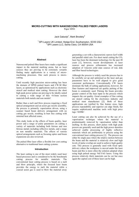
micro-cutting with nanosecond pulsed fiber lasers - BFI Optilas
micro-cutting with nanosecond pulsed fiber lasers - BFI Optilas
micro-cutting with nanosecond pulsed fiber lasers - BFI Optilas

Create successful ePaper yourself
Turn your PDF publications into a flip-book with our unique Google optimized e-Paper software.
MICRO-CUTTING WITH NANOSECOND PULSED FIBER LASERS<br />
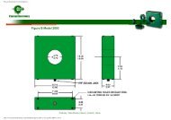
Paper M901<br />
Jack Gabzdyl 1 , Mark Brodsky 2<br />
1 SPI Lasers UK Limited, Hedge End, Southampton, SO30 2QU<br />
2 SPI Lasers LLC, Santa Clara, CA 95054 USA<br />
Abstract<br />
Nanosecond <strong>pulsed</strong> <strong>fiber</strong> <strong>lasers</strong> have made a significant<br />
impact in the material marking arena, but as laser<br />
sources they are proving to be extremely versatile<br />
finding many applications in a variety of <strong>micro</strong>machining<br />
processes. One such process is <strong>micro</strong><strong>cutting</strong>.<br />
Until recently high precision <strong>micro</strong>-<strong>cutting</strong> has been<br />
the domain of DPSS <strong>pulsed</strong> <strong>lasers</strong> and CW-M <strong>fiber</strong><br />
<strong>lasers</strong>, as epitomised by applications such as electronic<br />
stencil and medical stent <strong>cutting</strong>. However the short<br />
high peak power pulses are proving to be ideally suited<br />
to <strong>cutting</strong> a wide range of thin $200k!<br />
Laser <strong>cutting</strong> can also be achieved by the use of a<br />
vaporisation technique where the material is<br />
predominantly removed by vaporisation rather than<br />
melting. In this process, short pulses <strong>with</strong> high peak<br />
powers are generally used and the high power densities<br />
achieved enable processing of highly reflective<br />
materials which are problematic to process using the<br />
conventional laser <strong>cutting</strong> process [1]. The process can<br />
either be single pass where the relative motion between<br />
the beam and the material is relatively slow and high<br />
levels of pulse overlap are used to achieve high quality<br />
cuts. This process is generally used <strong>with</strong> fixed optic<br />
delivery where the workpiece is moved under the laser<br />
beam and this is more often the solution adopted when<br />
using high <strong>pulsed</strong> energy Nd:YAG <strong>lasers</strong>. Using this<br />
process relatively thick materials can be cut but once<br />
again the capital cost of these laser can be high.
An alternative is to use a multi pass <strong>cutting</strong> process<br />
utilising high speed scanners to repeatedly pass over<br />
the cut line removing a small amount of material per<br />
pass. This technique offers a flexible, accurate and<br />
very affordable solution. The equipment is basically a<br />
simple laser marking system!<br />
Nanosecond <strong>pulsed</strong> <strong>fiber</strong> <strong>lasers</strong> are ideally suited to<br />
this vapour <strong>cutting</strong> process as they are low cost,<br />
compact, reliable and require no maintenance. The<br />
short pulses and relatively high peak powers that can<br />
be achieved <strong>with</strong> directly modulated seed MOPA<br />
designs enable these <strong>lasers</strong> to be effective <strong>cutting</strong> tools.<br />
Optical Considerations<br />
The vaporisation <strong>cutting</strong> process relies on an incident<br />
power density that will achieve a predominantly<br />
vaporisation response from the material. Although a<br />
small spot size is a key attribute of the process it is not<br />
the only beam characteristic that needs to be<br />
considered.<br />
Spot size<br />
The spot size is influenced by three things:<br />
The Focal length of the processing lens<br />
The incident diameter of the laser beam<br />
The beam quality (M 2 )<br />
M2 1.3 1.9 3.2<br />
100mm FL 22 32 53<br />
160mm FL 35 51 85<br />
254mm FL 55 80 135<br />
Figure 1 Effect of F-Ø focal length and beam quality<br />
on calculated spot size (µm) based on 8mm beam<br />
diameter.<br />
Beam Characteristics<br />
Although beam quality is often defined by the M 2<br />
value the impact of the beam related characteristics are<br />
far broader. As shown in Figure 2 the M 2 has a direct<br />
correlation to the spot size, however, pulse<br />
characteristics such as the pulse energy, peak power<br />
and duration also have a significant bearing on the<br />
process.<br />
Laser<br />
model<br />
Beam<br />
Quality<br />
Mode<br />
Pulse<br />
energy<br />
Peak<br />
power<br />
Spot<br />
size<br />
Depth<br />
of field<br />
SM HS HM<br />
Image 1 1mm diameter holes cut in painted steel. Left:<br />
20W SM - M 2
Care need to be taken in the programming to ensure<br />
that the finished part has acceptable finished<br />
dimensions. One point to note is that on the thicker<br />
materials there can be a noticeable taper on the cut<br />
edge ~2-3°.<br />
Using such techniques a wide range of materials and<br />
thicknesses can be cut (Image 3)<br />
Image 3 Cut samples include: 1.2 mm aluminium<br />
sheet, 0.2 mm tinned steel sheet 0.5 mm & 2.0 mm<br />
anodised aluminium courtesy of Newson Engineering<br />
NV.<br />
Materials Cut<br />
This <strong>cutting</strong> process can be applied to a wide variety of<br />
materials ranging from ferritic and non ferrous metals<br />
to ceramics, polymers and carbon composites. The<br />
<strong>cutting</strong> speeds that can be achieved vary quite<br />
considerably from >10 m/min for thin foils to<br />
1mm materials. Compared to<br />
conventional laser <strong>cutting</strong> these speeds may be slow<br />
but for many applications the low capital cost and the<br />
flexibility offered by ns <strong>pulsed</strong> <strong>fiber</strong> laser<br />
<strong>cutting</strong>/marking systems are highly attractive.<br />
Stainless steel<br />
Stainless steel is a widely used material particularly in<br />
the medical industry where there are significant fine<br />
<strong>cutting</strong> requirements. Cutting speeds of >20mm/min<br />
can be achieved <strong>with</strong> good quality in 0.5mm thick 304<br />
grade material [4].<br />
Using a 40W HM laser <strong>with</strong> a fixed <strong>cutting</strong> head and<br />
coaxial assist gas >1.5m/min cut speeds in 200µm<br />
stainless steel can be achieved (Image 4).<br />
Image 4 200µm thick stainless steel sheet cut <strong>with</strong><br />
40W HM at 1.5m/min<br />
Highly Reflective materials<br />
Copper, brass silver and gold have an extremely high<br />
reflectivity and conductivity and are therefore<br />
considered difficult materials to cut. High power<br />
densities are required to initiate the <strong>cutting</strong> process and<br />
this is readily cut <strong>with</strong> ns <strong>fiber</strong> <strong>lasers</strong>.<br />
Brass is a material that is typically considered to be<br />
difficult to cut <strong>with</strong> <strong>lasers</strong> and is often used as a test<br />
material to develop parameters for <strong>cutting</strong> gold. With<br />
sufficient peak power in the pulses excellent cut<br />
quality can be achieved in relatively thick material up<br />
to 1mm <strong>with</strong> 20W HS and 2mm <strong>with</strong> 40W HM (Image<br />
5)<br />
Image 5 Brass sheet cut <strong>with</strong> 20W HS 0.8mm thick in<br />
7min image courtesy of Orotig srl<br />
The <strong>cutting</strong> of copper has many applications<br />
particularly in the electrical and electronics areas<br />
particularly of foil type materials. An emerging<br />
application is the <strong>cutting</strong> of copper deposited tracks on<br />
PCB boards where there are requirements to cut<br />
conductive tracks on the boards.<br />
The <strong>cutting</strong> of precious metals such as silver and gold<br />
are increasingly being done using <strong>pulsed</strong> <strong>lasers</strong>. The<br />
ability to do intricate patterns <strong>with</strong> very low material<br />
wastage is highly attractive to the jewellery sector. As<br />
an example a high quality ornately patterned silver
disk of 20mm diameter has been cut using a 20W HS<br />
laser (Image 6).<br />
Image 6 Silver disc 0.55mm thick cut <strong>with</strong> 20W in<br />
13minutes image courtesy of Orotig srl<br />
Silicon <strong>cutting</strong><br />
Silicon is a material that is widely used in the<br />
electronics and solar industries and here are numerous<br />
<strong>cutting</strong> applications. This material is conventionally<br />
diced or cut using mechanical diamond <strong>cutting</strong> wheels,<br />
however these have limitations on thinner materials<br />
and do suffer from chipping at the cut edges. The<br />
<strong>pulsed</strong> laser offers a flexible alternative that can to<br />
used to cut complex profiles and shapes <strong>with</strong> ease. The<br />
5mm squares were cut out in 6sec using 20W SM<br />
(Image 7)<br />
Image 7 Squares cut from 200µm thick polycrystalline<br />
silicon sample courtesy of University of Lisbon,<br />
Faculty of Sciences<br />
Ceramic <strong>cutting</strong><br />
There is a significant industrial requirement for <strong>cutting</strong><br />
of ceramics. Within the electronics industry there is a<br />
lot of thin substrate material that is cut either through<br />
scribe and break or through <strong>cutting</strong>. Again the<br />
limitation is the absorption of the material. The key<br />
materials are alumina and aluminium nitride and their<br />
ability to be cut <strong>with</strong> 1µm <strong>lasers</strong> depends on the<br />
specific material and surface finish. An example that<br />
processes well is green AlN where small discs can be<br />
rapidly cut from substrates (Image 8).<br />
Image 8 ALN green ceramic 3mm thick cut <strong>with</strong> 40W<br />
HM laser using 6 passes at 50mm/s<br />
Non metallic <strong>cutting</strong><br />
The <strong>pulsed</strong> laser can also be used to cut a wide range<br />
of non metallic materials such as plastics and even<br />
rubbers. A key factor in determining if a material can<br />
be cut is the level of the absorption of the material to<br />
1µm laser light. Many plastics have high transmission<br />
at this wavelength and are therefore not suitable,<br />
however, some materials can be cut. An example is<br />
plastic labels which can be marked as well as cut out<br />
from the sheet <strong>with</strong> a simple change in processing<br />
parameters (Image 9)<br />
Image 9 Marking and <strong>cutting</strong> outline of labels in heat<br />
shrink material samples courtesy of Thinklaser<br />
Composite materials<br />
Composites such as carbon <strong>fiber</strong> materials can be cut<br />
in thicknesses in excess of 1mm however, processing<br />
conditions need to be tailored to the material as some<br />
are more sensitive to charring. Perhaps another<br />
alternative is the <strong>cutting</strong> of multilayer materials. An<br />
interesting application is in the electronics industry<br />
where 20W HS <strong>lasers</strong> are used for component crosssectioning.<br />
The flexibility of the laser allows all of the<br />
different material layers to be cut successfully (Image<br />
10)
Image 10 An IC chip sectioned <strong>with</strong> 20W HS laser to<br />
show the various layers<br />
Summary<br />
Nanosecond <strong>pulsed</strong> <strong>fiber</strong> <strong>lasers</strong> are ideally suited to<br />
vaporisation <strong>cutting</strong> applications. This paper highlights<br />
some specific techniques that can be adopted in<br />
improve cut quality and the material thickness range<br />
and the impact that beam quality can have. A diverse<br />
range of materials can be successfully cut showing the<br />
extreme versatility of these sources.<br />
References<br />
[1] John Powell CO2 Laser Cutting, Springer London<br />
Ltd; 2nd Revised edition (Jun 1998) ISBN-10:<br />
1852330473<br />
[2] P Harrison, A Appleyard, “Fiber class”, Medical<br />
Device Developments, Vol 1 2010<br />
[3]J Gabzdyl, “Marking and <strong>micro</strong>-machining <strong>with</strong><br />
<strong>nanosecond</strong> <strong>pulsed</strong> <strong>fiber</strong> <strong>lasers</strong>” Proc. Int. Conf.<br />
ICALEO 2009 Orlando USA.<br />
[4] Hongqiang Chen , Geoff Shannon, Precision<br />
<strong>cutting</strong> and drilling metals <strong>with</strong> a <strong>fiber</strong> laser marker,<br />
Proc. Int. Conf. ICALEO 2009 Orlando USA.<br />
Meet the Author(s)<br />
Dr Jack Gabzdyl is the Product Line Manager at SPI<br />
Lasers for <strong>pulsed</strong> <strong>lasers</strong> and has over 20 years of laser<br />
materials processing experience. He obtained his PhD<br />
in laser processing from Imperial College London in<br />
1989. He has since had a number of technical and<br />
marketing positions at BOC Gases, Advanced Laser<br />
Solutions and TWI before joining SPI in 2007.<br />
Mark Brodsky is the Manager of the US Applications<br />
Laboratories for SPI Lasers. He was the founder of Mr<br />
Laser Inc, and continues to own and operate Laser<br />
Mark’s Company in San Jose, California. Prior to<br />
joining the laser industry he worked in semiconductor<br />
packaging design and engineering for 15 years.