Create successful ePaper yourself
Turn your PDF publications into a flip-book with our unique Google optimized e-Paper software.
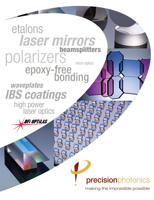
TargetOptical SubstrateZygo NewView200 Surface PlotOptical Bonding. ....... 2Visit our WebsiteVisit our website at www.precisionphotonics.com for a PDF copyof the latest catalog and copies of our technical papers on optics,epoxy-free assembly, IBS coatings, and etalons. On our websiteyou’ll also find application notes, spectral scans and actual laserdamage threshold data to assist you with your optical designsand tolerances.See Us at a Tradeshow or Open House<strong>PPC</strong> hosts open house events and exhibits at industry tradeshowsthroughout the year. Please stop by and visit us, or callto schedule a personalized presentation and tour of our facilities.For the most up-to-date tradeshow schedule, visit our web site atwww.precisionphotonics.com/tradeshows.asp.Y-Direction (mm)0.200.150.100.05Ion Source0.000.00SputteredMaterial0.100.20X-Direction (mm)0.0Coating Information .... 3-0.5-1.0-1.5Precision Metrology .... 4-2.0-2.5Custom Manufacturing. . 50.30nmEtalons. ............ 6–7Government Contracting Made SimpleLaser Mirrors. ...... 8–11As both a government contractor and subcontractor, we have theinfrastructure in place to make your proposal or contract a success.It is straightforward to set us up as a pre-approved vendorbecause we already have transparent billing practices, federallynegotiated indirect rates and government-approved accountingsystems in place. (We are ITAR compliant and a small businessentity.) We understand tight deadlines so we offer fast turnarounds on NDAs and other legal doc uments, statement-of-workwrite ups, and rough-order-of-magnitude estimates.Beamsplitters &Dichroic Mirrors. ...... 12Polarizers . ........ 13–14So call us today to set us up as a pre-approved vendor.How to Contact UsPhone: 303 444 9948Fax: 303 444 9951Waveplates. ......... 15Mail:3180 Sterling CircleBoulder, CO 80301USASolid State LaserOptics. .............. 16E-mail: info@precisionphotonics.comsales@precisionphotonics.comWeb: www.precisionphotonics.comQuality AssuredAs an ISO-9001 certified company, weadhere to strict quality controls so you canbe assured of our commitment to bringing youonly the best products, high-quality volumemanufacturing, and superioron-time delivery.ISO 9001:2008Micro-Optics ......... 17Impossible Optics &Applications. ...... 18–19Information, specifications, and prices in this catalog are subject to change without notice.precisionphotonics.com 1
Epoxy-Free Bonding• Completely adhesive-free optical paths• Coated and Uncoated interfaces• Wide range of materials• Zero thickness bondlines (no residue)Why is CADB ® better?The <strong>PPC</strong> CADB optical bondingtechnology is a “gentler” processthan traditional diffusion bonding,working at much lower temperaturesand without pressure. This allows usto offer solid state laser configurationswith a much wider range of materialsand with unique IBS coatingsintegrated into the assembly. Becauseof the proprietary chemical processingof the surfaces, it is also muchmore durable than standard opticalcontacting, resulting in robust, stablecomponents that can be furtherpolished or coated even after assembly.<strong>PPC</strong> has improved upon standard optical contactingby removing the “black art” from the optical bondingprocess. Our patent-pending Chemically Activated DirectBonding (CADB ® ) technology results in epoxy-freeoptical paths that are 100% optically transparent with negligiblescattering and absorptive losses at the interfaces.It offers bond strengths often times equal to the strengthof the bulk materials being bonded, resulting in assembliesthat are exceptionally durable, reliable and resistantto changes in temperature and humidity. Unlike diffusionbonding, CADB can be used on uncoated surfaces orwith our ion-beam-sputtered dielectric thin films, makingit an ideal process for zero order waveplates, solid statelaser assemblies and polarizing beamsplitters.With CADB, we can bond a variety of materials includingfused silica, doped and undoped YAG, YVO 4 , phosphateglasses, KTP, spinel, silicon and sapphire. Contact usor go online for a current list of materials and materialcombinations. In-house shear testing ensures productioncontrol and quantitative comparison data when usingCADB on new materials.CADB products and components:• Beamsplitter cubes• Planar waveguides• Air-gap etalons• Zero-order waveplates• Laser rods with endcapsVisit our web site atwww.precisionphotonics.comfor data and links to our technicalpapers on epoxy-free bonding.• Custom monolithic assemblies• Microchip and thin disk lasers• Polarizing beam combiners2precisionphotonics.com
At <strong>PPC</strong>, Metrology MattersAdhesive-FreeBonding—Optical Contactingof Beamsplitter & EtalonNomarski Microscope Surface ImagesCustomizationto OEM PackagingDual-PortBeamsplitter5Å fused silicaDifferential Interference Contrast Microscopy (DICM) Images of standard and superpolishedsurfaces. The method shown here is also known as Nomarski imaging—a primary tool used forcharacterizing sub-Angstrom surfaces.The manufacturing of precision optical components requiresstate of the art metrology. At <strong>PPC</strong>, we have developed advancedmethods to measure the optical properties of ourdevices because measurement is fundamental to everythingwe do. Whether testing reflectivity to 99.99%, verifyingparallelism to less than 0.1 arc seconds or actually certifyingthe maximum energy thresholds of our coatings, we believeExamples of some of our in-house capabilities are shownhere.AdvancedIon-Beam-Sputtered CoatingsCustom Optical Assemblies—From 10 to 100,000+ PiecesOne of our most successful products, theControlFREQ TM , is a Telcordia-qualifiedwavelength locker for network-deployabletunable lasers. It consistsof a high-precision etalon opticallyCADB ® bonded to a dual0.5Å sapphirenon-polarizing beamsplitter.We designed themicro-optic tothat the numbers don’t lie. <strong>PPC</strong> also partners with universitiesand national laboratories to access the most advancedmeasurement tools in order to provide you with the mostaccurate and complete information available.Thickness measurements taken with our NISTtraceableSW1500 tunable laser spectrum analyzerconfirm total thickness variations (TTV) as low as11nm across a 68 mm diameter—a parallelism ofless than < 0.05 arcseconds!Transmitted wavefront distortion (TWD) througha 12.7 mm beamsplitter cube taken over a clearaperture of 85%. The data shows a wavefront errorof less than λ/20 peak-to-valley and less than λ/100RMS at 633 nm.4 precisionphotonics.com
High-PrecisionEtalon withnm-Level TolerancesElectronic Design& IntegrationPrecision Custom Engineering forVolume ManufacturingHighly RobustTelcordia-QualifiedAssemblyintegrate into a very compact substrate/heat shielding assembly that includes aphotodetector and thermistor. The entireassembly fits into a 14-pin butterflypackage. Each must undergo extensiveenvironmental (temperatureand humidity), shock and vibrationtesting. <strong>PPC</strong> supplies OEM assemblieslike this to a varietyof customers.We bringthe latestscientificadvancesto themanufactureofprecisionoptics sothat we canexceed yourcritical customspecifications andexpectations.State-of-the-Art Metrologywith ±1 nm Precision: the Keyto Repeatable, Scalable Manufacturingfrom 10 to 10,000+ PiecesOur background in building state-of-the-art precisionmeasurement instrumentation has enabled us to pushindustry limits to the nanometer level—and at high volumes.With our proprietary advanced metrology systemsand polishing techniques, we routinely manufacture andmeasure optical thicknesses to ±1 nanometer. In addition,our wafer-based fabrication processes produce opticswith a wedge of less than 40 nm across a 3" diameteroptic—a parallelism of < 0.1 arcseconds! These highprecisionmethods enable us to provide a large volumeof high-quality ultra-precise parts at competitive pricing.Whether it’s a tight spec, tight delivery or quick ramp up,we work with you to make the impossible possible.Full Optical Capabilities—From Polishing and Coatingto System IntegrationWe move quickly and effectively because we uniquelyoffer full complementary in-house capabilities, frompolishing to state-of-the-art metrology.• Manufacturing methods that result in
OpticsNano-Precise : 1-nmToleranced Etalons• ±1-nm opticalthickness accuracies:Nano-Precise• Custom designsincluding VIPA, GT,air-gap and multicavityversions• FSR tolerancesdown to ±0.001 GHz• Custom siliconetalons pg 18Whereas most etalonshave rounded transmissionfunctions, our multi-cavityetalons are available withflat-top filter functions.These Fabry-Perot etalons lead the industry withsuperior free-spectral-range tolerances to astight as ±0.001 GHz and optical thickness accuraciesof ±1 nanometer. They have been suppliedto leading OEM customers and researchersworldwide in telecommunications, aerospace,laser research, and defense.Standard 2x2 mm 2 fused silica etalons are availablefor the 1520–1630-nm wavelength rangewith 50- and 100-GHz nominal FSR values.Solid, air-gap, Gires-Tournois (GT), VIPA, andmulti-cavity versions are also available in a varietyof sizes down to 1×1 mm 2 and a varietyof materials. Multi-cavity versions are bondedusing Chemically Activated Direct Bonding (CADB ® )—an epoxy-free, environmentally robustoptical contact that has passed Telcordiaqualifications. (See page 2 for more informationon CADB.)We characterize each piece in-house to ensureaccuracy in etalon construction and design.Proprietary advanced metrology can measurethicknesses to a precision of one nanometer.Our polishing methods produce optics with awedge of
OpticsEtalon BasicsEtalons forWavelength LockingEtalons are often used for stabilizinga laser’s frequency, or wavelength.In a typical “wavelengthlocker” that uses the side-fringe-lockingtechnique, a portion of the laser’soutput is transmitted through an etalonso that the center wavelength is halfwaydown the side of a transmission peak. Thetechnique takes advantage of the almostlinear slope on either side of the transmissionpeak where frequency variations will belinearly converted into amplitude variations.To eliminate spurious laser amplitude noise,a reference signal from the laser is removedfrom the transmitted etalon signal. The resultingclean signal can then be processedby a feedback control system to adjustthe frequency of the laser. For an exampleof our wavelength-locker designs,see pages 4–5.Etalons are also used as wavelengthreferences, interleavers,and periodic opticalfilters.A Fabry-Perot etalon, often simply called an etalon,is the most basic interferometer and consistsof two flat parallel mirrors separated by adistance L. In a solid etalon, which consists of asingle piece of transparent medium of index ofrefraction n, and thickness L, the incident beamundergoes multiple reflections between the twosurfaces of equal reflectivity R.The transmitted and reflectedsignal is the result ofmultiple-beam interference.The opticalphase acquired onone round trip throughthe etalon is given bywhere is the wavelength ofthe incident light. In a losslesssystem, transmission is 100% when, where m is an integer. Assuming a normalangle of incidence (θ=0˚), the peaks are separatedin frequency (remember that , wherec is the speed of light and is its frequency) bythe free spectral range (FSR) as expressed asThe actual transmitted intensity is expressed aswith .This function F is known as the coefficient of finesse.The transmission T is shown in the figurebelow and is known as the Airy function.As can be seen from the figure, etalons act aswavelength or frequency filters. An importantfigure of merit is the finesse because it defineshow narrow the filtering function is. The finesseis the ratio of the free spectralLrange to the full width at halfnmaximum (FWHM) of thetransmission peak andis directly related to thereflectivity of the surfaceR byThe figure below graphs thetransmission through etalonsof various reflectivities. Devices withhigher reflectivity, thus higher finesse, havenarrower FWHM.Note: the transmitted beam of a higher finesse deviceis the result of interference between beams thattravel many more times through the device. Thus,the physical limitation to the finesse is set by theoverall beam overlap of the etalon as limited by thedeviations of the surfaces from plane parallelism,coating losses, and beam characteristics (angle ofincidence, divergence, beam diameter, etc).Visit our web site atwww.precisionphotonics.comfor a PDF copy of this catalog andcopies of technical papers on:. Etalon Design Basics. Epoxy-Free Optical Bonding. High-Damage-ThresholdCoating TechnologiesNormalized Transmission10.9FSR0.80.70.60.5R=25%0.4FWHM0.3R=50%0.20.1R=90%0190.02 190.04 190.06 190.08 190.1 190.12Optical F r equency (THz )The Airy functions or transmitted intensities ofetalons of various reflectivities as a function offrequency. The higher the reflectivity, the higher thefinesse, and the narrower the FWHM.www.precisionphotonics.com 7
OpticsHigh-Energy Laser-Line Mirrors• R > 99.9% at 0° or45° for both s & p• Ideal for high-powerNd:YAG and fiberlaser applications• Custom reflectivitiesto >99.998%• Fast turn-aroundon custom coatings250 to 3000 nm<strong>PPC</strong> offers superior quality laser mirrors andcoatings at a great value. We use only ion-beamsputtered(IBS) coatings because our IBS coatingsare significantly more dense, durable, andrugged than conventional e-beam or ion-assistedevaporated coatings. Compared to other coatings,IBS coatings also offer lower scatter andabsorption losses and fewer pin-hole defectsin the coated surface. This superior film qualityand uniformity results in environmentally stableoptics with laser damage thresholds exceeding40 J/cm 2 at 1064 nm and 20 ns.For broadband and low dispersion Ti:Sapphiremirrors, see pages 10–11.Need a Custom Mirror—Quickly?We offer full coating design capabilities, rapidprototyping and fast turn of your design—evenin as short as 48 hours.High-Energy Laser-Line Mirrors for 0° IncidenceModel # MI1000-FY MI1000-DY MI1000-TY MI1000-QYTypeHigh-EnergyNd:YAG MirrorsHigh-Energy DoubledNd:YAG MirrorsHigh-Energy TripledNd:YAG MirrorsWavelength 1064 nm 532 nm 355 nm 266 nmHigh-Energy QuadrupledNd:YAG MirrorsReflectivity 99.9% at 0° 99.9% at 0° 99.9% at 0° 99.5% at 0°Clear Aperture 85% 85% 85% 85%Surface Figure* λ/10 λ/10 λ/10 λ/10Surface Quality 10/5 10/5 10/5 10/5Damage Threshold40 J/cm 2 @ 1064 nm20 ns, 20 Hz8 J/cm 2 @ 532 nm10 ns, 20 Hz3 J/cm 2 @ 355 nm10 ns, 20 Hz>2 J/cm 2 @ 266 nm7 ns, 20 HzDurability MIL-PRF-13830B MIL-PRF-13830B MIL-PRF-13830B MIL-PRF-13830BDiameter 1" +0/–0.010" 1" +0/–0.010" 1" +0/–0.010" 1" +0/–0.010"Thickness 1/4" ±0.010" 1/4" ±0.010" 1/4" ±0.010" 1/4" ±0.010"Substrate Material Fused silica Fused silica Fused silica Fused silicaPrice** $145 $145 $185 $190* p-v at 633 nm, after coating with Power subtracted.** For international prices, add 10%.8precisionphotonics.com
OpticsAdvantagesof our Ion-Beam-Sputtered (IBS)Dielectric Thin Films• Durable coatings are easy toclean and chemically resistant• Dense and non-porous structureis insensitive to moisture andother environmental factors• Superior adhesion eliminatesdelamination• Low scatter and absorption lossesresult in high damage thresholdsand long lifetimes• Repeatable, highly controlledprocess for precise layercontrolCall us or go online atwww. precisionphotonics.comfor actual LDT test data!% R% R100.099.599.098.598.097.597.096.596.095.595.0900 950100.099.599.098.598.097.597.096.596.095.51064 nm Mirror 45° AOIs-polp-pol1000 1050 1100 1150 1200 1250 1300Wavelength (nm)532 nm Mirror 45° AOIs-polp-pol95.0450 470 490 510 530 550 570 590 610 630 650Wavelength (nm)% R% R355 nm Mirror 45° AOI100.099.599.098.5s-polp-pol98.097.597.096.596.095.595.0300 320 340 360 380 400 420Wavelength (nm)100.099.899.699.499.299.098.898.698.498.298.0240266 nm Mirror 45° AOIs-polp-pol245 250 255 260 265 270 275 280 285 290Wavelength (nm)High-Energy Laser-Line Mirrors 45° IncidenceModel # MI1045-FY MI1045-DY MI1045-TY MI1045-QYTypeHigh-EnergyNd:YAG MirrorsHigh-Energy DoubledNd:YAG MirrorsHigh-Energy TripledNd:YAG MirrorsWavelength 1064 nm 532 nm 355 nm 266 nmReflectivity99.9% at 45°(both s & p)99.9% at 45°(both s & p)99.5% at 45°(both s & p)Clear Aperture 85% 85% 85% 85%Surface Figure* λ/10 λ/10 λ/10 λ/10Surface Quality 10/5 10/5 10/5 10/5Damage Threshold40 J/cm 2 @ 1064 nm20 ns, 20 Hz8 J/cm 2 @ 532 nm10 ns, 20 Hz3 J/cm 2 @ 355 nm10 ns, 20 HzHigh-Energy QuadrupledNd:YAG Mirrors99.0% at 45°(both s & p)>2 J/cm 2 @ 266 nm7 ns, 20 HzDurability MIL-PRF-13830B MIL-PRF-13830B MIL-PRF-13830B MIL-PRF-13830BDiameter 1" +0/–0.010" 1" +0/–0.010" 1" +0/–0.010" 1" +0/–0.010"Thickness 1/4" ±0.010" 1/4" ±0.010" 1/4" ±0.010" 1/4" ±0.010"Substrate Material Fused silica Fused silica Fused silica Fused silicaPrice** $145 $145 $185 $190* p-v at 633 nm, after coating with Power subtracted.** For international prices, add 10%.precisionphotonics.com9
OpticsWhy DielectricInstead of Metal?Metal mirrors havelong been the standardfor general-purposebroadband high reflectors,but they have severalsignificant limitationswhich make thema poor match for manyof today’s laser applications.Although inexpensiveupfront, drawbacksof metal mirrorsinclude susceptibilityto both laser damageand mechanical abrasions,tarnishing orsurface degradation,and poor adhesion. Incontrast, the increasedreflectivity and durabilityof all-dielectriccoatings could result inimproved performanceand cost savings overthe lifetime of an opticor optical system.<strong>PPC</strong>’s broadband dielectriccoating coversa broad wavelengthrange (350–1100 nm)with > 99% reflectivity,independent of bothangle and polarization.Our high-energyion-beam-sputtering(IBS) process resultsin durable, dense dielectricfilms that havesuperior reflective andmechanical propertiesin addition to beingeasy to clean, scratchresistant and insensitiveto environmentalchanges. With highdamage thresholds andlow scatter and absorptioncoefficients, theyare ideal for frequencydoubled and tripled Nd:YAG lasers, fiber lasersand broadband or tunablelaser applications.10High-Energy Broadband Mirrors• Broadband lasermirrors for UV-NIR• Ideal for tunablelasers, Nd:YAG andfiber laser systems• All-dielectric IBScoating design• Can be used at anyincidence angle0-50°These super broadband mirrors (SBB) are ideal forbeam-steering applications using both the fundamentallaser wavelength and one or more harmonicswithin the same beam path. Becauseit is an all-dielectric design, they can handlethe high laser powers of both CW and pulsedsystems, without limiting the useful angle ofincidence or sensitivity to varying states ofpolarization.Custom mirrors are available on other flatand curved substrates. Also, contact us fordetails on stress-compensated mirrors forλ/10 surface flatness after-coating.High-Energy Broadband MirrorsModel # MI1050-SBB MI1000-VIS MI1000-NIRTypeSuper BroadbandDielectric MirrorsBroadband VisibleDielectric MirrorsBroadband Near-IRDielectric MirrorsWavelength Range 350–1100 nm 350–700 nm 700–1150 nmReflectivityprecisionphotonics.com99% from 0–50°(both s & p)99% from 0–45°(both s & p)Clear Aperture 85% 85% 85%Surface Figure* λ/10 λ/10 λ/10Surface Quality 20/10 20/10 20/10Damage Threshold% R10090080706050403020100350>5 J/cm 2 @ 1064 nm>1 J/cm 2 @ 355 nm20 ns, 20 HzSBB Mirror 350 nm – 1100 nmNormal Incidence45° AOI Random Polarization600 800 1000 1200 1400Wavelength (nm)>2 J/cm 2 @ 532 nm10 ns, 20 Hz99% from 0–45°(both s & p)>8 J/cm 2 @ 1064 nm20 ns, 20 HzDurability MIL-PRF-13830B MIL-PRF-13830B MIL-PRF-13830BDiameter 1" +0/–0.010" 1" +0/–0.010" 1" +0/–0.010"Thickness 1/4" ±0.010" 1/4" ±0.010" 1/4" ±0.010"Substrate Material Fused silica Fused silica Fused silicaPrice** $275 $175 $175* p-v at 633 nm, after coating with Power subtracted.** For international prices, add 10%.
OpticsBroadband Dispersion-Free MirrorsMuntjac skin fibroblast cells withactin filaments labeled by Alexa488. Excitation at 1035 nm. Emissiondetected at 520 nm usingcustom <strong>PPC</strong> mirrors. Courtesyof the University ofChicago Gordon Centerfor IntegrativeScience.For ultrafast Ti:Sapphire and fiberlasers, <strong>PPC</strong> has produced a lineof dispersion-free mirrors anddichroic beamsplitters thatoffer both broadband reflectivityand high laser-damagethresholds. The MPM mirrorhas been speciallydesigned for multi-photonapplications requiring highreflectivity, broad bandwidth,low dispersion andhigh transmission in the visiblespectrum. All our lasermirrors are ion beam sputtered;thus the coatings aredense, easy to clean and insensitiveto moisture.Call for information on custombroadband and low dispersion polarizers.• Ideal for highenergyTi:Sapphireand microscopyapplications• Dispersion-freemirrors andbeamsplitters• Custom beamsplittersand dichroicmirrors available(see pg 12)% TGroup Delay Dispersion (fs 2 )100908070605040302010Multiphoton Microscopy Mirror (MPM)s-polp-pol0350 400 450 500 550 600 650 700 750 800 850 900 950 1000Wavelength (nm)GDD of TiD Mirror 45° AOI100806040200–20–40s-pol–60p-pol–80–100700 750 800 850 900 950 1000 1050Wavelength (nm)High-Energy Dispersion-Free Laser MirrorsModel # MI1000-TiD MI1045-TiD MI1045-MPMTypeDispersion-Free Ti:SapphireMirrors at 0˚Dispersion-Free Ti:SapphireMirrors at 45˚Multiphoton MicroscopyDichroic Mirrors, 45°Wavelength Range 750–940 nm 750–970 nm 730–870 nmReflectivity99.8% at 0°—99.8% at 45°(s only)99.8% at 45°(s only)Avg. Transmission — — >90% (400–650 nm)Clear Aperture 85% 85% 85%Wavefront λ/10 flatness* λ/10 flatness* λ/10 TWDSurface Quality 20/10 20/10 20/10Durability MIL-PRF-13830B MIL-PRF-13830B MIL-PRF-13830BDimensions1" diameter+0/–0.010"1" diameter+0/–0.010"36.0×25.4 mm+0/– 0.127 mmThickness 1/4" ±0.010" 1/4" ±0.010" 1.0 ±0.1 mmSubstrate Material Fused silica Fused silica Fused silicaPrice** $300 $300 $485* p-v at 633 nm, after coating with Power subtracted.** For international prices, add 10%.% R10099989796TiD Mirror 45° AOI95949392s-polp-pol9190700 750 800 850 900 950 1000 1050Wavelength (nm)precisionphotonics.com11
OpticsCustom Beamsplitters andDichroic MirrorsMWIR Coatings(2.94 μm and3–5 μm)<strong>PPC</strong>’s IBS coatingsprovide outstandingperformance for thenew generation ofsolid state lasers operatingat 2 µm (Ho:YAG,Ho:YLF, Tm:fiber,Tm:YAG), 2-3 µm tunablelasers (Cr:ZnSe),and 2.94 µm lasers(Er:YAG).In order to further expandand quantify ourcapabilities, we haveactive R&D projectsand government SBIRprograms for additionalIBS coating developmentthroughout themid-infrared (MWIR)wavelength region(2–5 µm).12% T1009080706050403020100700 750% T800 850 900 950 1000 1050 1100 1150 1200Wavelength (nm)Unpolarized Light30°Fused Silica• Durable IBS coatingsfor precisionspecs and stability• Dichroic mirrorswith R > 99% at l 1and T > 98% at l 2• Anti-reflectioncoating to R < 0.1%Example A: custom dichroic mirrors30°pTFPCoating30°HR CoatingExample B: custom polarizing beamsplitter100908056° AOI, S-pol.56° AOI, P-pol.7060504030201001900 1950 2000 2050 2100 2150 2200 2250Wavelength (nm)Example C: custom 2.1 µm polarizerprecisionphotonics.comAmong the many diverse custom optical componentsthat <strong>PPC</strong> offers are gradient coating mirrors,low dispersion polarizing cubes, diode-pumpedNd:YAG resonator mirrors, 50/50 non-polarizingbeamsplitters and thin-film plate polarizingbeamsplitters. For all the optical componentswe provide, we use only ion-beam-sputtered(IBS) coatings because our IBS coatings aresignificantly more dense, durable, and ruggedthan conventional coatings. The IBS coatingprocess is both accurate and repeatable, resultingin precision coatings that are easy toclean, chemically resistant and insensitive tomoisture and other environmental factors.For broadband, dispersion-free multi-photonmicroscopy mirrors, see page 11.For polarizing beamsplitters, see pages 13–14.These are just some of the types of coatings that <strong>PPC</strong>does every day on in-house and customer-supplied substrates.High-energy ion-beam-sputtered thin films that areaccurate, durable and environmentally stable are ourforté, and we can turn around parts in as little as 48hours!Typical Dichroic CharacteristicsTypeLong-wave pass, short-wave pass orcustomOperating WavelengthUV, Visible & NIR (250–3000 nm)Angle of Incidence0°, 45° or customReflectivity>99.9%Transmission>98%On/Off Tolerance5%AR on Side 2
OpticsPolarizing Beamsplitter CubesNo Glue Here!<strong>PPC</strong> beamsplitter cubes are derived from a unique combination of IBScoatings, ultraprecise fabrication capabilities and our robust, epoxyfreebonding technology—Chemically Activated Direct Bonding (CADB ® ) which results in a zero-bondline thickness and laserdamage thresholds up to three times the power levels of othercommercially available products. In addition to the standardsizes and wavelengths shown, we can produce high-energycube beamsplitters from 1×1 mm 2 in size, and in a wide varietyof materials including fused silica, BK7, YAG, and other opticalglasses and crystals.Whether you need 10 or 10,000 pieces, our precision waferbasedprocesses result in high yields and competitive costs,especially at higher volumes. These high-precision assemblieshave been widely used in telecommunications, semi-conductorand biomedical applications where transmission efficiency, extinctionratio and wavefront quality are all critical specifications.All of our polarizing beamsplitter cubes are epoxy free, making themsuitable for high power applications with energy densities exceeding10 J/cm 2 at 1064 nm.Contact us for information on custom broadband polarizers and low dispersionbeamsplitter cube designs.See page 17 for more information on custom prisms, micro-optics and optical-assemblies.See pages 14–15 for other polarization components such as Brewster plates andwaveplates.• CADB bondingfor epoxy-freeoptical paths• High-energylaser-line designs• Convenient 90°beam separation• Custom cubesavailable from1 mm to >25 mmPolarizing Beamsplitter CubesModel # PBS1010-FY PBS1005-FY PBS1005-DY PBS1005-TYType Laser Line Laser Line Laser Line Laser LineWavelength 1064 nm 1064 nm 532 nm 355 nmReflection Efficiency, R s >99.9% >99.9% >99.85% >99.8%Avg. Transmission, T p >95% >95% >95% >95%Extinction Ratio, T p /T s 1,000:1 1,000:1 750:1 500:1AR Coating
OpticsZero- and Multiple-OrderWaveplatesWaveplates are available as standalonecomponents, or as part of amore complex optical assembly.<strong>PPC</strong> manufactures custom multielementpolarization assembliesin sizes from 1 mm to> 1" for R&D, biomedicaland aerospaceapplications.<strong>PPC</strong> uses laser-grade crystal quartz to produce multiple-order,true zero-order and compound zero-order waveplates with retardationsof quarter-wave, half-wave or anything in-between.Multiple-order retarders are ideal for narrow- or single-wavelengthapplications at a specific operating temperature. For increasedbandwidth and thermal stability, zero-order waveplatesare recommended.For compound zero-order waveplates and multi-element waveplateassemblies, we use durable IBS coatings and our proprietaryepoxy-free bonding technology—Chemically Activated DirectBonding (CADB ® ). This unique combination of processes results inprecise, high-energy components that exhibit environmental stabilityand improved transmitted wavefront characteristics.All of our waveplates and waveplate assemblies are adhesive free, makingthem suitable for high power applications with energy densities exceeding20 J/cm 2 at 1064 nm.Waveplate CharacteristicsModel # WPZ10H-FY WPZ10Q-FYType Compound zero order Compound zero orderRetardation Half wave Quarter waveWavelength 1064 nm 1064 nmMaterial Crystal quartz Crystal quartzRetardation Tolerance ± λ/500 ± λ/500AR Coating
OpticsSolid State Laser OpticsNo Glue Here!<strong>PPC</strong>'s Chemically ActivatedDirect Bonding(CADB ® ) technologyresults in epoxy-freeoptical paths that areperfectly transparentwith negligible scatteringand absorptivelosses at the interfaces.It offers bond strengthsthat are often equalto the strength of thebulk materials beingbonded, making it anexceptionally durableand reliable process.CADB can be used onuncoated surfaces orwith our ion-beamsputtereddielectric thinfilms, making it idealfor monolithic opticaldevices and compositelaser assemblies.• Variety of shapesand sizes availablefrom waveguides tozig-zag slabs andthin disks• Epoxy-free opticalpaths with zerobondline thickness• Coated and uncoatedinterfacesThese high-performance bonded structures for solid-state laser amplifiers and oscillatorsuse our proprietary CADB ® process to achieve adhesive-free, compositecrystal, glass and ceramic structures. Ideal for high-power solid-state laser applicationsfor LIDAR, defense and aerospace, materials processing, and medical industries,these robust devices can be fabricated in a variety of geometries (rod endcaps, laser slabs and disks) and form factors from 1 mm to greater than 100 mm.The CADB process is extremely strong and offers negligible scatter and absorptivelosses at the interfaces; it also works with both IBS coated and uncoated surfaces.Our ion beam sputtered coating technology can handle damage thresholds above40 J/cm² with less than 2 ppm bulk absorption in the coatings, making them suitablefor a wide variety of high power solid state lasers and laser gain media structuresincluding microchip lasers and Q-switch lasers with Cr 4 +:YAG or Co:Spinelsaturable absorbers.For more information on the CADB optical bonding process and links to our technicalpapers, go online to www.precisionphotonics.com and click on Capabilities.Our CADB bonding resultsin zero bond-line thicknessesand TWD < λ/10.Available in a widerange of materialsFused silicaULE, Zerodur ®YAG (doped and undoped,crystalline and ceramic)YVO 4SapphirePhosphate GlassesSpinel (crystal and ceramic)GGGSilicon, SiCQuartzKTPCVD DiamondZnSeTypical Characteristics (to be used as design guidelines only)Operating CharacteristicsHigh-damage-threshold interfaces& coatingsPrecise Gain Medium Dimension*Thickness Uniformity: ±0.3 µmAbsolute Thickness Control: ±0.5 µmMaterialsGain Medium: Laser crystalline andceramic materials (YAG, phosphateglass, etc.)Cladding: Crystalline, glass, and ceramicmaterials (YAG, sapphire, etc.)Custom Thin-Film CoatingsAnti-reflection, partial reflection,high reflection & beamsplittingBond AreasUp to 200 cm 2Angular TolerancesEnd-Face Relative Positioning:30 arcsec typical* All parts come with individual devicemeasurement reports.Custom coatingsavailable on our CADBbonded parts16precisionphotonics.com
OpticsCustom Micro-Optics and AssembliesWhether you need 10 or 10,000 pieces, our precision wafer-based processes resultin high yields and competitive costs, especially at higher volumes. These highqualitycustom optics and optical assemblies combine our IBS coatings, ultraprecisefabrication capabilities and epoxy-free bonding technology—Chemically ActivatedDirect Bonding (CADB ® ) to produce components which are widely used in thetelecommunications, semi-conductor and biomedical industries.Adhesive-free assemblies are ideal for increasing the sensitivity in beam-deliverymicro-systems, fiber-optics, and endoscopic systems used in coherent communications,fluorescence spectroscopy, Raman spectroscopy, optical-coherencetomography (OCT), and microscopy. Because of their miniature size, they can beplaced right at the objective lens or at the tip of optical fibers and light pipes.Call us to discuss your requirements for custom etalons, prisms, cubes, waveplates,polarizing beamsplitters and micro-optic assemblies.Custom Prism & Micro-Optics CharacteristicsOperating WavelengthUV, Visible, NIR, MWIR(250–5000 nm)Dimensional ToleranceDown to ± 25 µmAngle Tolerance±1 minute standardTypical Insertion Loss
ApplicationsImpossible Optics—Applications & ExamplesQuick Ramp-up from 1,000 to 30,000 Units per MonthWhen one of our customers asked us to ramp up from 1,000 to 10,000delivered parts per month—a seemingly impossible task—we reactedquickly and were able to hit the goal in just eight weeks. Several monthslater they asked us to ramp up again from 15,000 to 30,000 units permonth and we met the requirement in just 4 weeks!It wasn’t easy, but by working closely with our customer and ourmanufacturing team, we are now delivering thousands of high-toleranceparts per month and can respond quickly to schedule changes.Our background in building state-of-the-art precision measurementinstrumentation enables us to push industry limits to the nanometerlevel—in this case it was a thickness tolerance of ±100 atoms!Ultra-flat Wafers & EtalonsBy utilizing state-of-the-art metrology, wafer-based optical fabrication andour advanced ion-beam-sputtering (IBS) coatings, we have been able torepeatedly produce ultra-flat, optical grade fused silica, quartz and siliconcomponents. Thickness measurements taken with our laser-based, NISTtraceableSW1500 metrology system confirm total thickness variations(TTV) as low as 11 nm across a 68 mm diameter—a parallelism of lessthan
Monolithic Assemblies with λ/20 TWDApplicationsWe routinely produce optically bonded assemblies withless than 0.05 waves of transmitted wavefront distortion(TWD) peak-to-valley. λ/10 wavefronts are fairly commonon single optical components, but when you buildmulti-element optic assemblies, these distortions cancompound, resulting in much higher levels of distortion.With our nanometer-level tolerances, IBS coatings, andunique zero-bond-length adhesive-free CADB ® bondingprocess, our monolithic optical assemblies consistentlyexceed even the most stringent specificationsincluding λ/20 peak-to-valley TWD, beam deviation < 30arcseconds and optical path lengths matched to betterthan 10 microns.YAG chip laser with cladding on all sidesBuilt in collaboration with the Engineering Research Center for Extreme Ultraviolet(EUV) Science and Technology and Colorado State University.This high-power yttrium aluminum garnet (YAG or Y 3 Al 5 O 12 ) chip laseris a completely epoxy-free assembly comprised of several doped YAGand sapphire components. Manufactured using our patent-pendingCADB ® bonding process and advanced polishing techniques, thispart required several iterative processing steps, thus highlighting theimportance of robust, durable bonds and meticulous cleaning andhandling techniques. From the raw material specifications through thefinal metrology, we worked together with the customer to meet theirbudgetary requirements and performance expectations for the final,coated assembly.Superpolished Sapphire to < 1Å RMSOnce our customers found out that we can polish andmeasure fused silica surfaces to < 1 angstrom in RMSsurface roughness, they immediately asked us if wecould do the same thing on sapphire. Within just a fewweeks we were able to refine our polishing and cleaningprocesses to achieve similar surface quality on not justsapphire (shown here), but Ti:sapphire and TGG crystalas well.Super-polished or laser quality polished substrates andassemblies are ideal for use as low-loss laser mirrors,high energy waveguides and in cavity ring-down spectroscopy(CRDS) where thermal stability, surface scatterand high laser damage thresholds are key requirements.precisionphotonics.com19
Terms and ConditionsFor a complete listing of our terms and conditions, goonline www.precisionphotonics.com.ShipmentsDelivery will be made F.O.B. <strong>PPC</strong>, Boulder, CO, USA. Inthe absence of specific shipping instructions, <strong>PPC</strong> willship by the method it deems most advantageous. Transportationcharges will be prepaid and invoiced.Overseas ShipmentsAll quotations are in US dollars. Parts will be shippedvia customer-specified international carrier againstcustomer-provided account number. All shipping, insuranceand any applicable tariffs and duties will be invoicedto that account.For the convenience of working in your time zone andlanguage, or for assistance regarding customs and importissues, please contact one of our international distributors.An updated list of sales representatives can be foundonline at www.precisionphotonics.com/distributors.Terms Of PaymentAll payments are due net thirty (30) days after theoriginal shipment date.All major credit cards are accepted.Limited Warranty<strong>PPC</strong> warrants that all catalogue products comply withapplicable specifications and will operate under properuse and normal conditions for a period of one year fromdate of delivery.ISO 9001:2008<strong>PPC</strong> adheres to ISO 9001:2008 quality standard. Pleasevisit www.precisionphotonics.com/ISO to view our registrationcertificate.Contact InformationPhone: 303 444 9948Fax: 303 444 9951Mail:3180 Sterling CircleBoulder, CO 80301USAE-mail: info@precisionphotonics.comsales@precisionphotonics.comWeb:www.precisionphotonics.com20 precisionphotonics.com
Converting dBm to mWOptical power is commonlyexpressed inmW or dBm. The dBmunit is defined as theratio in dB (decibel) ofthe measured opticalpower to a referencevalue of 1 mW.For a quick reference,use the following table.OpticalPower(dBm)OpticalPower(mW)15 31.614 25.113 20.012 15.811 12.610 10.09 7.98 6.37 5.06 4.05 3.24 2.53 2.02 1.61 1.30 1.0–1 0.79–2 0.63–3 0.50–4 0.40–5 0.32–6 0.25–7 0.20–8 0.16–9 0.13–10 0.10–11 0.08–12 0.06–13 0.05–14 0.04–15 0.03Snell’s Lawn 11n 22International System of Units(SI) PrefixesFactor Name Symbol10 21 zetta Z10 18 exa E10 15 peta P10 12 tera T10 9 giga G10 6 mega M10 3 kilo k10 2 hecto h10 -2 centi c10 -3 milli m10 -6 micro µ10 -9 nano n10 -12 pico p10 -15 femto f10 -18 atto a10 -21 zepto z10 -24 yocto yBrewster’s AngleThe angle where only s-polarized lightis reflectedTotal Internal Reflection Anglewhere n transmitted medium< n incident mediumis required for total internal reflection.Etalon FormulasTwo parameters completelyspecify an etalon: the free spectralrange (FSR) and the finesse( ). The FSR is the spacing(usually given in frequency) betweentransmission peaks. Thefinesse is the ratio of the freespectral range to the full widthat half maximum (FWHM) of thetransmission peak and is directlyrelated to the reflectivity of thesurface R.c is the speed of light, n is theindex of refraction of the etalon,and L is the thickness of theetalon.www.precisionphotonics.comphone: 303 444 9948Physical Constantsh =Planck’s constant=6.626 x 10 -27 erg•s= 6.626 x 10 -34 J•s=4.5 x 10 -15 eV•sh =h/2 =Dirac’s constant=1.054 x 10 -27 erg•s=1.054 x 10 -34 J•sk =Boltzmann’s constant = 1.380 x 10 -16 erg/K= 8.62 x 10 -5 eV/K=1.380 x 10 -23 J/KkT=25.9 meV at room temperature=6.7 meV at liquid-nitrogen temperature (77 K)=0.36 meV at liquid-helium temperature (4.2 K)c=velocity of light in vacuum=2.998 x 10 8 m/s(Note: the exact value is 2.99792458 x 10 8 m/s)e =electron charge=1.602 x 10 -19 coulombs= 4.803 x 10 -10 esuN o =Avogadro’s number=6.023 x 10 23 molecules/g-moleα o =h 2 /4 me 2 =first Bohr radius=5.292 x 10 -11 mε o =permittivity constant=8.854 x 10 -12 F/mµ o =permeability constant=1.257 x 10 -6 H/mm e =electron rest mass=9.109 x 10 -31 kgm p =proton rest mass=1.672 x 10 -27 kg# of seconds in a year~ x 10 7At high finesse values(where R is very close to100% or 1),Finesse Reflectivity2 24%4 47%6 60%8 68%10 73%15 81%20 85%Numerical ApertureCollimatingdDffDFocusingdFocusing GaussianBeamsA Gaussian beamspreads as follows,where (x) is the 1/e 2 radius, l is thewavelength, and x isthe distance from thebeam waist w 0 wherex=0. A rule of thumbfor choosing a lens iswhere f is the lens focallength, d is the beamdiameter at the focus,D is the 1/e 2 diameterof the collimated beam.Wave Vector, Frequency,Wavelength& Wavenumbersk=wave vectorν=frequencyω=angular frequency=2πνλ=wavelengthλ o =wavelength in vacuumn=refractive indexAn easy number toremember is a 1-pmlinewidth is approximately125 MHz at1550 nm.Common Material PropertiesMaterialRefractiveIndex, nDFSR*Thermal ExpansionCoefficient (α)Thermo-OpticCoefficient (β or )Air 1.000 0.0 MHz 0.0 ppm/˚C 1.0 ppm/˚CFused Silica 1.444 13.1 MHz 0.55 ppm/˚C 6.57 ppm/˚CSilicon 3.477 198.1 MHz 3.25 ppm/˚C 160 ppm/˚CLASFN9 1.813 9.4 MHz 7.4 ppm/˚C 1.3 ppm/˚C*Change in FSR due to dispersive effects as measured from 1510 to 1570 nm for a 50-GHz etalonWavelengthElectronFrequency Wavenumber(in vacuum) Volts1561.42 nm 192.00 THz 0.80 eV 6,404.43 cm -11550 nm 193.41 THz 0.80 eV 6,451.61 cm -11320 nm 227.12 THz 0.94 eV 7,575.76 cm -11064 nm 281.76 THz 1.17 eV 9,398.50 cm -1980 nm 305.91 THz 1.27 eV 10,204.08 cm -1780 nm 384.35 THz 1.59 eV 12,820.51 cm -1632.8 nm 473.76 THz 1.96 eV 15,802.78 cm -1350 nm 856.55 THz 3.55 eV 28,571.43 cm -1
making the impossible possible<strong>BFi</strong> <strong>OPTiLAS</strong> Representatives for Precision PhotonicsGermany<strong>BFi</strong> <strong>OPTiLAS</strong> GmbHOppelner Strasse, 5D–82194 Gröbenzell - (Munich) GermanyPhone: +49-(0) 81 42 65 20-0E-mail: sales.de@bfioptilas.comWeb: http://www.photonics.bfioptilas.deFrance<strong>BFi</strong> <strong>OPTiLAS</strong> S.A.S4 allée du CantalZ.I. La Petite Montagne Sud-CE 183491018 EVRY Cedex - FrancePhone: +33-(0) 1 60 79 59 00E-mail: photonique.fr@bfioptilas.comWeb: http://www.photonics.bfioptilas.frUnited Kingdom<strong>BFi</strong> <strong>OPTiLAS</strong> LtdMill Square - Wolverton Mill SouthMilton Keynes - MK 12 5ZY - UKPhone: +44 (0)1908 326 326E-mail: sales.uk@bfioptilas.comWeb: http://www.photonics.bfioptilas.co.ukSpain<strong>BFi</strong> <strong>OPTiLAS</strong> S.LC / Anabel Segura, 7Planta Acceso28108 Alcobendas (Madrid) - SpainPhone: +34-91 453 11 60E-mail: fotonica@bfioptilas.comWeb: http://www.photonics.bfioptilas.esNordic Operation<strong>BFi</strong> <strong>OPTiLAS</strong> A/SPortalgatan, 2B - PO Box 1335S - 75423 Uppsala - SwedenPhone: +46-18 56 58 30E-mail: info.se@bfioptilas.comWeb: http://www.photonics.bfioptilas.seBenelux<strong>BFi</strong> <strong>OPTiLAS</strong> BV(Chr. Huygensweg 17) - PO Box 2222400 AE Alphen aan den RijnThe NetherlandsPhone: +31-(0) 172 44 60 60E-mail: e-o.nl@bfioptilas.comWeb: http://www.photonics.bfioptilas.nlItaly - Rome<strong>BFi</strong> <strong>OPTiLAS</strong> S.R.LVia Emilio de Marchi 2700141 Rome - ItalyPhone: +39 06 86 89 42 59E-mail: info.it@bfioptilas.comWeb: http://www.photonics.bfioptilas.itItaly - Milan<strong>BFi</strong> <strong>OPTiLAS</strong> S.R.LVia Cascina Venina 2020090 Assago (Mi) ItalyPhone: +39 02 535 831E-mail: info.it@bfioptilas.comWeb: http://www.photonics.bfioptilas.it


