OpticsSolid State Laser OpticsNo Glue Here!<strong>PPC</strong>'s Chemically ActivatedDirect Bonding(CADB ® ) technologyresults in epoxy-freeoptical paths that areperfectly transparentwith negligible scatteringand absorptivelosses at the interfaces.It offers bond strengthsthat are often equalto the strength of thebulk materials beingbonded, making it anexceptionally durableand reliable process.CADB can be used onuncoated surfaces orwith our ion-beamsputtereddielectric thinfilms, making it idealfor monolithic opticaldevices and compositelaser assemblies.• Variety of shapesand sizes availablefrom waveguides tozig-zag slabs andthin disks• Epoxy-free opticalpaths with zerobondline thickness• Coated and uncoatedinterfacesThese high-performance bonded structures for solid-state laser amplifiers and oscillatorsuse our proprietary CADB ® process to achieve adhesive-free, compositecrystal, glass and ceramic structures. Ideal for high-power solid-state laser applicationsfor LIDAR, defense and aerospace, materials processing, and medical industries,these robust devices can be fabricated in a variety of geometries (rod endcaps, laser slabs and disks) and form factors from 1 mm to greater than 100 mm.The CADB process is extremely strong and offers negligible scatter and absorptivelosses at the interfaces; it also works with both IBS coated and uncoated surfaces.Our ion beam sputtered coating technology can handle damage thresholds above40 J/cm² with less than 2 ppm bulk absorption in the coatings, making them suitablefor a wide variety of high power solid state lasers and laser gain media structuresincluding microchip lasers and Q-switch lasers with Cr 4 +:YAG or Co:Spinelsaturable absorbers.For more information on the CADB optical bonding process and links to our technicalpapers, go online to www.precisionphotonics.com and click on Capabilities.Our CADB bonding resultsin zero bond-line thicknessesand TWD < λ/10.Available in a widerange of materialsFused silicaULE, Zerodur ®YAG (doped and undoped,crystalline and ceramic)YVO 4SapphirePhosphate GlassesSpinel (crystal and ceramic)GGGSilicon, SiCQuartzKTPCVD DiamondZnSeTypical Characteristics (to be used as design guidelines only)Operating CharacteristicsHigh-damage-threshold interfaces& coatingsPrecise Gain Medium Dimension*Thickness Uniformity: ±0.3 µmAbsolute Thickness Control: ±0.5 µmMaterialsGain Medium: Laser crystalline andceramic materials (YAG, phosphateglass, etc.)Cladding: Crystalline, glass, and ceramicmaterials (YAG, sapphire, etc.)Custom Thin-Film CoatingsAnti-reflection, partial reflection,high reflection & beamsplittingBond AreasUp to 200 cm 2Angular TolerancesEnd-Face Relative Positioning:30 arcsec typical* All parts come with individual devicemeasurement reports.Custom coatingsavailable on our CADBbonded parts16precisionphotonics.com
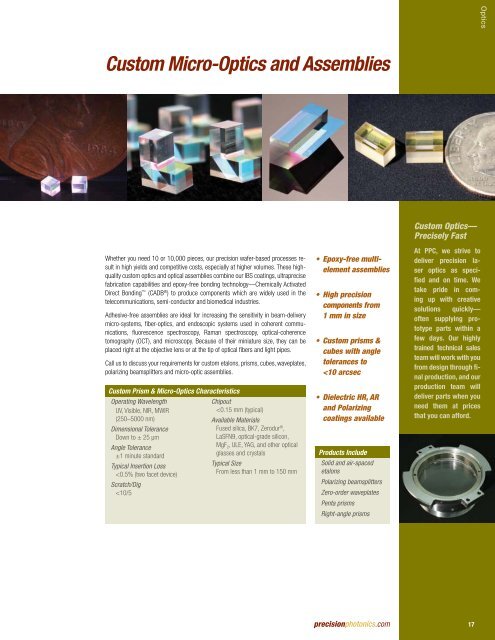
OpticsCustom Micro-Optics and AssembliesWhether you need 10 or 10,000 pieces, our precision wafer-based processes resultin high yields and competitive costs, especially at higher volumes. These highqualitycustom optics and optical assemblies combine our IBS coatings, ultraprecisefabrication capabilities and epoxy-free bonding technology—Chemically ActivatedDirect Bonding (CADB ® ) to produce components which are widely used in thetelecommunications, semi-conductor and biomedical industries.Adhesive-free assemblies are ideal for increasing the sensitivity in beam-deliverymicro-systems, fiber-optics, and endoscopic systems used in coherent communications,fluorescence spectroscopy, Raman spectroscopy, optical-coherencetomography (OCT), and microscopy. Because of their miniature size, they can beplaced right at the objective lens or at the tip of optical fibers and light pipes.Call us to discuss your requirements for custom etalons, prisms, cubes, waveplates,polarizing beamsplitters and micro-optic assemblies.Custom Prism & Micro-Optics CharacteristicsOperating WavelengthUV, Visible, NIR, MWIR(250–5000 nm)Dimensional ToleranceDown to ± 25 µmAngle Tolerance±1 minute standardTypical Insertion Loss