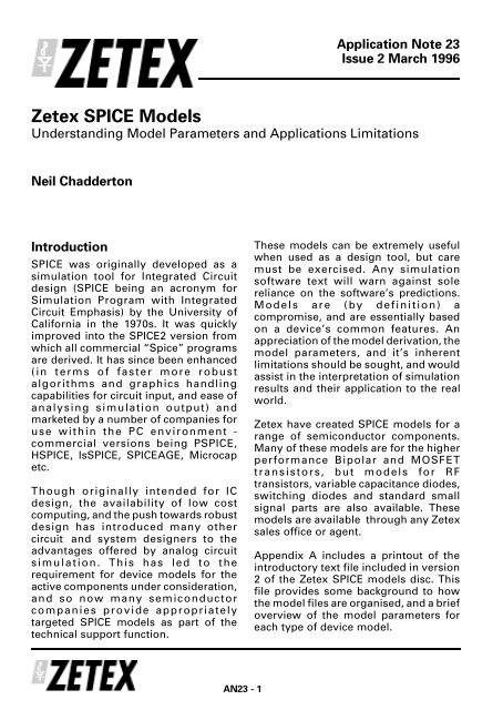
Zetex - AN23 - Zetex SPICE models - understanding ... - Diodes, Inc.
Zetex - AN23 - Zetex SPICE models - understanding ... - Diodes, Inc.
Zetex - AN23 - Zetex SPICE models - understanding ... - Diodes, Inc.

Create successful ePaper yourself
Turn your PDF publications into a flip-book with our unique Google optimized e-Paper software.
<strong>Zetex</strong> <strong>SPICE</strong> Models<br />
Neil Chadderton<br />
Introduction<br />
<strong>SPICE</strong> was originally developed as a<br />
simulation tool for Integrated Circuit<br />
design (<strong>SPICE</strong> being an acronym for<br />
Simulation Program with Integrated<br />
Circuit Emphasis) by the University of<br />
California in the 1970s. It was quickly<br />
improved into the <strong>SPICE</strong>2 version from<br />
which all commercial “Spice” programs<br />
are derived. It has since been enhanced<br />
(in terms of faster more robust<br />
algorithms and graphics handling<br />
capabilities for circuit input, and ease of<br />
analysing simulation output) and<br />
marketed by a number of companies for<br />
use within the PC environment -<br />
commercial versions being P<strong>SPICE</strong>,<br />
H<strong>SPICE</strong>, Is<strong>SPICE</strong>, <strong>SPICE</strong>AGE, Microcap<br />
etc.<br />
Though originally intended for IC<br />
design, the availability of low cost<br />
computing, and the push towards robust<br />
design has introduced many other<br />
circuit and system designers to the<br />
advantages offered by analog circuit<br />
simulation. This has led to the<br />
requirement for device <strong>models</strong> for the<br />
active components under consideration,<br />
and so now many semiconductor<br />
companies provide appropriately<br />
targeted <strong>SPICE</strong> <strong>models</strong> as part of the<br />
technical support function.<br />
Application Note 23<br />
Issue 2 March 1996<br />
Understanding Model Parameters and Applications Limitations<br />
<strong>AN23</strong> - 1<br />
These <strong>models</strong> can be extremely useful<br />
when used as a design tool, but care<br />
must be exercised. Any simulation<br />
software text will warn against sole<br />
reliance on the software’s predictions.<br />
Models are (by definition) a<br />
compromise, and are essentially based<br />
on a device’s common features. An<br />
appreciation of the model derivation, the<br />
model parameters, and it’s inherent<br />
limitations should be sought, and would<br />
assist in the interpretation of simulation<br />
results and their application to the real<br />
world.<br />
<strong>Zetex</strong> have created <strong>SPICE</strong> <strong>models</strong> for a<br />
range of semiconductor components.<br />
Many of these <strong>models</strong> are for the higher<br />
performance Bipolar and MOSFET<br />
transistors, but <strong>models</strong> for RF<br />
transistors, variable capacitance diodes,<br />
switching diodes and standard small<br />
signal parts are also available. These<br />
<strong>models</strong> are available through any <strong>Zetex</strong><br />
sales office or agent.<br />
Appendix A includes a printout of the<br />
introductory text file included in version<br />
2 of the <strong>Zetex</strong> <strong>SPICE</strong> <strong>models</strong> disc. This<br />
file provides some background to how<br />
the model files are organised, and a brief<br />
overview of the model parameters for<br />
each type of device model.
This application note is a guide to the<br />
<strong>understanding</strong> and use of <strong>Zetex</strong> <strong>SPICE</strong><br />
<strong>models</strong>. It includes sections on how<br />
some of these <strong>models</strong> are derived - the<br />
measurements/optimisation necessary,<br />
how to customise <strong>models</strong> for those<br />
cases where a model is not available,<br />
and the limitations to be aware of.<br />
Measurement of Model<br />
Parameters<br />
The bipolar transistor circuit model used<br />
by the <strong>SPICE</strong> software is a modified<br />
version of the Gummel-Poon model<br />
formulated in 1970. The schematic of<br />
this model is shown in Figure 1. For a<br />
comprehensive description of the<br />
model, including physical definitions of<br />
the model components, please refer to<br />
Appendix B, references 1 and 2.<br />
Figure 2 shows a typical model for a<br />
<strong>Zetex</strong> bipolar transistor.<br />
Lines beginning with an asterisk indicate<br />
a non-executable comment; so device<br />
details, date of creation, line spaces, and<br />
copyright messages all start with this<br />
symbol.<br />
B<br />
r'b<br />
B'<br />
CJC<br />
CJE<br />
CDC<br />
CDE<br />
Figure 1<br />
Gummel-Poon Bipolar Transistor Model.<br />
E'<br />
C'<br />
C<br />
E<br />
r'c<br />
r'e<br />
<strong>AN23</strong> - 2<br />
Application Note 23<br />
Issue 2 March 1996<br />
The line beginning “.MODEL ....” uses a<br />
standard <strong>SPICE</strong> command that defines a<br />
model to the software. Following this<br />
command are the device name, it’s<br />
polarity, and a list of the model<br />
parameters - the “+” sign being used for<br />
concatenation to the original command.<br />
The text file reproduced in appendix A<br />
gives some brief details as to the effects<br />
each parameter has on the model’s<br />
behaviour.<br />
The measurements necessary to derive<br />
the bipolar transistor model parameter<br />
values can conveniently be separated<br />
into dc and ac parameters as shown in<br />
table 1. The dc parameters are further<br />
separated into those for forward and<br />
reverse operation. The parasitic<br />
resistance components, and the<br />
saturation current IS being common for<br />
both forward and reverse modes. The<br />
descriptions of the forward parameters<br />
given below is equally applicable to the<br />
reverse parameters. (Appendix B<br />
reference 3).<br />
dc ac<br />
forward reverse<br />
IS CJC<br />
NF NR CJE<br />
BF BR MJC<br />
IKF IKR VJC<br />
VAF VAR MJE<br />
ISE ISC VJE<br />
NE NC TF<br />
RB<br />
RE<br />
RC<br />
TR<br />
Table 1<br />
Bipolar Transistor Model Parameters.
An explanation of the function of the dc<br />
parameters is most easily accomplished<br />
with reference to a chart - sometimes<br />
referred to as the “Gummel Plot”.<br />
Figure 3 shows a Gummel plot, which<br />
illustrates the variation in collector and<br />
base currents with base-emitter voltage<br />
- a requirement being that the device is<br />
on the edge of saturation, satisfied by<br />
VBC = 0, (or VCE= VBE). The collector<br />
current IC (ideally) follows the Shockley<br />
equation that defines the current<br />
through a P-N junction:<br />
I = Is [e qV f<br />
KT −1]<br />
where<br />
IS - the transistor saturation current and<br />
is dependent on the size of the<br />
base-emitter area<br />
k - Boltzmann’s constant=1.38 x 10 -23 J/K<br />
q - electronic charge=1.602 x 10 -19 C<br />
T - temperature in Kelvin, (300K is a<br />
common assumption)<br />
VF - is the voltage across the junction.<br />
With reference to the chart, IS is the<br />
y-axis intercept of the collector current<br />
curve at VBE= 0, and NF defines the slope<br />
of the line (referred to q/kT), and within<br />
Application Note 23<br />
Issue 2 March 1996<br />
*ZETEX ZTX688B Spice model Last revision 8/11/90<br />
*<br />
.MODEL ZTX688B NPN IS = 1.09E-12 NF = 0.9935 BF = 1180 IKF= 5.2 VAF= 25<br />
+ ISE=1.3E-13 NE =1.35 NR =0.992 BR =790 IKR=.5 VAR=5 ISC=0.174E-12<br />
+ NC =1.399 RB = .3 RE =.036 RC = .034 CJC= 104E-12 MJC= .29 VJC= .46<br />
+ CJE=280E-12 TF = .93E-9 TR =1.05E-9<br />
*<br />
Figure 2<br />
General Format of <strong>Zetex</strong> (Bipolar Transistor) <strong>SPICE</strong> Models.<br />
<strong>AN23</strong> - 3<br />
<strong>SPICE</strong> defaults to unity. At high currents,<br />
the collector current differs from that<br />
predicted by the equation due to<br />
resistances, and high level injection<br />
effects. These effects are<br />
accommodated within <strong>SPICE</strong> by<br />
allowing base-emitter de-biasing by the<br />
parasitic emitter resistance (or collector<br />
resistance for the reverse mode), and by<br />
the collector “knee” current parameter,<br />
IKF. (IKF is defined as the collector<br />
current at which the current gain= BF/2,<br />
see below).<br />
The base current (IB) plot would ideally<br />
be parallel to the collector current, the<br />
plot separation being IS/BF, however<br />
there are a number of physical effects<br />
that are addressed by other parameters.<br />
At low values of collector current,<br />
surface leakage and recombination<br />
effects introduce an additional slope to<br />
the plot of IB, causing the line to intercept<br />
the y axis at a higher position than would<br />
be the case if IB was always a fixed<br />
fraction of IC. These effects are described<br />
by two additional <strong>SPICE</strong> parameters; ISE<br />
- the y axis intercept for the IB curve at<br />
VBE=0, and NE - representing the slope of<br />
the affected region. These parameters<br />
introduce a fall in hFE at low collector<br />
current. (Appendix B, reference 4 gives<br />
some useful illustrations on how these<br />
parameters affect transistor curves).
1.0A<br />
1.0mA<br />
1.0uA<br />
1.0nA<br />
Log I<br />
<strong>AN23</strong> - 4<br />
Application Note 23<br />
Issue 2 March 1996<br />
Temperature: 27.0<br />
1.0pA<br />
0V 0.2V 0.4V 0.6V 0.8V 1.0V<br />
IC(Q1) IB(Q1)<br />
V_V8<br />
Figure 3<br />
IC and IB Vs VBE Transconductance Chart - “Gummel Plot” (FMMT617). (Note 1).<br />
IC<br />
IB<br />
VBE
The Gummel Plot is produced either by<br />
careful curve tracer measurement,<br />
and/or by an arrangement of<br />
Source-Measure Units. The latter being<br />
particularly effective for low current<br />
measurements, and the former for the<br />
high current range. If more than one<br />
measurement system is used to produce<br />
Gummel data, then care must be<br />
exercised to ensure that temperature<br />
and accuracy differences do not produce<br />
offsets. The Gummel Plot measurement<br />
is usually automated, and the data<br />
collected into a PC where a logarithmic<br />
regression routine is used to determine<br />
IS, NF, ISE and NE.<br />
The slope of the IC versus VCE output<br />
characteristics, (hoe in h-parameter<br />
parlance) is due to base width<br />
modulation effects as described by J.M.<br />
Early - and sometimes termed the Early<br />
effect, (please refer to Figure 4). The<br />
Early voltage is the point on the x axis at<br />
which the extrapolated curves would<br />
appear to intercept. This voltage (which<br />
possesses no sign) is known as VAF to<br />
the <strong>SPICE</strong> software, and allows the<br />
<strong>SPICE</strong> equations to predict the IC value<br />
from the basic Shockley equation, at any<br />
value of VCE. This allows the model to<br />
behave as expected in the linear region.<br />
The VAF (VAR) parameters are<br />
determined by measuring IC (IE) at<br />
several values of VCE (VEC), and using<br />
linear regression to find the voltage axis<br />
intercept. A range of base currents are<br />
used, such that the resultant collector<br />
currents represent the usual operating<br />
range.<br />
The ac parameters are the collector-base<br />
and base-emitter capacitances, and the<br />
forward and reverse base transition time<br />
Application Note 23<br />
Issue 2 March 1996<br />
parameters. The capacitance<br />
parameters CJ, MJ, and VJ are<br />
determined by measuring the<br />
capacitance against reverse voltage<br />
(known as C-V data) for each junction,<br />
and then either using an iterative routine<br />
based on the equation below, or the P-N<br />
junction capacitance entry screen within<br />
the P<strong>SPICE</strong> PARTS package, or similar<br />
parameter extraction program.<br />
C =<br />
<strong>AN23</strong> - 5<br />
where<br />
CJ0<br />
⎛ ⎜1 −<br />
⎝<br />
VR<br />
ϕ ⎞ M<br />
⎟<br />
⎠<br />
CJ0 - is the zero bias value<br />
ϕ- is the junction barrier potential<br />
(known as VJC or VJE to <strong>SPICE</strong>)<br />
M - is the grading coefficient (known as<br />
MJC or MJE to <strong>SPICE</strong>).<br />
VR - is the applied reverse bias.<br />
The transit time parameters can be<br />
found by an iterative approach based on<br />
a measurement of the FT profile<br />
(transition frequency against collector<br />
current), and switching times for a<br />
particular range of conditions. The<br />
forward transit time TF is adjusted such<br />
that simulations of small signal RF gain<br />
measurements concur with FT<br />
measurements (Appendix B reference 5)<br />
and turn-on times. The reverse transit<br />
time TR is determined by consideration<br />
of turn-off times, particularly bipolar<br />
storage time, ts.
3.0A<br />
2.5A<br />
2.0A<br />
1.5A<br />
1.0A<br />
0.5A<br />
IC<br />
IB=7mA<br />
IB=1mA<br />
<strong>AN23</strong> - 6<br />
Application Note 23<br />
Issue 2 March 1996<br />
Temperature: 27.0<br />
0A<br />
0V 2V 4V 6V 8V 10V<br />
IC(Q1)<br />
V(V2:+)<br />
Figure 4<br />
IC Vs VCE Output Characteristics Plot, Illustrating the “Early Effect” (FMMT617). (Note<br />
1).<br />
VCE
Once a preliminary set of <strong>SPICE</strong><br />
parameters have been derived via the<br />
measurements outlined above, the draft<br />
model is verified in various simulation<br />
circuits that reproduce the measurement<br />
conditions, and adjustments made to<br />
appropriate parameters as required.<br />
Model limitations<br />
Please refer to Appendix A, which is a<br />
printout of the introductory text file on<br />
the <strong>Zetex</strong> <strong>SPICE</strong> model disc, and<br />
includes some comments on limitations.<br />
In addition:<br />
1. An important effect to consider for<br />
medium to high voltage device <strong>models</strong><br />
is the “Quasi-saturation Effect”<br />
(Appendix B, reference 3).This effect is<br />
apparent as a two stage slope in the<br />
transistor’s saturation region, and an<br />
abrupt fall in hFE at medium to high<br />
collector currents. This feature has been<br />
addressed within later versions of<br />
P<strong>SPICE</strong>, which includes additional<br />
parameters to model this region of<br />
operation. <strong>Zetex</strong> <strong>SPICE</strong> <strong>models</strong> are<br />
intended to be of general application, so<br />
these additional parameters are not<br />
included within the <strong>SPICE</strong> <strong>models</strong>. Some<br />
<strong>AN23</strong> - 7<br />
Application Note 23<br />
Issue 2 March 1996<br />
experimentation is possible, using<br />
piecewise-linear (PWL) techniques with<br />
current sources within <strong>SPICE</strong><br />
subcircuits, to enable different values of<br />
series resistance.<br />
NOTE: It is recommended that<br />
simulations with high voltage <strong>models</strong><br />
operating near to, or at their maximum<br />
operating current are thoroughly<br />
validated.<br />
2. Device package. The <strong>SPICE</strong><br />
fundamental device <strong>models</strong> are not aware<br />
of the package used to encapsulate the<br />
product, so resistance (other than that<br />
measured and accounted for within RC, RE<br />
etc), inductance and stray capacitance will<br />
not be included within the model. If these<br />
components are important within a<br />
particular application, then it is possible to<br />
create a subcircuit within <strong>SPICE</strong> that could<br />
incorporate the device model with<br />
additional passive components to<br />
represent parasitics.<br />
Eg. Inductance for RF transistors and<br />
variable capacitance diodes, resistance for<br />
ESR components of RF diodes, and<br />
leakage resistance for MOSFETs. (Please<br />
refer to Figure 5 for an example of a<br />
variable capacitance diode with options<br />
* ZETEX ZC830A Spice Model Last revision 4/3/92<br />
*<br />
.MODEL ZC830A D IS= 5.355E-15 N= 1.08 RS= 0.1161 XTI =3<br />
+ EG= 1.11 CJO= 19.15E-12 M= 0.9001 VJ= 2.164 FC= 0.5<br />
+ BV= 45.1 IBV= 51.74E-3 TT= 129.8E-9<br />
* + ISR= 1.043E-12 NR= 2.01 (INCLUDE FOR LATER <strong>SPICE</strong> VERSIONS)<br />
*<br />
*NOTES: FOR RF OPERATION ADD PACKAGE INDUCTANCE 0F 2.5E-9H AND SET<br />
*RS=0.68 FOR 2V, 0.60 FOR 5V, 0.52 FOR 10V OR 0.46 FOR 20V BIAS.<br />
*<br />
Figure 5<br />
<strong>Zetex</strong> ZC830A Variable Capacitance Diode <strong>SPICE</strong> Model, Illustrating Parasitic and ESR<br />
Components.
provided for ESR and package<br />
inductance).<br />
It also follows from the above that for dc<br />
or low frequency operation, and for<br />
those cases where a device model is not<br />
available for the package of interest, it<br />
may be worth considering <strong>models</strong> for<br />
electrically similar parts in other<br />
packages.<br />
3. Breakdown voltage. The <strong>SPICE</strong><br />
bipolar transistor <strong>models</strong> do not possess<br />
a breakdown voltage for any<br />
combination of terminals. This feature<br />
can be added within a subcircuit as<br />
above, by including a diode across the<br />
relevant terminals, with BV set to the<br />
minimum breakdown voltage specified<br />
on the transistor’s datasheet. However,<br />
this will only indicate that there is<br />
current flow under overvoltage or<br />
transient conditions - it will not of course<br />
model the effects this would have on a<br />
device. This includes effects such as hFE<br />
degradation due to reverse emitter-base<br />
current, heating and secondary<br />
breakdown effects, catastrophic<br />
breakdown of the gate oxide of<br />
MOSFETs, oscillation, and noise<br />
generation (at low values of avalanche<br />
current).<br />
4. Safe Operating Area. Partially covered<br />
by the comments above on breakdown<br />
voltage, safe operating area (SOA) is not<br />
addressed by the <strong>SPICE</strong> model. So the<br />
designer would need to consider the<br />
usual SOA issues such as: maximum<br />
pulse currents (in reality limited by<br />
device gain hFE/gFS and the bond wire<br />
fusing current); thermal resistance of the<br />
basic silicon/package combination; and<br />
secondary breakdown loci. This can be<br />
<strong>AN23</strong> - 8<br />
Application Note 23<br />
Issue 2 March 1996<br />
done with reference to the <strong>models</strong>’<br />
circuit behaviour and the datasheet<br />
charts, but for final design validation full<br />
breadboard analysis is recommended.<br />
5. Parametric variation. The <strong>models</strong> do<br />
not include Monte Carlo parameters so<br />
statistical analysis of circuit<br />
performance due to lot and device<br />
variation is not available.<br />
NOTE: The model parameters are<br />
derived using nominal or mid-band<br />
value components.<br />
Application Examples<br />
This section presents several basic<br />
simulation circuits to demonstrate some<br />
of the functions that can evaluated using<br />
<strong>Zetex</strong> <strong>SPICE</strong> <strong>models</strong>. These circuits<br />
represent some of the more basic,<br />
typical applications that can benefit from<br />
using <strong>Zetex</strong> components, and may serve<br />
as a basis for further experimentation.<br />
It is recommended that any design is<br />
thoroughly checked in hardware before<br />
committing the design to production, to<br />
avoid falling prey to any software<br />
generated optimism, or effects due to<br />
model limitations of the <strong>Zetex</strong> parts and<br />
other circuit components.<br />
Discrete Component “Operational<br />
Amplifier”. This form of circuit is very<br />
popular within the audio industry for low<br />
noise pre-amplification of mV level<br />
signals, particularly from low<br />
impedance sources such as moving coil<br />
transducers. The advantage of a discrete<br />
implementation is that it allows the<br />
designer to employ relatively large area,<br />
high gain input devices. These devices<br />
present a low value of base spreading
esistance to the input circuit, thereby<br />
minimising the amount of thermal noise<br />
generated. (Figure 6).<br />
Automotive Relay Driver. Discrete<br />
transistors and Darlingtons have<br />
widespread appeal as a cost effective<br />
relay or solenoid driver. A first pass<br />
analysis of such a circuit may suggest<br />
that the operating conditions<br />
experienced by the device, (that is the<br />
<strong>AN23</strong> - 9<br />
Application Note 23<br />
Issue 2 March 1996<br />
Figure 6<br />
Discrete Component “Op-amp” using Matrix Geometry Transistors for Minimal<br />
Thermal Noise Generation. (Note 1).<br />
level of performance demanded by the<br />
load under nominal conditions) are fairly<br />
benign. However, when transient events<br />
(such as generated by the many<br />
inductive loads sharing a common<br />
supply line) and environmental factors<br />
are considered, it is evident that the<br />
transistor driver deserves some<br />
attention.<br />
As an example, the circuit shown in
Application Note 23<br />
Issue 2 March 1996<br />
Figure 7<br />
Automotive Relay Driver Circuit for Analysis of Transistor Behaviour under Transient<br />
Conditions. (Note 1).<br />
Figure 7 <strong>models</strong> the effect of a positive<br />
line transient on the operation of a<br />
simple relay driver while in the on-state.<br />
The resultant <strong>SPICE</strong> derived traces are<br />
given in Figure 8, which shows the<br />
collector current and collector-emitter<br />
voltage conditions imposed on the<br />
transistor. It can be seen that for the<br />
given bias condition, the transistor is<br />
unable to remain in the saturated state<br />
during the first few milli-seconds of the<br />
transient, but as the transient induced<br />
current falls, the transistor has sufficient<br />
hFE to turn-on to a low VCE(sat). The period<br />
in which the device is within the linear<br />
operation region must be carefully<br />
considered, with respect to thermal and<br />
secondary breakdown compliance.<br />
<strong>AN23</strong> - 10<br />
<strong>SPICE</strong> could further be used to verify the<br />
transient power generated, and to model<br />
the effects of different base drives.<br />
Positive Line Switch. High gain low
1.2A<br />
0.8A<br />
0.4A<br />
0A<br />
10V<br />
5V<br />
IC(Q3)<br />
<strong>AN23</strong> - 11<br />
Collector Current<br />
Collector-Emitter Voltage<br />
Application Note 23<br />
Issue 2 March 1996<br />
Temperature: 27.0<br />
SEL>><br />
0V<br />
0s 100ms 200ms 300ms 400ms 500ms<br />
V(Q3:C)<br />
Time<br />
Figure 8<br />
Automotive Relay Driver Circuit - <strong>SPICE</strong> Prediction of IC and VCE when subject to a<br />
+ 80V, 230ms “Load Dump” Transient (Device “on” prior to Transient). (Note 1).
VCE(sat) Bipolar transistors are an<br />
excellent choice for this function<br />
(otherwise known as high side drivers,<br />
circuit block switches etc) as they allow<br />
a much more compact and cost effective<br />
design than competing MOS options.<br />
The generic form of the circuit shown in<br />
Figure 9, shows an FMMT717 SuperSOT<br />
(optimised SOT23) Bipolar transistor<br />
operating as a high side 600mA switch<br />
-as used for a mobile telephone transmit<br />
switch for example. Figure 10 shows the<br />
conditions experienced by the device at<br />
initial switch-on as the 100μF capacitor<br />
charges.<br />
<strong>AN23</strong> - 12<br />
Application Note 23<br />
Issue 2 March 1996<br />
Figure 9<br />
Positive Line Switch using <strong>Zetex</strong> FMMT717 SuperSOT SOT23 PNP Bipolar Transistor,<br />
as a 600mA Load Supply Switch. (Note 1).
8.0V<br />
4.0V<br />
SEL>><br />
0V<br />
6.0A<br />
4.0A<br />
2.0A<br />
v(q1:e)-v(q1:c)<br />
<strong>AN23</strong> - 13<br />
Collector-Emitter Voltage<br />
Emitter current<br />
Application Note 23<br />
Issue 2 March 1996<br />
Temperature: 27.0<br />
0A<br />
0.8ms 1.0ms 1.2ms 1.4ms 1.5ms<br />
IE(Q1)<br />
Time<br />
Figure 10<br />
Positive Line Switch - <strong>SPICE</strong> Prediction of IC and VCE at Turn-on, showing Capacitive<br />
Charging Current in C1. (Note 1).
Switch Element in DC-DC Step-Down<br />
Converter. Figure 11 shows the general<br />
form of the “Buck” or step-down<br />
converter using a ZTX788B PNP<br />
transistor - this being an E-Line (TO92<br />
style) Super-β transistor, having a BVCEO<br />
of 15V and a 3A continuous current<br />
rating. The circuit performs a 12V to 5V<br />
conversion at 100kHz, and supplies a 2A<br />
load. Figure 12 shows the waveforms<br />
recorded at the pulse source V2, and at<br />
the collector of the transistor, both with<br />
respect to 0V. The effect of the bipolar<br />
transistor storage time (ts) can be seen<br />
as a delay between the V2 transition to<br />
0V, and the fall of the collector voltage.<br />
This storage time can be reduced to<br />
<strong>AN23</strong> - 14<br />
Application Note 23<br />
Issue 2 March 1996<br />
Figure 11<br />
DC-DC Step-Down Converter using ZTX788B as a Switch Element in a 12V to 5V Circuit<br />
Operating at 100kHz. (Note 1).<br />
some extent by optimising the base bias,<br />
and base-emitter resistors for a<br />
particular load current (perhaps also by<br />
sacrificing on-state loss by operating the<br />
transistor close to the edge of<br />
saturation) but this may not always be<br />
possible or preferred.
12V<br />
10V<br />
8V<br />
6V<br />
4V<br />
2V<br />
0V<br />
<strong>AN23</strong> - 15<br />
Application Note 23<br />
Issue 2 March 1996<br />
Temperature: 27.0<br />
492us 496us 500us 504us 508us<br />
V(Q1:c) V(V2:+)<br />
Time<br />
Figure 12<br />
DC-DC Step-Down Converter - <strong>SPICE</strong> Prediction of ZTX788B Switching Waveforms.<br />
Traces show PWM drive (5V level) and Collector-to-0V Waveforms. Note Storage Time<br />
Effects. (Note 1).
<strong>AN23</strong> - 16<br />
Application Note 23<br />
Issue 2 March 1996<br />
Figure 13<br />
DC-DC Step-Down Converter using ZTX788B with Active Turn-Off Topology in a 12V to<br />
5V Circuit operating at 100kHz. (Note 1).<br />
An alternative is to consider changing<br />
the passive turn-off (achieved by resistor<br />
R1) to an active turn-off method. Figure<br />
13 shows one option of providing active<br />
turn-off to the base of the Bipolar<br />
transistor, and although this has<br />
resulted in the addition of a few<br />
components, this implementation is<br />
more cost effective than would be the<br />
case with a TO220 MOSFET based<br />
design. The effect of the modification is<br />
apparent in Figure 14, which shows a<br />
combined storage and fall time of 40ns -<br />
comparable with MOSFETs, and also<br />
producing minimal switching loss.
12V<br />
10V<br />
8V<br />
6V<br />
4V<br />
2V<br />
<strong>AN23</strong> - 17<br />
Application Note 23<br />
Issue 2 March 1996<br />
Temperature: 27.0<br />
0V<br />
12us<br />
15us 20us 25us<br />
V(V2:+) V(Q1:c)<br />
Time<br />
Figure 14<br />
DC-DC Step-Down Converter - <strong>SPICE</strong> Prediction of ZTX788B Switching Waveforms.<br />
Traces show PWM Drive and Collector-to-0V Waveforms. Bipolar Transistor Turn-off<br />
Time = 50ns. (Note 1).
<strong>AN23</strong> - 18<br />
Application Note 23<br />
Issue 2 March 1996<br />
Figure 15<br />
Complementary Emitter Follower MOSFET Gate Driver using ZTX618/718. (Note 1).<br />
Complementary Emitter Follower<br />
MOSFET Gate Driver. A high current<br />
buffer is often required to supply the<br />
high transient currents demanded by<br />
Power MOSFETs operating at high<br />
switching speeds, say within off-line<br />
converters. This buffer is used to<br />
interface the power devices to the PWM<br />
controller IC which may have limited<br />
current source/sink capability. Figure 15<br />
shows a conceptual circuit of a typical<br />
gate driver pair using the high gain 3A<br />
DC rated transistors ZTX618 and<br />
ZTX718. Figure 16 shows the gate<br />
voltage waveform, and the total gate<br />
charging current for a pair of power<br />
MOSFETs.
4.0A<br />
0A<br />
-4.0A<br />
15V<br />
10V<br />
5V<br />
IG(M2)+<br />
IG(M4)<br />
Gate Charge<br />
Current<br />
Gate<br />
Voltage<br />
<strong>AN23</strong> - 19<br />
Application Note 23<br />
Issue 2 March 1996<br />
Temperature: 27.0<br />
SEL>><br />
0V<br />
0s 1.0us 2.0us 3.0us 4.0us 5.0us 6.0us<br />
V(Q2:E)<br />
Time<br />
Figure 16<br />
Complementary Emitter Follower MOSFET Gate Driver - <strong>SPICE</strong> Prediction of Gate<br />
Voltage and Current Waveforms. Gate Turn-On = 50ns. (Note 1).
Application Note 23<br />
Issue 2 March 1996<br />
Appendix A<br />
Reproduction of “<strong>Zetex</strong>.txt” Introductory text from <strong>Zetex</strong> <strong>SPICE</strong><br />
<strong>models</strong> disc version 2.<br />
ZETEX SEMICONDUCTORS<br />
<strong>SPICE</strong> DISC VERSION 2V0 Oct 1995<br />
<strong>Zetex</strong> is the largest UK owned specialist semiconductor manufacturer.<br />
<strong>Zetex</strong> products are based on Bipolar and MOSFET technologies offered<br />
in a variety of package assemblies suitable for either through-hole<br />
or surface mount applications.<br />
The product range includes:<br />
High current, very low VCE(sat) bipolar transistors<br />
Darlington transistors<br />
Small signal transistors<br />
RF and switching transistors<br />
Switching, reference and variable capacitance diodes<br />
MOSFETs<br />
Power management linear ICs<br />
A 20V linear ASIC process<br />
Opto-electronic products.<br />
<strong>Zetex</strong>’s 60,000 square feet production area features cleanrooms<br />
operating to class 10 and class 100, with SPC, ESD, PPM, FMEA, and<br />
FIT programs in place to ensure consistent product quality. The<br />
facility is approved to BS EN ISO 9001 (which covers both<br />
development and production functions), and products are routinely<br />
supplied to many international standards including BS9300, CECC<br />
50000, and IECQ 750000, as well as many customer specific<br />
approvals conferred by major OEMs. All this is supported by a<br />
dedicated sales and marketing team including full technical and<br />
applications assistance.<br />
For more information on the company and its products, please<br />
contact your nearest sales office.<br />
<strong>AN23</strong> - 20
Application Note 23<br />
Issue 2 March 1996<br />
<strong>Zetex</strong> plc<br />
Fields New Road, Chadderton, Oldham, OL9 8NP, United Kingdom<br />
Telephone +44 (0)161-627-5105 (Sales), +44 (0)161-627-4963<br />
(General Enquires), Facsimile: +44 (0)161-627-5467<br />
A Telemetrix PLC Group Company<br />
<strong>Zetex</strong> GmbH<br />
StreitfeldstraBe 19 D81673 Munchen<br />
Telefon: +49 (089) 45 49 49 0 Fax: +49 (089) 45 49 49 49<br />
<strong>Zetex</strong> <strong>Inc</strong>.<br />
47, Mall Drive, Unit 4, Commack NY 11725<br />
Telephone: +1 (516) 543-7100 Fax: +1 (516) 864-7630<br />
<strong>Zetex</strong> (Asia) Ltd.<br />
3510 Metroplaza, Tower 2, Hing Fong Road, Kwai Fong, Hong Kong<br />
Telephone: 26100 611 Fax: 24250 494<br />
______________________________________________________________<br />
<strong>Zetex</strong> Spice Models<br />
Introduction<br />
Welcome to version 2 of the <strong>Zetex</strong> disc of Spice device <strong>models</strong>. This<br />
release contains Spice <strong>models</strong> for 108 <strong>Zetex</strong> device parents that<br />
source approximately 280 device types. These types include<br />
switching and varicap diodes, bipolar (high current low<br />
VCE(sat)),small signal bipolar, RF bipolar, bipolar Darlington and<br />
MOSFET transistors. This range is continuously under expansion as<br />
new products are introduced and retrospective <strong>models</strong> are generated<br />
for existing products.<br />
This latest version of the Spice disc also includes a symbol<br />
library that allows the <strong>models</strong> to be used with the Windows versions<br />
of PSpice. Further information on the symbol library,including<br />
installation instructions, will be found in an additional text<br />
file in the root directory of this disc. This file is called<br />
ZETEXSYM.TXT.<br />
The Spice <strong>models</strong> supplied on this disc are accessible in three<br />
ways:<br />
<strong>AN23</strong> - 21
Application Note 23<br />
Issue 2 March 1996<br />
1) The directory ZTXMODS contains a separate Spice model file for<br />
each <strong>Zetex</strong> device type for which a model is presently available.<br />
New model releases between major revisions of the Spice disc will<br />
be stored in the NEWMODS directory.<br />
2) The directory ZTXLIBS contains the file ZMODELS.LIB in which all<br />
available <strong>Zetex</strong> device <strong>models</strong> are collected into a single file. New<br />
model releases between major revisions of the Spice disc will be<br />
stored within the ZNEWMODS.LIB library.<br />
3) The directory ZTXWIN contains a symbol library (ZETEXM.SLB) that<br />
enables Windows versions of PSpice to use the <strong>Zetex</strong> <strong>SPICE</strong> <strong>models</strong>.<br />
ZTXMODS and NEWMODS Model Files<br />
Each of these files is a Spice model for a single <strong>Zetex</strong> device.<br />
They can be loaded into your simulation simply by employing the Spice<br />
command . Only the device types<br />
specifically required by the circuit under simulation need be<br />
included in this way. All diode <strong>models</strong> and all but one of the bipolar<br />
transistor <strong>models</strong> are simple files. However, the model for<br />
the FMMT597Q, all Darlington transistors and all MOSFET <strong>models</strong> are<br />
multi-component subcircuits and so are supplied as files.<br />
The diode <strong>models</strong> should be included in circuit files using the normal<br />
Spice reference: .<br />
Bipolar transistor <strong>models</strong> should be included using .<br />
All other <strong>models</strong> should be referenced as subcircuits,ie in the form<br />
for the<br />
FMMT597Q and all Darlington transistors,and as for all MOSFET <strong>models</strong>.<br />
The ZMODELS.LIB and ZNEWMODS.LIB Library Files<br />
To save disc and directory space,some users may prefer to use the<br />
model libraries. For later Spice versions the ZMODELS.LIB and<br />
ZNEWMODS.LIB libraries are available. These are simply collections<br />
of all <strong>Zetex</strong> Spice <strong>models</strong> exactly as they appear in the individual<br />
<strong>AN23</strong> - 22
Application Note 23<br />
Issue 2 March 1996<br />
model directories. By using the statement and<br />
, Spice will be able to access any model within<br />
the libraries without the need for multiple statements.<br />
Note that all subcircuits, be they in the library files or the<br />
individual model files use the same connection sequence as Spice<br />
uses for single element <strong>models</strong>, thus easing their use.<br />
_________________________________________________________________<br />
Model Parameters and Limitations<br />
Bipolar Models<br />
All bipolar transistor and Darlington <strong>models</strong> are based on the<br />
Spice modified Gummel-Poon model. Following is a typical model for<br />
a single transistor:-<br />
ZETEX ZTX109 Spice model Last revision 4/90<br />
*<br />
.MODEL ZTX109 NPN IS=1.8E-14 ISE=5.0E-14 NF=.9955 BF=400 BR=35.5<br />
+IKF=.14 IKR=.03 ISC=1.72E-13 NC=1.27 NR=1.005 RB=.56 RE=.6 RC=.25<br />
+VAF=80 VAR=12.5 CJE=13E-12 TF=.64E-9 CJC=4E-12 TR=50.72E-9<br />
MJC=.33<br />
*<br />
A brief guide to the effect of each model element :-<br />
IS and NE controls Icbo and where hFE falls with high Ic.<br />
ISE and NE control the fall in hFE that occurs at low Ic.<br />
BF controls peak forward hFE.<br />
BR controls peak reverse hFE ie collector and emitter reversed.<br />
IKF controls where hFE falls at high collector currents.<br />
IKR controls where reverse hFE falls at high emitter currents.<br />
ISC and NC controls the fall of reverse hFE at low currents.<br />
RC, RB and RE add series resistance to these device terminals.<br />
VAF controls the variation of collector current with voltage<br />
when the transistor is operated in its linear region.<br />
VAR the reverse version of VAF.<br />
CJC, VJC and MJC control Ccb and how it varies with Vcb.<br />
CJE controls Cbe.<br />
TF controls Ft and switching speeds.<br />
TR controls switching storage times.<br />
The standard bipolar transistor Spice model includes a parameter<br />
that allows BF, the hFE parameter, to vary with temperature. This<br />
<strong>AN23</strong> - 23
<strong>AN23</strong> - 24<br />
Application Note 23<br />
Issue 2 March 1996<br />
parameter is called XTB and defaults to zero, Eg. no temperature<br />
dependence. If hFE temperature effects are of interest, then the<br />
following values may be used to provide an estimate, or a starting point<br />
for further investigation. It is suggested that the appropriate data<br />
sheet hFE profile is examined, and a Spice test circuit created that<br />
simulates the device in question and generates a set of hFE curves.<br />
Two or three such iterations should normally be sufficient to define a<br />
value for XTB in each case.<br />
Polarity XTB<br />
NPN 1.6<br />
PNP 1.9<br />
Please remember that these notes are only a rough guide as to the<br />
effect of model parameters. Also, many of the parameters are<br />
interdependent so adjusting one parameter can affect many device<br />
characteristics.<br />
At <strong>Zetex</strong>, we have endeavoured to make the <strong>models</strong> perform as closely<br />
to actual samples as possible but some compromises are forced<br />
which can result in simulation errors under some circumstances.The<br />
main areas of error observed so far have been:-<br />
1. Spice is often over optimistic in the hFE a transistor will give<br />
when operated above it’s data sheet current ratings. This is<br />
particularly true for a high voltage transistor operated at a low<br />
collector-emitter voltage.<br />
2. Spice can be pessimistic when predicting switching storage time<br />
when current is extracted from the base of a transistor to speed<br />
turn-off.<br />
Darlington Models<br />
These are subcircuits using a standard transistor model. A<br />
Darlington model looks like:-<br />
*ZETEX BCX38B Darlington Spice Subcircuit Last revision 4/9/90<br />
*<br />
.SUBCKT BCX38B 1 2 3<br />
* C B E<br />
Q1 1 2 4 SUB38B
Q2 1 4 3 SUB38B 12.75<br />
*<br />
.MODEL SUB38B NPN IS=1.1E-14 ISE= etc<br />
+ etc<br />
.ENDS BCX38B<br />
<strong>AN23</strong> - 25<br />
Application Note 23<br />
Issue 2 March 1996<br />
Note that because <strong>Zetex</strong> Darlingtons are monolithic, the two<br />
transistors used are identical in all respects other than size.<br />
(The number at the end of the Q2 line multiplies the size of the<br />
SUB38B transistor by 12.75 - the ratio of the areas of the input<br />
and output transistors for this device).<br />
MOSFET Models<br />
None of Spice’s standard MOSFET <strong>models</strong> fit the characteristics of<br />
vertical MOSFETs too well. Consequently the <strong>models</strong> of <strong>Zetex</strong><br />
MOSFETs supplied on this disc have been made using subcircuits<br />
that include additional components to improve simulation accuracy.<br />
A typical MOSFET model:-<br />
*ZETEX ZVN4106 MOSFET Spice Subcircuit Last revision 11/91<br />
*<br />
.SUBCKT ZVN4106 3 4 5<br />
*Nodes D G S<br />
M1 3 2 5 5 MOD1 L=1 W=1<br />
RG 4 2 343<br />
RL 3 5 6E6<br />
D1 5 3 DIODE1<br />
.MODEL MOD1 NMOS VTO=2.474 RS=1.68 RD=0.0 IS=1E-15 KP=-.296<br />
+CGSO=23.5P CGDO=4.5P CDB=35.5P PB=1 LAMBDA=267E-6<br />
.MODEL DIODE1 D IS=1.254E-13 N=1.0207 RS=0.222<br />
.ENDS ZVN4106<br />
*<br />
In the NMOS model,<br />
VTO defines Vgs(th).<br />
RS and RD add series terminal resistance.<br />
IS controls the behaviour of the model’s body diode.<br />
KP controls Gm<br />
LAMBDA controls variation of drain current with drain-source
voltage when operated in the linear region.<br />
CGDO controls Crss.<br />
CGSO controls Ciss.<br />
CBD controls Coss.<br />
Application Note 23<br />
Issue 2 March 1996<br />
Added to Spice’s standard NMOS model are a gate resistor to control<br />
switching speeds, a drain-source resistor to control leakage and a<br />
drain-source diode to accurately reflect the performance of the<br />
MOSFET’s body diode.<br />
The MOSFET <strong>models</strong> mirror the performance of the real devices well<br />
in most areas. One area not covered however is the way that Crss<br />
and Coss varies with drain-source voltage. Thus if the <strong>models</strong> are<br />
used at a drain-source voltage well away from data sheet<br />
capacitance definition voltages, and capacitance is critical,then<br />
the values used for CGSO and CGDO may need adjustment.<br />
Diode Models<br />
<strong>Diodes</strong> from <strong>Zetex</strong>’s Switching and Varicap range are presently<br />
modelled on this disc. They use a standard Spice diode model and a<br />
typical file appears as follows:-<br />
*ZETEX ZC830A Spice Model Last revision 4/3/92<br />
*<br />
.MODEL ZC830A D IS=5.355E-15 N=1.08 RS=0.1161 XTI=3<br />
+ EG=1.11 CJO=19.15E-12 M=0.9001 VJ=2.164 FC=0.5<br />
+ BV=45.1 IBV=51.74E-3 TT=129.8E-9<br />
* + ISR=1.043E-12 NR=2.01 (INCLUDE FOR LATER <strong>SPICE</strong> VERSIONS)<br />
*<br />
*NOTES: FOR RF OPERATION ADD PACKAGE INDUCTANCE 0F 2.5E-9H AND SET<br />
*RS=0.68 FOR 2V, 0.60 FOR 5V, 0.52 FOR 10V OR 0.46 FOR 20V BIAS.<br />
*<br />
In this model,<br />
IS contols forward and reverse current against voltage.<br />
N controls forward current against voltage.<br />
RS controls forward voltage at high current.<br />
CJO, M and VJ control variation of capacitance with voltage.<br />
BV and IBV control reverse breakdown characteristics.<br />
TT controls switching reverse recovery characteristics.<br />
<strong>AN23</strong> - 26
ISR and NR (if activated) control reverse biased leakage.<br />
<strong>AN23</strong> - 27<br />
Application Note 23<br />
Issue 2 March 1996<br />
For operation at RF (which would be the norm for a varicap diode)<br />
it is recommended that a 2.5nH series inductor be added as an<br />
extra circuit element to correct for the inherent package<br />
inductance. Also, to give the varicap diode it’s correct Q, the<br />
model value for RS should be changed to the appropriate figure<br />
suggested in the NOTES for the expected reverse bias.<br />
The switching diode <strong>models</strong> may include a constant value capacitor<br />
rather than the parameters CJO etc if chip and packaging strays<br />
greatly exceed true junction capacitance values.<br />
________________________________________________________________<br />
Further Information<br />
<strong>Zetex</strong>’s library of Spice <strong>models</strong> is being continuously updated so<br />
if the model you require does not appear on this disc, please<br />
contact us at the address given below or through your local <strong>Zetex</strong><br />
office. If you have any problems with the <strong>models</strong> supplied here, you<br />
may use the same address to request applications assistance.<br />
<strong>Zetex</strong> plc<br />
Fields New Road, Chadderton, Oldham, OL9 8NP, United Kingdom<br />
Telephone (44)161-627-5105 (Sales),<br />
(44)161-627-4963 (General Enquires)<br />
Facsimilie: (44)161-627-5467
Appendix B<br />
References<br />
1. “An Integral Charge Control Model of<br />
Bipolar Transistors”, Gummel and H.C.<br />
Poon, Bell Syst. Tech. J., Vol. 49, May 1970.<br />
2. “Modeling the Bipolar Transistor”<br />
CAD for Electronic Circuits , Volume 1,<br />
Ian E. Getreu. Elsevier Scientific<br />
Publishing Company. ISBN 0-444-41722-2.<br />
3. “MicroSim P<strong>SPICE</strong> A/D Circuit<br />
Analysis Reference Manual”, Analog<br />
Devices, Pages 170-178.<br />
4.”<strong>SPICE</strong>- A Guide to Circuit Simulation<br />
& Analysis Using P<strong>SPICE</strong>” , Paul W.<br />
Tuinenga. Prentice-Hall, <strong>Inc</strong>. ISBN<br />
0-13-747270-6.<br />
5. “Measuring Small Signal Common<br />
Emitter Current Gain of Transistors at<br />
High Frequencies” ASTM Standard, Vol.<br />
10.04 Electronics, F632-79.<br />
Note 1: Circuit diagrams and waveforms<br />
reproduced from PSpice “Schematics”<br />
and “Probe” screens, with permission of<br />
MicroSim Corporation.<br />
<strong>AN23</strong> - 28<br />
Application Note 23<br />
Issue 2 March 1996