Solid State Shortwave Receivers For Beginners - The Listeners Guide
Solid State Shortwave Receivers For Beginners - The Listeners Guide
Solid State Shortwave Receivers For Beginners - The Listeners Guide

You also want an ePaper? Increase the reach of your titles
YUMPU automatically turns print PDFs into web optimized ePapers that Google loves.
<strong>Solid</strong> <strong>State</strong><br />
Short Wave <strong>Receivers</strong><br />
<strong>For</strong> <strong>Beginners</strong><br />
R. A. PENFOLD<br />
1
SOLID STATE SHORT WAVE<br />
RECEIVERS FOR BEGINNERS
SOLID STATE SHORT WAVE<br />
RECEIVERS FOR BEGINNERS<br />
by<br />
R. A. PENFOLD<br />
BERNARDS (publishersl LTD<br />
<strong>The</strong> Grampians<br />
Shepheids Bush Road<br />
London W67NF’<br />
England.
Although every care is taken with the preparation of this book,<br />
the publishers or author will not be responsible in any way for<br />
any errors that might occur.<br />
© 1976 BERNARDS (Publishers) LTD<br />
I.S.B.N. 0 900162 62 7<br />
First Published October 1976<br />
Printed and Manufactured in Great Britain by<br />
C. Nicholis & Co. Ltd.
CONTENTS<br />
Page<br />
CHAPTER 1<br />
Frequency Spectrum . . . . . . . . . . . . . . . . . . . . . . . . . . . . . . . . . . . . . . 7<br />
Propagation . . . . . . . . . . . . . . . . . . . . . . . . . . . . . . . . . . . . . . . . . . . . . 9<br />
Broadcast Bands . . . . . . . . . . . . . . . . . . . . . . . . . . . . . . . . . . . . . . . . 10<br />
Aerials . . . . . . . . . . . . . . . . . . . . . . . . . . . . . . . . . . . . . . . . . . . . . . . . . 11<br />
Earth . . . . . . . . . . . . . . . . . . . . . . . . . . . . . . . . . . . . . . . . . . . . . . . . . 12<br />
CHAPTER 2- Ultra Simple <strong>Receivers</strong><br />
Crystal Set . . . . . . . . . . . . . . . . . . . . . . . . . . . . . . . . . . . . . . . . . . . . 15<br />
Practical Circuit . . . . . . . . . . . . . . . . . . . . . . . . . . . . . . . . . . . . . . . . 18<br />
Coil Units . . . . . . . . . . . . . . . . . . . . . . . . . . . . . . . . . . . . . . . . . . . . . 19<br />
Construction . . . . . . . . . . . . . . . . . . . . . . . . . . . . . . . . . . . . . . . . . . . 22<br />
Wiring . . . . . . . . . . . . . . . . . . . . . . . . . . . . . . . . . . . . . . . . . . . . . . . . 23<br />
Using the Set . . . . . . . . . . . . . . . . . . . . . . . . . . . . . . . . . . . . . . . . . . 24<br />
Regenerative Receiver . . . . . . . . . . . . . . . . . . . . . . . . . . . . . . . . . . . 25<br />
Increased Selectivity . . . . . . . . . . . . . . . . . . . . . . . . . . . . . . . . . . . . 26<br />
Circuit Operation . . . . . . . . . . . . . . . . . . . . . . . . . . . . . . . . . . . . . . . 29<br />
Transistors . . . . . . . . . . . . . . . . . . . . . . . . . . . . . . . . . . . . . . . . . . . . 31<br />
Construction . . . . . . . . . . . . . . . . . . . . . . . . . . . . . . . . . . . . . . . . . . . 31<br />
Using the Receiver . . . . . . . . . . . . . . . . . . . . . . . . . . . . . . . . . . . . . . 34<br />
Bandspread . . . . . . . . . . . . . . . . . . . . . . . . . . . . . . . . . . . . . . . . . . . . 35<br />
Overloading . . . . . . . . . . . . . . . . . . . . . . . . . . . . . . . . . . . . . . . . . . . 38<br />
Cases . . . . . . . . . . . . . . . . . . . . . . . . . . . . . . . . . . . . . . . . . . . . . . . . . 39<br />
Construction Hints . . . . . . . . . . . . . . . . . . . . . . . . . . . . . . . . . . . . . . 39<br />
CHAPTER 3 - General Purpose <strong>Receivers</strong><br />
Regenerative F.E.T. Receiver . . . . . . . . . . . . . . . . . . . . . . . . . . . . . . 41<br />
Using the Set . . . . . . . . . . . . . . . . . . . . . . . . . . . . . . . . . . . . . . . . . . 45<br />
Reflexive Receiver . . . . . . . . . . . . . . . . . . . . . . . . . . . . . . . . . . . . . . 45<br />
Infinite Impedance Detector . . . . . . . . . . . . . . . . . . . . . . . . . . . . . . 48<br />
D.G. MOSFET Receiver . . . . . . . . . . . . . . . . . . . . . . . . . . . . . . . . . 51<br />
Detector and A.F. Stages . . . . . . . . . . . . . . . . . . . . . . . . . . . . . . . . . 54<br />
MOSFET Protection . . . . . . . . . . . . . . . . . . . . . . . . . . . . . . . . . . . . . 55<br />
Output Stage . . . . . . . . . . . . . . . . . . . . . . . . . . . . . . . . . . . . . . . . . . . 55<br />
CMOS Receiver . . . . . . . . . . . . . . . . . . . . . . . . . . . . . . . . . . . . . . . . 57<br />
Single Band Receiver . . . . . . . . . . . . . . . . . . . . . . . . . . . . . . . . . . . . 60<br />
CHAPTER 4 - Portable <strong>Receivers</strong><br />
Portable Reflex Receiver . . . . . . . . . . . . . . . . . . . . . . . . . . . . . . . . . 63<br />
Using the Set . . . . . . . . . . . . . . . . . . . . . . . . . . . . . . . . . . . . . . . . . . 65<br />
Louspeaker Version . . . . . . . . . . . . . . . . . . . . . . . . . . . . . . . . . . . . . 66<br />
F.E.T. Portable Set . . . . . . . . . . . . . . . . . . . . . . . . . . . . . . . . . . . . . . 66
CHAPTER 5 - Amateur Band Receiver<br />
A.M. Signal . . . . . . . . . . . . . . . . . . . . . . . . . . . . . . . . . . . . . . . . . . . 72<br />
C.W. Signal . . . . . . . . . . . . . . . . . . . . . . . . . . . . . . . . . . . . . . . . . . . . 74<br />
80 Metre Direct Conversion Receiver . . . . . . . . . . . . . . . . . . . . . . . 75<br />
Using the Set . . . . . . . . . . . . . . . . . . . . . . . . . . . . . . . . . . . . . . . . . . 78<br />
CHAPTER 6 - Ancillary Equipment<br />
R.F. Amplifiers . . . . . . . . . . . . . . . . . . . . . . . . . . . . . . . . . . . . . . . . . 81<br />
Tuned R.F. Amplifier . . . . . . . . . . . . . . . . . . . . . . . . . . . . . . . . . . . . 84<br />
Morse Practise Oscillator . . . . . . . . . . . . . . . . . . . . . . . . . . . . . . . . . 86<br />
Calibration Oscillator . . . . . . . . . . . . . . . . . . . . . . . . . . . . . . . . . . . . 87<br />
Using the Unit . . . . . . . . . . . . . . . . . . . . . . . . . . . . . . . . . . . . . . . . . 90<br />
Special Notes for Overseas Readers . . . . . . . . . . . . . . . . . . . . . . . . 92
CHAPTER 1<br />
<strong>The</strong>re is a strange fascination in listening to a broadcast that<br />
eminated from a-station some thousands of miles away, and this has<br />
helped to make short wave listening one of the most popular and<br />
interesting branches of electronics. Although most people interested<br />
in S.W. reception have aspirations of owning a complicated communications<br />
receiver, most start with a far less extravigant set, and almost<br />
invariably one that is home constructed.<br />
<strong>For</strong>tunately, even using a simple receiver it is possible to receive<br />
transmissions from the other side of the world, and usually a greater<br />
sense of achievement is experienced when one receives a distant station<br />
using a simple home made set, rather than when one has used a sophisticated<br />
commercially produced receiver.<br />
Several simple S.W. receiver circuits are described in this book,<br />
and these will all give a fairly high level of performance despite the fact<br />
that relatively few components are employed in each case. <strong>The</strong>re is no<br />
one simple design that will suit all S.W. listeners requirements, and it is<br />
because of this that a number of designs have been included. <strong>For</strong><br />
instance, the Direct Conversion Receiver provides an excellent introduction<br />
to amateur band reception if the constructor has space for a<br />
good aerial and earth system and requires a fixed installation. On the<br />
other hand it is completely useless if the enthusiast is primarily interested<br />
in the broadcast bands or in a portable unit that does not require<br />
a long aerial and an earth connection.<br />
Prospective constructors are therefore advised to study the<br />
various designs and choose for construction only those that really suit<br />
their requirements. If there is no preference for either broadcast or<br />
amateur bands reception initially, then one of the general purpose<br />
circuits would probably be most suitable to start off with. However,<br />
most short wave listeners specialise in one type of reception eventually.<br />
Frequency Spectrum<br />
<strong>The</strong> S.W. frequency spectrum extends from about 1.7 to 30 MHZ,<br />
and this is divided into areas which are designated for specific purposes.<br />
Those that are of primary interest to the S.W. listener are the six amateur<br />
bands and the twelve commercial broadcast bands.<br />
Although one can simply build a receiver and then occasionally<br />
tune around the dial to see what can be picked-up, it is a great advantage<br />
to have a certain amount of knowledge about the various bands and<br />
their characteristics. Armed with this knowledge the S.W. listener stands<br />
7
a much better chance of obtaining good results from his or her receiver.<br />
<strong>For</strong> example, searching the 160 Metre amateur band for distant (DX)<br />
stations using a simple receiver would be a waste of time, whereas searching<br />
the 20 Metre band for such signals would almost certainly be much<br />
more fruitful.<br />
A table giving the frequency limits of the S.W. amateur bands is<br />
shown below.<br />
l60 Metre Band 1.8 to 2.0 MHZ<br />
80 Metre Band 3.5 to 3.8 MHZ<br />
40 Metre Band 7.0 to 7.1 MHZ<br />
20 Metre Band 14.0 to 14.35 MHZ<br />
15 Metre Band 21.0 to 21.45 MHZ<br />
10 Metre Band 28.0 to 29.7 MHZ<br />
<strong>The</strong> 160 Metre band is shared with maritime stations, and the<br />
maximum permissible transmitter input power for licensed amateur<br />
stations is only some 10 Watts in this country. <strong>The</strong>refore most of the<br />
stations received on this band will be within a radius of about 50 miles<br />
from the receiving location. On in frequent evenings conditions are<br />
such that reception over distances of a few hundred miles or even more<br />
is possible.<br />
80 Metres is suitable for both local and DX reception, the more<br />
distant stations being received mainly during the late evening and the<br />
small hours of the morning. This makes 80 Metres one of the most<br />
interesting of the bands.<br />
<strong>The</strong> qualities of the 40 Metre band, are similar to those of 80<br />
Metres, but theoretically DX reception should be better on 40 Metres.<br />
This is probably rarely the case in practice as this band is only 100 kHZ<br />
wide and has the 41 Metre broadcast band lying just off its high frequency<br />
end. This tends to make reception rather difficult on this band,<br />
particularly so after dark when the situation is exacerbated<br />
by the frequency encroachment of powerful broadcast stations onto<br />
the band. This has led to the 40 Metre band being one of the least<br />
popular bands among both transmitting amateurs and S.W. listeners.<br />
160, 80 and 40 Metres are collectively known as the ‘Low<br />
Frequency’ (L.F.) bands.<br />
Undoubtedly the best band for amateur DX reception Is 20 Metres,<br />
and this band can usually be relied upon to provide a number of<br />
interesting transmissions. <strong>The</strong> 10 and 15 Metre bands are also usually<br />
associated with DX reception, but these bands, particularly 10 Metres,<br />
are greatly affected by propagation conditions that vary considerably<br />
with changes in the upper atmosphere.<br />
8
Propagation<br />
<strong>The</strong> reasons for the amateur bands having these differing<br />
chacteristics can best be explained by looking at how radio waves<br />
travel. <strong>The</strong> diagram shown in Fig.1 will help with this explanation.<br />
When the transmitter is close to the receiving station the radio<br />
waves can travel direct from the transmitter to the receiver. This is<br />
represented by line A - B in the diagram, and is termed the ‘ground<br />
wave’.<br />
At frequencies of more than a few MHZ the ground wave tends<br />
to be absorbed by the earth and cannot be used for reliable communications,<br />
except over very short distances.<br />
After dark the ionised E layer of the atmosphere will reflect<br />
radio waves at low and medium frequencies, except those that hit it<br />
at a very high angle. <strong>The</strong>se merely pass straight through and pass on<br />
into space. This reflected signal is represented by line A - C - D, and<br />
can provide communications over a far greater distance than the<br />
ground wave. It is termed the ‘sky wave’.<br />
9
High frequency signals pass straight through the E layer usually,<br />
and go on to the F2 layer where they are reflected back to earth. <strong>The</strong><br />
F2 layer is at a height of about 200 miles as compared to about 70<br />
miles for the E layer. This greater height of the F2 layer causes the<br />
reflected high frequency radio waves to be reflected back to the<br />
earth’s surface at a great distance from the transmitter, and it is<br />
partially this factor that makes the H.F. bands (10, 15 and 20 Metres)<br />
so good for DX reception. This type of propagation is represented by<br />
line A - E - F in the diagram.<br />
Another factor for the good DX reception on the H.F. bands is<br />
the absorbtion of the ground wave which prevents local transmitters<br />
from blotting out DX signsis. When listening on the 20 Metres amateur<br />
band it is quite common to hear a relatively local station in contact with<br />
one several thousands of miles away. Often the distant station provides<br />
a really strong signal whereas the local one is barely perceptible. In fact,<br />
when listening on the 20 Metre band only very rarely will a British<br />
station be heard at all.<br />
In order for a signal to pass from one side of the earth to the<br />
other it has to bounce from the atmosphere to the earth, back up to<br />
the atmosphere and then down to earth again for several cycles in order<br />
for it to negotiate the curvature of the earth’s surface.<br />
How well, or otherwise, the signals are reflected by the F2 layer<br />
is largely dependent upon unpredictable events, and the sun is a major<br />
factor here as it is it’s radiation that ionises the relevant layer of the<br />
atmosphere. It is quite possible for an H.F. band to suddenly have a<br />
proliferation of DX signals which disappear a few hours later just as fast<br />
as they arrived. <strong>For</strong> quite long periods the H.F. bands can seem to be<br />
completely dead, particularly towards the upper end of the S.W.<br />
frequency spectrum. <strong>The</strong>refore one should not be too perturbed if<br />
a newly constructed receiver does not seem to operate as well on the<br />
H.F. bands as it does on the L.F., ones. This is probably due to a lull<br />
in the propagation conditions on the H.F. bands rather than because<br />
of some fault in the receiver.<br />
Broadcast Bands<br />
<strong>The</strong>re are twelve broadcast bands and their frequency limits are<br />
shown in the table below. Note however, that broadcast stations tend<br />
to sprawl outside these limits, and they are not adhered to as strictly as<br />
in the case of the amateur bands.<br />
120 Metres 2.3 to 2.495 MHZ<br />
90 Metres 3.2 to 3.4 MHZ<br />
75 Metres 3.9 to 4.0 MHZ<br />
60 Metres 4.75 to 5.06 MHZ<br />
49 Metres 5.95 to 6.2 MHZ<br />
10
41 Metres 7.1 to 7.3 MHZ<br />
31 Metres 9.5 to 9.775 MHZ<br />
25 Metros 11.7 to 11.975 MHZ<br />
19 Metres 15.1 to 15.45 MHZ<br />
16 Metres 17.7 to 17.9 MHZ<br />
13 Metres 21.45 to 21.75 MHZ<br />
11 Metres 25.6 to 26.1 MHZ<br />
Of course, what was stated earlier about propagation conditions<br />
on the amateur bands also pertains to the broadcast bands. Thus the<br />
49, 41, 31, 25 and 19 Metre bands will provide the most consistent<br />
results. 16, 13 and 11 Metres will be far more influenced by prevailing<br />
conditions. <strong>The</strong> four lowest frequency bands are not as popular as the<br />
others, particularly if one is using a fairly simple receiver. <strong>The</strong> only<br />
one of these bands that is likely to give good results is the 60 Metre<br />
band.<br />
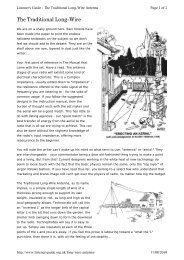
Aerials<br />
Apart from the two sets that are intended for use with an integral<br />
telescopic aerial, all the receivers described in this book are designed for<br />
use with a longwite aerial. Such an aerial is merely an insulated wire<br />
that is as long as can be accommodated and positioned as high up as<br />
possible. <strong>The</strong> aerial should preferably be set up well clear of buildings<br />
or other large obstructions. It should also be well insulated from the<br />
ground as otherwise some of the signals generated in it will be drained<br />
away straight to earth, rather than to earth through the receiver’s input<br />
coil. A typical method of fixing a longwire aerial is shown in Fig.2.<br />
11
Ideally the aerial should be some 20 to 40 Metres long overall<br />
(I.e. including the lead in wire), but as little as 10 Metres will suffice<br />
quite well. Generally speaking the longer the aerial the greater the signal<br />
It will provide. Thus when conditions are somewhat mediocre along<br />
aerial will provide a usable signal where a fairly short aerial will not.<br />
If 7/22 s.w.g. aerial wire can be obtained this is the best wire to<br />
use in the construction of the aerial. Ordinary 16 s.w.g. enamelled<br />
copper wire will also provide good results.<br />
An indoor aerial, mounted in a loft for instance, will give<br />
reasonably good results if it is at least 6 Metres long. An aerial any<br />
shorter than this will almost cettainly give poor results except when<br />
propagation conditions are exceptionally good.<br />
It is perhaps worth mentioning that for reception on the L.F.<br />
bands (either the amateur or commercial broadcast ones) the use of a<br />
long aerial of greater importance than it is on the H.F. bands. This<br />
is not to say that a fairly short aerial will, not give reasonable results on<br />
the L.F. bands, but merely that anyone who settles for such an aerial<br />
will be at more of a disadvantage on the L.F. bands than on the H.F.<br />
ones when compared to someone who has a long outdoor aerial. Anyone<br />
who is interested in DX reception on the L.F. bands should, of<br />
course, consider a proper outdoor antenna an essential.<br />
It is possible to use an aerial that has been designed to optimise<br />
performance on the band or bands that are of primary importance to<br />
the operator. However, this is a rather complicated subject, and it is<br />
probably better to use a longwire aerial initially. This is probably the<br />
most popular type of S.W. receiving aerial anyway, and is usualiy the<br />
most practical.<br />
Earth<br />
In contrast to a good aerial, and contrary to popular belief, an<br />
earth connection is by no means essential. It is not likely to be of much<br />
benefit to reception on the higher frequency bands, and in fact in most<br />
cases it will be of no help whatever.<br />
On the L.F. bands the situation is somewhat different. Here the<br />
use of an earth connection will normally provide a very noticeable<br />
and worthwhile increase in the strength of received signals. Even on<br />
the L.F. bands an earth is far from being a necessity, but is certainly<br />
worth adding where it can be accommodated without too much bother.<br />
It is an easy matter to construct an earth connection from a<br />
metal pipe, or any other piece of metal that has a fairly large surface<br />
area. <strong>The</strong> larger this surface area the more effective the earth should<br />
12
e. A length of wire is connected to the piece of metal which is then<br />
burriedt in any convenient patch of soil. <strong>The</strong> earth willbe more efficient<br />
if the soil is fairly moist and the metal pipe (or whatever) is made from<br />
a non-corrosive metal. Also make the lead-in wire to the receiver as<br />
short as possible in order to obtain optimum results.<br />
<strong>The</strong> general arrangement of a simple earth Is shown in Fig.3.<br />
13
Blank page<br />
14
Crystal Set<br />
CHAPTER 2<br />
Ultra Simple <strong>Receivers</strong><br />
A good starting point for anyone interested in building receivers<br />
is to build a crystal set. <strong>The</strong> main advantage of this type of set is its<br />
extreme simplicity. Another very important one is that they require<br />
no power supply and have no running costs. This tends to give crystal<br />
sets an added fascination over other types of receiver as it is actually<br />
the power of the received transmission that provides the energy that<br />
drives the diaphragm of the headphones or earpiece. It may seem<br />
impossible that the energy radiated from a transmitter some hundreds<br />
or even thousands of miles away can provide sufficient power to<br />
produce an acceptable volume at the transducer of the receiver, but<br />
indeed it can.<br />
Before considering a practical crystal set circuit it is a good idea<br />
to look at what the received signal is actually like.<br />
High frequency A.C. signals at the transmitter are radiated as a<br />
form of electro-magnetic signal which is usually termed radio waves.<br />
<strong>The</strong>se travel out from the transmitter at the speed of light (186,000<br />
miles per second) and when they reach a receiving aerial they generate<br />
minute electrical signals in that aerial. <strong>The</strong>se signals are identical to the<br />
original high frequency A.C. signal produced at the transmitter, but are<br />
of course at a very much lower power level.<br />
15
<strong>The</strong> signal can be considered as consisting of two parts, the<br />
carrier wave and the modulating signal. <strong>The</strong> carrier wave is the high<br />
frequency signal that carries the audio signal modulated onto it<br />
between the transmitting and receiving aerials, and it is from this that<br />
it derives its name. Fig.4 shows how the audio signal is amplitude<br />
modulated onto a carrier wave. Amplitude modulation (A.M.) is the<br />
form of modulation used by all commercial broadcast stations on the<br />
Long, Medium and Short Wave Bands.<br />
<strong>The</strong> receiver must carry out several basic functions in order to<br />
produce an audio output from a radio signaL <strong>The</strong>se basic requirements<br />
are shown in block diagram form in Fig.5. <strong>The</strong> first thing that the<br />
receiver must accomplish is to sort out the desired signal from the<br />
many thousands picked up by the aerial. As each of these signals will<br />
be on a different frequency the input circuitry of the receiver must be<br />
designed to respond to only a very narrow range of frequencies with all<br />
others being rejected. This ability is termed selectivity.<br />
<strong>The</strong> second function is that of detection, and this merely consists<br />
of removing one or other of the sets of half cycles of the signal, as<br />
shown in the diagram. <strong>The</strong> carrier signal provides no useful function<br />
beyond the detection stage, and is therefore filtered out. This leaves<br />
the final stage of the receiver which is the transducer. <strong>The</strong> purpose of<br />
this is to convert the audio frequency electrical signals into sound waves.<br />
17
Components List for Fig.6<br />
T1 Denco Green Range 4 Dual Purpose Coil.<br />
VC1 365pf air spaced (Jackson type ‘0’).<br />
Dl OA90 or OA9l.<br />
R1 100k ¼ watt 10%.<br />
High impedance headphones or earpiece. Control knob.<br />
Two wander sockets, one 3.5m.m. jack socket.<br />
Aluminium, B9A valveholder, wire, etc.<br />
Practical Circuit<br />
Fig.6 shows the circuit diagram of a practical crystal set. <strong>The</strong><br />
areial is coupled to the primary of R.F. transformer T1, and this causes<br />
to be induced into the secondary winding. This secondary winding,<br />
together with VC1, forms a tuned circuit. This type of circuit<br />
exhibits a high impedance at ‘resonance’, but this impedance falls to a<br />
low level above and below the resonant frequency. Thus only signals at<br />
or close to the resonant frequency will be permitted to pass on to<br />
subsequent stages, and all others will be shorted to earth through the<br />
tuned circuit. This part of the circuit therefore provides the frequency<br />
discriminating part of the unit. Adjusting VC1 allows the resonant<br />
frequency of the tuned circuit to be varied over a wide range of<br />
frequencies, and this is in fact an ordinary tuning control.<br />
Diode D1 acts as the detector, and a diode is a simple semiconductor<br />
which has the property of allowing a current to flow through it<br />
in one direction only. It is a sort of electronic valve. With D1 connected<br />
with the polarity shown in the diagram only the positive going half cycles<br />
are able to pass, and the negative going ones are blocked. In actual fact<br />
it does not matter which polarity of the signal is allowed to pass and<br />
which is blocked, and the circuit will function properly with Dl<br />
connected either way round.<br />
<strong>The</strong> transducer for the receiver is a pair of crystal headphones or<br />
a crystal earpiece. Some capacitance is required across the output to<br />
smooth the carrier signal to a D.C., and the self capacitance of the<br />
headphones is sufficient for this purpose. <strong>The</strong>re is no need to block<br />
this D.C. signal from the phones as it is too small to have an adverse<br />
effect on the circuit.<br />
<strong>For</strong> all practical purposes the resistance across a pair of crystal<br />
headphones can be regarded as being infinite. This can prevent the<br />
circuit from operating properly as the capacitance across the output<br />
can charge up to the peak level of the signal fed to it. and then of<br />
course the required audio signal is not produced across the headphones<br />
R1 is a bleeder resistor and this prevents such a charge from building up<br />
by providing a D.C. path across the output.<br />
18
It is also possible to use the circuit with a pair of high impedance<br />
magnetic (sometimes called moving coil) headphones. <strong>The</strong>se must be<br />
high impedance (4,000 ohms or more) phones or satisfactory results<br />
will not be obtained. <strong>The</strong>se do provide a D.C. path across the output<br />
and R1 can be omitted if magnetic headphones are used. As far as<br />
results are concerned, in the authors experience crystal and magnetic<br />
headphones provide about the same volume level, and either will work<br />
well. A crystal earphone (or two connected in parallel) is a cheaper<br />
alternative, but some of these are not very sensitive and could give<br />
disappointing results.<br />
When signals seem to be low in strength, or if a short aerial is<br />
being used, the alternative aerial connection point at SK2 can be used.<br />
This will provide a greater output volume, but this will be at the expense<br />
of selectivity. This will be discussed more fully later.<br />
An earth can be used with the receiver and can be plugged into<br />
SK3. Using an earth will not greatly improve performance, but bearing<br />
in mind that a really strong signal is needed to provide an audible output<br />
from the set, one must strive to obtain the strongest possible input<br />
signal for the set. It is therefore worthwhile using an earth if possible<br />
Coil Units<br />
As is the case with all the receiver circuits described in this book,<br />
the coils used are all ready made. Ready made coil units have the<br />
advantage of being made to very close tolerances and this gives the<br />
circuits reliable and repeatable results. Home wound coils tend to be<br />
far less consistant, and are not as easy for the amateur to wind us one<br />
might think. This tends to outweigh the economic advantage that<br />
home made coils have over the ready reade variety.<br />
<strong>The</strong> Denco coils specified cover the complete S.W. frequency<br />
spectrum in three ranges. <strong>The</strong>refore three coils are required to cover<br />
all the S.W. bands. <strong>The</strong> coils have nine pin bases which plug into a<br />
standard B9A valveholder. <strong>The</strong>re are two main reasons for using this<br />
arrangement. One is that the coils are wound on polystyrene formers<br />
which tend to melt if the pins are soldered to direct. Making the<br />
soldered joints to the holder avoids this problem.<br />
<strong>The</strong> other advantage is that this enables a very simple method<br />
of bandchanging to be used. <strong>The</strong> required band is selected by simply<br />
plugging in the appropriate coil. Admittedly this method is less<br />
convenient than using a wavechange switch, but it makes receiver<br />
construction very much more simple by considerable reducing the<br />
complexity of the wiring. It is also less expensive than employing<br />
a wavechange switch, and enables a neater and more compact<br />
receiver to be built as space for only one coil has to be found on the<br />
receiver’s chassis.<br />
19
To those unfamiliar with this method of band changing it may<br />
seem to be a little unusua1,but in fact, it is almost universaly used in<br />
simple S.W. receiver designs, and is even employed in a few highly<br />
sophisticated Sets. One thing it is, is very practical and this accounts<br />
for its widespread adoption, and its recommended use with the<br />
receiver circuits described here.<br />
When using the specified 365 pF tuning capacitor the three<br />
ranges have the approximate frequency coverage shown below: -<br />
Range 3 l.5 to 5.5 MHZ<br />
Range 4 5.0 to 17.0 MHZ<br />
Range 5 10.0 to 35.5 MHZ<br />
Note that these are only approximate, and the exact frequency<br />
coverage of a receiver is influenced to some extent by the tolerances<br />
of the components used and by stray capacitances present in the<br />
circuit. It is also affected, and to a far greater extent, by the setting<br />
of the adjustable core of each coil.<br />
Some readers may be confused by the fact that some receiver<br />
circuits shown in these pages use coils intended for valve circuits (the<br />
D.P. coils) and some use coils intended for transistor circuits (those<br />
that have a letter T after the range number), whereas all the designs<br />
are solid state ones. This is because many of the designs use field<br />
effect transistors (FETS) and these are very different to ordinary<br />
bipolar transistors. <strong>The</strong> primary difference is that FETs haye<br />
extremely high input impedances and so do valves, but dipolat transistors<br />
havecomparatively low input impedances. Thus coils that are intended<br />
for valved circuits can be easily and well adapted to FET circuits, whereas<br />
coils that are intended for bipolar transistor circuits cannot.<br />
<strong>The</strong> crystal set is really only designed to operate with a Range 4<br />
coil, and this has the 49, 41, 31, 25 and 19 Metre broadcast bands within<br />
its coverage. <strong>The</strong>se provide the most prolific selection of stations when<br />
using a very simple set such as this.<br />
It is possible to use the Range 3 and Range 5 coils, and the set<br />
will function just as well on these ranges, but good results are not likely<br />
to be obtained as there are not such a large number of stations providing<br />
suitable signals on these ranges. Reception of the ordinary M.W. broadcast<br />
band can be provided by using a Range 2 coil.<br />
A crystal set is not really suitable for amateur band reception as<br />
amateur transmitters are restricted to a relatively low output power,<br />
and this means that few, if any, signals of sufficient strength can be<br />
received on these bands. Anyway, these days the majority of amateurs<br />
use modes of transmission that cannot be resolved by a crystal set even<br />
if a signal of adequate strengtl is received.<br />
20
Construction<br />
<strong>The</strong> crystal set can be inexpensively constructed on a home made<br />
chassis and panel having the dimensions shown in Fig.7. This also gives<br />
details of the drilling and folding of the chassis and panel. <strong>The</strong>y are<br />
constructed from aluminium, and a relatively thin gauge, say about<br />
20 s.w.g. will provide a structure of adequate rigidity and strength. A<br />
thicker gauge could be used, but would be more difficult to work and<br />
fold.<br />
3 or 4 mm wander sockets are the most suitable type to use for<br />
the aerial and earth sockets, and a 3.5 mm jack socket makes a suitable<br />
outlet to the headphones.<br />
<strong>The</strong> ¾ in. diameter cutout for the B9A coilholder is made using a<br />
chassis punch. If a suitable punch is not available, it is possible to cut<br />
this using a miniature round file or a fretsaw fitted with a fine toothed<br />
blade.<br />
If the specified Jackson type ‘0’ tuning capacitor is used, a total<br />
of four mounting holes will be required for this component. A central<br />
0.375 in. (10 mm) diameter hole is required for its spindle and three 4BA<br />
clearance holes are required fot the mounting bolts. <strong>The</strong>se are short<br />
4BA countersunk types and, incidentally, these are not usually supplied<br />
with the capacitor.<br />
Probably the easiest method of locating the positions of the<br />
three small mounting holes is to make a paper template. To do this<br />
simply take a small piece of paper (about 40 to 50 mm square) and<br />
make a 7 mm diameter hole in its centre. <strong>The</strong>n thread this over the<br />
spindle of the tuning capacitor and press it up against the front plate<br />
of this component. It should then be possible to punch three holes in<br />
the paper with the point of a pencil above the positions of the three<br />
holes in the capacitors front plate. This completes the template.<br />
<strong>The</strong> three mounting bolts pass through the panel and into the<br />
threaded screw holes in the front of VC1, but a few words of warning<br />
are in order here. <strong>The</strong> mounting bolts must not be allowed to protrude<br />
more than 1 or 2 mm through the front plate of VC1. If they should<br />
do so they may well come into contact with one of the capacitors sets<br />
of vanes and this could jam the unit, or in extreme cases it could<br />
possibly even irreparably damage the capacitor.<br />
It is unlikely that the constructor will be able to obtain suitably<br />
short mounting bolts, and it will almost certainly be necessary to use<br />
spacers over these bolts, between the front plate of VC1 and the front<br />
panel of the receiver, in order to reduce the penetration of the screws<br />
to an acceptable level. Some 4BA washers or three 2BA nuts are<br />
usually sufficient for this purpose.<br />
22
<strong>The</strong> completed chassis and panel are held together using a couple<br />
of 4BA nuts and bolts.<br />
Wiring<br />
<strong>The</strong>re are very few connections to be made in this simple<br />
receiver, and a straight forward point to point wiring system is the most<br />
practical method of wiring up the set. A complete wiring diagram of<br />
the unit is shown in Fig.8.<br />
Modern components have leads that do not easily oxidize as they<br />
have been developed for modern automatic production methods. This<br />
simplifies soldering and it is not necessary to clean the component lead<br />
out wires unless they are obviously very heavily oxidized. Once the<br />
component leads have been cut to length their ends should be tinned<br />
with solder, and the tags of sockets, etc. should be similarly tinned<br />
before attempting to complete a soldered joint. Use a multi-core solder<br />
and use plenty of solder on each joint. Try not to move the components<br />
while they are being connected. Keep to these guide lines and<br />
good soldered joints should be obtained.<br />
23
Do not keep the iron on any joint any longer than is absolutely<br />
necessary. All components can be damaged by excessive heath and<br />
semiconductor devices are especially vulnerable. Germanium devices<br />
such as diode D1 are very easily harmed by excessive heat, and it is<br />
adviseble to use a heatshunt on each lead as it is connected. Heatshunts<br />
are available, but it is not real ly necessary to use a proper headshunt,<br />
and gripping the wire with a pair of long nose pliers, between the body<br />
of the component and the joint, should be equally effective.<br />
Note that the earth connections to VC1 and SK3 are made via<br />
the chassis, and for this reason only one lead connects to each. SK3<br />
must obviously be an ordinary jack socket of the open construction<br />
variety, and not an insulated type. Conversely, the aerial and earth<br />
sockets should be of an insulated1type as otherwise the aerial connections<br />
will be shorted to earth. This obviously would not matter in the case<br />
of the earth socket which is connected to the chassis anyway, but for the<br />
sake of a neat appearance this socket should match the aerial ones.<br />
<strong>The</strong> Denco coils are supplied in an aluminium container which<br />
can be used as a screening can. Screening of the coils is not necessary<br />
in any of the simple designs described here, and these cans are discarded.<br />
<strong>The</strong> adjustable core of each coil is always screwed right down when the<br />
coils are received, so that they will fit into their containers. <strong>The</strong> cores<br />
should be unscrewed slightly so that about 5 to 10 mm of screwthread<br />
protrudes from the top of each coil. This applies to all the circuits<br />
described in this book, and not just to the crystal set.<br />
If a suitable signal generator is available it is possible to adjust<br />
the cores to give the correct frequency coverage on each band. However,<br />
as it is unlikely that the majority of readers will have access ft<br />
such equipment, such precise setting up is not really feasible.<br />
<strong>For</strong>tunately it is not really necessary anyway, and even if the<br />
adjustment of the cores is considerably out, the frequency coverage<br />
will not be so seriously affected that any of the broadcast or amateur<br />
bands will be lost from any receiver’s coverage. Neither will there be<br />
any gaps in the coverage of multiband receivers as there is a considerable<br />
overlap in the coverage of each coil range. Also, the upper and lower<br />
limits of the coverage obtained with the coils and the specified tuning<br />
capacitor, extend well aboye and below the limits of the S.W. frequency<br />
spectrum. <strong>The</strong>refore, in the circuits described here anyway, the settings<br />
of the cores should not be considered too critical.<br />
Using the Set<br />
Operating the cryrtal set is really very straightforward. <strong>The</strong>re is<br />
only one control and that is a conventional tuning control the tuning<br />
will be fairly broad and if must ho admitted that the selectivity of a<br />
24
crystal set is not very high. This particularly so when the aerial is<br />
plugged into SK2, as the aerial then has a strong loading effect on the<br />
tuned circuit; and its efficiency is severely reduced. Thus even though<br />
stronger signals will be produced by plugging the aerial into SK2, and<br />
there is a strong temptation to simply ignore SK1, the greater selectivity<br />
obtained with the aerial connected to SK1 makes this the better of the<br />
two most of the time. Only use SK2 when conditions are such that<br />
only very weak signals are obtained when using SK1.<br />
A degree of patience is required in order to obtain good results<br />
from any S.W. Receiver, but this is especially so in the case of a S.W.<br />
set. Stations temporarily fading out completely is one problem, and<br />
another is that one station on the band can suddenly become exceptionally<br />
strong, and blot out reception of the desired transmission, eventhough<br />
it is at a good strength.<br />
Despite its deficiencies, a lot of fun can be had from a crystal<br />
set, and stations some thousands of miles away can be received if one<br />
perseveres.<br />
Regenerative Receiver<br />
Unlike the crystal set, most receivers have a large amount of gain.<br />
This enables very weak signals to be boosted to a level that produces a<br />
good level of volume from the transducer. It also enables the selectivity<br />
of the receiver to be greatly improved, and this is just as important as<br />
the increased sensitivity.<br />
One of the most widely used types of detector in simple S.W.<br />
receivers is the regenerative detector. Basically this just consists of a<br />
transistor (or other active device) in one of its normal amplifying modes.<br />
A capacitor is connected across the output, as it is in the case of a diode<br />
detector, to remove the R.F. content at the output of the detector.<br />
It may not be immediately obvious how this arrangement<br />
provides rectification, and in fact this type of detector may seem to be<br />
a little unusual to those who are not familiar with the technique<br />
employed. It relies upon the fact that no contemporary amplifying<br />
devices are completely linear in operation, and the gain of an ordinary<br />
transistor for instance, tends to rise with increasing collector ciurrent.<br />
If it Is used to amplify an R.F. signal it will therefore tend to<br />
amplify one set of half cycles more than the other set. It will amplify -<br />
the positive input half cycles more than the negative ones. This provides<br />
a very crude and inefficient form of rectification, and of course, it is<br />
rectification that the detector must provide.<br />
Regeneration is applied to the circuit in order to greatly increase<br />
the detection efficiency of the circuit. Regeneration is merely positive<br />
feedback or sending some of the signal bock from the output to the<br />
25
input of the circuit so that it is amplified for a second time. This is<br />
sometimes given its alternative term, ‘reaction’.<br />
One effect of regeneration is to increase the gain of the circuit,<br />
but the important feature is that it will not increase it by an equal<br />
amount on all signals, or even on all parts of each signal.<br />
<strong>For</strong> instance, the positive input half cycles are at a greater<br />
amplitude at the output than are the negative ones, and therefore a<br />
larger amount of feedback is produced on the positive input half cycles.<br />
This causes a larger increase in gain on the positive input half cycles than<br />
on the negative ones, and regeneration thus increases the detection<br />
efficiency of the circuit. This is illustrated in Fig.9 which shows the<br />
input, output, and output after regeneration waveforms of typical<br />
regenerative detector, with an unmodulated R.F. input.<br />
A regenerative detector has a considerable level of gain, and it<br />
is far more sensitive than a simple diode detector of the type used in<br />
the crystal set.<br />
Increased Selectivity<br />
Using regeneration also greatly boosts the selectivity of a receiver.<br />
If a graph showing frequency versus sensitivity for a crystal set was plot-<br />
26
ted it would look something like the graph shown in Fig.10(a). <strong>The</strong> peak<br />
occurs at the resonant frequency of the tuned circuit, and the response<br />
only falls away gradually either side qf this. As a result, the receiver has<br />
only a very limited degree of selectivity, and when a transmission is<br />
present within a few tens of KHZ of the desired one, both signals will<br />
fall within the receiver’s passband, and it will not be possible to tune to<br />
only one or other of them.<br />
Regeneration will boost signals at or near the centre of the<br />
receiver’s response by a far larger amount than it will boost signals<br />
towards the edges of the response. It does this in just the same way as it<br />
boosted positive input signals more than negative ones. This gives the<br />
receiver a passband something like that shown in Fig.10(b). <strong>The</strong> ‘bandwidth’<br />
as it is termed, is greatly reduced, and the receiver is capable of<br />
accepting only one of two closely spaced signals.<br />
This feature is very important for any S.W. receiver, because a<br />
large number of S.W. stations tend to be crammed into each band, and a<br />
sensitive receiver with poor selectivity would simply receive a jumble<br />
of signals and would not be able to produce a coherent output.<br />
27
Components List for Fig.11<br />
Resistors, all ¼ watt 10%.<br />
R1 18k R4 680 ohms.<br />
R2 3.3k R5 2.2 Meg.<br />
R3 1.8k R6 5.6k.<br />
VR1 10k linn. carbon.<br />
Capacitors.<br />
C1 100mfd. l0v.w.<br />
C2 6.8nf polystyrene.<br />
C3 10nf plastic foil or ceramic.<br />
C4 5.6nf polystyrene.<br />
C5 4mfd. 10v.w.<br />
C6 100nf plastic foil.<br />
VC1 365pf air spaced (Jackson Type ‘0’).<br />
VC2 50pf air spaced (Jackson Type C804).<br />
Semiconductors.<br />
Tr1 BF115.<br />
Tr2 BC109.<br />
Inductor.<br />
T1 Denco Transistor Useage coils Ranges 3T, 4T, and 5T, Yellow.<br />
Switch.<br />
S1 S.P.S.T. toggle switch.<br />
Miscellaneous.<br />
B9A valveholder, PP3 battery and clips to suit.<br />
Two wander sockets and one 3.5m.m. jack socket.<br />
Aluminium, control knobs, wire, etc.<br />
Circuit Operation<br />
<strong>The</strong> circuit diagram of the regenerative receiver appears in Fig.11.<br />
Looking at this in very broad terms, Tr1 is the regenerative detector and<br />
Tr2 is a high gain audio amplifier.<br />
Tr1 is used in the common base mode and is biased by R1 and<br />
VR1. C3 couples Tr1 base to earth at R.F. <strong>The</strong> tuned winding of T1<br />
provides the R.F. collector load for Tr1, and VC1 is the tuning capacitor.<br />
<strong>The</strong> collector and emitter of Tr1 are in phase, and so in order to provide<br />
the required positive feedback it is only necessary to couple these two<br />
points by way of a variable capacitor. This is VC2 and it is the regeneration<br />
control. VR1 also acts as a sort of regeneration control, and the use<br />
of these two controls will be fully dealt with later.<br />
<strong>The</strong> aerial signal is coupled to the detector via the primary<br />
winding of T1. <strong>The</strong> audio output is developed across R2 and C2 is the<br />
R.F. filter capacitor. C6 provides D.C. blocking between the detector<br />
and audio stages of the receiver.<br />
This capacitor may seem to have rather a low value for the<br />
impedance into which it is working. By the standards of entertainment<br />
29
eceivers it does have too low a value, but in entertainment equipment<br />
one is aiming for the widest possible frequency response, ‘whereas in<br />
communications equipment the aim is to obtain a signal that has the<br />
highest possible intelligibility. <strong>The</strong> low value of C6 produces a considerable<br />
attenuation of bass and low middle frequencies, but this actually<br />
makes received signals easier to understand.<br />
It is also an advantage to roll off the upper audio frequencies<br />
above about 2.5 to 3.5 kHZ, as this not only increases the intelligibility<br />
of the signal, but it also greatly reduces the background noise level.<br />
R4 and C4 form a simple low pass filter which fulfils this requirement.<br />
This network also provides additional R.F. filtering. It is absolutely<br />
essential to ensure that no R.F. signal finds its way into the audio<br />
circuitry, as an audio amplifier employing a silicon transistor has a<br />
frequency response that extends well into the S.W. frequency spectrum,<br />
and even beyond this into the V.H.F. range. Silicon transistors can<br />
provide high gains and low noise levels, and large use is made of them<br />
in the audio stages of the receivers described here.<br />
<strong>The</strong>re are two main problems that are likely to result from<br />
insufficient R.F. filtering. One, and usually the lesser of the two, is<br />
the breakthrough of unwanted signals, and these signals are often well<br />
away from the actual band being tuned in terms of frequency. <strong>The</strong>y<br />
are actually picked up in the wiring at the input to the audio amplifier,<br />
and not by the aerial.<br />
<strong>The</strong> second problem, and by far the most troublesome, is that of<br />
the signal being greatly amplified by the audio amplifier, and then fed<br />
back to the R.F. section of the circuit through stray circuit capacitances<br />
This can manifest itself in either of two ways. If the stray feedback is<br />
positive, the circuit will oscillate uncontrollably and proper reception<br />
will not be possible. If the feedback is mainly negative it will severely<br />
reduce the sensitivity of the receiver, and could render the regeneration<br />
control almost totally ineffective.<br />
Efficient and effective R.F. filtering is therefore absolutely<br />
essential with this type of receiver, and very simple methods of the<br />
type used with the crystal set are simply not good enough.<br />
<strong>The</strong> gudio stage of the receiver Is a conventional high gain<br />
common emitter amplifier using an inexpensive BC109 transistor or<br />
one of its many equivalents. R6 is the collector load resistor and R5<br />
is the base bias resistor. R5 introduces a certain amount of negative<br />
feedback over the audio amplifier and this does reduce the, gain of the<br />
stage by a small degree. However, it is still a good idea to use this<br />
method as the feedback gives avery stable biasing system that only<br />
requires a single resistor. Also, the use of some negative feedback<br />
gives improved quality to the audio output.<br />
30
<strong>The</strong> slight loss of gain is not really important since the circuit<br />
still has more than adequate output to drive virtually any medium to<br />
high impedance headphones. <strong>The</strong> audio output is fed to the output<br />
socket via D.C. blocklng capacitor C5.<br />
Cl is a supply decoupling capacitor and is required in order to<br />
prevent feedback between the two amplifying stages through the<br />
supply lines. S1 is an ordinary on/off switch.<br />
As the set consumes only about 2.5 to 3 mA from a 9 volt<br />
supply, a small battery such as a PP3 will provide very economical<br />
operation of the receiver. In fact even with frequent use, the battery<br />
will probably have virtually its shelf life.<br />
Transistors<br />
<strong>The</strong> BC109 transistor sometimes has a letter added at the end of<br />
its type number (e.g. BC109B). This is the gain grouping of the transistor,<br />
and there are three groups for most audio transistors. Group ‘A’ is the<br />
lowest gain, group ‘B’ is the medium gain one, and group ‘C’ is the<br />
highest gain grouping. <strong>The</strong> BC109 being a high gain device is only<br />
avai1able with a B or a C suffix.<br />
Any BC109 can be used in this circuit, or any of the circuits in<br />
this book where a BC109 is specified, and whether it his a B or a C<br />
suffix, or none at all, the level of performance will not be significantly<br />
affected.<br />
<strong>The</strong> BF115 transistor is a little unusual in that it has four leadouts<br />
rather than the usual three. <strong>The</strong> additional leadout wire is a shield (s)<br />
connection, and this merely connects to the metal case of the device.<br />
Usually this lead is connected to earth, but in this circuit it is<br />
simply ignored.<br />
Construction<br />
<strong>The</strong> receiver can be conveniently constructed on a chassis add<br />
panel of the same basic type as those used for the crystal set. In order<br />
to obtain sufficient space for all the components without undue crowding<br />
they really need to be somewhat larger. A 152 x 102 x 63 mm<br />
chassis and a 152 x 102 mm panel should be adequate. Suitable ready<br />
made 18 s.w.g. aluminium chassis are available if the constructor does<br />
not wish to build his or her own.<br />
It is probably better to use an S.R.B.P. panel (or one made from<br />
a similar insulative material) rather than use an aluminium one. This is<br />
because the moving yanes of VC2 are In electrical contact with the<br />
components mounting bush. Mounting VC2 on a metal panel causes it<br />
31
to have on. connection earthed. In most circuits the variable capacitors<br />
have one set of vanes connected to earth anyway, and so this is usually<br />
an advantage as it saves having to use a lead to earth one side of each<br />
variable capacitor.<br />
VC2 of this circuit is an exception though, and neither of its<br />
connections should connect to earth. <strong>The</strong>refore, if a metal panel is used,<br />
some way of mounting VC2 without it being electrically connected to<br />
the panel must be found.<br />
In all the other circuits in this book each variable capacitor has<br />
one connection earthed, and so this problem does not arise.<br />
Much of what was stated earlier about the mechanical construction<br />
of the crystal set also applies to the regenerative receiver, and will<br />
not be repeated.<br />
A complete wiring diagram of the receiver is shown in Fig.12.<br />
In this it has, been assumed that both VC1 and VC2 are mounted above<br />
chassis and that a front panel made from an insulative material has been<br />
used.<br />
A simple point to point wiring system is used in the construction<br />
of the detector circuitry, and again, what was stated earlier about wiring<br />
up the crystal set also pertains to this wiring, and will not be repeated.<br />
<strong>The</strong> A.F. circuitry is constructed on a 0.15 in. pitch Veroboard<br />
which has 11 x 12 holes. <strong>The</strong> copper strips run across the width of<br />
the panel. <strong>The</strong> board is not sold in pieces of this size, and the panel must<br />
be carefully cut down from a larger piece using a hacksaw. <strong>The</strong> mounting<br />
holes can be drilled for either 6BA mounting bolts (No.31 twist drill) or<br />
for metric M3 mounting bolts (3.3 mm diameter twist drill).<br />
Soldering components onto a Veroboard panel is easier than the<br />
point to point wiring. Good soldered joints should result provided<br />
plenty of solder is used on each joint, and the leadout wires are cut to<br />
length before they are connected. Cutting them to length afterwards<br />
could break the copper strips away from the backing material, and will<br />
not give such a neat finish. Incidentally, there are no breaks in any of<br />
the copper backing strips with this particular design.<br />
Always leave semiconductor devices until last when wiring up a<br />
Veroboard, or any panel of a similar type for that matter. This reduces<br />
the risk of damaging any of the semiconductors through overheating.<br />
Make sure that all electro1ytic capacitors are connected with the correct<br />
polarity. <strong>The</strong> polarity is usually marked on the body of the component,<br />
or the positive (+) connection is indicateclby an indentation around the<br />
body of the capacitor towards the appropriate end of the component.<br />
32
Wire the completed Veroboard panel to the rest of the circuit<br />
using ordinary multistand P.V.C. insulated connecting, and then mount<br />
it on the underside of the chassis. Some spacers or extra nuts must be<br />
used to space the panel well clear of the metal chassis, as otherwise the<br />
connections on the reverse side of the panel will be short circuited<br />
through the chassis.<br />
Using the Receiver<br />
This receiver is primarily intended for use on the broadcast<br />
bands using the Range 4T and 5T coils. It will not work very efficiently<br />
using a Range 3T coil, except towards the high frequency end of the<br />
band where a number of stations on the 60 Metre broadcast band can<br />
be received.<br />
<strong>The</strong> tuning on on/off controls are quite conventional, but the<br />
reaction controls are not volume controls, and they require very careful<br />
adjustment if really good results are to be obtained from the<br />
receiver.<br />
<strong>The</strong> detector will operate most efficiently with VR1 turned well<br />
back (i.e. adjusted almost fully anticlockwise), as it is then that the<br />
difference in the levels of amplification given to each set of half cycles<br />
is most unequal. <strong>The</strong>refore VR1 should be kept well backed off and<br />
VC2 is advanced to just below the threshold of oscillation. It should<br />
perhaps be explained that by advancing VC2, it is meant that the two<br />
sets of vanes should be more fully meshed together.<br />
It is with the detector set just below the threshold of oscillation<br />
that the set has the highest degree of sensitivity and selectivity. Adjusting<br />
VC2 too far will result in the receiver breaking into oscillation, and<br />
the practical result of this will be that a whistle of varying pitch will be<br />
heard as the receiver is tuned across a station, and proper reception will<br />
not be possible with the receiver in this condition.<br />
Fine adjustment of the reaction level is probably best carried<br />
out using VR1. This does not control the amount of feedback, but<br />
affects the gain of Tr1, and this permits it to be used as a reaction<br />
control. It will not provide anything like the degree of control that is<br />
available using VC2, but it is this that makes it so much better for<br />
making the fine adjustments of the regeneration level.<br />
Towards the low frequency end of each band (VC1 vanes well<br />
meshed) it will almost certainly be found that the detector cannot be<br />
brought to the threshold of oscillation with VR1 turned well back. It<br />
is then necessary to advance VR1 somewhat. This does reduce the<br />
detection efficiency of the set, but the gain of the detector is increased.<br />
This increased gain tends to compensate to some degree for the loss of<br />
efficiency, and good results should still be obtained.<br />
34
It is very worthwhile experimenting a little with the settings of<br />
the reaction controls to see which positions give the best results. Every<br />
time the setting of the tuning control is significantly altered, some<br />
readjustment of the reaction controls will be required in order to maintain<br />
optimum working conditions of the detector. A fair amount of<br />
skill is required when using simple S.W. receivers, and it will probably<br />
be necessary to gain a certain amount of experience with the receiver<br />
before the operator learns how to get the most out of it. This applies<br />
to all simple S.W. sets.<br />
Simple Improvements<br />
It is possible to make one or two simple improvements to the<br />
basic receiver, and these improvements also apply to most of the other<br />
sets described in this book.<br />
Bandspread<br />
Although the crystal set covers a wide range of frequencies,<br />
tuning in a station accurately is quite simple as the set has a relatively<br />
wide bandwidth. <strong>The</strong> regenerative receiver has a very much more<br />
narrow bandwidth than the crystal set and a much higher sensitivity.<br />
This makes tuning much more difficult, as adjusting the tuning<br />
knob through only one or two degrees could tune the receiver over a<br />
dozen or more stations. Thus very careful adjustment of the tuning control<br />
is required in order to accurately tune to a station. Most people find<br />
tuning to a station with a reasonable amount of precision quite difficult<br />
on this type of set, and usually some form of bandspread is fitted<br />
to the receiver to make tuning easier.<br />
<strong>The</strong>re are two forms of bandspread, mechanical bandspread<br />
and electrical bandspread.<br />
Mechanical bandspread merely means fitting a slow motion<br />
drive to the tuning control. If, for instance, a six to one reduction<br />
drive is fitted, instead of only half a turn of the tuning knob being<br />
required to tune from one end of a tuning range to the other, three<br />
complete turns will be required. This makes tuning very much easier.<br />
Several commercially produced tuning reduction drives are available,<br />
and some have two reduction ratios, usually six to one and thirtysix<br />
to one. <strong>The</strong> higher reduction ratio is used for normal tuning, and the<br />
lower ratio enables the user to quickly tune from one end of the tuning<br />
range to the other without laborious turning of the tuning knob.<br />
Some drives are a combination of a tuning dial and a reduction<br />
drive. <strong>The</strong>se are excellent, although they are usually a little expensive.<br />
35
Electrical bandspread is an electrical equivalent of a mechanical<br />
reduction drive, and simply consists of adding a low value variable<br />
capacitor in parallel with the main tuning capacitor. This is shown in<br />
the circuit of Fig.13. <strong>The</strong> value of the additional capacitor is not critical,<br />
and can be anything from about 15 to 50 pF.<br />
In use the main tuning control, or ‘Bandset’ control as it is normally<br />
termed when a bandspread capacitor is fitted, is set to the band<br />
that is to be searched for transmissions. <strong>The</strong>n the actual tuning is<br />
accomplished using the bandspread control.<br />
As the bandspread capacitor has a much lower value than the<br />
bandset one, it only covers a very small part of each tuning range.<br />
Tuning is therefore far less cramped using the bandspread control.<br />
This type of electrical bandspread used to be the standard method<br />
used in simple receivers, but variable capacitors are relatively expensive<br />
these days, and mechanica1 or other electrical methods are now often<br />
employed instead.<br />
A special type of diode known as a variable capacitance diode<br />
(often abbreviated to varicap.) can be used as a cheaper alternative. This<br />
component has the property of changing its capacity in proportion to the<br />
level of reverse bias applied to it.<br />
What is happening is that the two pieces of silicon that form the<br />
diode are acting as the plates of the capacitor. <strong>The</strong> insulating layer that<br />
exists between the two pieces of silicon, and which is called the depletion<br />
36
layer, acts as the dielectric of the capacitor. <strong>The</strong> larger the reverse bias<br />
that is applied to the diode, the deeper the depletion layer becomes. This,<br />
in effect, increases the distance between the two plates of the capacitor,<br />
and causes a reduction in the capacity of the diode.<br />
<strong>The</strong> circuit shown in Fig.14 illustrates how a varicap. diode can be<br />
used as the basis of a simple bandspread control. <strong>The</strong> fixed capacitor<br />
provides D.C. blocking and prevents the voltage fed to the diode from<br />
being short circuited through the tuning coil. <strong>The</strong> tuning voltage set at<br />
the slider of the potentiometer must be fed to the varicap. diode via a<br />
high value resistor, so that the capacitance of the diode is shunted by a<br />
very high value of resistance. Since only minute leakage currents flow<br />
in the resistor, a significant voltage is not dropped across it despite its<br />
high value.<br />
Another simple method of adding bandspread is shown in Fig.15.<br />
<strong>The</strong> operation of this is very straightforward. <strong>The</strong> variable resistor<br />
virtually cuts the capacitor out of circuit when it is set for maximum<br />
resistance. When it is at minimum resistance the capacitor is shunted<br />
across the tuning capacitor. Intermediate settings of the variable resistor<br />
give intermediate levels of effective capacitance across the tuning capacitor,<br />
and the potentiometer thus acts as a simple bandspread control.<br />
While this method is much cheaper than the previous methods, it<br />
does have the disadvantage that it will only provide a relatively small<br />
tuning range. It cannot be used in quite the same way as the other two<br />
circuits, and it is best to use the main tuning control to roughly tune to<br />
the desired station, and then use the bandspread control for the fine<br />
tuning.<br />
37
Overloading<br />
Another problem with simple S.W. receivers is that of overloading<br />
on strong signals. When this happens there is usually a large amount of<br />
background noise from the headphones, and the set will have an apparent<br />
lack of selectivity.<br />
When this occurs it is necessary to reduce the strength of the aerial<br />
signal, and this can be accomplished using the simple attenuator circuit<br />
shown in Fig.16. SK1 is the normal aerial socket, and when overloading<br />
occurs the aerial is connected to SK2 instead. This introduces a low<br />
value fixed capacitor into circuit between the aerial and the input<br />
coupling coil of the receiver. Losses in the capacitor reduce the signal<br />
38
level that reaches the detector of the receiver, and so elliminate the overloading.<br />
<strong>The</strong> less tight coupling of the aerial to the tuned circuit increases<br />
the selectivity of the receiver slightly, and this also helps to remove the<br />
overloading.<br />
Cases<br />
If the constructor wishes to house any of the receivers described<br />
here in an outer casing, it is an easy matter to construct a case from<br />
plywood using ordinary glued butt joints. Self adhesive plastic material<br />
can be used to cover the completed case, and should provide a very<br />
attractive finish.<br />
One point must be borne in mind however. Unless the receivel<br />
is to be used on only one range, the lid of the cabinet must be easy to<br />
remove in order to facilitate coil changing. Another popular method<br />
is to use a hinged lid, or to have a hinged compartment in the lid<br />
above the coilholder.<br />
Construction Hints<br />
Fairly detailed constructional information has been provided for<br />
these first two receivers, and this should give the reader a good general<br />
idea of the methods used when building simple S.W. sets. <strong>The</strong> circuits<br />
shown in the remaining part of this book will be discussed in comparatively<br />
broad terms and constructional information will not be provided.<br />
Provided a few points are kept in mind, little difficulty should<br />
arise when translating a circuit diagram into a practical design.<br />
It is important that all wiring that carries R.F. should be kept as<br />
short and direct as possible. This is particularly important in the case<br />
of R.F. decoupling capacitors. <strong>For</strong> this reason it is advisable to use<br />
point to point wiring in the R.F. and detector circuitry.<br />
Avoid having R.F. chokes, tuning coils, and even speaker coils<br />
very close to one another. Feedback between two closely spaced coils<br />
can upset the operation of the circuit.<br />
Wiring of the audio circuitry of a receiver is not usually too<br />
critical, and Veroboard, plain matrix boards, tagstrips, etc. are suitable<br />
for use here. However, try to keep input and output leads well away<br />
from one another, particularly where two stages of audio amplification<br />
are used. It is also a good idea to keep the wiring at the input of the<br />
audio stages as short as possible so that there is a minimum of stray<br />
pick-up of mains hum, and similar A.F. interference.<br />
39
One final point is that with S.W. receiver designs it is not a good<br />
idea to deviate from the specified component values. <strong>The</strong>se tend to be<br />
a little more critical than with other types of equipment and even if<br />
changing a component value does not prevent a receiver from working<br />
all together, it may well result in a loss of performance.<br />
40
CHAPTER 3<br />
General Purpose <strong>Receivers</strong><br />
In this chapter a number of general purpose S.W. receiver designs<br />
will be described. <strong>The</strong>se will all give good results on both the amateur<br />
and broadcast bands. Some of the circuits are extremely simple and<br />
inexpensive to construct, and others are a little more sophisticated. In<br />
general, and as one would expect, the more complex designs offer the<br />
best performance and greater flexibility in use, but even the more simple<br />
designs will provide excellent results.<br />
Regenerative FET Receiver (Fig.17)<br />
Field effect transistors (FETs) have several advantages over<br />
ordinary bipolar transistors in the stages of a S.W. that handle R.F.<br />
signals. <strong>The</strong>re are two basic types of FET, Junction Gate FETs, and<br />
Metal Oxide Silicon FETs. <strong>The</strong>se names are usually abbreviated to<br />
JUGFET and MOSFET respectively. Most MOSFETs currently in use<br />
have two gates, and are called Dual Gate MOSFETs. Any of these<br />
devices will work well in simple S.W. receiver designs, provided of<br />
course, that they are intended for use at high frequencies. In the<br />
present design a JUGFET is used, and this is the widely available<br />
and inexpensive 2N3819 device.<br />
<strong>The</strong> complete circuit diagram of the ‘Regenerative FET Receiver’<br />
is shown in Fig.17, and as will be seen from this, apart from the FET,<br />
only one other active device is used. This is a 748C operational amplifier<br />
which is used here as a high gain audio amplifier.<br />
If we consider this circuit in greater detail, the aerial signal couples<br />
to the primary winding of T1, and the secondary winding of T1 together<br />
with VC2 forms the tuned circuit. VC2 is the normal tuning capacitor.<br />
<strong>The</strong> signals induced into the tuned circuit are coupled direct into the gate<br />
of Tr1. An FET has three terminals, and these are termed the gate, drain<br />
and source. <strong>The</strong>se are the equivalents of the base, collector and emitter,<br />
respectively, of a bipolar transistor.<br />
<strong>The</strong> direct coupling to the gate of Tr1 will seem a little unusual<br />
to those who are unfamiliar with FETs. Unlike a bipolar device, a FET<br />
has quite a low resistance between its drain and source terminals with no<br />
bias applied to its gate. Whereas an ordinary transistor must be forward<br />
biased before it can be used as a practical amplifier, a FET must be<br />
reverse biased. This is achieved by using source resistor R2 and holding<br />
the gate at chassis potential. Usually a resistor is used to tie the gate to<br />
chassis, but in this case the tuned winding of T1 performs this task.<br />
41
Components List for Fig.17<br />
Resistors (¼ watt 5%).<br />
R1 1k R5 39k<br />
R2 680 ohms R6 100k<br />
R3 2.2k R1 100k<br />
R4 39k R8 1k<br />
Capacitors.<br />
C1 10nf plastic foil or ceramic.<br />
C2 100mfd. 10v.w.<br />
C3 15nf plastic foil.<br />
C4 100mfd. 10v.w.<br />
C5 470nf plastic foil.<br />
C6 3.3pf ceramic.<br />
C7 100nf plastic foil.<br />
C8 10mfd. l0v.w.<br />
VC1 75pf air spaced (Jackson type C804).<br />
VC2 365pf air spaced (Jackson type 0).<br />
Semiconductors.<br />
Tr1 2N3819.<br />
I.C. 748C.<br />
Inductors.<br />
T1 Denco Green D.P. coils, Ranges 3, 4, and 5.<br />
L1 10mH. (Repanco CH4).<br />
Miscellaneous.<br />
S1 S.P.S.T. toggle switch.<br />
Sockets, chassis, panel, etc.<br />
R1, the drain to source resistance of Tr1, and R2 form a potential<br />
divider, and about 1V is present at Tr1 source. Thus the gate of Tr1 is<br />
held about 1V negative of the source terminal, and the required reverse<br />
bias is produced.<br />
Probably the major advantage of FETs over bipolar devices in this<br />
type of receiver is the fact that FETs have input impedances in the<br />
region of 1000 Megohms, whereas bipolar devices have input impedances<br />
of only a few kohms or even less. As mentioned earlier, a very low level<br />
of loading must be placed on the tuned circuit as otherwise selectivity<br />
will be seriously degraded. This is obviously achieved here, and the<br />
circuit provides very good selectivity.<br />
C1 and C2 are source bypass capacitors, and these are needed to<br />
prevent R2 from introducing a degree of negative feedback to the circuit<br />
with a consequent loss of gain and efficiency. C1 provides R.F. decoupling<br />
and C2 is used to give A.F. decoupling. At first sight it might appear<br />
as though C1 is superfluous, with C2 providing both A.F. and R.F.<br />
decoupling. <strong>The</strong>oretically this is indeed the case, but in practice<br />
electrolytic capacitors are not very efficient at high frequencies, and<br />
this makes necessary the inclusion of C1.<br />
43
<strong>The</strong> output of Tr1 is developed across R1, and some of this<br />
output is fed to the third winding on T1. This provides the regeneration<br />
for the circuit, and VC2 is the regeneration control. <strong>The</strong> signal is inverted<br />
between the gate and drain of Tr1, and so it is necessary to connect T1<br />
with the phasing shown, so that it also inverts the signal, and provides<br />
positive rather than negative feedback. <strong>For</strong> this reason it is essential that<br />
the connections to the windings of T1 are as shown in the circuit diagram,<br />
and that, for instance, the connections to pins 5 and 2 of T1 are not<br />
reversed.<br />
<strong>The</strong>re must be a low level of loading on the output of Tr1 at radio<br />
frequencies by theaudio circuit, or it may be found that sufficient regeneration<br />
cannot be obtained. R.F. choke L1 has therefore been interposed<br />
between Tr1 drain and the R.F. filter capacitor. L1 and C3 provide very<br />
effective R.F. filtering, but allow an easy passage for audio signals. <strong>The</strong><br />
high impedance of L1 at R.F. ensures a very low level of R.F. loading on<br />
Tr1’s output.<br />
Operational amplifiers such as the 748 I.C. used here have two<br />
inputs, a non-inverting one (+) and an inverting one (-). Normally these<br />
devices are used with a centre tapped power supply when used in the<br />
configuration employed here. <strong>The</strong> non-inverting input wouldconnect<br />
to the centre tap. In this circuit a single supply is used, and the junction<br />
of R4 and R5, in effect, forms the necessary centre tap.<br />
<strong>The</strong> voltage gain of the I.C. is extremely high, being typically<br />
some 100 dB (100,000 times!), and in a practical circuit it is necessary<br />
to use a lange amount of negative feedback between the output and the<br />
inverting input in order to reduce the gain to the required level.<br />
<strong>The</strong> most simple way of doing this is to connect the input signal<br />
to the inverting input of the I.C. via a resistor which has a value which<br />
is equal to the desired input impedance of the amplifier. <strong>The</strong> inverting<br />
input forms what is termed a ‘virtual earth’, and so the input impedance<br />
of the circuit will be approximately equal to the value given to this<br />
resistor. A resistor having a value equal to that of the required voltage<br />
gain multiplied by the value of the input resistor is connected between<br />
the output and inverting input of the I.C.<br />
Unfortunately, this simple arrangement is often unsatisfactory<br />
when a fairly high voltage gain is required, as it is here. This is because<br />
the feedback resistor has to be extremely high in value, and this can<br />
seriously upset the D.C. biasing of the amplifier. To overcome this<br />
problem the feedback resistor has been made up from two resistors<br />
in series (R6 and R7), and these have a low enough combined value<br />
to provide stable D.C. biasing. Some of the A.C. feedback is decoupled<br />
by R8 and C8, and this boosts the gain at audio frequencies to the<br />
required level.<br />
44
C5 provides D.C. blocking at the input to the A.F. stage, and C7<br />
plays the same role at the output. SK3 can feed any type of high<br />
impedance headphones or earpiece, and there is a good volume level<br />
available.<br />
C6 is the compensation capacitor for the I.C., and this ensures<br />
that the circuit does not break into oscillation. It also gives a degree<br />
of high frequency roll-off to the response of the audio stage. Note that<br />
a 741C I.C. (which has an internal compensation capacitor) cannot be<br />
used in this circuit. This would provide too much roll-off, and the<br />
resulting audio output would be totally unsatisfactory.<br />
S1 is the normal on/off switch and C4 is the only supply<br />
decoupling capacitor that is needed.<br />
Using the Set<br />
This receiver is used in much the same way as the regenerative<br />
set described earlier. It is a little easier to operate this design as there is<br />
only one reaction control to manipulate.<br />
<strong>For</strong> reception on the amateur bands it is necessary to advance<br />
the reaction control to just beyond the threshold of oscillation. This<br />
is because the two modes of transmission mainly employed on the<br />
amateur bands are C.W. (Morse) and S.S.B. (Single Sideband).<br />
Ordinary A.M. is only very rarely encountered on the amateur bands<br />
these days.<br />
C.W., S.S.B., and amateur band reception will not be covered<br />
any further here, as this is all explained at some length in a later chapter,<br />
and those requiring further information should refer to this.<br />
Reflexive Receiver (Fig.18)<br />
A reflexive receiver is one where the amplifying device is used to<br />
amplify the R.F. signal first, and then after detection the same device<br />
is used to amplify the audio signal. Thus a single transistor can be used<br />
to provide two stages of amplification.<br />
A reflexive circuit is different to a regenerative one, as in the<br />
former the signal that is fed back to the input to be amplified for a<br />
second time is at A.F. In the case of the latter it is at R.F.<br />
Regeneration is usually employed in reflexive circuits as although<br />
it cannot improve the detection efficiency of the circuit (a normal diode<br />
detector is used), it can increase the selectivity and R.F. amplification<br />
of the receiver.<br />
45
Components List for Fig. 18<br />
Resistors (¼ watt 5%).<br />
R1 1k R5 220 ohms<br />
R2 1k R6 220k<br />
R3 8.2 Meg. R7 390 ohms<br />
R4 5.6k R8 6.8k<br />
VR1 10k log, carbon.<br />
Capacitors.<br />
C1 100mfd. 10v.w.<br />
C2 10nf plastic foil.<br />
C3 4.7nf ceramic.<br />
C4 5.6nf plastic foil.<br />
C5 10mfd. 10v.w. -<br />
C6 100nf plastic foil.<br />
C7 10nf ceramic.<br />
C8 470nf plastic foil.<br />
C9 470nf plastic foil.<br />
C10 100mfd. 10v.w.<br />
C11 100mfd. 10v.w.<br />
VC1 50pf air spaced (C804).<br />
VC2 365pf air spaced (type 0).<br />
Semiconductors.<br />
Tr1 2N3819.<br />
Tr2 BC109.<br />
Tr3 BC109.<br />
D1 OA90.<br />
Inductors.<br />
T1 Denco Green D.P. coils Ranges 3, 4, and 5.<br />
L1 10mH. (Repanco CH4).<br />
Miscellaneous.<br />
High impedance speaker. S.P.S.T. toggle switch (S1).<br />
Chassis, panel, battery, etc.<br />
Fig.18 shows the complete circuit diagram of the reflexive<br />
receiver. <strong>The</strong> wiring to T1 has much in common with the previous circuit,<br />
the main difference being that R8 and C2 have been included in the earthy<br />
side of the tuned winding of T1. At R.F. these do not have any significant<br />
effect as C2 provides a low impedance path to earth for R.F. signals.<br />
Neither is the D.C. biasing noticeably affected since RB provides a suitable<br />
path for the minute gate bias current for Tr1.<br />
L1 forms the R.F. load for Tr1, and R1 and C5 - C1 in series form<br />
an R.F. decoupling network which feed the positive suplly to the R.F.<br />
amplifier circuit. <strong>The</strong> R.F. output from Tr1 drain is coupled by way of<br />
C4 to the detector diode, D1. R8 now acts as the load resistor for D1<br />
and C2 is the R.F. filter capacitor.<br />
<strong>The</strong> audio signal developed across R8 is fed via the tuned winding<br />
47
of T1 to the gate of Tr1. Here it is amplified with the resultant audio<br />
output appearing across R1. L1 can be ignored as far as the A.F. signal<br />
is concerned as it has an extremely low impedance at audio frequencies.<br />
C5 couples the audio output of Tr1 to the base of the first audio<br />
amplifier transistor, Tr2. Cl provides high frequency roll-off. Tr2 is a<br />
conventional high gain common emitter amplifier having collector load<br />
resistor R4 and base bias resistor R3.<br />
<strong>The</strong> output from Tr2 collector is coupled via D.C. blocking<br />
capacitor C8 to VR1, which is the volume control. From here the signal<br />
is coupled to a second common emitter amplifier through C9. This is<br />
basically the same as the first audio stage, except that the component<br />
values have been chosen to provide a higher level of output drive.<br />
With one stage of R.F. amplification, and three stages of audio<br />
amplification this set has a considerable level of gain. Despite the fact<br />
that headphones are probably more convenient for S.W. listening than<br />
using a speaker, many S.W.L.s prefer to use a speaker. This set can be<br />
used with any normal type or impedance of headphones, and has a<br />
sufficiently strong output to give good volume from a high impedance<br />
speaker. Ideally the speaker should have an impedance of 80 ohms or<br />
more, but it will work perfectly satisfactorily with speakers having<br />
impedances as low as 25 ohms. With this type of circuit, larger<br />
speakers such as a 6 in. x 4 in. or 7 in. x 4 in. eliptical types, almost<br />
invariably perform much better than the sub-miniature variety.<br />
With the circuit having such a high level of audio gain it is<br />
absolutely essential that the positive supply rail is well decoupled,<br />
and this function is performed by C1, R5 and C10. S1 is the on/off<br />
switch.<br />
Apart from the fact that this set has a volume control, it is<br />
operated in much the same way as the previous design. It does not<br />
have a regenerative detector, of course, but the regeneration control<br />
will be found to behave in much the same manner as when a regenerative<br />
detector is used.<br />
<strong>The</strong> current consumption is considerably higher than that of<br />
the other two battery-operated receivers described so far, and is about<br />
10 to 12 mA. In the interest of low running costs it is advisable to use<br />
a fairly large capacity battery, such as a PP7 or a PP9.<br />
Infinite Impedance Detector (Fig. 19)<br />
Infinite impedance detector is rather an old-fashioned term, it<br />
used to be used to describe a type of regenerative detector which used<br />
a valve as a cathode follower, or common anode amplifier as it is<br />
sometimes called. <strong>The</strong> bipolar equivalent of this circuit is the emitter<br />
follower, and the FET equivalent of this is the source follower.<br />
48
Components List for Fig.19<br />
Resistors (¼ watt 5%).<br />
R1 390 ohms R3 1.8 Meg.<br />
R2 1k R4 4.7k<br />
Capacitors.<br />
C1 5.6nf ceramic.<br />
C2 l5nf plastic foil.<br />
C3 470nf plastic foil.<br />
C4 4mfd. 10v.w.<br />
C5 100mfd. 10v.w.<br />
VC1 50pf air spaced (type C804).<br />
VC2 365pf air spaced (type 0).<br />
Semiconductors.<br />
Tr1 2N3819.<br />
Tr2 BC109.<br />
Inductors.<br />
T1 Denco Green D.P. coils Ranges 3, 4, and 5.<br />
L1 10mH. (Repanco CH4).<br />
Miscellaneous.<br />
S1 S.P.S.T. toggle switch.<br />
Sockets, chassis, panel, etc.<br />
When used in these modes, none of the devices provide any<br />
voltage gain, and, in fact, they have a little less than unity voltage gain.<br />
<strong>The</strong>y act as a sort of impedance transformer, converting a high input<br />
impedance to a low output impedance.<br />
<strong>The</strong> advantage of using this mode is that it is supposed to provide<br />
a higher quality output than when using the more usual common gate<br />
or common source configurations (or the bipolar or valve equivalents).<br />
It is also supposed to provide a detector that is not easily ovenloaded.<br />
It is unlikely that in use a noticeably higher output quality will<br />
be obtained with this type of circuit, but it does have a better performance<br />
on strong signals, and it has an apparent increase in selectivity<br />
because of this. <strong>The</strong> actual selectivity is not really any higher, it is<br />
simply that a strong signal on the band being tuned can sometimes<br />
make it impossible to use a tight aerial coupling to the input coil without<br />
the set being overloaded, with weak signals being unintelligible as a<br />
result. An infinite impedance detector allows a much stronger input signal<br />
to be used, and in consequence weak signals can be received even if there<br />
is a very strong signal close by.<br />
On the other hand, its slightly lower gain is something of a<br />
disadvantage when propagation conditions are poor, and only weak<br />
signals can be received. Anyway, this type of detector does provide an<br />
interesting alternative to the more usual circuits, and the circuit described<br />
here is capable of excellent results.<br />
50
<strong>The</strong> circuit diagram of the infinite impedance detector receiver<br />
is shown in Fig.19. This circuit has many basic similarities to the<br />
previous two designs. <strong>The</strong> wiring to T1 for example, is exactly the<br />
same. However, the audio output is not taken from the drain circuit<br />
of T1, but instead it is taken from the source circuit via C3. C2 acts<br />
as the R.F. filter capacitor.<br />
<strong>The</strong> FET is really being used in two operating modes in this<br />
circuit. As far as the regeneration is concerned it is operating as a<br />
common source amplifier with L1 acting as its load and the output<br />
being taken from its drain. C2 then acts as the source bypass capacitor.<br />
As a detector it operates as a source follower with the output being<br />
taken from the source.<br />
Tr2 is used as the basis of a high gain common emitter amplifier,<br />
and the audio output is coupled from this to the headphone socket<br />
(SK3) via D.C. blocking capacitor C4. High, medium or low impedance<br />
headphones can be used with the receiver.<br />
S1 provides on/off switching and C5 is the supply decoupling<br />
capacitor.<br />
<strong>The</strong> receiver is operated in the usual manner.<br />
D.G. MOSFET Receiver (Fig.20)<br />
This design is a little more sophisticated than the previous designs,<br />
and it is shown in basic form in Fig.20. This basic version has an output<br />
that can only be used to feed a pair of headphones, and the circuit<br />
of an optional I.C. output stage which increases the output to a level<br />
that is capable of driving a speaker is shown in Fig.21.<br />
In the previous circuits the aerial has been coupled directly to<br />
the input coil of the R.F. transformer. In this design the aerial is<br />
coupled to an untuned R.F. stage using Tr1. As this is an untuned<br />
stage with no tuned circuit at the input, it does not provide a very<br />
large increase in gain. It does, nevertheless, provide a very useful<br />
increase in sensitivity.<br />
Tr1 is used as a common gate amplifier, and the aerial couples<br />
direct to its input terminal (its source). <strong>The</strong> output is developed at<br />
the drain of Tr1, and the primary winding of T1 forms the drain load.<br />
In order to ensure good stability, the R.F. stage must be decoupled<br />
from the rest of the circuit so that there is no feedback through the<br />
supply lines. R1 and C1 form the decoupling network.<br />
Tr2 is a dual gate MOSFET, or insulated gate FET as this type<br />
of device is sometimes alternatively termed. If we ignore the g2 terminal<br />
for the time being, this can be considered as being very similar<br />
51
Components List for Fig.20<br />
Resistors (all ¼ watt 5%).<br />
R1 680 ohms R5 680 ohms<br />
R2 1k R6 2.2 Meg.<br />
R3 47k R7 5.6k<br />
R4 1k<br />
VR1 10k lin. carbon.<br />
Capacitors.<br />
C1 100nf plastic foil.<br />
C2 100nf plastic foil.<br />
C3 5.6nf ceramic.<br />
C4 100nf plastic foil.<br />
C5 5.6nf ceramic.<br />
C6 5.6nf ceramic.<br />
C7 4mfd. 10v.w.<br />
C8 100mfd. 10v.w.<br />
VC1 365pf air spaced (type 0).<br />
VC2 50pf air spaced (type C804).<br />
Semiconductors.<br />
Tr1 2N3819.<br />
Tr2 3N140 or 40673.<br />
Tr3 BC109.<br />
D1 OA90.<br />
Inductors.<br />
T1 Denco Green D.P. coils Ranges 3, 4, and 5.<br />
L1 10mH. (Repanco CH4).<br />
Miscellaneous.<br />
S1 S.P.S.T. toggle switch.<br />
Chassis and panel, sockets, 9V. battery, etc.<br />
in operation to a JUGFET. It does, however, have an even higher<br />
input impedance, this being something in the region of 100,000 Meg<br />
ohms.<br />
Tr2 is used as a regenerative R.F. amplifier and it has L1 as its<br />
drain load. <strong>The</strong> method of obtaining regeneration, and coupling the<br />
input signal to the device is the same as in the three previous designs.<br />
So is the method of basing the FET.<br />
<strong>The</strong> gain of a dual gate MOSFET is controlled by the voltage at<br />
its gate 2 terminal. Gain is at maximum with the g2 terminal biased<br />
slightly positive of the source terminal. Reducing the g2 bias causes a<br />
reduction in gain.<br />
R3 and VR1 form a potential divider across the supply lines and<br />
the g2 terminal of Tr2 is fed from the slider of VR1. When VR1 slider<br />
is set towards the top of its track, the gain of Tr2 is at about maximum.<br />
When it is set towards the bottom of the track, gain is at around minimum.<br />
53
It will probably not be immediately apparent why it is necessary<br />
to have a gain control for Tr2. <strong>The</strong>re are two very good reasons for it.<br />
Firstly, with Tr2 biased for maximum gain there is sufficient regeneration<br />
at some frequencies to cause the set to oscillate, even with VC2<br />
adjusted for minimum capacitance. When this occurs, VR1 can be<br />
adjusted for slightly lower gain so that A.M. transmissions can be<br />
properly resolved by the receiver.<br />
Secondly, the high gain of Tr2 makes fine setting of the reaction<br />
level rather difficult using VC2 alone. VR1 can be used as a fine<br />
regeneration control, rather in the same way as the regenerative receiver<br />
described in Chapter 2 had a fine regeneration control. Note however,<br />
that there is a slight difference in the use of the fine reaction controls<br />
on these two sets. On the regenerative receiver of Chapter 2, the fine<br />
reaction control was kept turned well back in order to give efficient<br />
detection. Here this control has no effect on the detection efficiency,<br />
and it should be kept well advanced (where possible) in order to give<br />
a high level of gain.<br />
<strong>The</strong> use of a dual gate MOSFET produces a circuit which can<br />
handle quite high signal levels without overloading. On the other hand,<br />
the set is extremely sensitive, and it is not completely immune to<br />
overloading. If an overload should occur, it will probably be possible<br />
to cure this by backing off VR1 and advancing VC2 somewhat.<br />
Detector and A.F. Stages<br />
<strong>The</strong> output from Tr2 is fed to detector diode D1 via D.C. blocking<br />
capacitor C4. C5, R5 and C6 form a very effective R.F. filter.<br />
<strong>The</strong> audio stage is a high gain common emitter amplifier using<br />
Tr3. This has R7 as its collector load resistor and R6 as its base bias<br />
resistor. C7 couples the output signal to SK3, which can be used to<br />
feed any type of medium to high impedance headphones.<br />
S1 is the on/off switch and C7 is an A.F. supply decoupling<br />
capacitor.<br />
Some readers may be wondering why it is necessary to use a<br />
separate diode detector, rather than simply use Tr2 as a regenerative<br />
detector. It would be quite possible to do this, and such an arrangement<br />
would work very well, but using a separate detector does have a<br />
couple of advantages. Furthermore, using a separate detector does not<br />
greatly increase the cost or complexity of the receiver.<br />
<strong>The</strong> bigger of the two advantages is that MOSFETs generate<br />
rather a lot of noise at A.F. If Tr2 were to be used as a regenerative<br />
detector, this noise would be coupled to the audio stages of the set.<br />
With the set up used here, the diode detector blocks virtually all the<br />
54
A.F. noise from Tr2 from reaching subsequent stages of the set,<br />
and a much improved signal to noise ratio is obtained.<br />
<strong>The</strong> second advantage, and the more minor of the two, is that a<br />
diode detector is more efficient than a regnerative one, if one ignores<br />
the fact that a regenerative detector has a degree of R.F. gain. Thus by<br />
using a regenerative R.F. amplifier followed by a diode detector, a<br />
higher output is obtained than would be the case if a regenerative<br />
detector were used.<br />
MOSFET Protection<br />
One drawback of MOSFETs is that they are rather easily<br />
damaged by static charges. Even just touching a MOSFET could<br />
conceivably destroy one of the gate junctions. Because of this many<br />
types of MOSFET have integral diodes that limit the input voltages to<br />
safe levels. This is the case with the 40673 device specified for D.G.<br />
MOSFET Receiver. However, the 3N140 specified as an alternative<br />
has no such protection circuitry.<br />
This device is normally supplied with a wire shorting clip which<br />
connects the four leadout wires to the metal case of the component.<br />
This clip should not be removed until the device has been soldered into<br />
circuit, and all the other wiring to the receiver has been completed.<br />
If at any future time it should be necessary to carry out any<br />
work on the receiver that involves removing the MOSFET or doing<br />
any soldering near its leadouts, it is a good idea to use some thin wire<br />
to short its leads together until the work has been finished,<br />
Output Stage (Fig.21)<br />
<strong>The</strong> audio output stage is based on an LM380N I.C., and very<br />
few discrete components are required. This I.C. is capable of an output<br />
of about 2 watts R.M.S. under the right operating conditions, but here it<br />
is only used to provide about 500 mW into an 8 ohm speaker. It can be<br />
used with a lower impedance speaker, and will provide a slightly higher<br />
output power (about 1 watt into 3 ohms). It can also be used with<br />
higher impedance speakers, but the maximum available output power<br />
will then be reduced (about 250 mW into a 25 ohm load).<br />
In its simplest form, a practical amplifier using the LM380N can<br />
be achieved using just two discrete components, the input and output<br />
D.C. blocking capacitors. <strong>The</strong>se are C12 and C13 respectively in Fig.21.<br />
In this case some additional supply decoupling is needed, and this is<br />
provided by C9 and R8. VR2 is the volume control.<br />
55
Components List for Fig.21<br />
R8 680 ohms.<br />
R9 220k.<br />
VR2 50k log, carbon.<br />
C9 100mfd. 10v.w.<br />
C1O 22nf plastic foil.<br />
Cli 2.2nf ceramic.<br />
C12 22nf plastic foil.<br />
C13 100mfd. 10v.w.<br />
I.C. LM380N.<br />
Wiring board, etc.<br />
56
<strong>The</strong> gain of the I.C. is fixed at approximately 50 times (34dB.)<br />
by an integral feedback network. This is rather more than is required<br />
in this particular application, and in fact very little voltage gain is<br />
required here as the output from the basic receiver circuit has quite a<br />
high amplitude. <strong>The</strong> output stage is really only required to provide<br />
the high signal currents required to drive the speaker. R9 is used to<br />
attenuate the output from the basic receiver to some degree, and so<br />
provide a more realistic level of audio voltage gain.<br />
It is extremely important to ensure that no R.F. signal finds its<br />
way into the output stage, as this would result in violent instability.<br />
Additional R.F. filtering is provided by C11.<br />
Note that if the output stage is added, C7 of the basic receiver<br />
plays no useful part in the operation of the set, and is omitted.<br />
Apart from feeding a speaker, the output stage will also work<br />
satisfactorily into any type of headphone or earpiece.<br />
CMOS Receiver (Fig.22)<br />
CMOS devices seem to appear in circuits for the amateur with<br />
increasing frequency. <strong>The</strong>se are a range of logic circuits, but they are<br />
also suitable for many linear applications, inclyding S.W. receivers.<br />
This receiver is based on two of the four gates that are contained in an<br />
RCA. CD4001AE I.C.<br />
It should perhaps be pointed out that this is not intended to be<br />
a joke, or a gimmick. This receiver is capable of a very good performance,<br />
and with the cost of the I.C. being less than that of many R.F.<br />
transistors and f.e.t.s, it provides a very novel and practical alternative<br />
to more conventional sets.<br />
<strong>The</strong> CD4001AE contains four 2 input NOR gates. By connecting<br />
the two inputs of a gate in parallel, an inverter can be formed. This can<br />
be biased to operate as a linear amplifier by connecting a resistor between<br />
the input and output. CMOS devices are based on complementary<br />
MOSFETS, and they thus have extremely high input impedances. When<br />
used in this way as a linear amplifier, the input impedance of the circuit<br />
is approximately equal to the value given to the biasing resistor. In this<br />
case a high input impedance is required so that a low level of loading is<br />
placed on the tuned circuit.<br />
As will be seen by refering to Fig.22, the tuned circuit is coupled<br />
to the input of one amplifier by way of D.C. blocking capacitor, C1.<br />
R1 biases the inverter.<br />
57
Components List for Fig.22<br />
Resistors (¼ Watt 5%).<br />
R1 220k.<br />
R2 10 Meg.<br />
R3 10 Meg.<br />
Capacitors.<br />
Cl 10nf plastic foil.<br />
C2 10nf plastic foil.<br />
C3 100mfd. 10v.w.<br />
C4 10nf ceramic.<br />
C5 10nf plastic foil.<br />
VC1 50pf air spaced (type C804).<br />
VC2 365pf air spaced (type 0).<br />
Semiconductor.<br />
I.C. CD4001AE.<br />
Inductors.<br />
T1 Denco Green D.P. coils Ranges 3, 4, and 5.<br />
L1 10mH. (Repanco CH4).<br />
Miscellaneous.<br />
S1 S.P.S.T. toggle switch.<br />
Chassis, panel, sockets, connecting wire, etc.<br />
Regeneration is provided from the output by way of a winding<br />
on T1 and variable capacitor VC1. <strong>The</strong> latter acts as the reaction<br />
control. Although the gate is said to be biased as a linear amplifier,<br />
like any practical amplifier it has some degree of distortion, and by<br />
applying regeneration it performs very well as an regenerative detector.<br />
<strong>The</strong> output of the first amplifier is coupled by C2 to the R.F.<br />
filter which comprises L1 and C4. From here the signal is coupled to<br />
a second amplifier by C5. This is used as an audio amplifier and is<br />
biased by R2 and R3. Two resistors in series are used here as a single<br />
resistor having a suitably high value is not readily obtainable. A high<br />
value is not required here in order to provide a really high input<br />
impedance, but to provide a high level of voltage gain. Using a high<br />
value bias resistor reduces the amount of negative feedback that is<br />
applied to the circuit, and so gives a higher level of voltage gain.<br />
<strong>The</strong> output of the audio amplifier is directly coupled to SK3,<br />
and this can be used to feed a crystal earpiece or a pair of crystal headphones.<br />
Other types of headphone are not suitable.<br />
Only one supply decoupling component is required, and this is C3.<br />
VC2 the usual tuning control and S1 is the on off switch.<br />
CMOS devices have extremely low current consumptions, and<br />
this receiver draws only about 1 mA. from a 9 volt supply. <strong>The</strong> circuit<br />
does not have to be used with a 9 volt battery, and will work satisfactory<br />
with any supply potential of between 4.5 and 15 volts.<br />
59
Like MOSFETS, CMOS I.C.s can be damaged by static charges.<br />
<strong>The</strong>y are normally supplied with their leads embedded in a piece of<br />
conductive foam. It is best to leave them in this until it is time to fit<br />
the device into circuit. This should be left until all the other wiring<br />
has been finished. Use an I.C. socket for the device (14 pin DIL) and<br />
handle it as little as possible once it has been removed from the<br />
conductive foam.<br />
This is one receiver where it is probably not practical to wire up<br />
most of the R.F. circuitry using point to point wiring. Instead plain<br />
0.l in. S.R.B.P. or a p.c.b. will have to be used. This is satisfactory<br />
provided the unit is layed out in such a fashion that all leads carrying<br />
R.F. signals are no more than a few inches long.<br />
Single Band Receiver (Fig.23)<br />
<strong>The</strong> circuit shown in Fig.23 is extremely simple, but works very<br />
well using a Range 4T coil. It is not suitable for use on other ranges.<br />
It provides good reception on the popular broadcast bands, and is also<br />
good for reception on the 40 Metre and 20 Metre amateur bands.<br />
This circuit has the usual aerial coupling and tuned windings on<br />
T1. Tr1 is a bipolar transistor, and this has a fairly low input impedance.<br />
<strong>The</strong> tuned circuit cannot be coupled straight to the base of Tr1 in the<br />
way that the tuned circuit has been coupled to the active device in the<br />
other G.P. <strong>Receivers</strong>. A low impedance coupling winding on T1 must be<br />
used to provide an efficient coupling, and to ensure that Tr1 does not<br />
heavily load the tuned circuit. C2 provides D.C. blocking at the input.<br />
Tr1 is used as a common emitter amplifier and it is biased by R1.<br />
L1 is its R.F. load and VR1 is its A.F. load. Positive feedback is used<br />
between Tr1 collector and the tuned circuit, and the feedback path is<br />
provided by Cl.<br />
<strong>The</strong> level of regeneration is fixed, and the regeneration level is<br />
controlled by altering the sensitivity of the circuit. This is achieved by<br />
VR1. <strong>The</strong> gain of Tr1 increases as VR1 is adjusted for decreasing<br />
resistance. VR1 functions and is operated as a normal reaction control.<br />
C3, R2, and C4 form an R.F. filter, and the audio output from<br />
these is fed to the base of Tr2 via C5.<br />
Tr2 is used as a high gain common emitter audio amplifier, and<br />
the output can be used to feed any medium to high impedance headphones.<br />
S1 is the on/off switch and C7 provides supply decoupling.<br />
60
Components List for Fig.23<br />
Resistors (¼ watt 5%).<br />
R1 2.2 Meg.<br />
R2 1k<br />
R3 1.2 Meg.<br />
R4 4.7k<br />
VR1 50k lin. carbon.<br />
Capacitors.<br />
C1 2.2pf ceramic.<br />
C2 470pf plastic foil.<br />
C3 5.6nf ceramic.<br />
C4 47nf plastic foil.<br />
C5 100nf plastic foil.<br />
C6 4mfd. 10v.w.<br />
C7 100mfd. 10v.w.<br />
VC1 365pf air spaced (type 0).<br />
Semiconductors.<br />
Tr1 BC107.<br />
Tr2 BC109.<br />
Inductors.<br />
T1 Denco Transistor useage coil, Yellow Range 4T.<br />
L1 10mH. (Repanco CH4).<br />
Miscellaneous.<br />
S1 S.P.S.T. toggle switch.<br />
Chassis, panel, battery, wire, etc.<br />
62
CHAPTER 4<br />
Portable <strong>Receivers</strong><br />
One might think that a simple S.W. receiver designed for use<br />
with an ordinary telescopic aerial and no earth was suitable only for<br />
over optimistic DXers. While it is true that such a set will not give such<br />
good results as one designed for use with and equipped with a proper<br />
aerial and earth system, very good results can, nevertheless, be obtained<br />
using such a receiver.<br />
In this chapter, two very simple portable S.W. receiver circuits<br />
will be described. <strong>The</strong> first of these is described in two versions, one<br />
having a headphone output and the other having an internal speaker.<br />
Portable Reflex Receiver (Fig.24)<br />
Although this design only employs one active device and uses<br />
only a telescopic aerial, it gives a very strong output to a pair of medium<br />
or high impedance headphones, and is surprisingly sensitive. It uses a<br />
bipolar transistor in a reflexive circuit with controlled regeneration.<br />
<strong>The</strong> circuit diagram of this receiver is shown in Fig.24.<br />
This circuit is a little unusual in that it uses a bipolar transistor<br />
and coils intended for valved circuits. <strong>The</strong> reason for this is simply that<br />
in practice it was found that the Denco D.P. coils worked better in the<br />
circuit than the coils for transistor useage.<br />
Pins 8 and 9 of T1 connect to a winding that is intended to be<br />
used as the aerial coupling coil. However, here such a short aerial is<br />
used that the tightest possible coupling between the aerial and the<br />
tuned circuit must be used. This is achieved by the simple expedient<br />
of connecting the aerial direct to the non-earthy end of the tuned<br />
circuit. <strong>The</strong> winding between pins 8 and 9 is then used as the low<br />
impedance coupling winding which feeds into the base of Tr1. This<br />
arrangement is extremely efficient.<br />
Cl provides the earth return for one side of the base coupling<br />
winding, and the other side connects direct to Tr1 base. L1 is the<br />
collector load for Tr1 at R.F., and the R.F. signal is coupled by way<br />
of C2 to the diode detector, D1. C1 now acts as an R.F. filter<br />
capacitor, and it is across this component that the demodulated audio<br />
signal is developed. This audio signal is coupled to Tr1 base through<br />
the base coupling winding of T1, and it is then amplified by Tr1 which<br />
now operates as a high gain common emitter audio amplifier. L1 has a<br />
very low impedance at A.F., and plays no active role as far as A.F.<br />
amplification is concerned. R2 is the collector load for Tr1 at A.F.,<br />
and it is across this that the final audio signal is developed. C3 filters<br />
63
Components List for Fig.24<br />
Resistors (¼ watt 10%).<br />
R1 1.2 Meg.<br />
R2 3.3k<br />
Capacitors.<br />
Cl l5nf plastic foil.<br />
C2 5.6nf plastic foil.<br />
C3 4.7nf ceramic.<br />
C4 4mfd. 10v.w.<br />
C5 100mfd. 10v.w.<br />
VC1 50pf air spaced (type C804).<br />
VC2 365pf air spaced (type 0).<br />
Semiconductors.<br />
Tr1 BC107.<br />
Dl OA91.<br />
Inductors.<br />
T1 Denco D.P. coils Ranges 3,4, and 5 Green.<br />
L1 10mH. (Repanco CH4).<br />
Miscellaneous.<br />
S1 S.P.S.T. toggle switch.<br />
Chassis, panel, battery, sockets, etc.<br />
out any R.F. that might find its way to the output, and could otherwise<br />
cause instability.<br />
C4 is the output D.C. blocking capacitor and C5 is a supply<br />
decoupling capacitor. S1 is the on/off switch. R1 is the bias resistor<br />
for Tr1. Regeneration is provided by using feedback between Tr1<br />
collector and the third winding on T1. VC1 is the reaction control.<br />
VC2 is, of course, the ordinary tuning capacitor.<br />
Using the Set<br />
<strong>The</strong> receiver is operated in much the same way as the previous<br />
sets. One difference is that if VC1 is advanced more than fractionally<br />
beyond the threshold of oscillation, the detector breaks into an ultrasonic<br />
oscillation on top of the R.F. oscillation. This makes it rather<br />
awkward to use for amateur band seception, although this is possible.<br />
However, if the reader’s main interest is in amateur band recept on,<br />
the f.e.t. portable described later would better suit his or her needs.<br />
One does not obtain something for nothing with this circuit,<br />
and the price that is paid for the tight aerial coupling is a loss of<br />
selectivity. This is due to the loading effect of the aerial on the tuned<br />
circuit, and this effect was demonstrated earlier in the section describing<br />
the crystal set.<br />
65
Normally the telescopic aerial should be fully extended, and a<br />
fairly long type should be used (say about 1.2 Metres long). When<br />
conditions are good and many strong signals are being received, it may<br />
be beneficial to contract the aerial slightly, so as to give improved<br />
selectivity. Naturally, this will result in some reduction of received<br />
signal strengths.<br />
Loudspeaker Version (Fig.25)<br />
It is perhaps an advantage for a portable receiver to be completely<br />
self contained, so that there are no trailing wires from headphones. Thus,<br />
although most people prefer headphones for normal S.W. listening, an<br />
internal loudspeaker is probably more convenient in the case of a portable<br />
S.W. set.<br />
<strong>The</strong> circuit diagram of the loudspeaker version of the ‘Portable<br />
Reflex. Receiver’ is shown in Fig.25. This is the same the original circuit<br />
except for the addition of a high gain common emitter output stage.<br />
This uses Tr2 and has R4 as its collector load. R3 is the base bias<br />
resistor.<br />
This set will provide good volume from any reasonably efficient<br />
speaker having an impedance of 25 ohms or more. It can also be used<br />
with any type of headphone if a suitable socket is provided.<br />
It is operated in the same way as the basic version of the receiver:<br />
F.E.T. Portable Set (Fig.26)<br />
<strong>The</strong> circuit of Fig.26 is for a sensitive portable receiver that<br />
incorporates only two active devices, a f.e.t. and an integrated circuit.<br />
<strong>The</strong> f.e.t. is used as a regenerative detector and the I.C. is an LM380N<br />
audio power amplifier.<br />
As in the previous design, the aerial is directly connected to the<br />
tuned circuit in order to give optimum signal transfer. <strong>The</strong> aerial coupling<br />
winding on T1 is simply ignored. No connections should be made<br />
to pins 8 and 9 of the coil, even if these appear to be convenient anchor<br />
points for components. <strong>The</strong> tuned circuit couples straight into the gate<br />
of Tr1, and R4 is the source bias resistor. <strong>The</strong> latter has C3 as its R.F.<br />
bypass capacitor, and C4 as its A.F. bypass capacitor. R2 is the drain<br />
load for Tr1.<br />
Regeneration is applied to the circuit in the usual way. R3 is<br />
connected in series with the audio output from the detector in order to<br />
ensure that a low level of R.F. loading is placed on Tr1 drain by the<br />
audio stages, and in particular the R.F. filter capacitor, C6. If this were<br />
not done there would be a very adverse effect on the regeneration<br />
circuit.<br />
66
Components List for Fig.25<br />
As Fig.24, except C4 is reduced to 100nf plastic foil.<br />
Add the following:-<br />
R3 330k<br />
R4 390 ohms<br />
C6 100mfd. 10v.w.<br />
Tr2 BC109.<br />
high impedance speaker.<br />
<strong>The</strong> audio output from R3 is coupled to the volume control<br />
(VR1) via D.C. blocking capacitor, C6. <strong>The</strong> output from the slider of<br />
VR1 is taken to the I.C. output stage. This will supply ample output<br />
to any speaker, regardless of impedance. <strong>The</strong> available output power<br />
increases as the speaker impedance is reduced. A 25 ohm unit gives<br />
what is probably the best compromise between battery consumption<br />
and available volume. By the addition of a suitable socket, any type<br />
of headphone or earpiece can be used with the set.<br />
S1 is the usual on/off switch. Very effective supply decoupling<br />
is needed, and this is the purpose of Cl, C2, and R1.<br />
This set is used in much the same way as the previous design,<br />
except that it will be much easier to use on reception of amateur C.W.<br />
and S.S.B. signals.<br />
One problem that frequently arises when this type of set is used<br />
for amateur band reception is that of hand capacity effects on the<br />
tuning. This is where moving ones hand near the tuning capacitor<br />
slightly alters the tuning. This is unlikely to be noticed on the broadcast<br />
bands, but can be a severe problem on the amateur bands where<br />
the use of C.W., and more particularly S.S.B., makes the tuning far<br />
more critical.<br />
It is advisable to construct the receiver in a non-metalic case, or<br />
if a metalic case is used, this should be completely insulated from the<br />
circuit. It is also a good idea to use a non-metalic extension shaft between<br />
the tuning control knob and VC1. <strong>The</strong> same applies to any form of<br />
bandspread control that may be fitted and also to the volume control.<br />
Shaft couplers are readily available from the larger component retailers.<br />
<strong>The</strong> additional length of spindle can be a piece cut off a potentiometer<br />
(these normally have rather long spindles) on a piece of ¼ in. dia. dowel<br />
can be used. As just mentioned, potentiometers usually have fairly long<br />
spindles, and an extension may well not be necessary in the case of VR1.<br />
<strong>The</strong> components are mounted on a bracket behind the front<br />
panel, and their spindles protrude through 9/32 in. diameter holes in<br />
the front panel. This is usually fairly easy to arrange, and the only<br />
real disadvantage of this is that it slightly increases the size or the case<br />
which is needed to house the project.<br />
68
Components List for Fig.26<br />
Resistors (¼ watt 5%).<br />
R1 150 ohms<br />
R2 1k<br />
R3 2.2k<br />
R4 1k<br />
VR1 50k log. carbon.<br />
Capacitors.<br />
C1 100mfd. 10v.w.<br />
C2 100mfd. 10v.w.<br />
C3 10nf ceramic.<br />
C4 100mfd. 10v.w.<br />
C5 47nf plastic foil.<br />
C6 15nf plastic foil.<br />
C7 47nf plastic foil.<br />
C8 100mfd. 10v.w.<br />
VC1 50pf air spaced (type C804).<br />
VC2 365pf air spaced (type 0).<br />
Semiconductors.<br />
Tr1 2N3819.<br />
I.C. LM380N<br />
Inductor.<br />
T1 Denco Green D.P. coils Ranges 3, 4, and 5.<br />
Miscellaneous.<br />
S1 S.P.S.T. toggle switch.<br />
Case, battery, telescopic aerial, etc.<br />
A much more simple method of elliminating hand capacity effects<br />
is to earth the negative supply rail. This need not be a complicated<br />
earth, and a small metal spike pushed into the earth will do. Connecting<br />
the negative supply rail to any large metalic object has a similar effect.<br />
Even a length of wine connected to negative supply and left dangling<br />
below the receiver will probably be found to adequately suppress hand<br />
capacity effects. Although these last methods are very simple, they are<br />
not as convenient as the first method when it comes to actually using<br />
the set, and the use of spindle extensions is the method preferred by<br />
the author.<br />
70
CHAPTER 5<br />
Amateur Band Receiver<br />
On the amateur bands ordinary A.M. signals are almost nonexistant<br />
these days. <strong>The</strong> place of A.M. has been taken by single sideband<br />
(S.S.B.) which offers several advantages oven A.M. in the context of<br />
amateur band communications. Before describing the circuit and<br />
operation of a receiver for reception of C.W. and S.S.B. on the 80<br />
Metre amateur band, some background information on S.S.B. will be<br />
given.<br />
It should perhaps be stressed that it is by no means essential to<br />
have an understanding of S.S.B. before commencing amateur band<br />
reception, but is extremely helpful to have at least a basic understanding<br />
of S.S.B. <strong>The</strong>re is much more to tuning in an S.S.B. signal than<br />
there is to tuning to an A.M. one. Unless the tuning is carried out<br />
accurately, the audio signal that is produced will be completely<br />
uncomprehendable. Without even a basic understanding of S.S.B.<br />
there is a certain hit and miss aspect of amateur bands reception.<br />
Reading the following section should help to remove this aspect of<br />
things.<br />
71
A.M. Signal<br />
It will be helpful to first consider what exactly an AM. signal<br />
consists of. <strong>For</strong> the sake of this example we will consider a 14MHZ<br />
carrier wave which is modulated by a 1kHZ audio tone. Looking at<br />
this in terms of the frequencies that are produced at the output of the<br />
transmitter we have the arrangement shown in Fig.27.<br />
Apart from the carrier wave, two other signals are produced, one<br />
1kHZ above the carrier wave, and one 1kHZ below it. If a 2kHZ audio<br />
signal were to be used as the modulating signal, these signals would be<br />
2kHZ above and below the carrier wave. <strong>The</strong>ir spacing from the carrier<br />
wave is always equal to the modulating audio frequency. <strong>The</strong> one above<br />
the carrier is called the upper sideband, and the one below it is called<br />
the lower sideband.<br />
In a practical signal consisting of transmitted speech, there would<br />
be many frequencies in each sideband, but the two sidebands would<br />
still be symetrically grouped around the carrier. Such a signal might<br />
look something like Fig.28.<br />
72
At the detector of the receiver the two sidebands react with the<br />
carrier signal to produce the original audio frequencies at the output.<br />
<strong>The</strong> phasing of the two sidebands is such that they do not react with<br />
one another. One drawback of A.M. is that if two transmitters are<br />
operating close to one another in terms of frequency, the two carriers<br />
will react with one another to produce an audio output. <strong>For</strong> instance,<br />
if the carrier waves are 3kHZ apart, a 3kHZ audio signal will be<br />
produced. Furthermore, as the carriers are stronger than the sidebands,<br />
this 3kHZ signal will be extremely strong, and it is quite likely that<br />
neither signal will be completely comprehendable. This effect is easily<br />
demonstrated by tuning over the M.W. band after dark. One or two<br />
examples can usually be found without too much effort.<br />
<strong>The</strong> amateur bands are extremely crowded in recent times, and<br />
the widespread use of A.M. is no longer really feasable on these bands.<br />
Instead S.S.B. is used, and what this consists of is suppressing the<br />
carrier and one sideband at the transmitter, and only transmitting one<br />
of the sidebands. Hence the name, single sideband.<br />
It is possible to use an ordinary diode detector to demodulate an<br />
S.S.B. signal, but only if an oscillator at the receiver is used to replace the<br />
missing carrier signal. <strong>The</strong>re is no need to replace the missing sideband,<br />
even if this were a feasable proposition, as both sidebands contain the<br />
same information, and only one of them is needed to react with the car-<br />
- rier to produce the proper audio output.<br />
An ordinary diode detector plus an oscillator makes a far from<br />
ideal S.S.B. demodulator, and some reaction between the sideband<br />
components results with a consequent loss of audio quality. Fot proper<br />
S.S.B. demodulation a completely different type of detector is required.<br />
This form of detector is known as a product detector, and it uses the<br />
heterodyne principle.<br />
A product detector is a form of mixer, and this has the S.S.B. signal<br />
injected at one of its two inputs, and an oscillator signal at the other<br />
input. Four signals will be generated at the output. <strong>The</strong>se are the<br />
original two inputs, the sum of the two, and the difference between the<br />
two. In a practical situation the oscillator is adjusted to the frequency<br />
of the suppressed carrier wave, the difference signal is then the required<br />
audio signal.<br />
A simple example would be if a 3.7MHZ suppressed carrier is<br />
modulated by a 1kHZ tone to produce a lower sideband signal at<br />
3.699MHZ. If the oscillator is adjusted to 3.7MHZ, and these signals<br />
are fed into the product detector, outputs at 1kHZ (3.7 - 3.699 =<br />
0.001MHZ, or 1kHZ), 7.399MHZ (3.7 + 3.699 = 7.399MHZ),<br />
3.699MHZ, and 3.7MHZ are produced. <strong>The</strong> last three signals are at<br />
R.F. and are easily filtered out to leave the required audio signal.<br />
73
As should be apparent by now, if the oscillator tuning is not<br />
correct, the correct audio frequencies are not produced. If the oscillator<br />
is not adjusted quite close enough to the sideband frequencies, all the<br />
audio output frequencies will be too high in pitch.. Conversely, if it is<br />
taken too close to the sideband signal the audio output will be too low<br />
in pitch. Small errors in the oscillator frequency will not matter too<br />
much, and the audio output will still be quite intelligible. What is not<br />
satisfactory is if the oscillator frequency is put the wrong side of the<br />
sideband signal. This results in all the audio signals being inverted, with<br />
the high notes coming out as bass ones, and vice versa.<br />
When tuning in a S.S.B. signal one should slowly tune towards it.<br />
If it being approached from the correct side, the audio, pitch will<br />
gradually fall to correct level. If it is being approached from the wrong<br />
side the audio signal will remain completely unintelligible, and it will be<br />
necessary to tune through the signal, and then tune towards it from the<br />
correct side.<br />
C.W. Signals<br />
A C.W. signal is merely a carrier wave which is turned on and off<br />
by way of a morse key. Morse is, of course, the form of modulation<br />
used on the carrier wave. To produce an audio output from this type<br />
of signal using a product detector is perfectly straight forward. If the<br />
oscillator is tuned 1kHZ away from the carrier frequency, an audio<br />
output at 1kHZ will be produced. If it is tuned closer than this the<br />
audio pitch will drop, if it is tuned further away the audio pitch will<br />
rise. it is simply a matter of adjusting the tuning to produce the desired<br />
audio note. It does not matter which side of the carrier wave the<br />
oscillator is adjusted.<br />
An advantage of S.S.B. over A.M. is that it takes up less than half<br />
the bandwidth for identical audio signals. C.W. occupies even less space.<br />
S.S.B. and C.W. also make the most of the available transmitter power,<br />
as the whole of the signal that is transmitted is carrying information.<br />
In the case of A.M., the carrier wave itself does not contain any information,<br />
this is present in the sidebands.<br />
Amateur transmitters are limited to relatively modest output<br />
powers, and the S.W. amateur bands are usually extremely crowded. It<br />
is therefore no surprising that A.M. has almost completely died out on<br />
the amateur bands.<br />
Note that it is possible to tune S.S.B. and C.W. transmissions<br />
satisfactorily on the receivers described so far, except where it has been<br />
stated otherwise in the relevant receiver description. <strong>The</strong> regeneration<br />
control is advanced slightly beyond the threshold of oscillation, and then<br />
C.W. and S.S.B. signals can be tuned in the usual way. <strong>The</strong> oscillations<br />
of the detector replace the missing carrier wave and an acceptable audio<br />
74
signal is obtained. However, for best results on A.M. and S.S.B. a<br />
receiver fitted with a product detector is needed. in its most simple form<br />
such a set needs few components and consists basically of just a product<br />
detectors an oscillator, an R.F. filter, and an audio amplifier.<br />
80 Metre Direct Conversion Receiver (Fig.29)<br />
<strong>The</strong> direct conversion receiver described here is of a fairly basic<br />
type, the only refinement being an untuned R.F. amplifier. <strong>The</strong><br />
complete circuit diagram of the set is shown in Fig.29. It is desighed<br />
for use on only one band, and this is the 80 Metre band. This band has<br />
been chosen as it is suitable for both amateur and DX listening, and its<br />
relatively low frequency means that oscillator stability is not likely to<br />
be lacking. Oscillator stability is an important factor in a direct conversion<br />
receiver, as if the oscillator frequency should drift only very<br />
slightly, a change in the pitch of the audio output will result.<br />
Tr1 is used as the R.F. amplifier, and VR1 is the gate bias<br />
resistor for Tr1. This also acts as a simple RF. gain control. R2 is the<br />
source bias resistor for Tr1, and C2 is its bypass capacitor. R1 and C1<br />
are a supply decoupling network.<br />
75
Components List for Fig.29<br />
Resistors (¼ watt 5%).<br />
R1 680 ohms R5 5.6k<br />
R2 680 ohms R6 5.6k<br />
R3 2.2 Meg. P.7 1k<br />
R4 5.6k R8 680 ohms<br />
VR1 1k lin. carbon.<br />
VR2 10k lin. carbon.<br />
Capacitors. -<br />
C1 47nf plastic foil.<br />
C2 l5nf plastic foil.<br />
C3 4.7nf plastic foil.<br />
C4 100nf plastic foil.<br />
C5 220nf plastic foil.<br />
C6 100mfd. 10vw.<br />
C1 l0mfd. 10v.w.<br />
C8 4mfd. 10v.w.<br />
C9 100mfd. 10v.w.<br />
C10 10nf ceramic.<br />
C11 56pf polystyrene or mica.<br />
C12 5.6nf ceramic.<br />
VC1 100pf air spaced (type C804).<br />
VC2 50pf air spaced (type C804).<br />
Semiconductors.<br />
Tr1 2N3819.<br />
Tr2 2N3819.<br />
Tr3 BC109C.<br />
Tr4 BC109C.<br />
Inductors.<br />
T1 Denco Green D.P. coil Range 3.<br />
T2 Denco Red transistor useage coil Range 3T.<br />
L1 10mH. (Repanco CH4).<br />
S1 S.P.S.T. toggle switch.<br />
Chassis, panel, battery, etc.<br />
<strong>The</strong> output of Tr1 couples to the Primary of T1. VC1 is the<br />
tuning control for the aerial tuned circuit, and this tuned circuit is<br />
included to minimise breakthrough from strong broadcast transmissions<br />
off the H.F. end of the 80 Metre band.<br />
A double diode balanced product detector is fed from the<br />
secondary of T1. This uses D1, D2, and VR2, and although this is a<br />
very simple circuit, it works extremely well. It is virtually identical to<br />
the balanced modulators used in some S.S.B. transmitters to produce<br />
a double sideband suppressed carrier output (one sideband is then<br />
filtered out using a crystal or mechanical filter).<br />
76
In a balanced product detector one of the two input signals is<br />
balanced out so that it does not appear at the output in this case it is<br />
the aerial signal which is balanced out. This helps to improve performance<br />
as the R.F. bandwidth of the set is quite wide, and it is possible<br />
for strong signals lying close to the desired transmission to breakthrough.<br />
Balancing out the aerial signal using a simple method of<br />
phasing prevents this from happening. VR2 is adjusted to give the<br />
minimum, possible aerial signal at the output of the product detector.<br />
<strong>The</strong> oscillator signal is fed to the junction of D1 and D2 via D.C.<br />
blocking capacitor, C3. <strong>The</strong> oscillator is a simple feedback arrangement<br />
using Tr2 in the grounded source mode, and T1 to provide the required<br />
positive feedback. VC2 is the main tuning control, and R8 and C9 are<br />
a supply decoupling network. Although this oscillator circuit is very<br />
simple, it is very stable and has a low harmonic output. Harmonics on<br />
the oscillator are highly undesirable, as these would give the receiver<br />
spurious responses at multiples of the main reception frequency. This<br />
would result in breakthrough of unwanted signals.<br />
L1 and C4 form a highly effective R.F. filter, and only the<br />
required audio signal remains at the output of this network. Tr3 and<br />
Tr4 are both high gain common emitter amplifiers, and these provide<br />
virtually all the receiver’s gain. Unlike the previous designs, ft is<br />
adviseable to use the very high gain ‘C’ version of the BC109 in these<br />
stages, as absolute optimum gain is needed for best results. Using<br />
the ‘C’ version of the BC109 will make a more significant increase in<br />
gain with this circuit than with most of those described so far, as it<br />
has two stages of A.F. amplification. Also, most of the other designs<br />
could not use the increased gain effectively anyway, as it is the noise<br />
level that limits performance. <strong>The</strong> initial stages of this receiver have a<br />
low noise level, and high audio gain can be used effectively.<br />
Tr3 and Tr4 are used in a simple D.C. coupled arrangement,<br />
and the output is developed across R5. C8 provides D.C. blocking at<br />
the output and SK3 can be used to feed a pair of high impedance<br />
headphones. C6 is a supply decoupling capacitor and S1 is the on/off<br />
switch. Current consumption of the receiyer is only about 3.5 mA, and it<br />
can be economically powered from any small 9 volt battery, (PP3 etc.).<br />
It is perhaps worth mentioning that it is not really a good idea<br />
to run the receivers described in this book from a mains power supply.<br />
This will work after a fashion if a high degree of smoothing and a<br />
mains isolating transformer is used. However, pick up of mains hum<br />
is likely to be a problem. Most of the receivers described here have a<br />
high level of audio gain which helps to encourage such pick up. Also,<br />
chokes and tuning coils are very effective at picking up mains hum<br />
from the magnetic field of a mains transformer.<br />
If a mains power pack is used, construct it on a separate chassis.<br />
and keep it well away from the receiver. Earth the negative supply at<br />
77
the mains earth (regardless of whether any other earth is used), and<br />
use a high level of smoothing. A circuit which incorporates an electronic<br />
smoothing circuit is to be preferred.<br />
<strong>The</strong> 80 Metre D.C. Receiver with its high level of audio gain and<br />
a choke at the input of the audio stages is particularly prone to pick up<br />
of mains hum. It is best not to operate it right next to mains operated<br />
equipment or a mains cable.<br />
Using the Set<br />
With an aerial connected to the unit and a pair of headphones<br />
connected to SK3, turn the unit on and set VC1 for minimum<br />
capacitance (the two sets of metal plates fully unmeshed). <strong>The</strong>re will<br />
probably be some sound in the headphones, and this should be from a<br />
number of broadcast stations. Adjust VC1 for maximum output from<br />
these stations. It is possible that sometimes during the daytime there<br />
will be no audio output from such stations, and it will be necessary to<br />
wait until after dark to make the necessary adjustments. When a suitable<br />
output has been obtained adjust VR1 for minimum output in the headphones.<br />
Minimum output should occur with VR1 slider somewhere<br />
towards the centre of its track. Once this has been set, no further adjustment<br />
should be needed unless it is accidentally moved. It is quite a good<br />
idea to mount VR1 somewhere inside the set, rather than on the front<br />
panel as it is then unlikely to be accidentally moved.<br />
VC2, which operates as an ordinary tuning control, is then used<br />
to search for amateur transmissions. VC2 is the aerial trimmer control,<br />
and this is used to peak received signals. VR1 should normally be<br />
adjusted for maximum sensitivity, and is only turned back on very<br />
strong local signals which are otherwise distorted.<br />
THe core of T2 must be adjusted to give approximately the correct<br />
frequency coverage. <strong>The</strong> adjustment of this is not too critical as the<br />
tuning range of the set is considerably more than the 300kHZ which the<br />
80 Metre band occupies. After dark and at weekends the 80 Metre band<br />
is usually crammed from end to end with transmissions, and the band<br />
limits are usually fairly obvious. Bear in mind though, that the amateur<br />
bands are divided into two sections. <strong>The</strong> lower frequency half is<br />
supposedly reserved for C.W. signals, and the higher frequency half can<br />
be for both morse and phone transmissions.<br />
Most of the S.S.B. transmissions on the 80 Metre band are of the<br />
lower sideband variety. it is therefore easier to tune over the band from<br />
the H.F. end to the L.F. end when searching for signals. Using this<br />
method, as one approaches a signal the audio pitch gradually falls to<br />
the correct pitch. Tuning from the L.F. end to the H.F. one is far less<br />
convenient as it is then necessary to tune right through the signal before<br />
the audio pitch can be properly adjusted.<br />
78
If used with a good aerial, and preferably also an earth, this<br />
receiver will provide excellent results. It is very sensitive and has good<br />
freedom from spurious responses. <strong>The</strong> use of a high quality product<br />
detector also provides quite good audio quality, for an S.S.B. receiver<br />
that is.<br />
79
Blank page<br />
80
R.F. Amplifiers<br />
CHAPTER 6<br />
Ancillary Equipment<br />
If one wishes to improve the performance of a simple S.W.<br />
receiver, it is no use, in most cases, simply adding an extra stage of<br />
audio gain at the output. In the majority of cases doing this will not<br />
improve performance at all, because not only does this increase the<br />
sensitivity of the set, it also greatly increases the noise content on the<br />
output. Thus, although a transmission may be brought up to an<br />
audible level, it will be unintelligible as it will be lost in a high level<br />
of background noise.<br />
Any additional amplification should be added ahead of the<br />
receiver so that it boosts the aerial signal. In this way a useful increase<br />
in sensitivity can be obtained without greatly increasing the output<br />
noise level.<br />
<strong>The</strong>re is another reason for using an R.F. amplifier, and that is<br />
to prevent radiation from the detector when it is used beyond the<br />
threshold of oscillation (for the reception of C.W. and S.S.B.). <strong>The</strong><br />
power of the R.F. signal generated by an oscillating detector is not<br />
very great, and it is not very effectively coupled to the aerial. <strong>The</strong>re<br />
is therefore little chance of interfering with other users of the band,<br />
but it is possible that interference to nearby T.V. or F.M. redio sets<br />
could be caused by harmonics of the signal. Also, to be strictly within<br />
the law, no R.F. radiation from the aerial should be tolerated. This<br />
does not apply to the portable receivers, or any other set using a very<br />
short aerial which limits any R.F. radiation to an insignificant level.<br />
Untuned R.F. amplifiers can be very simple, and can make a<br />
worthwhile improvement in a receivers performance. <strong>The</strong>y do not<br />
have a very high gain, but unless a very inefficient aerial is used, a high<br />
gain untuned amplifier would probably just overload the receiver most<br />
of the time anyway.<br />
Four untuned R.F. amplifier circuits are given in Figs. 30 to 33.<br />
<strong>The</strong> one shown in Fig.30 uses a Jugfet in the common source mode.<br />
This has R1 as its gate bias resistor and L1 as the drain load impedance.<br />
R2 is the normal source bias resistor and C1 is its bypass capacitor.<br />
C2 provides output D.C. blocking.<br />
This circuit provides quite a reasonable level of gain, but this<br />
does drop off at bighfrequencies due to negative feedback through<br />
various circuit capacitances. <strong>The</strong> conñnon gate circuit shown in<br />
Fig.31 has less gain than the circuit of Fig.30 at low frequencies, but<br />
it provides more consistant results over the entire S.W. frequency<br />
81
Components List for Fig.30<br />
R1 3.3k<br />
R2 680 ohms<br />
C1 47nf plastic foil.<br />
C2 22pf plastic foil.<br />
L1 10mH. (Repanco CH4).<br />
Tr1 2N3819.<br />
S1 S.P.S.T. toggle.<br />
Hardware.<br />
spectrum. This is because the input and output of a common gate<br />
stage are in phase, and any feedback due to stray circuit capacitances<br />
is positive, and tends to inciease gain rather than diminish it.<br />
<strong>The</strong> circuit of Fig.32 is basically the same as that of Fig.30,<br />
except that it has been modified to use the aerial input coupling coil<br />
of the receiver as its drain load. It will only work with receivers that<br />
use an aerial coupling coil (which most do).<br />
This circuit is of the positive earth type, but as it uses its own<br />
power source, and is isolated from the receiver by its input transformer,<br />
it can be used with both positive and negative earth receivers. In fact<br />
any of the R.F. amplifiers described here are suitable for use with either<br />
type of receiver.<br />
<strong>The</strong> circuit of Fig.33 is the grounded base version of Fig.32.<br />
Although one might think that. the tighter coupling between the -<br />
receiver that is achieved with the circuits of Figs.32 and 33 would give<br />
these a higher gain than the previbus two circuits, in practice this<br />
would not appear to be the case. <strong>The</strong>ir gain would seem to be<br />
fractionally lower.<br />
82
Components List for Fig.31<br />
R1 680 ohms<br />
C1 22pf plastic foil.<br />
Tr1 2N3819.<br />
L1 10mH. (Repanco CH4).<br />
S1 S.P.S.T. toggle.<br />
Hardware.<br />
83
Components List for Fig.32<br />
R1 3.3k<br />
R2 680 ohms<br />
C1 22nf plastic foil.<br />
Tr1 2N3819<br />
S1 S.P.S.T. toggle.<br />
Hardware.<br />
Components List for Fig.33<br />
R1 680 ohms<br />
Tr1 2N38l9.<br />
S1 S.P.S.T. toggle<br />
Hardware.<br />
Tuned R.F. Amplifier<br />
A tuned R.F. amplifier will provide more gain than its untuned<br />
counterpart. When used as an external adjunct to a receiver this type<br />
of unit is usually called a ‘preselector’. Unlike an untuned circuit which<br />
amplifies all the S.W. aerial signals, a preselector only amplifies over a<br />
relatively narrow bandwidth. Thus, despite its higher gain, it is less<br />
prone to overload the receiver.<br />
84
Components List for Fig.34<br />
R1 680 ohms<br />
R2 680 ohms<br />
C1 5.6nf ceramic.<br />
C2 22nf plastic foil.<br />
C3 22pf plastic foil.<br />
Tr1 2N3819.<br />
VC1 365pf air spaced (type 0).<br />
L1 10mH. (Repanco CH4).<br />
T1 Denco Green D.P. coils Ranges 3, 4, and 5.<br />
S1 S.P.S.T. toggle switch.<br />
Hardware.<br />
Fig.34 shows the circuit diagram of a simple preselector which<br />
uses a Jugfet common source amplifier. This is very much the same as<br />
the circuit of Fig.30, the main difference being that a tuned circuit is<br />
used at the input instead of a simple resistor. VC1 is the tuning control<br />
and this is adjusted to peak received signals. It will need some readjustment<br />
each time the receiver’s tuning is altered significantly. It was found<br />
to be necessary to include the supply decoupling network consisting of<br />
R1 and C1, as without this there was a tendency for the circuit to<br />
become unstable.<br />
85
Apart from increasing the sensitivity of a receiving set up, adding<br />
preselector also increases the selectivity when it is used with simple<br />
designs such as those presented in this book. This is due to the addition<br />
of an extra tuned circuit, and this factor is just as useful as the increased<br />
gain. To obtain the best possible increase in selectivity a screened (coax)<br />
lead should be used between the preselector and the receiver. Otherwise<br />
pick up in the connecting cable will reduce the selectivity.<br />
It is adviseable to use a fairly short cable to connect the preselector<br />
to the receiver, and this should preferably be no more than about<br />
300 mm long. This also applies to the untuned R.F. amplifiers. Using a<br />
longer lead will result in some loss of performance due to losses in the<br />
connecting cable.<br />
Morse Practice Osciliator<br />
<strong>The</strong> circuit diagram of a simple morse practice oscillator is shown<br />
in Fig.35. This uses an NE555 timer I.C. in the astable mode. VR1<br />
varies the frequency of oscillation and this is adjusted to give the<br />
required audio pitch. A frequency range of a few hundred HZ to a few<br />
kHZ is available. VR2 is the volume control, and the output can be used<br />
to feed either a high impedance speaker (about 50 to 80 ohms) or any<br />
type of headphones or earpiece. <strong>The</strong> morse key is simply connected in<br />
the positive supply lead, and turns the unit on when it is depressed. No<br />
other on/off switch is required, as no current is drawn with the key in<br />
the up position.<br />
86
Components List for Fig.35<br />
R1 1.5k<br />
R2 3.3k<br />
VR1 50k lin. carbon<br />
VR2 1k lin. carbon.<br />
I.C. NE55SV.<br />
C1 47nf plastic foil.<br />
C2 100mfd. 10v.w.<br />
Speaker (or headphones).<br />
Morse key.<br />
Hardware.<br />
it is extremely useful for anyone interested in amateur band<br />
communications to be able to read morse code as this mode of transmission<br />
is quite widely used, and is very effective. Also, if one wishes<br />
to obtain a transmitting licence for the S.W. amateur bands, it is necessary<br />
to first pass a morse test (and the Radio Amateurs Examination).<br />
<strong>The</strong> morse code is given below.<br />
A a B b C c D d E e F f G g H h<br />
I i J j K k L l M m N n O o P p<br />
Q q R r S s T t U u V v W w X x<br />
Y y Z z 1 1 2 2 3 3 4 4 5 5 6 6<br />
7 7 8 8 9 9 0 0 Fullstop . Comma ,<br />
? ? - - : :<br />
If a dot is taken to equal one unit, a dash is three, the space<br />
between individual characters of a letter is one, the spacing between<br />
letters is three, and the spacing between words is seven. It is best not<br />
to think of the code in terms of dots and dashes, but think of it in<br />
terms of sounds. <strong>For</strong> instance, many people find it helpful to think<br />
of dots as being the sound dit and dashes as the sound dah. Thus one<br />
would not think of the letter C as being dash dot dash dot, but as<br />
dah dit dah dit. <strong>The</strong> latter flows much better than the former, and its<br />
rhythmic character tends to be much more easily remembered.<br />
Calibration Oscillator<br />
In Order to provide a calibrated tuning dial for a completed<br />
receiver, some form of calibration oscillator is required. Crystal<br />
calibration oscillators are frequently used, but these are expensive and<br />
provide a degree of accuracy that isnot required even when calibrating<br />
a quite sophisticated receiver, let alone a simple one. <strong>The</strong> calibration<br />
oscillator described here is therefore of the L - C type. Its circuit<br />
diagram is shown in Fig.36.<br />
87
Components List for Fig.36<br />
R1 390 ohms<br />
R2 390 ohms<br />
R3 5.6k.<br />
R4 39k.<br />
R5 150k.<br />
C1 100mfd. 10v.w.<br />
C2 500pf compression trimmer.<br />
C3 1.2nf polystyrene (5%) or mica.<br />
C4 500pf compression trimmer.<br />
C5 100nf plastic foil.<br />
C6 8.2pf ceramic.<br />
C7 15nf plastic foil.<br />
Tr1 2N3819.<br />
Tr2 BC109.<br />
I.C. NE555V.<br />
S1 S.P.D.T. toggle.<br />
S2 D.P.S.T. toggle.<br />
S3 S.P.S.T. toggle.<br />
T1 Denco transistor useage Yellow Range 2T coil.<br />
Hardware.<br />
<strong>The</strong> R.F. oscillator uses Tr1, and this is basically the same<br />
oscillator circuit that was used in the 80 Metre D.C. receiver. It uses a<br />
different coil though, and is adjusted to operate at a frequency of<br />
1MHZ using C2. When S1 is in the opposite position to that shown<br />
in Fig.36, C3 and C4 are shunted across the tuned winding of T1.<br />
<strong>The</strong>se have a much higher combined value than that of C2, and they<br />
produce a much lower frequency of oscillation. In fact, C4 is adjusted<br />
to produce an output at 200kHZ.<br />
It is helpful to be able to modulate the output of the oscillator<br />
with an audio tone so that the calibration signals can be easily identified,<br />
and are not confused with other signals that may be received during<br />
the calibration process. In this circuit an NE555 timer I.C, used in the<br />
astable mode provides the audio modulation tone. Tr2 is connected in<br />
the source circuit of Tr1, but it will not normally have any effect on<br />
the circuit as it will pass only minute leakage currents.<br />
When S2 is closed, the astable circuit comes into operation, and<br />
its output is connected to Tr2 base via R5. R5 is a current limiting<br />
resistor which is included for the protection of Tr2.<br />
When the output of the I.C. is in the high state, Tr2 is turned<br />
hard on and it increases the current through Tr1, and hence also the<br />
amplitude of its oscillation. When the output of the I.C. is in the low<br />
state, Tr2 is turned off and has no effect on Tr1. Thus the R.F.<br />
oscillator is amplitude modulated with an audio tone when S1 is<br />
closed.<br />
89
Using the Unit<br />
Anyone familiar with calibration oscillators will probably be.<br />
wondering what use a 200kHZ/1MHZ oscillator is when the S.W.<br />
bands extend from about 1.6 to 30MHZ. Although it may appear<br />
that this unit is of little use, this is not the case, as although the<br />
fundamenta1 frequencies of oscillation are 200kHZ and 1MHZ, it also<br />
provides outputs at harmonics of these frequencies. Harmonics are<br />
simply the multiples of the fundamental frequency. Thus the 200kHZ<br />
oscillator also produces signals at 400kHZ, 600kHZ, 800kHZ, and so<br />
on. <strong>The</strong> 1MHZ oscillator produces signals at 2MHZ, 3MHZ, 4MHZ,<br />
etc.<br />
<strong>The</strong> 1MHZ oscillator will produce fairly strong calibration<br />
signals to beyond 30MHZ, but the 200kHZ one will only provide<br />
signals up to a few MHZ. This does not matter if one looks at it from<br />
the practical viewpoint, as it is not really possible to calibrate the<br />
tuning dial of a simple general coverage receiver at 200kHZ intervals<br />
at high frequencies anyway. <strong>The</strong> calibration points would simply be<br />
too close to one another. <strong>The</strong> upper limit of the useable 200kHZ<br />
harmonics will depend upon the sensitivity of the receiver being<br />
calibrated, and upon the individual components used in the oscillator.<br />
An upper limit of something in the region of 10MHZ should be<br />
obtained.<br />
Before the unit can be used, it is necessary to adjust the outputs<br />
to the correct frequencies. <strong>The</strong> easiest way of achieving this is to set<br />
the unit up against B.B.C. Radio 2 on the long waveband, which<br />
transmits on precisely 200kHZ. <strong>The</strong> unit should be set up in this way<br />
prior to being used, each time it is used.<br />
Initially the audio modulation should be off, and S1 should be -<br />
in the ‘200kHZ’ position. Connect a lead to the output socket, and<br />
place this near an operating receiver tuned to L.W. Radio 2. By adjusting<br />
C4 it should be possible to produce the characteristic whistle of a<br />
heterodyne between the fundamental signal of the calibration oscillator<br />
and the carrier wave of Radio 2. Carefully adjust C4 to zero beat the<br />
heterodyne. <strong>The</strong> calibration oscillator will then be working accurately<br />
at 200kHZ.<br />
It is a good idea to try adjusting the receiver’s tuning control<br />
slightly. This should not affect the pitch of the hetenodyne. If it<br />
should be found to do so, it means that the output from the calibration<br />
oscillator is being received on a spurious response of the receiver.<br />
It is then necessary to readjust C4 in an attempt to locate the<br />
calibration signal on the receivers main response.<br />
Next try to pick up the output of the oscillator on a S.W.<br />
receiver. It should not be necessary to connect the output of the<br />
calibrator directly to the receivers aerial terminal, and this could<br />
90
prevent the oscillator from operating. it is normally satisfactory to<br />
connect an insulated lead to the output of the calibrator, and another<br />
to the receiver’s aerial socket. <strong>The</strong> two leads are then twisted together.<br />
It may not be easy to find out which harmonic is which at first.<br />
An easy method of identification is to first tune to a station of known,<br />
or approximately known frequency. <strong>For</strong> instance, if a 160 Metre band<br />
phone station is first tuned in, it is known that this station is operating<br />
in the range 1.8 to 2.0MHZ. <strong>The</strong>refore the harmonics immediately<br />
above and below this station must be at 2.0 and 1.8MHZ respectively.<br />
<strong>The</strong> 200kHZ calibrator can now be used to help with the correct<br />
adjustment of the 1MHZ signal. Start by locating a 200kHZ calibration<br />
signal that lies at a whole number of MHZ (i.e. 2MHZ, 3MHZ, etc.),<br />
and then adjust the reaction control to just beyond the threshold of<br />
oscillation. This should produce a beat note due to the heterodyne<br />
between the calibration signal and the oscillations of the detector.<br />
Adjust the tuning control of the receiver to zero beat the heterodyne.<br />
Now switch S1 to the ‘1MHZ’ position and adjust C2 to produce<br />
a beat note. Zero beat this heterodyne and the unit is then ready for<br />
use.<br />
It is advisable to construct the unit in such a way that C2 and C4<br />
can be adjusted without removing the unit from its case. This is not<br />
usually too difficult to arrange, and one way of achieving it is to mount<br />
these trimmers on a component panel which is then mounted on the<br />
inside of the rear panel of the case (component side facing the front<br />
panel).<br />
If a couple of holes are then drilled at strategic points on the<br />
front panel, it will be possible to adjust the trimmers through these<br />
holes using the appropriate trimming tool.<br />
Alternatively variable capacitors mounted on the front panel -<br />
could be used for C2 and C4. This is however, likely to be rather<br />
expensive unless surplus capacitors of some kind can be obtained (or<br />
are already to hand). It could even make the unit more expensive<br />
than a crystal controlled type, and therefore the first method is really<br />
the better of the two.<br />
One final point is that if the receiver is fitted with a bandspread<br />
control, calibrate the receiver with this in the same position for all<br />
calibration points. Also, choose a sensible setting, such as with the<br />
control at half capacitance, maximum capacitance, or minimum<br />
capacitance. Otherwise the calibrationson the tuning dial of the<br />
receiver will be meaningless.<br />
91
SPECIAL NOTES FOR OVERSEAS READERS<br />
1. If you should experience any difficulty in obtaining “DENCO”<br />
coils locally, then these can always be ordered direct from the<br />
manufacturers whose address is shown below:-<br />
DENCO (Clacton) LTD<br />
355-9 Old Road<br />
Clacton-on-Sea<br />
Essex. C015 3RH<br />
England.<br />
Tel.: Clacton 22807<br />
2. To help our overseas readers the following list of possible<br />
equivalents is shown below:-<br />
BC107 AM251, BC147-167-207-317, MPS6566, SK3020-3122,<br />
ZTX107, TT107, CV9780, RS276-2009.<br />
BC109 AM253, BC149-169-209-319, MPS6521, SK3020,<br />
ZTX109, TT109, CV10769-10806, RS276-2009.<br />
BC109B BC149B-169B-173B-184B-209C-239B, G13711,<br />
MPS6521-6571, SK3020, 40397, 2SC458, 2N5126,<br />
RS276-2009.<br />
BC109C BC149C-169C-173C-184C-209C-239C, Gl3711,<br />
MPS6521-6571, SK3122, 40450, 2N5132, RS276-2009.<br />
BF115 BF117-122-173-184-194-224-225-237, SE1001-5056,<br />
SK3019-3122, 40239, 2SC454, 2N915-2952-3693,<br />
CV10243, RS276-2009.<br />
CD4001AE MC14001, MM4601-5601.<br />
OA90 AA112-116-121-123-137-138-143-160, OA70-160<br />
SD60, SFD104, 1N60-618, RS276-1101/1135<br />
OA91 AA117-118-132-144, OA81-95-161, SD38, SFD108,<br />
1N38-55-63-617, 1S33, RS276-1136.<br />
2N3819 E304, SK3118, CV10684.<br />
3N140 40673.<br />
Remember that although equivalent semiconductors have similar electrical<br />
properties, physical dimensions and connections may be different<br />
and this must be borne in mind if space is tight and for mounting details.<br />
Remember polarities if replacing PNP with NPN types and vice-versa.<br />
If in doubt always be advised by your local dealer for suitable equivalent<br />
semiconductors.<br />
92
BERNARDS No 222<br />
<strong>Solid</strong> <strong>State</strong><br />
Short Wave <strong>Receivers</strong><br />
<strong>For</strong> <strong>Beginners</strong><br />
+ <strong>The</strong>re is a strange fascination in<br />
listening to a broadcast which has been<br />
transmitted from a station that may be<br />
many thousands of miles away across the<br />
other side of the world. This has helped to<br />
make short wave listening one of the most<br />
popular and interesting branches of<br />
electronics and for this reason, is an<br />
excellent way of capturing the interest of<br />
a beginner. In fact, very many enthusiasts<br />
and ‘hams’ have been introduced to the<br />
hobby in this way.<br />
+ In this book, Mr. R. A. Penfold, who is<br />
a very experienced author and has<br />
regularly written for many of the popular<br />
electronic monthly magazines, has designed<br />
and developed several modern solid state<br />
short wave receiver circuits that will give<br />
a fairly high level of performance, despite<br />
the fact that they use only relatively few<br />
and inexpensive components.<br />
BERNARDS (Publishers) LTD<br />
<strong>The</strong> Grampians<br />
Shepherds Bush Road<br />
London W6 7NF<br />
England<br />
94