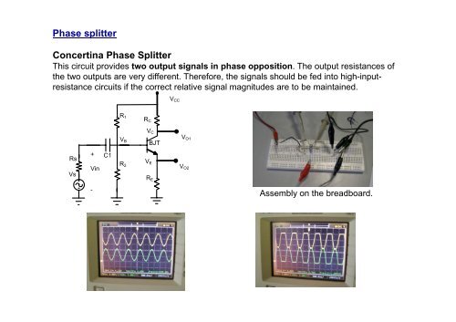
Phase splitter Concertina Phase Splitter
Phase splitter Concertina Phase Splitter
Phase splitter Concertina Phase Splitter

Create successful ePaper yourself
Turn your PDF publications into a flip-book with our unique Google optimized e-Paper software.
<strong>Phase</strong> <strong>splitter</strong><br />
<strong>Concertina</strong> <strong>Phase</strong> <strong>Splitter</strong><br />
This circuit provides two output signals in phase opposition. The output resistances of<br />
the two outputs are very different. Therefore, the signals should be fed into high-inputresistance<br />
circuits if the correct relative signal magnitudes are to be maintained.<br />
Rs<br />
Vs<br />
+<br />
Vin<br />
-<br />
C1<br />
R1<br />
VB<br />
R2<br />
RC<br />
VC<br />
BJT<br />
VE<br />
RE<br />
VCC<br />
VO1<br />
VO2<br />
Assembly on the breadboard.
<strong>Phase</strong> <strong>splitter</strong><br />
Synthesis<br />
The biasing voltages of the collector (V CQ) and emitter (V EQ) are chosen so to ensure<br />
maximum dynamic of the signals on the collector and emitter.<br />
V CQ=3V CC/4 e V EQ=V CC/4 consequently V CEQ=V CC/2<br />
1) On R C and R E there is the same voltage drop, therefore the two resistors must have the<br />
same value (R) which is obtained by the equation on the output mesh:<br />
R1<br />
R2<br />
V B<br />
I C<br />
BJT<br />
V CC<br />
Rc<br />
V CQ<br />
V EQ<br />
R E<br />
V −V<br />
VCC = I CQ·2·R+ VCEQ ⇒ R=<br />
I ·2<br />
2) Calculate R 2 :<br />
3) Calculate R 1:<br />
CC CEQ<br />
CQ<br />
1 1<br />
R2 = ⋅hFE ⋅ R = ⋅<br />
10 10<br />
h FE min·hFEmax ⋅R<br />
or<br />
VB R2= I<br />
VB =<br />
10⋅I VB<br />
=<br />
10⋅I<br />
⋅ h FE min·hFEmax R2BQ CQ<br />
V −V<br />
R = R<br />
CC B<br />
1<br />
VB<br />
2
<strong>Phase</strong> <strong>splitter</strong><br />
Long-tailed pair <strong>Phase</strong> <strong>Splitter</strong><br />
This circuit is known as a long-tailed pair because the two BJT's share the resistor REE. A signal applied at the CEC input causes an opposite signal Vout1 and a signal with same<br />
phase at the CBC input.<br />
So, the signal Vout2 has same phase of the signals at the input of the CBC.<br />
Consequently the signals Vout1and Vout2 have opposite phase.<br />
|Vout1|=|Vout2| results if the signal current iREE=0 (and iQ1=iQ2) or for real conditions |Vout1|º|Vout2| if iREE 100<br />
1+ h<br />
fe<br />
CEC<br />
For the BC107 (h ie=4kΩ, h fe=250)<br />
R EE > 1.6kΩ<br />
V in<br />
R1<br />
C1<br />
R2<br />
Rc<br />
V out1<br />
V CC<br />
Rc<br />
Q1 Q2<br />
i Q1<br />
i REE<br />
-V EE<br />
V out2<br />
R EE<br />
i Q2<br />
R1<br />
R2<br />
C2<br />
+<br />
CBC
C 1<br />
V in<br />
R 1<br />
V B1<br />
R 2<br />
V C1<br />
R c<br />
V out1<br />
V CC<br />
R c<br />
V out2<br />
Q1 Q2<br />
I REE<br />
V E<br />
R EE<br />
-V EE<br />
V C2<br />
R 1<br />
V B2<br />
R 2<br />
+<br />
C 2<br />
+<br />
V in<br />
Vout1 RCRC =− ≅− h<br />
V h + R h<br />
in ie ie<br />
-<br />
i b<br />
R 1//R 2<br />
fe<br />
h fei b<br />
h ie<br />
R C<br />
V out1<br />
R C<br />
R EE<br />
h fei b<br />
i b<br />
h ie<br />
hie hie<br />
R= R EE // ≅<br />
1+ h 1+ h<br />
fe fe
<strong>Phase</strong> <strong>splitter</strong><br />
Synthesis<br />
The circuit is symmetric so the emitter resistor can be divided in two parallel resistors with<br />
value 2REE and the synthesis can be done considering half circuit.<br />
The following assumptions are used VCC=-VEE=10V,VBEQ=0.65V, ICQ=1 mA,VCEQ=5V, VEQ=0. CC CEQ<br />
1) Calculate RC : RC= = 5kΩ<br />
ICQ<br />
2) Calculate 2R EE :<br />
3) Calculate R 2 :<br />
4) Calculate R 1:<br />
V −V<br />
VEQ + VEE10V 2REE = = = 10kΩ<br />
I 1mA<br />
CQ<br />
The R EE condition must be veryfied :<br />
For the BC107 h = h ⋅0.95 ≅ 211<br />
FE 1mA FE 2mA<br />
ICQ 1mA<br />
IR2 = 10I BQ = 10 ≅10 ≅47μ<br />
A<br />
h 211<br />
VB V BE 065 . V<br />
R2 = = ≅ ≅14kΩ<br />
I I 47μ<br />
A<br />
R2 R2<br />
FE 1mA<br />
VCC −VBE9.35V<br />
IR1 ≅ IR2→ R1= = ≅ 200kΩ<br />
I 47μA R1<br />
( )<br />
R > 100 ⋅ h / 1+ h<br />
EE ie fe<br />
R1<br />
R2<br />
V B<br />
I R1<br />
I R2<br />
I BQ<br />
I CQ<br />
BJT<br />
V CC<br />
Rc<br />
V CQ<br />
V EQ<br />
2R EE<br />
-V EE
Differential Amplifier<br />
This circuit allows to obtain an output signal<br />
proportional to the difference of the input signals.<br />
Where A d is the differential gain.<br />
v out = A d (v in1-v in2)<br />
On the other hand, there is an output signal also in<br />
thecaseofV IN1 =V IN2, this signal depends from (not<br />
desired) common mode amplification A C.Therefore<br />
for a real differential amplifier, in general, we can write:<br />
v out = A d (v in1-v in2) + A c (v in1+v in2)/2<br />
vin1<br />
RC<br />
BJT1<br />
REE<br />
VCC<br />
IC+ic1 IC+ic2<br />
ic1d=-ic2d<br />
-VEE<br />
BJT2<br />
RC<br />
2IC+2ic1c<br />
-V EE and R EE (R EE with high value) work as a current generator that:<br />
determines the bias current I C of the two BJT and<br />
contrasts the current variations of R EE.<br />
The collector currents (i c1, i c2) related to v in1, v in2 consist of two components:<br />
i = i + i ; i = i + i<br />
C3<br />
vin2<br />
c1 c1d c1c c2 c2d c2c One relative to the difference of the signals the other relative to the common mode signal.<br />
i = i ; i = - i<br />
The current generator requires that |i c1d|>>|i c1c| and |i c2d|>>|i c2c|.<br />
c2c c1c c1d c2d vout
v out = A d (v in1-v in2) + A c (v in1+v in2)/2<br />
RC<br />
BJT1<br />
VCC<br />
IC+icd1 IC+icd2<br />
ic1d= -ic2d<br />
REE<br />
2IC<br />
-VEE<br />
+ vd -<br />
BJT2<br />
C3<br />
vout<br />
v in1 = v d/2 and v in2 = -v d/2<br />
RC<br />
+<br />
Vc<br />
-<br />
vin1<br />
RC<br />
BJT1<br />
REE<br />
VCC<br />
IC+icc1 IC+icc2<br />
-VEE<br />
BJT2<br />
2IC+2icc1<br />
v in1 = v in2 = v c<br />
RC<br />
vin2<br />
C3<br />
vout<br />
+<br />
Vc<br />
-
The two amplifications can be estimated by considering two situations:<br />
1) V in1 = V in2 = V s<br />
+<br />
vS<br />
-<br />
vin1<br />
RC<br />
BJT1<br />
VCC<br />
IC+ics1 IC+ics2<br />
REE<br />
BJT2<br />
2IC+2ics1<br />
-VEE<br />
RC<br />
vin2<br />
C3<br />
vout<br />
+<br />
vS<br />
-<br />
A<br />
c<br />
vin1=vs<br />
RC<br />
2REE<br />
BJT1<br />
IC+ic1s IC+ic2s<br />
BJT2<br />
RC<br />
V Rh<br />
o<br />
C fe<br />
= =−<br />
V 2 h + 1+ h 2R<br />
( )<br />
2REE<br />
vout<br />
vin2=vs<br />
in ie fe EE<br />
ic2s<br />
BJT2<br />
RC<br />
2REE<br />
vout<br />
vin2=vs
2) V in1 = V d/2 and V in2 = -V d/2<br />
+<br />
vd/2<br />
-<br />
vin1<br />
RC<br />
BJT1<br />
VCC<br />
IC+icd1 IC+icd2<br />
REE<br />
ic1d<br />
2IC<br />
-VEE<br />
BJT2<br />
RC<br />
vin2<br />
C3<br />
vout<br />
-<br />
vd/2<br />
+<br />
vin1=vd/2<br />
BJT1<br />
Vo V Rh o V Rh<br />
o<br />
= =− ; Ad<br />
= =<br />
V 2 −V<br />
/ 2 h V 2h<br />
C fe C fe<br />
in d ie d ie<br />
Electronics: a systems approach by N. Storey<br />
RC<br />
IC+ic1d IC+ic2d<br />
E<br />
REE<br />
c<br />
BJT2<br />
RC<br />
C3<br />
vout<br />
v in2= - v d/2<br />
ic2d<br />
BJT2<br />
RC<br />
vout<br />
vin2=- vd/2<br />
The parameter, which specifies how the real amplifier is close to that ideal, is the<br />
common mode rejection ratio:<br />
Ad<br />
CMRR =<br />
A<br />
The behavior of the differential amplifier is close to that ideal if CMRR is great, in<br />
other words if A d is much larger than A c.
The differential stage which will be realized in experiments is shown in the figure.<br />
V in1<br />
R 1<br />
R C<br />
R 2<br />
BJT1<br />
i C1<br />
R EE<br />
For the biasing network, the synthesis procedure is the same of the long-tailed<br />
pair phase <strong>splitter</strong>.<br />
So dividing the circuit, knowing the V EE and V CC values and selecting the<br />
biasing voltages and currents of the components the biasing network can be<br />
defined.<br />
V CC<br />
i C2<br />
-V EE<br />
R C<br />
BJT2<br />
R 2<br />
R 1<br />
C 3<br />
V out<br />
V in2<br />
100kΩ C1 C<br />
A<br />
2 100kΩ<br />
R L
To measure the two amplification you can proceed in several ways, but two<br />
measures must be made, here are some methods.<br />
A) 1 st measure V in1=-V in2=V test, in this case A d =V out1/(2V test)<br />
2 nd measure V in1=V in2=V test, in this case A c =V out2/V test<br />
B) 1 st measure V in1= V test ,V in2=0, in this case V out1=A dV test+A cV test/2<br />
2 nd measure V in1= 0,V in2= V test, in this case V out2= -A dV test+A cV test/2<br />
V out2 is in phase opposition respect to V out1 so -V out2 is assumed, adding the two<br />
obtained output signals :<br />
V out1 +V out2 =A cV est A c= (V out1 +(-V out2))/V test<br />
V out1 -V out2 =2A dV test A d =(V out1 - (-V out2))/2V test<br />
C) 1 st measure V in1=V in2=V test, in this case A c =V out1/V test<br />
2 nd measure V in1= V test ,V in2=0, in this case V out2=A dV test+A cV test/2<br />
From which is obtained:<br />
A d =V out1 /V test -A c /2
v out = A d (v in1-v in2)<br />
v in1 non-inverting input<br />
v in2 inverting input<br />
vin 1<br />
R C<br />
BJT 1<br />
in1<br />
Volt.<br />
in2<br />
Volt.<br />
IC+i c1<br />
ic1d=-ic2d<br />
R EE<br />
V CC<br />
BJT1<br />
Cur.<br />
BJT2<br />
Cur.<br />
I C+i c2<br />
BJT2<br />
2I C+2i c1s<br />
-VEE<br />
R C<br />
BJT2<br />
Cur.<br />
Out<br />
Volt.<br />
C 3<br />
v in 2<br />
v ou t<br />
Out<br />
Volt.