Cantilever-like micromechanical sensors - Artek
Cantilever-like micromechanical sensors - Artek
Cantilever-like micromechanical sensors - Artek

Create successful ePaper yourself
Turn your PDF publications into a flip-book with our unique Google optimized e-Paper software.
Rep. Prog. Phys. 74 (2011) 036101 A Boisen et al<br />
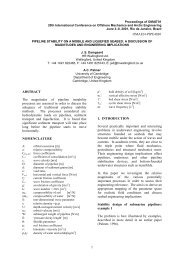
(a)<br />
(b)<br />
(c)<br />
(d)<br />
Si substrate<br />
photoresist<br />
Figure 9. Fabrication of silicon-based cantilevers by bulk<br />
micromachining: (a) substrate preparation by thin film deposition;<br />
(b) patterning of cantilevers by photolithography and etching;<br />
(c) cantilever release by etching through the bulk wafer from the<br />
backside and (d) removal of the etch stop layer.<br />
approach, where the suspended structures are defined by<br />
etching from the backside all the way through the wafer, is<br />
called bulk micromachining [94].<br />
The fabrication is based on single crystal silicon wafers<br />
with thicknesses of 350–500 µm. During substrate preparation<br />
thin films of the actual cantilever material such as silicon<br />
nitride, silicon oxide or poly-silicon are deposited. The<br />
thickness of these films defines the final thickness of the<br />
cantilevers. Usually, a three-layered substrate is prepared, see<br />
figure 9(a), where the intermediate material is the so-called<br />
etch stop layer. This material protects the actual device layer<br />
during the release in order to secure a well-defined thickness<br />
and a highly reflecting surface of the cantilever. A common<br />
method is the use of single crystal silicon wafers (1 0 0) with a<br />
built-in silicon oxide film. These wafers are also called siliconon-insulator<br />
(SOI) and can be ordered from a range of suppliers<br />
[95–97]. The cantilevers are defined by UV patterning of<br />
photoresist [98] on the front side of the wafer. For nanoscale<br />
cantilevers, the UV lithography can be replaced by electronbeam<br />
lithography [99]. The resist pattern is transferred to<br />
the device layer by wet etching [98] or reactive ion etching<br />
(RIE) [98], figure 9(b). The etching from the backside is<br />
achieved with potassium hydroxide (KOH) [98] or by deep<br />
reactive ion etching (DRIE) [100], figure 9(c). As a final<br />
step the etch stop layer is removed to release the cantilevers,<br />
figure 9(d).<br />
The process results in free-standing cantilevers, accessible<br />
from both sides of the wafer. This is often advantageous.<br />
Both sides of the cantilever can be easily inspected and the<br />
cantilever can be placed in a liquid or gas flow perpendicular<br />
to the cantilever where the etched holes in the wafer serve<br />
as microfluidic channels. However, the cantilevers are rather<br />
fragile and not well protected. Moreover, etching through the<br />
entire silicon wafer is time consuming.<br />
11<br />
In recent years, materials such as silicon carbide [101],<br />
graphene [102] and diamond-<strong>like</strong> carbon [103] have emerged<br />
as alternatives to silicon, all offering unique chemical and<br />
mechanical properties.<br />
3.2. Polymer-based devices<br />
3.2.1. Materials. Since the late 1990s, an increasing amount<br />
of work has been reported on the fabrication of polymer-based<br />
cantilevers. The main motivation to introduce polymers is that<br />
Young’s modulus typically is two orders of magnitude lower<br />
than for traditional silicon-based materials. Consequently,<br />
the stiffness of the cantilevers is reduced and the sensitivity<br />
increases. Equation (2.19) shows that the cantilever bending<br />
due to surface stress changes is directly proportional to Young’s<br />
modulus of the cantilever material. The increased sensitivity<br />
is achieved if the thickness of the polymer cantilevers is<br />
comparable to the ones fabricated using silicon. Another<br />
important driving force to evaluate various polymers and<br />
fabrication methods is the possibility to reduce costs of raw<br />
material and fabrication.<br />
In 1994, Pechmann and co-workers fabricated the<br />
first polymer microcantilevers with a standard Novolakbased<br />
photoresist as cantilever material [104]. In 1999,<br />
Genolet used the negative epoxy photo-resist SU-8 to define<br />
AFM-cantilevers [105]. Young’s modulus of SU-8 is low<br />
(around 4 GPa [106]) compared with silicon and silicon nitride<br />
(180 and 290 GPa, respectively) which makes it a suitable<br />
candidate for <strong>micromechanical</strong> structures for surface stress<br />
measurements [107, 108]. In parallel, a large number of wellknown<br />
polymers such as polyimide [109, 110], polystyrene<br />
[111–113], polypropylene [113], polyethylene therephtalate<br />
(PET) [114] and fluoropolymer [115] have been evaluated<br />
for the fabrication of <strong>micromechanical</strong> <strong>sensors</strong>. Recently,<br />
new thermoplasts specifically developed for microfabrication<br />
such as parylene [116, 117] and TOPAS® [118, 119] were<br />
introduced as cantilever materials.<br />
3.2.2. Surface micromachining. A typical process scheme<br />
for the fabrication of polymer cantilevers is illustrated in<br />
figure 10. Compared with silicon-based devices, the freestanding<br />
structures are fabricated by building up layers on<br />
the surface of a carrier substrate. This approach is called<br />
surface micromachining [120]. First, a so-called sacrificial<br />
layer is applied, figure 10(a), followed by deposition of a<br />
thin cantilever material. In most cases this is achieved by<br />
spin-coating an organic solution of a polymer. An interesting<br />
alternative is parylene, which is deposited by chemical vapour<br />
deposition using di-para(xylylene) [121].<br />
The most straightforward method to pattern the polymer<br />
cantilever is to use UV-photolithography, figure 10(b). This<br />
requires that the polymer is a photoresist such as SU-8 or<br />
polyimide [105, 107–109]. The thin polymer film defining<br />
the cantilevers is spin-coated, baked and exposed using<br />
standard equipment, which minimizes fabrication time and<br />
costs. An alternative approach is patterning the cantilevers<br />
by a combination of traditional photolithography and polymer<br />
etching. For example, O2-plasma etching has been used