High-Performance BiHEMT HBT / E-D pHEMT Integration - TriQuint ...
High-Performance BiHEMT HBT / E-D pHEMT Integration - TriQuint ...
High-Performance BiHEMT HBT / E-D pHEMT Integration - TriQuint ...

Create successful ePaper yourself
Turn your PDF publications into a flip-book with our unique Google optimized e-Paper software.
<strong>High</strong>-<strong>Performance</strong> <strong>BiHEMT</strong> <strong>HBT</strong> / E-D <strong>pHEMT</strong> <strong>Integration</strong><br />
T. Henderson, J. Middleton, J. Mahoney, S. Varma, T. Rivers, C. Jordan, and B. Avrit<br />
<strong>TriQuint</strong> Semiconductor<br />
2300 NE Brookwood Parkway<br />
Hillsboro, OR 97124<br />
(503)615-9301<br />
thenderson@tqs.com<br />
Abstract<br />
We report on the status of <strong>TriQuint</strong>’s <strong>BiHEMT</strong> process --<br />
the cointegration of <strong>TriQuint</strong>’s InGaP/GaAs <strong>HBT</strong> power<br />
amplifier technology with an InGaAs/AlGaAs E/D-Mode<br />
<strong>pHEMT</strong> technology into a single GaAs process. This added<br />
<strong>pHEMT</strong> functionality over previously reported GaAs<br />
<strong>HBT</strong>/FET cointegration technologies adds an additional level<br />
of versatility and potential circuit applications. Potential<br />
applications include the cointegration of <strong>HBT</strong> power<br />
amplifier circuitry with <strong>pHEMT</strong>-based bias control and logic<br />
circuitry, RF switches, and low noise amplifiers. The growth<br />
and process technologies developed for this process, as well as<br />
the preliminary device characteristics and process features,<br />
will be described. Finally, we will describe the process and<br />
performance tradeoffs featured in the <strong>BiHEMT</strong> process.<br />
INTRODUCTION<br />
The idea of cointegration of <strong>HBT</strong>s and FETs on GaAs<br />
has long been of wide interest [1-3] in the GaAs<br />
community. Of course, the principle attraction is in<br />
improving circuit functionality, analogous to Si BiCMOS<br />
technology. Recently, there has been a great deal of<br />
interest in combined <strong>HBT</strong>/FET processes for enhanced<br />
circuit functionality, particularly for power amplifier<br />
circuits. With a combined <strong>HBT</strong>/FET technology in GaAs,<br />
<strong>HBT</strong>s may be used for linear power amplification and<br />
FETs for logic and control circuitry, RF switches, and low<br />
noise power amplification. Two distinct approaches, each<br />
with their own advantages, have been described recently.<br />
One features manufacturability and simplicity of process at<br />
the expense of device performance by cointegrating a<br />
MESFET structure into the emitter of the <strong>HBT</strong> [4]. The<br />
other offers improved device performance by cointegrating<br />
a <strong>pHEMT</strong> epitaxial structure in the subcollector of the<br />
<strong>HBT</strong> [5], at the expense of additional processing steps and<br />
more complex crystal growth. However, in the latter<br />
approach the <strong>pHEMT</strong> epitaxy and process still represent a<br />
compromise between compatibility with the <strong>HBT</strong> epitaxial<br />
structure and device performance.<br />
In the <strong>BiHEMT</strong> approach reported here, the design goals<br />
are somewhat different from those reported previously<br />
[4,5], with a goal of maximizing <strong>pHEMT</strong> functionality and<br />
device performance (while maintaining minimal impact on<br />
<strong>HBT</strong> performance) for improved circuit functionality. The<br />
result is a novel epitaxial design and process architecture<br />
that replicate as closely as possible <strong>TriQuint</strong>’s existing<br />
<strong>HBT</strong> and E/D <strong>pHEMT</strong> processes.<br />
EPITAXIAL LAYER DESIGN AND GROWTH<br />
The epitaxial structure is relatively straightforward.<br />
Aside from several minor modifications that are driven by<br />
process considerations, the <strong>BiHEMT</strong> epitaxial structure<br />
consists of the <strong>TriQuint</strong> <strong>HBT</strong> epitaxial structure on top of<br />
the <strong>TriQuint</strong> E/D <strong>pHEMT</strong> epitaxial structure.<br />
In order to minimize <strong>BiHEMT</strong> cost, a single MOCVD<br />
growth is used for the entire epitaxial structure, without the<br />
need for regrowth or intermediate processing. The<br />
requirement of high <strong>pHEMT</strong> performance necessitates<br />
placement of the entire InGaAs/AlGaAs <strong>pHEMT</strong> epitaxial<br />
stack underneath the <strong>HBT</strong> subcollector. In other words,<br />
there is no part of the <strong>HBT</strong> subcollector proper that is used<br />
in the active <strong>pHEMT</strong> device, unlike the case reported in<br />
[5]. That way, not only is the <strong>pHEMT</strong> well isolated from<br />
parasitic capacitances, but no compromises in epitaxial<br />
structure are made that might lead to significantly<br />
degraded performance. Naturally, special care needs to be<br />
taken to ensure minimal degradation in <strong>pHEMT</strong><br />
characteristics during the long subsequent <strong>HBT</strong> growth. A<br />
key requirement of a high-performance <strong>pHEMT</strong> device is<br />
high maximum current Imax and minimal on-resistance Ron;<br />
some small modifications in the <strong>pHEMT</strong> epitaxial<br />
structure must be made in order to minimize <strong>pHEMT</strong><br />
epitaxy degradation during the subsequent <strong>HBT</strong> growth.<br />
Maintaining the Imax and Ron of the original E/D <strong>pHEMT</strong><br />
process in the <strong>BiHEMT</strong> process is challenging.<br />
Of course the <strong>pHEMT</strong> epitaxy technically forms a part<br />
of the subcollector of the <strong>HBT</strong>, since it is a conductive<br />
region immediately underneath the subcollector.<br />
Nonetheless, the sheet conductivity of the <strong>pHEMT</strong><br />
structure is negligible in comparison to that of the<br />
subcollector, as the <strong>pHEMT</strong> active layers are relatively<br />
thin compared to the subcollector. Since precision is<br />
required in etching to the appropriate <strong>pHEMT</strong> epilayer,<br />
etch stop layers are required for process ease at several<br />
points in the epitaxy. These layers are intentionally kept<br />
thin to avoid process complexity. Their effect on <strong>HBT</strong><br />
thermal resistance is minimal, since they are underneath<br />
the active <strong>HBT</strong> epitaxial layers and where the <strong>HBT</strong>
structure is physically widest. Additionally, a large part of<br />
<strong>HBT</strong> self-heating is dissipated through a thermal shunt on<br />
top of the active emitter.<br />
DEVICE FABRICATION<br />
The <strong>BiHEMT</strong> process represents a modification of<br />
<strong>TriQuint</strong>’s <strong>HBT</strong> process, with <strong>pHEMT</strong> specific steps<br />
inserted between the <strong>HBT</strong> device-specific process steps<br />
and the passive/interconnects metallization formation.<br />
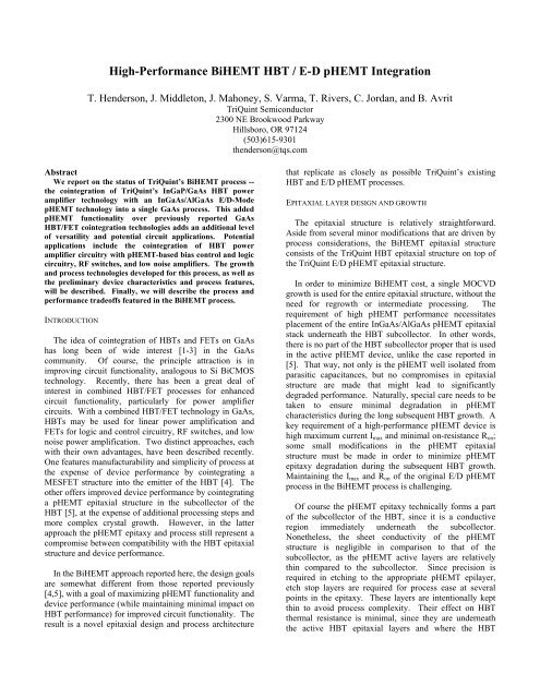
Fig. 1 shows a cross-sectional schematic of <strong>TriQuint</strong>’s<br />
<strong>HBT</strong> and E/D <strong>pHEMT</strong> technology. Device fabrication is<br />
relatively straightforward, with four types of process steps:<br />
<strong>HBT</strong>-specific metallization, such as at emitter and base;<br />
etches that uncover the different <strong>HBT</strong> and <strong>pHEMT</strong> epi<br />
layers; <strong>pHEMT</strong>-gate processing; and the fabrication of<br />
common structures, such as capacitors, resistors, and metal<br />
interconnects. In order to reduce process complexity,<br />
several device-specific process steps, such as <strong>HBT</strong><br />
collector and <strong>pHEMT</strong> source/drain ohmic metallization are<br />
combined. No degradation is seen in either <strong>pHEMT</strong> or<br />
<strong>HBT</strong> device characteristics as a result of this consolidation.<br />
Fabrication starts with standard <strong>HBT</strong> processing modules,<br />
including emitter metallization, emitter mesa formation,<br />
and base metallization.<br />
Then, the base mesa is formed by etching all the way<br />
down to an etch stop at the top of the subcollector. Once<br />
the subcollector is reached, an additional etch step is added<br />
that etches away the subcollector in the field, in order to<br />
uncover the <strong>pHEMT</strong> epitaxial structure. <strong>pHEMT</strong><br />
processing then begins with wide recess pattern<br />
lithography and etch, and a shallow implant is performed<br />
into the remaining <strong>pHEMT</strong> epi in the field in order to<br />
electrically isolate all devices.<br />
After the implant, a common <strong>HBT</strong>/<strong>pHEMT</strong> ohmic<br />
metallization is done, with the collector metallization<br />
sitting on top of the subcollector for the <strong>HBT</strong> and lower<br />
down in the epi, on top of the cap layer, for the <strong>pHEMT</strong>s.<br />
Following ohmic contact formation comes the proprietary<br />
D-mode and E-mode narrow recess formations and gate<br />
depositions; for both types of device, etch stops facilitate<br />
the recess and 0.7 um gates are formed. Here we note that<br />
our usual E/D process employs a 0.5 um gate. A 0.5 um<br />
gate <strong>BiHEMT</strong> process is currently under development, but<br />
narrow gate lithography is considerably complicated by the<br />
highly nonplanar <strong>BiHEMT</strong> structure.<br />
After <strong>HBT</strong> and <strong>pHEMT</strong> device formation, 50<br />
ohm/square NiCr resistors are formed, as well as MIM<br />
capacitors with 1200 pF/mm 2 capacitance. The bottom of<br />
the MIM layer is used as a local interconnect, and<br />
subsequent plated gold layers of 2 um and 4 um thickness<br />
are used for global interconnects. Finally, the entire<br />
Dielectric<br />
D-Mode<br />
<strong>pHEMT</strong><br />
Figure 1. Cross section of <strong>TriQuint</strong>’s <strong>BiHEMT</strong> process,<br />
showing GaAs/InGaP <strong>HBT</strong>, D-mode AlGaAs/InGaAs<br />
<strong>pHEMT</strong>, E-mode AlGaAs/InGaAs <strong>pHEMT</strong>, resistors,<br />
capacitors, and three levels of interconnect metal.<br />
structure is covered by a thick layer of nitride for<br />
passivation, and wafer thinning and through via formation<br />
follow.<br />
<strong>BiHEMT</strong> DEVICE CHARACTERIZATION<br />
As previously mentioned, <strong>HBT</strong>-specific epitaxy and<br />
process in the <strong>BiHEMT</strong> process are for the most part<br />
unchanged from the standard <strong>HBT</strong> process. As a result,<br />
most <strong>HBT</strong> device parameters – both DC and RF – are<br />
substantially the same as they are in the original <strong>TriQuint</strong><br />
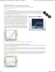
<strong>HBT</strong> power amplifier process. Fig. 2(a) and (b) shows<br />
representative Gummel plot and common-emitter I-V<br />
characteristics for a 3x(3x45) um 2 emitter <strong>HBT</strong>. Typical<br />
beta is 80 and BVcbo = 24 V, with Ft = 30 GHz and Fmax =<br />
55 GHz.<br />
There are only two significant differences in <strong>HBT</strong><br />
characteristics between the <strong>BiHEMT</strong> <strong>HBT</strong> and our<br />
dedicated <strong>HBT</strong> process. First, the <strong>BiHEMT</strong> <strong>HBT</strong> has a<br />
slightly higher collector resistance. This is because in the<br />
Ic (A)<br />
0.10<br />
0.08<br />
0.06<br />
0.04<br />
0.02<br />
0.00<br />
E-Mode<br />
<strong>pHEMT</strong><br />
Metal2 – 4 um<br />
Metal1 – 2 um<br />
Dielectric<br />
InGaP/GaAs<br />
<strong>HBT</strong><br />
Semi-Insulating GaAs Substrate<br />
0.0 1.0 2.0 3.0 4.0<br />
V ce (V)<br />
Fig. 2(a). Common-emitter I-V for a 3x(3x45) um 2 emitter<br />
<strong>HBT</strong> in the <strong>BiHEMT</strong> process.<br />
NiCr<br />
MIM<br />
Isolation Implant<br />
Metal0
Ic, Ib (A)<br />
1.E+00<br />
1.E-03<br />
1.E-06<br />
1.E-09<br />
1.E-12<br />
0.0 0.5 1.0 1.5<br />
V be (V)<br />
Fig. 2(b). Gummel plot for the <strong>HBT</strong> in Fig. 2(a).<br />
<strong>BiHEMT</strong> process, the subcollector is grown thinner in<br />
order to reduce nonplanarity, as this layer has to be etched<br />
completely off in the field. Second -- and related to this --<br />
isolation and leakage current between <strong>HBT</strong> structures is<br />
lower in the <strong>BiHEMT</strong> process, because the remaining<br />
epitaxy in the field is thinner and can be isolated with a<br />
shallower, lower dose isolation implant than is the case<br />
with the <strong>HBT</strong> process.<br />
As expected, <strong>BiHEMT</strong> FET performance is similar to<br />
that of our nominal E/D <strong>pHEMT</strong> process performance, but<br />
with some change seen due to the 0.7 um gates in the<br />
<strong>BiHEMT</strong>. Fig. 3(a) shows the DC I-V characteristics of a<br />
typical D-mode device with a 0.7 um gate and 150 um gate<br />
width. Fig. 3(b) shows the transfer characteristics. As<br />
shown, peak gm is 300 mS/mm, Idss is 160 mA/mm, and<br />
Imax is 420 mA/mm. Pinchoff voltage Vp is -0.8 V, gatedrain<br />
breakdown voltage BVgdo is 22 V, and on resistance<br />
Ron is 2.0 ohm-mm. RF characteristics include a typical Ft<br />
of 20 GHz and an Fmax of 57 GHz.<br />
Ids (mA/mm)<br />
400<br />
300<br />
200<br />
100<br />
0<br />
0 2 4 6<br />
Vds (V)<br />
Fig. 3(a). DC I-V characteristics of a D-Mode <strong>pHEMT</strong><br />
with 0.7 um gate length and 150 um gate width. Vg = -0.8<br />
to 0.8 V, in 0.2 V steps.<br />
Id (mA/mm), gm (mS/mm)<br />
500<br />
400<br />
300<br />
200<br />
100<br />
0<br />
-1.0 -0.5 0.0 0.5 1.0<br />
V gs (V)<br />
Fig. 3(b). Transfer curves for the D-mode <strong>pHEMT</strong> in Fig.<br />
3(a) for Vd = 2 V.<br />
DC I-V characteristics of a typical E-mode <strong>BiHEMT</strong><br />
device are shown in Fig. 4(a) for a device with a 0.7 um<br />
gate length and 150 um gate width. Fig. 4(b) shows the<br />
transfer characteristics. As shown, peak gm is 460 mS/mm<br />
and Imax is 240 mA/mm. Pinchoff voltage Vp is +0.3 V,<br />
Id (mA/mm)<br />
300<br />
200<br />
100<br />
0<br />
0 2 4 6<br />
Vds (V)<br />
Fig. 4(a). DC I-V characteristics of a E-Mode <strong>pHEMT</strong><br />
with 0.7 um gate length and 150 um gate width. Vg = 0.2<br />
to 0.8 V, in 0.1 V steps.<br />
Id (mA/mm), gm (mS/mm)<br />
500<br />
400<br />
300<br />
200<br />
100<br />
0<br />
-1.0 -0.5 0.0 0.5 1.0<br />
Vgs (V)<br />
Fig. 4(b). Transfer curves for the E-mode <strong>pHEMT</strong> in Fig.<br />
3(a) for Vd = 2 V.
gate-drain breakdown voltage BVgdo is 23 V, and on<br />
resistance Ron is 2.3 ohm-mm. RF characteristics include a<br />
typical Ft of 22 GHz and an Fmax of 65 GHz. Future work<br />
will focus on improving <strong>pHEMT</strong> performance (focusing<br />
on the development of a 0.5 um gate process) and ramping<br />
the <strong>BiHEMT</strong> process to volume production.<br />
SUMMARY<br />
We have described <strong>TriQuint</strong>’s <strong>BiHEMT</strong> process.<br />
Applications for this technology include the cointegration<br />
of <strong>HBT</strong> power amplifiers with E/D <strong>pHEMT</strong>-based logic<br />
and control circuitry, RF switches, and low noise power<br />
amplifiers. This process features three levels of metal, 50<br />
ohm/square resistors, and 1200 pF/mm 2 MIM capacitors.<br />
The epitaxial structure is a unique combination of our<br />
existing <strong>HBT</strong> and E/D <strong>pHEMT</strong> epitaxy, and fabrication is<br />
optimized to deliver the highest level of transistor<br />
performance possible. The <strong>HBT</strong>s exhibit nearly identical<br />
performance to our existing <strong>HBT</strong> power amplifier process;<br />
the E/D <strong>pHEMT</strong>s feature 0.7 um gates with good RF<br />
performance, high current density, and low on-resistances.<br />
ACKNOWLEDGEMENTS<br />
The authors gratefully acknowledge the encouragement<br />
and support of Dr. Otto Berger, as well as the support of<br />
the staff of the <strong>TriQuint</strong> Oregon Fab Operations group.<br />
Also acknowledged are the technical support of B.<br />
Berggren and useful discussions with T. Apel, W. Howell,<br />
P. Litzenberg, L. Liu, K. Mays, C. Nevers, A. Ping, M.<br />
Porter, F. Radulescu, A. St. Denis, M. Wilson, and P.<br />
Wright.<br />
REFERENCES<br />
1. D.L. Plumton, et al., “Method to Integrate <strong>HBT</strong>s and<br />
FETs”, U.S. Patent No. 5,077,231 (1989).<br />
2. D. Cheskis, et al., IEDM Tech. Digest, pp. 91-94<br />
(1992).<br />
3. D. Streit, et al., GaAs IC Symp. Tech. Digest, pp.<br />
329-332 (1994).<br />
4. M. Sun et al., Proc. CS MANTECH Conf., pp. 149-<br />
152 (2006).<br />
5. M. Shokrani et al., Proc. CS MANTECH Conf., pp.<br />
153-156 (2006).