A High-Efficiency, Small-Size GaN Doherty Amplifier for LTE Micro ...
A High-Efficiency, Small-Size GaN Doherty Amplifier for LTE Micro ...
A High-Efficiency, Small-Size GaN Doherty Amplifier for LTE Micro ...

Create successful ePaper yourself
Turn your PDF publications into a flip-book with our unique Google optimized e-Paper software.
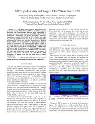
power is about 25W; gain is approximately 16dB; the<br />
maximum saturated efficiency is approximately 75%.<br />
Fig. 2 T1G6001528-Q3 package<br />
T1G6001528-Q3 package is show as Fig.2, the device<br />
dimension except input / output lead is 5mm x 6mm. The<br />
per<strong>for</strong>mance of this small device comes from its high power<br />
density. The small <strong>for</strong>m factor of the transistor is a key factor<br />
that enables development of a smaller-scale <strong>Doherty</strong> amplifier.<br />
The T1G6001528-Q3 provided this per<strong>for</strong>mance: Vd=28V,<br />
Idq=100mA, at pulse wave<strong>for</strong>m PW=50uS, duty=10%, its<br />
load-pull data at 2.65GHz is measured as following in Fig. 3.<br />
The reported <strong>Doherty</strong> amplifier is designed based on this loadpull<br />
data.<br />
Fig. 3 T1G6001528-Q3 load-pull data<br />
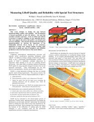
III. DOHERTY AMPLIFIER CONFIGURATION<br />
A symmetric <strong>Doherty</strong> amplifier is a very popular RF high<br />
power, high efficiency amplifier configuration <strong>for</strong><br />
contemporary wireless base stations. The amplifier<br />
demonstrated in this paper is designed using two<br />
T1G6001528-Q3 discrete packaged HEMTs, and the whole<br />
<strong>Doherty</strong> amplifier size is 30mm x 70mm as shown as Fig. 4.<br />
The small size is very necessary <strong>for</strong> micro-cell base stations or<br />
active antenna systems base stations where space is at a<br />
minimum.<br />
RF in<br />
Bias Vgs≈-‐3.7V<br />
Idq=100mA<br />
Bias Vgs=-‐5V<br />
Carrier amplifier<br />
T1G6001528-‐Q3<br />
Peakingamplifier<br />
T1G6001528-‐Q3<br />
28V Vds<br />
28V Vds<br />
Fig. 4 30mm x 70mm <strong>Doherty</strong> <strong>Amplifier</strong> Board<br />
RF out<br />
The amplifier PCB material is Taconic RF35B, with a<br />
thickness (H) of 16.6mm, and a dielectric constant (εr) of<br />
3.66.<br />
There is a 3dB hybrid at the input area, which is used to<br />
split the input signal into a carrier amplifier (the up path) and a<br />
peaking amplifier (the down path). The carrier amplifier is<br />
biased in class AB at Idq=100mA; the peaking amplifier is<br />
biased in class C mode. Since the carrier amplifier and<br />
peaking amplifier operate in different modes, their output<br />
impedances are not identical, so their output matching<br />
circuitry is slightly different.<br />
When designing a <strong>Doherty</strong> amplifier, the ideal situation is<br />
to design load impedance at Zopt equal to the maximum Psat<br />
point, and design load impedance at 2*Zopt equal to the<br />
maximum efficiency point. But because the T1G6001528-Q3<br />
is a wideband general purpose device, it is not specifically<br />
designed <strong>for</strong> 2.65 GHz <strong>Doherty</strong> purposes; its maximum<br />
efficiency is not at a 2:1 VSWR circle of the maximum<br />
saturated power. When we designed this <strong>Doherty</strong> amplifier,<br />
we had to compromise the load impedance at Zopt and 2 *<br />
Zopt. This means the load impedance at Zopt is not at the<br />
maximum saturated power point and the load impedance at 2 *<br />
Zopt is not at the maximum efficiency point.<br />
IV. DOHERTY AMPLIFIER PERFORMANCE<br />
The <strong>Doherty</strong> amplifier utilizing the T1G6001528-Q3 (as<br />
documented in Fig 3) has been measured with several kinds of<br />
signal wave<strong>for</strong>ms to characterize its per<strong>for</strong>mance <strong>for</strong> base<br />
station applications.<br />
Fig.5 shows its AM/AM and AM/PM curve, which is a<br />
critical parameter <strong>for</strong> DPD correction per<strong>for</strong>mance. In a<br />
typical normal LDMOS device <strong>Doherty</strong> amplifier, phase<br />
always drops when input power increases, which will reduce<br />
DPD correction per<strong>for</strong>mance. But in this amplifier utilizing<br />
the T1G6001528-Q3, phase variation of input power is totally<br />
different, which will be a benefit <strong>for</strong> DPD correction.