A High-Efficiency, Small-Size GaN Doherty Amplifier for LTE Micro ...
A High-Efficiency, Small-Size GaN Doherty Amplifier for LTE Micro ...
A High-Efficiency, Small-Size GaN Doherty Amplifier for LTE Micro ...

Create successful ePaper yourself
Turn your PDF publications into a flip-book with our unique Google optimized e-Paper software.
A <strong>High</strong>-<strong>Efficiency</strong>, <strong>Small</strong>-<strong>Size</strong> <strong>GaN</strong> <strong>Doherty</strong> <strong>Amplifier</strong><br />
<strong>for</strong> <strong>LTE</strong> <strong>Micro</strong>-Cell and Active Antenna System Applications<br />
Peter Xia, Milos Jankovic<br />
TriQuint Semiconductor, 500 W Renner Road, Richardson, TX , 75080, USA<br />
E-mail address: peter.xia@tqs.com<br />
Abstract — In this paper a high-efficiency, small-size <strong>GaN</strong><br />
<strong>Doherty</strong> amplifier <strong>for</strong> <strong>LTE</strong> micro-cell base station and active<br />
antenna systems base station application is presented. It is<br />
implemented with a TriQuint Semiconductor wideband discrete<br />
<strong>GaN</strong> RF power transistor, theT1G6001528-Q3. <strong>Doherty</strong><br />
amplifier per<strong>for</strong>mance is in the <strong>LTE</strong> standard frequency range<br />
2.62 GHz ~2.69 GHz; average output power=38.5dBm; the peak<br />
saturated output power is >46dBm; drain efficiency is >55%;<br />
gain is >15dB; 2 carrier 2x10 MHz; 8dB PAR <strong>LTE</strong> signal<br />
wave<strong>for</strong>m with Netlogic standard DPD; ACPR is better than -<br />
50dBc; <strong>Doherty</strong> amplifier size 30mm x 70mm.<br />
Index Terms — <strong>GaN</strong>, <strong>Doherty</strong> <strong>Amplifier</strong>, <strong>LTE</strong>, <strong>Micro</strong>-Cell,<br />
Active Antenna System, Base Station.<br />
I. INTRODUCTION<br />
In today’s communications networks, achieving higher data<br />
rates and spectrum efficiency are always motivations <strong>for</strong><br />
developing new technology. In order to meet the increasingly<br />
more stringent requirements of high data rate and high<br />
spectrum efficiency demanded by wireless<br />
telecommunications subscribers, the 4G wireless system<br />
including Long Term Evolution (<strong>LTE</strong>) have been developed to<br />
take advantage of some new technology. For example:<br />
Orthogonal Frequency Division Multiplexing ( OFDM ) and<br />
Multiple Input Multiple Output ( MIMO ) , which have<br />
properties of higher data rates and higher spectral efficiency in<br />
20 MHz signal bandwidth; downlink data rates of 100<br />
megabits per second ( Mbps ) and an uplink data rate of 50<br />
Mbps can be achieved. <strong>LTE</strong> modulation signal bandwidth is<br />
10 MHz <strong>for</strong> one carrier and 20MHz <strong>for</strong> two carriers. In order<br />
to provide a high data rate while consuming less power, small<br />
size base stations such as a micro-cell base stations or an<br />
active antenna system base station will be utilized more<br />
frequently in <strong>LTE</strong>-based networks than in W-CDMA (3G)<br />
networks. In this type of small-size wireless base station, highefficiency<br />
and small-sized RF power amplifiers are necessary<br />
to provide the per<strong>for</strong>mance required as cost-effectively as<br />
possible.<br />
Due to higher efficiency at a 6~10dB back-off range and<br />
better linearity with a digital pre-distortion ( DPD ) system,<br />
<strong>Doherty</strong> amplifier configurations are popularly used in<br />
wireless base station RF power amplifiers [1]~[2]. Although<br />
there are now some new advanced technology being<br />
developed <strong>for</strong> wireless base-station RF power amplifiers<br />
[3]~[4], high power and high efficiency RF amplifier<br />
configuration utilizing a <strong>Doherty</strong> amplifier configuration still<br />
is the most common wireless base station technology in mass<br />
production.<br />
A gallium nitride (<strong>GaN</strong>) RF power transistor, due to its high<br />
efficiency and high power density, has characteristics<br />
supporting the needs of next-generation RF power device<br />
applications [5]~[7] and was there<strong>for</strong>e the technology of<br />
choice <strong>for</strong> implementing this amplifier design.<br />
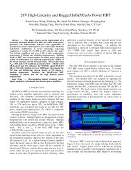
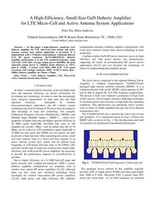
II. RF GAN POWER DEVICE<br />
The active device employed in the reported <strong>Doherty</strong> Power<br />
<strong>Amplifier</strong> is TriQuint Semiconductor T1G6001528-Q3<br />
packaged high electron mobility transistor (HEMT). It is a<br />
wideband discrete <strong>GaN</strong> on SiC HEMT, which operates at 28V<br />
and be able to support DC to 6 GHz frequency requirements.<br />
The device is built with TriQuint’s production 0.25μm <strong>GaN</strong><br />
on SiC process, which features advances field plate techniques<br />
to maximize power and efficiency at high drain bias operating<br />
conditions. This optimization can potentially lower systems<br />
costs in terms of simple amplifier line-ups and lower thermal<br />
management costs.<br />
The T1G6001528-Q3 uses a discrete die with 5 mm of total<br />
gate periphery. It is constructed based on four, 1.25mm unit<br />
HEMT cells, as shown in Fig. 1. The die placement and bond<br />
wire profiles are optimized <strong>for</strong> broadband per<strong>for</strong>mance.<br />
Fig. 1. T1G6001528-Q3 <strong>GaN</strong> transistor 1.25mm unit cell<br />
The packaged device utilized in this amplifier typically<br />
provides 18W of output power (P3dB) and linear gain higher<br />
than 10dB at 6 GHz. Maximum PAE is greater than 50%<br />
across the whole band. At 2.6 GHz frequency, its saturated
power is about 25W; gain is approximately 16dB; the<br />
maximum saturated efficiency is approximately 75%.<br />
Fig. 2 T1G6001528-Q3 package<br />
T1G6001528-Q3 package is show as Fig.2, the device<br />
dimension except input / output lead is 5mm x 6mm. The<br />
per<strong>for</strong>mance of this small device comes from its high power<br />
density. The small <strong>for</strong>m factor of the transistor is a key factor<br />
that enables development of a smaller-scale <strong>Doherty</strong> amplifier.<br />
The T1G6001528-Q3 provided this per<strong>for</strong>mance: Vd=28V,<br />
Idq=100mA, at pulse wave<strong>for</strong>m PW=50uS, duty=10%, its<br />
load-pull data at 2.65GHz is measured as following in Fig. 3.<br />
The reported <strong>Doherty</strong> amplifier is designed based on this loadpull<br />
data.<br />
Fig. 3 T1G6001528-Q3 load-pull data<br />
III. DOHERTY AMPLIFIER CONFIGURATION<br />
A symmetric <strong>Doherty</strong> amplifier is a very popular RF high<br />
power, high efficiency amplifier configuration <strong>for</strong><br />
contemporary wireless base stations. The amplifier<br />
demonstrated in this paper is designed using two<br />
T1G6001528-Q3 discrete packaged HEMTs, and the whole<br />
<strong>Doherty</strong> amplifier size is 30mm x 70mm as shown as Fig. 4.<br />
The small size is very necessary <strong>for</strong> micro-cell base stations or<br />
active antenna systems base stations where space is at a<br />
minimum.<br />
RF in<br />
Bias Vgs≈-‐3.7V<br />
Idq=100mA<br />
Bias Vgs=-‐5V<br />
Carrier amplifier<br />
T1G6001528-‐Q3<br />
Peakingamplifier<br />
T1G6001528-‐Q3<br />
28V Vds<br />
28V Vds<br />
Fig. 4 30mm x 70mm <strong>Doherty</strong> <strong>Amplifier</strong> Board<br />
RF out<br />
The amplifier PCB material is Taconic RF35B, with a<br />
thickness (H) of 16.6mm, and a dielectric constant (εr) of<br />
3.66.<br />
There is a 3dB hybrid at the input area, which is used to<br />
split the input signal into a carrier amplifier (the up path) and a<br />
peaking amplifier (the down path). The carrier amplifier is<br />
biased in class AB at Idq=100mA; the peaking amplifier is<br />
biased in class C mode. Since the carrier amplifier and<br />
peaking amplifier operate in different modes, their output<br />
impedances are not identical, so their output matching<br />
circuitry is slightly different.<br />
When designing a <strong>Doherty</strong> amplifier, the ideal situation is<br />
to design load impedance at Zopt equal to the maximum Psat<br />
point, and design load impedance at 2*Zopt equal to the<br />
maximum efficiency point. But because the T1G6001528-Q3<br />
is a wideband general purpose device, it is not specifically<br />
designed <strong>for</strong> 2.65 GHz <strong>Doherty</strong> purposes; its maximum<br />
efficiency is not at a 2:1 VSWR circle of the maximum<br />
saturated power. When we designed this <strong>Doherty</strong> amplifier,<br />
we had to compromise the load impedance at Zopt and 2 *<br />
Zopt. This means the load impedance at Zopt is not at the<br />
maximum saturated power point and the load impedance at 2 *<br />
Zopt is not at the maximum efficiency point.<br />
IV. DOHERTY AMPLIFIER PERFORMANCE<br />
The <strong>Doherty</strong> amplifier utilizing the T1G6001528-Q3 (as<br />
documented in Fig 3) has been measured with several kinds of<br />
signal wave<strong>for</strong>ms to characterize its per<strong>for</strong>mance <strong>for</strong> base<br />
station applications.<br />
Fig.5 shows its AM/AM and AM/PM curve, which is a<br />
critical parameter <strong>for</strong> DPD correction per<strong>for</strong>mance. In a<br />
typical normal LDMOS device <strong>Doherty</strong> amplifier, phase<br />
always drops when input power increases, which will reduce<br />
DPD correction per<strong>for</strong>mance. But in this amplifier utilizing<br />
the T1G6001528-Q3, phase variation of input power is totally<br />
different, which will be a benefit <strong>for</strong> DPD correction.
Fig.6 shows its PAR and efficiency variation with output<br />
power, which is measured at 2.65GHz, the WCDMA signal<br />
wave<strong>for</strong>m with PAR @ 0. 01% CCDF = 10.2dB.<br />
Fig. 7 shows its high power per<strong>for</strong>mance over the standard<br />
<strong>LTE</strong> frequency range of approximately 2.62GHz to 2.69GHz,<br />
which is measured with a WCDMA signal wave<strong>for</strong>m, the<br />
data is tested at 38dBm average output power, the saturated<br />
power is calculated using an average output power plus PAR.<br />
It can be seen from Fig.7 that in a standard <strong>LTE</strong> frequency<br />
range (2620 MHz~2690 MHz), when average output power at<br />
38dBm, its efficiency is higher than 55%.<br />
In contemporary base station designs, the RF power<br />
amplifier output need varies when the number of phones<br />
calling users within a given geographic area varies. This<br />
requirement is called “traffic control”. In order to let base<br />
stations always operate at high efficiency, generally the<br />
variation of output power is implemented through adjusting<br />
RF power amplifier working voltages. So that the base station<br />
Gain(dB)<br />
17<br />
16<br />
15<br />
14<br />
13<br />
12<br />
11<br />
10<br />
Output_PAR(dB)<br />
15<br />
13<br />
11<br />
9<br />
7<br />
5<br />
2.65GHz AM/AM & AM/PM<br />
Gain<br />
Phase<br />
13 15 17 19 21 23 25 27 29 31 33<br />
Pin( dBm)<br />
Fig. 5 AM/AM and AM/PM<br />
T1G6001528 <strong>Doherty</strong> Output PAR and <strong>Efficiency</strong> vs. Pout<br />
1C-‐WCDMA , 10.2dB PAR at 0.01%CCDF<br />
30 31 32 33 34 35 36 37 38 39<br />
Pout (dBm )<br />
130<br />
128<br />
126<br />
124<br />
122<br />
120<br />
118<br />
116<br />
Phase(° )<br />
AM/AM<br />
AM/PM<br />
Fig. 6 PAR and efficiency variation with output power<br />
60<br />
56<br />
52<br />
48<br />
44<br />
40<br />
36<br />
32<br />
28<br />
24<br />
20<br />
<strong>Efficiency</strong> ( % )<br />
Psat ( dBm) & Eff ( % )<br />
Pout (dBm)<br />
60<br />
58<br />
56<br />
54<br />
52<br />
50<br />
48<br />
46<br />
44<br />
42<br />
40<br />
39.5<br />
39<br />
38.5<br />
38<br />
37.5<br />
37<br />
36.5<br />
36<br />
35.5<br />
35<br />
WCDMA Per<strong>for</strong>mance<br />
1C WCDMA , 10.2dB PAR at 0.01%CCDF<br />
Eff<br />
Psat<br />
Psat<br />
Eff<br />
Gain<br />
40<br />
10<br />
2620 2630 2640 2650 2660 2670 2680 2690<br />
Frequency ( MHz )<br />
Gain<br />
Fig. 7 Psat , Eff, Gain variation over frequency range<br />
T1G6001528 <strong>Doherty</strong> Eff and Pout @7.5dB OBO vs Drain Voltage<br />
1C-‐WCDMA , 10.2dB PAR at 0.01%CCDF<br />
24 26 28<br />
Drain Voltage (V)<br />
30 32<br />
Fig. 8 Eff and Pout variation with drain voltage<br />
Always operates at the highest efficiency, base station RF<br />
power amplifiers are required to provide stable efficiency<br />
when working voltages change. Fig. 8 shows the drain<br />
voltage range of 24V ~ 32V, with the same WCDMA<br />
wave<strong>for</strong>m, and the same PAR (7.5dB), the efficiency and<br />
average output power varies with the voltage.<br />
To satisfy the requirements of high-efficiency base station<br />
operations, most RF power amplifiers need to operate with<br />
digital pre-distortion (DPD) to obtain linear per<strong>for</strong>mance,<br />
which is represent with ACPR in RF power amplifiers. So <strong>for</strong><br />
today’s base station RF power amplifiers, the per<strong>for</strong>mance of<br />
DPD correction is very important. In order to verify this<br />
<strong>Doherty</strong> amplifier’s DPD correction effect , the system<br />
utilized in this paper was tested with a Netlogic standard DPD<br />
system, in a two carrier <strong>LTE</strong> (20 MHz signal bandwidth)<br />
environment, with PAR @ 0.01% CCDF = 8dB. The<br />
measured ACPR per<strong>for</strong>mance at 2.65GHz is shown Fig 9, at<br />
20<br />
19<br />
18<br />
17<br />
16<br />
15<br />
14<br />
13<br />
12<br />
11<br />
60<br />
59<br />
58<br />
57<br />
56<br />
55<br />
54<br />
53<br />
52<br />
51<br />
50<br />
Gain ( dB )<br />
<strong>Efficiency</strong> (%)
38.5dBm Pout. After DPD is applied, the ACPR is better than<br />
-50dBc.<br />
ACPR (dBc)<br />
-‐20<br />
-‐25<br />
-‐30<br />
-‐35<br />
-‐40<br />
-‐45<br />
-‐50<br />
-‐55<br />
-‐60<br />
T1G6001528 <strong>Doherty</strong> Linearity<br />
2C 0110 10MHz <strong>LTE</strong>, 8dB PAR at 0.01%CCDF, 2650MHz<br />
Be<strong>for</strong>e DPD<br />
After DPD<br />
33 34 35 36 37 38 39<br />
Pout (dBm)<br />
Eff<br />
Fig. 9 ACPR per<strong>for</strong>mance with DPD<br />
V. CONCLUSION<br />
A 2.6 GHz <strong>GaN</strong> <strong>Doherty</strong> amplifier has been demonstrated.<br />
At 38.5dBm average output power, in a standard <strong>LTE</strong><br />
frequency range of 2.62 GHz ~ 2.69 GHz, drain efficiency is<br />
greater than 55%; gain is greater than 15dB. For a two carrier<br />
20 MHz bandwidth 8dB PAR <strong>LTE</strong> signal, ACPR after DPD is<br />
better than -50dBc. The <strong>Doherty</strong> amplifier dimension is 30mm<br />
x 70mm. The combination of high efficiency and small size<br />
made possible utilizing gallium nitride transistors in a base<br />
station amplifier is very useful <strong>for</strong> <strong>LTE</strong> micro-cell base<br />
stations as well as active antenna array system designs.<br />
65<br />
60<br />
55<br />
50<br />
45<br />
40<br />
35<br />
30<br />
25<br />
Eff ( % )<br />
ACKNOWLEDGEMENT<br />
The authors would like to express their appreciation <strong>for</strong> the<br />
assistance and support of TriQuint Semiconductor’s Defense<br />
Products and Foundry Services business unit, which provided<br />
load pull fixtures, gallium nitride transistors and additional<br />
resources <strong>for</strong> the initial assessment of this project, as well as<br />
Mr. Jeff Gengler who provided DPD testing.<br />
REFERENCES<br />
[1] Steve C Cripps, “RF Power <strong>Amplifier</strong> <strong>for</strong> Wireless<br />
Communication”, Norwood, MA, Artech House, 1999.<br />
[2] Frederick H. Raab, et al., “Power <strong>Amplifier</strong> and Transmitter <strong>for</strong><br />
RF and <strong>Micro</strong>wave”, IEEE Trans. <strong>Micro</strong>wave Theory Tech.,<br />
Vol. 50 pp. 814-826, March 2002<br />
[3] D. Kimball, et al., “<strong>High</strong> <strong>Efficiency</strong> WCDMA Envelope<br />
Tracking Base-Station <strong>Amplifier</strong> Implemented with GaAs<br />
HVHBTs”, 2008 IEEE MTT-S Int. <strong>Micro</strong>wave Symposium<br />
Digest.<br />
[4] I, Kim, et al., “Envelope Injection Consideration of <strong>High</strong> Power<br />
Hybrid EER Transmitter <strong>for</strong> IEEE 802.16 Mobile WiMAX<br />
Application”, 2008 IEEE MTT-S Int. <strong>Micro</strong>wave Symposium<br />
Digest .<br />
[5] H. Deguchi, et al., “A 33W <strong>GaN</strong> HEMT <strong>Doherty</strong> <strong>Amplifier</strong> with<br />
55% Drain <strong>Efficiency</strong> <strong>for</strong> 2.6GHz Base Stations”, 2010 IEEE<br />
MTT-S Int. <strong>Micro</strong>wave Symposium Digest.<br />
[6] H. Sano, et al., “A 40W <strong>GaN</strong> HEMT <strong>Doherty</strong> Power <strong>Amplifier</strong><br />
with 48% <strong>Efficiency</strong> <strong>for</strong> WiMAX Application”, 2007 IEEE<br />
Compound Semiconductor Integrated Circuit Symposium<br />
Digest.<br />
[7] N. Yoshimura, et al., “A 2.5-2.7GHz Broadband 40W <strong>GaN</strong><br />
HEMT <strong>Doherty</strong> amplifier with higher than 45% drain efficiency<br />
<strong>for</strong> multi-band applications”, 2012 IEEE Topical Conference on<br />
Power <strong>Amplifier</strong>s <strong>for</strong> Wireless and Radio Applications.<br />
.