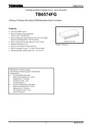
TK10P60W
TK10P60W
TK10P60W

Create successful ePaper yourself
Turn your PDF publications into a flip-book with our unique Google optimized e-Paper software.
MOSFETs Silicon N-Channel MOS (DTMOS)<br />
<strong>TK10P60W</strong><br />
<strong>TK10P60W</strong><br />
1. Applications<br />
• Switching Voltage Regulators<br />
2. Features<br />
(1) Low drain-source on-resistance: RDS(ON) = 0.327 Ω (typ.)<br />
by used to Super Junction Structure : DTMOS<br />
(2) Easy to control Gate switching<br />
(3) Enhancement mode: Vth = 2.7 to 3.7 V (VDS = 10 V, ID = 0.5 mA)<br />
3. Packaging Packaging and Internal Circuit Circuit<br />
DPAK<br />
1<br />
1: Gate<br />
2: Drain (Heatsink)<br />
3: Source<br />
4. Absolute Absolute Maximum Maximum Ratings (Note) (T (Ta = 25 25 unless otherwise specified) specified)<br />
Drain-source voltage<br />
Gate-source voltage<br />
Drain current (DC)<br />
Drain current (pulsed)<br />
Power dissipation<br />
Single-pulse avalanche energy<br />
Avalanche current<br />
Reverse drain current (DC)<br />
Reverse drain current (pulsed)<br />
Channel temperature<br />
Storage temperature<br />
Characteristics<br />
(T c = 25)<br />
(Note 1)<br />
(Note 1)<br />
(Note 2)<br />
(Note 1)<br />
(Note 1)<br />
Symbol<br />
V DSS<br />
V GSS<br />
I D<br />
I DP<br />
P D<br />
E AS<br />
I AR<br />
I DR<br />
I DRP<br />
T ch<br />
T stg<br />
Rating<br />
600<br />
±30<br />
9.7<br />
38.8<br />
80<br />
121<br />
2.5<br />
9.7<br />
38.8<br />
150<br />
-55 to 150<br />
<strong>TK10P60W</strong><br />
Note: Using continuously under heavy loads (e.g. the application of high temperature/current/voltage and the<br />
significant change in temperature, etc.) may cause this product to decrease in the reliability significantly even<br />
if the operating conditions (i.e. operating temperature/current/voltage, etc.) are within the absolute maximum<br />
ratings.<br />
Please design the appropriate reliability upon reviewing the Toshiba Semiconductor Reliability Handbook<br />
("Handling Precautions"/"Derating Concept and Methods") and individual reliability data (i.e. reliability test<br />
report and estimated failure rate, etc).<br />
Unit<br />
V<br />
A<br />
W<br />
mJ<br />
A<br />
<br />
2012-08-27<br />
Rev.2.0
5. Thermal Characteristics<br />
Channel-to-case thermal resistance<br />
Characteristics<br />
Note 1: Ensure that the channel temperature does not exceed 150.<br />
Note 2: VDD = 90 V, Tch = 25 (initial), L = 33.9 mH, RG = 25 Ω, IAR = 2.5 A<br />
2<br />
Symbol<br />
R th(ch-c)<br />
Note: This transistor is sensitive to electrostatic discharge and should be handled with care.<br />
<strong>TK10P60W</strong><br />
Max<br />
1.57<br />
Unit<br />
/W<br />
2012-08-27<br />
Rev.2.0
6. Electrical Electrical Characteristics<br />
6.1. Static Characteristics (T (Taa = 25 25 25 unless otherwise specified)<br />
Characteristics<br />
Gate leakage current<br />
Drain cut-off current<br />
Drain-source breakdown voltage<br />
Gate threshold voltage<br />
Drain-source on-resistance<br />
Symbol<br />
I GSS<br />
I DSS<br />
V (BR)DSS<br />
V th<br />
R DS(ON)<br />
3<br />
Test Condition<br />
V GS = ±30 V, V DS = 0 V<br />
V DS = 600 V, V GS = 0 V<br />
I D = 10 mA, V GS = 0 V<br />
V DS = 10 V, I D = 0.5 mA<br />
V GS = 10 V, I D = 4.9 A<br />
6.2. Dynamic Characteristics (T (Taa = 25 25 unless unless otherwise specified)<br />
Input capacitance<br />
Characteristics<br />
Reverse transfer capacitance<br />
Output capacitance<br />
Effective output capacitance<br />
Gate resistance<br />
Switching time (rise time)<br />
Switching time (turn-on time)<br />
Switching time (fall time)<br />
Switching time (turn-off time)<br />
MOSFET dv/dt ruggedness<br />
Symbol<br />
C iss<br />
C rss<br />
C oss<br />
C o(er)<br />
r g<br />
t r<br />
t on<br />
t f<br />
t off<br />
dv/dt<br />
Test Condition<br />
V DS = 300 V, V GS = 0 V, f = 1 MHz<br />
V DS = 0 to 400 V, V GS = 0 V<br />
V DS = OPEN, f = 1 MHz<br />
See Figure 6.2.1<br />
V DD = 0 to 400 V, I D = 4.9 A<br />
Fig. Fig. 6.2.1 Switching Time Time Test Circuit<br />
6.3. Gate Charge Characteristics (T (Ta = 25 25 unless otherwise specified)<br />
Characteristics<br />
Total gate charge (gate-source plus<br />
gate-drain)<br />
Gate-source charge 1<br />
Gate-drain charge<br />
Symbol<br />
Q g<br />
Q gs1<br />
Q gd<br />
Test Condition<br />
V DD ≈ 400 V, V GS = 10 V, I D = 9.7 A<br />
6.4. Source-Drain Characteristics (T (T (Taa = 25 25 unless otherwise specified)<br />
Characteristics<br />
Diode forward voltage<br />
Reverse recovery time<br />
Reverse recovery charge<br />
Peak reverse recovery current<br />
Diode dv/dt ruggedness<br />
Symbol<br />
V DSF<br />
t rr<br />
Q rr<br />
I rr<br />
dv/dt<br />
Test Condition<br />
I DR = 9.7 A, V GS = 0 V<br />
I DR = 4.9 A, V GS = 0 V<br />
-dI DR/dt = 100 A/µs<br />
I DR = 4.9 A, V GS = 0 V, V DD = 400 V<br />
Min<br />
<br />
<br />
600<br />
2.7<br />
<br />
Min<br />
<br />
<br />
<br />
<br />
<br />
<br />
<br />
<br />
<br />
50<br />
Min<br />
<br />
<br />
<br />
Min<br />
<br />
<br />
<br />
<br />
15<br />
Typ.<br />
<br />
<br />
<br />
<br />
0.327<br />
Typ.<br />
700<br />
2.3<br />
20<br />
35<br />
7.5<br />
22<br />
45<br />
5.5<br />
75<br />
<br />
Typ.<br />
20<br />
4.5<br />
9.5<br />
Typ.<br />
<br />
250<br />
2.2<br />
19<br />
<br />
<strong>TK10P60W</strong><br />
Max<br />
±1<br />
10<br />
<br />
3.7<br />
0.43<br />
Max<br />
<br />
<br />
<br />
<br />
<br />
<br />
<br />
<br />
<br />
<br />
Max<br />
<br />
<br />
<br />
Max<br />
-1.7<br />
<br />
<br />
<br />
<br />
Unit<br />
µA<br />
V<br />
Ω<br />
Unit<br />
pF<br />
Ω<br />
ns<br />
V/ns<br />
Unit<br />
nC<br />
Unit<br />
V<br />
ns<br />
µC<br />
A<br />
V/ns<br />
2012-08-27<br />
Rev.2.0
7. Marking<br />
Fig. 7.1 Marking<br />
4<br />
<strong>TK10P60W</strong><br />
2012-08-27<br />
Rev.2.0
8. Characteristics Curves (Note)<br />
Fig. 8.1 ID - V VVDS<br />
DS<br />
Fig. 8.3 ID - V VVGS<br />
GS<br />
Fig. 8.5 8.5 VDSS DSS - T TTa<br />
5<br />
Fig. 8.2 ID - V VVDS<br />
DS<br />
Fig. 8.4 VDS DS - V V VVGS<br />
GS<br />
Fig. 8.6 RDS(ON) DS(ON) - I IID<br />
<strong>TK10P60W</strong><br />
2012-08-27<br />
Rev.2.0
Fig. 8.7 RDS(ON) DS(ON) - T TTa<br />
Fig. 8.9 C - V VVDS<br />
DS<br />
Fig. 8.11 Vth th - T TTa<br />
6<br />
Fig. 8.8 IDR DR - V VVDS<br />
DS<br />
Fig. 8.10 EOSS OSS - V VVDS<br />
DS<br />
<strong>TK10P60W</strong><br />
Fig. 8.12 Dynamic Input/Output Input/Output Characteristics<br />
2012-08-27<br />
Rev.2.0
Fig. 8.14 EAS AS - T T TTch<br />
ch<br />
(Guaranteed (Guaranteed Maximum)<br />
Fig. 8.16 Test Circuit/Waveform<br />
Fig. 8.13 rth th - t ttw<br />
(Guaranteed (Guaranteed Maximum)<br />
7<br />
Fig. 8.15 PPD - T TTc<br />
(Guaranteed Maximum)<br />
<strong>TK10P60W</strong><br />
2012-08-27<br />
Rev.2.0
Fig. 8.17 Safe Operating Area<br />
(Guaranteed Maximum)<br />
8<br />
<strong>TK10P60W</strong><br />
Note: The above characteristics curves are presented for reference only and not guaranteed by production test,<br />
unless otherwise noted.<br />
2012-08-27<br />
Rev.2.0
Package Dimensions<br />
Weight: 0.36 g (typ.)<br />
TOSHIBA: 2-7K1S<br />
Nickname: DPAK<br />
Package Name(s)<br />
9<br />
<strong>TK10P60W</strong><br />
Unit: mm<br />
2012-08-27<br />
Rev.2.0
RESTRICTIONS ON PRODUCT USE<br />
10<br />
<strong>TK10P60W</strong><br />
• Toshiba Corporation, and its subsidiaries and affiliates (collectively "TOSHIBA"), reserve the right to make changes to the information<br />
in this document, and related hardware, software and systems (collectively "Product") without notice.<br />
• This document and any information herein may not be reproduced without prior written permission from TOSHIBA. Even with TOSHIBA's<br />
written permission, reproduction is permissible only if reproduction is without alteration/omission.<br />
• Though TOSHIBA works continually to improve Product's quality and reliability, Product can malfunction or fail. Customers are responsible<br />
for complying with safety standards and for providing adequate designs and safeguards for their hardware, software and systems which<br />
minimize risk and avoid situations in which a malfunction or failure of Product could cause loss of human life, bodily injury or damage<br />
to property, including data loss or corruption. Before customers use the Product, create designs including the Product, or incorporate<br />
the Product into their own applications, customers must also refer to and comply with (a) the latest versions of all relevant TOSHIBA<br />
information, including without limitation, this document, the specifications, the data sheets and application notes for Product and the<br />
precautions and conditions set forth in the "TOSHIBA Semiconductor Reliability Handbook" and (b) the instructions for the application<br />
with which the Product will be used with or for. Customers are solely responsible for all aspects of their own product design or applications,<br />
including but not limited to (a) determining the appropriateness of the use of this Product in such design or applications; (b) evaluating<br />
and determining the applicability of any information contained in this document, or in charts, diagrams, programs, algorithms, sample<br />
application circuits, or any other referenced documents; and (c) validating all operating parameters for such designs and applications.<br />
TOSHIBA ASSUMES NO LIABILITY FOR CUSTOMERS' PRODUCT DESIGN OR APPLICATIONS.<br />
• PRODUCT IS NEITHER INTENDED NOR WARRANTED FOR USE IN EQUIPMENTS OR SYSTEMS THAT REQUIRE REQUIRE<br />
EXTRAORDINARILY HIGH LEVELS OF OF QUALITY AND/OR RELIABILITY, AND/OR A MALFUNCTION MALFUNCTION OR FAILURE OF WHICH MAY<br />
CAUSE LOSS OF HUMAN LIFE, BODILY INJURY, SERIOUS PROPERTY DAMAGE AND/OR SERIOUS PUBLIC IMPACT<br />
("UNINTENDED USE"). Except for specific applications as expressly stated in this document, Unintended Use includes, without limitation,<br />
equipment used in nuclear facilities, equipment used in the aerospace industry, medical equipment, equipment used for automobiles,<br />
trains, ships and other transportation, traffic signaling equipment, equipment used to control combustions or explosions, safety devices,<br />
elevators and escalators, devices related to electric power, and equipment used in finance-related fields. IF YOU USE USE PRODUCT PRODUCT FOR<br />
UNINTENDED USE, USE, TOSHIBA ASSUMES ASSUMES NO LIABILITY LIABILITY FOR PRODUCT. For details, please contact your TOSHIBA sales<br />
representative.<br />
• Do not disassemble, analyze, reverse-engineer, alter, modify, translate or copy Product, whether in whole or in part.<br />
• Product shall not be used for or incorporated into any products or systems whose manufacture, use, or sale is prohibited under any<br />
applicable laws or regulations.<br />
• The information contained herein is presented only as guidance for Product use. No responsibility is assumed by TOSHIBA for any<br />
infringement of patents or any other intellectual property rights of third parties that may result from the use of Product. No license to any<br />
intellectual property right is granted by this document, whether express or implied, by estoppel or otherwise.<br />
• ABSENT A WRITTEN SIGNED AGREEMENT, AGREEMENT, EXCEPT AS PROVIDED IN THE RELEVANT RELEVANT TERMS AND CONDITIONS OF SALE<br />
FOR PRODUCT, PRODUCT, AND TO THE MAXIMUM EXTENT ALLOWABLE BY LAW, TOSHIBA (1) ASSUMES NO LIABILITY LIABILITY WHATSOEVER,<br />
INCLUDING INCLUDING WITHOUT LIMITATION, INDIRECT, CONSEQUENTIAL, SPECIAL, OR INCIDENTAL DAMAGES OR LOSS, INCLUDING<br />
WITHOUT LIMITATION, LOSS OF PROFITS, LOSS OF OF OPPORTUNITIES, BUSINESS INTERRUPTION AND LOSS OF OF DATA, AND<br />
(2) DISCLAIMS ANY AND ALL ALL EXPRESS OR IMPLIED WARRANTIES AND CONDITIONS RELATED TO SALE, USE OF PRODUCT,<br />
PRODUCT,<br />
OR INFORMATION, INCLUDING WARRANTIES OR CONDITIONS OF MERCHANTABILITY, FITNESS FOR A PARTICULAR<br />
PARTICULAR<br />
PURPOSE, PURPOSE, ACCURACY OF INFORMATION, OR NONINFRINGEMENT.<br />
• Do not use or otherwise make available Product or related software or technology for any military purposes, including without limitation,<br />
for the design, development, use, stockpiling or manufacturing of nuclear, chemical, or biological weapons or missile technology products<br />
(mass destruction weapons). Product and related software and technology may be controlled under the applicable export laws and<br />
regulations including, without limitation, the Japanese Foreign Exchange and Foreign Trade Law and the U.S. Export Administration<br />
Regulations. Export and re-export of Product or related software or technology are strictly prohibited except in compliance with all<br />
applicable export laws and regulations.<br />
• Please contact your TOSHIBA sales representative for details as to environmental matters such as the RoHS compatibility of Product.<br />
Please use Product in compliance with all applicable laws and regulations that regulate the inclusion or use of controlled substances,<br />
including without limitation, the EU RoHS Directive. TOSHIBA TOSHIBA ASSUMES ASSUMES NO LIABILITY FOR DAMAGES OR LOSSES OCCURRING<br />
AS A RESULT OF NONCOMPLIANCE WITH APPLICABLE LAWS AND REGULATIONS.<br />
2012-08-27<br />
Rev.2.0