TMPM330 - Keil
TMPM330 - Keil
TMPM330 - Keil

Create successful ePaper yourself
Turn your PDF publications into a flip-book with our unique Google optimized e-Paper software.
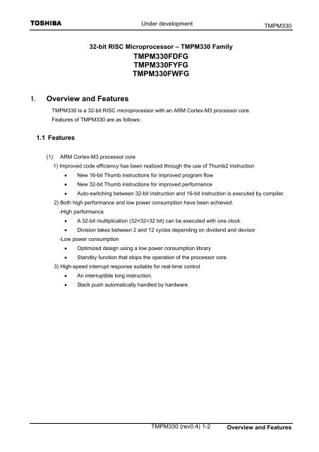
1. Overview and Features<br />
Under development<br />
32-bit RISC Microprocessor – <strong>TMPM330</strong> Family<br />
<strong>TMPM330</strong>FDFG<br />
<strong>TMPM330</strong>FYFG<br />
<strong>TMPM330</strong>FWFG<br />
<strong>TMPM330</strong> is a 32-bit RISC microprocessor with an ARM Cortex-M3 processor core.<br />
Features of <strong>TMPM330</strong> are as follows:<br />
1.1 Features<br />
<strong>TMPM330</strong> (rev0.4) 1-2<br />
<strong>TMPM330</strong><br />
(1) ARM Cortex-M3 processor core<br />
1) Improved code efficiency has been realized through the use of Thumb2 instruction<br />
• New 16-bit Thumb instructions for improved program flow<br />
• New 32-bit Thumb instructions for improved performance<br />
• Auto-switching between 32-bit instruction and 16-bit instruction is executed by compiler.<br />
2) Both high performance and low power consumption have been achieved.<br />
-High performance<br />
• A 32-bit multiplication (32×32=32 bit) can be executed with one clock.<br />
• Division takes between 2 and 12 cycles depending on dividend and devisor<br />
-Low power consumption<br />
• Optimized design using a low power consumption library<br />
• Standby function that stops the operation of the processor core<br />
3) High-speed interrupt response suitable for real-time control<br />
• An interruptible long instruction.<br />
• Stack push automatically handled by hardware.<br />
Overview and Features
(2) On Chip program memory and data memory<br />
Under development<br />
Product name On chip Flash ROM On chip RAM<br />
<strong>TMPM330</strong>FDFG 512Kbyte 32Kbyte<br />
<strong>TMPM330</strong>FYFG 256Kbyte 16Kbyte<br />
<strong>TMPM330</strong>FWFG 128Kbyte 8Kbyte<br />
(3) 16-bit timer : 10 channels<br />
• 16-bit interval timer mode<br />
• 16-bit event counter mode<br />
• 16-bit PPG output<br />
• Input capture function<br />
(4) Real time clock (RTC) : 1 channel<br />
• Clock (hour, minute and second)<br />
• Calendar (Month, week, date and leap year)<br />
• Time correction + or - 30 seconds (by software)<br />
• Alarm (Alarm output)<br />
• Alarm interrupt<br />
(5) Watchdog timer : 1 channel<br />
• 26 cycles of binary counter<br />
• Watchdog timer out<br />
(6) General-purpose serial interface : 3 channels<br />
• Either UART mode or synchronous mode can be selected (4byte FIFO equipped)<br />
(7) Serial bus interface : 3 channels<br />
• Either I2C bus mode or synchronous mode can be selected.<br />
(8) CEC : 1 channel<br />
• Transmission and reception per 1 byte.<br />
(9) Remote control signal preprocessor : 2 channels<br />
• Can receive up to 72bit data at a time<br />
(10) 10-bit A/D converter : 12 channels<br />
• Start by an internal or external timer trigger<br />
• Fixed channel/scan mode<br />
• Single/repeat mode<br />
• AD monitoring 2ch<br />
• Conversion speed 1.44usec(@fsys = 32MHz)<br />
<strong>TMPM330</strong> (rev0.4) 1-3<br />
<strong>TMPM330</strong><br />
(11) Interrupt source<br />
• Internal: 42 factors…The order of precedence can be set over 7 levels (except the watchdog<br />
timer interrupt).<br />
• External: 8 factors…The order of precedence can be set over 7 levels.<br />
(12) Input/ output ports<br />
• 79 pins<br />
Overview and Features
Under development<br />
(13) Standby mode<br />
• Standby modes :IDLE, SLOW, SLEEP, STOP<br />
• Sub clock operation(32.768kHz) :SLOW, SLEEP<br />
(14) Clock generator<br />
• On-chip PLL (quadrupled)<br />
• Clock gear function: The high-speed clock can be divided into 8/8, 4/8, 2/8 or 1/8.<br />
(15) Endian<br />
• Little endian<br />
(16) Maximum operating frequency<br />
• 32MHz<br />
(17) Operating voltage range<br />
• 2.7V~3.6V (with on-chip regulator)<br />
(18) Temperature range<br />
• -20~85 degrees (except during Flash writing/ erasing)<br />
• 0~70 degrees (during Flash writing/ erasing)<br />
(19) Package<br />
• P-LQFP100-P-1414-0.5D (14mm × 14mm, 0.5mm pitch)<br />
<strong>TMPM330</strong> (rev0.4) 1-4<br />
<strong>TMPM330</strong><br />
Overview and Features
1.2 Block Diagram<br />
Cortex-M3<br />
CPU<br />
Debug<br />
NVIC<br />
Under development<br />
Bus Bridge<br />
CG PORT 0~A<br />
SIO (3ch)<br />
I2C (3ch)<br />
CEC<br />
Remote control signal<br />
preprocessor (2ch)<br />
I-Code<br />
D-Code<br />
System<br />
AHB-Bus-Matrix<br />
IO-Bus<br />
I/F<br />
I/F<br />
I/F<br />
Fig. 1.1 <strong>TMPM330</strong> Block Diagram<br />
<strong>TMPM330</strong> (rev0.4) 1-5<br />
FLASH<br />
RAM<br />
BOOT<br />
ROM<br />
TMRB (10ch)<br />
WDT<br />
RTC<br />
ADC (12ch)<br />
<strong>TMPM330</strong><br />
Overview and Features
2. Pin Layout and Pin Functions<br />
Under development<br />
This chapter describes the pin layout, pin names and pin functions of <strong>TMPM330</strong>FDFG/<br />
<strong>TMPM330</strong>FYFG/ <strong>TMPM330</strong>FWFG.<br />
2.1 Pin Layout (Top view)<br />
Fig. 2-1 shows the pin layout of <strong>TMPM330</strong>FDFG/<strong>TMPM330</strong>FYFG/<strong>TMPM330</strong>FWF.<br />
AN10/ PD6<br />
AN11/ PD7<br />
AVSS<br />
VREFH<br />
AVCC<br />
INT4/ PG3<br />
TB9OUT/ PK2<br />
TB7OUT/ PJ5<br />
TB2IN0/ PH4<br />
TB2IN1/ PH5<br />
TB8OUT/ PG7<br />
TEST2<br />
DVSS<br />
DVCC<br />
SDA2/ SO2/ PG4<br />
SCL2/ SI2/ PG5<br />
SCK2/ PG6<br />
TEST1<br />
INT5/ PF7<br />
TXD0/ PE0<br />
RXD0/ PE1<br />
SCLK0/ PE2<br />
TXD1/ PE4<br />
RXD1/ PE5<br />
SCLK1/ PE6<br />
5<br />
10<br />
15<br />
20<br />
25<br />
PD5 /AN9<br />
PD4 /AN8<br />
PD3 /AN7<br />
PD2 /AN6<br />
PD1 /AN5<br />
PD0 /AN4<br />
PC3 /AN3<br />
PC2 /AN2<br />
PC1 /AN1<br />
PC0 /AN0<br />
TEST4<br />
PE3 /RXIN0<br />
PJ4 /TB6OUT<br />
PJ3 /INT3<br />
PJ2 /INT2<br />
PH7 /TB3IN1<br />
PH6 /TB3IN0<br />
PI7 /TB4IN1<br />
RESET<br />
MODE<br />
NMI<br />
PI6 /TB4IN0<br />
XT2<br />
XT1<br />
REGVCC<br />
100<br />
30<br />
95<br />
<strong>TMPM330</strong>FDFG<br />
<strong>TMPM330</strong>FYFG<br />
<strong>TMPM330</strong>FWFG<br />
35<br />
90<br />
Top View<br />
40<br />
85<br />
SDA0/ SO0/ PG0<br />
SCL0/ SI0/ PG1<br />
SCK0/ PG2<br />
PB3<br />
BOOT/ TB0IN0/ PH0<br />
TB0IN1/ PH1<br />
TB1IN0/ PH0<br />
TXD2/ PF0<br />
RXD2/ PF1<br />
SCLK2/ PF2<br />
TB1IN1/ PH3<br />
PB4<br />
TB0OUT/ PI1<br />
INT6/ PJ6<br />
TB1OUT/ PI1<br />
PB5<br />
TB2OUT/ PI2<br />
PB6<br />
SDA1/ SO1/ PF4<br />
SCL1/ SI1/ PF5<br />
SCK1/ PF6<br />
PB7<br />
TB3OUT/ PI3<br />
INT1/ PJ1<br />
CEC/ PK0<br />
Fig. 2.1 Pin Layout (LQFP100)<br />
<strong>TMPM330</strong> (rev0.4) 2-1<br />
45<br />
80<br />
50<br />
75<br />
70<br />
65<br />
60<br />
55<br />
<strong>TMPM330</strong><br />
REGVSS<br />
X1<br />
CVSS<br />
X2<br />
CVCC<br />
PJ0 /INT0<br />
PA7<br />
PA6 /TRACEDATA3<br />
PA5 /TRACEDATA2<br />
PA4 /TRACEDATA1<br />
PA3 /TRACEDATA0<br />
PA2 /TRACECLK<br />
DVSS<br />
DVCC<br />
PF3 /RXIN1<br />
PB2 / TRST<br />
PB1 /TDI<br />
PJ7 /INT7<br />
TEST3<br />
PA1 /TCK /SWCLK<br />
PA0 /TMS /SWDIO<br />
PB0 /TDO /SWV<br />
PI5 /TB5OUT<br />
PI4 /TB4OUT<br />
PK1 /SCOUT<br />
Pin Layout and Pin Functions
Pin<br />
No.<br />
Under development<br />
Table 2.1 Pin Numbers and Names (1/2)<br />
Pin name Pin<br />
No.<br />
1 PD6, AN10 26 PG0, SO0, SDA0<br />
2 PD7, AN11 27 PG1, SI0, SCL0<br />
3 AVSS 28 PG2, SCK0<br />
4 VREFH 29 PB3<br />
5 AVCC 30 PH0, TB0IN0, BOOT<br />
6 PG3, INT4 31 PH1, TB0IN0<br />
7 PK2, TB9OUT 32 PH2, TB1IN0<br />
8 PJ5, TB7OUT 33 PF0, TXD2<br />
9 PH4, TB2IN0 34 PF1, RXD2<br />
10 PH5, TB2IN1 35 PF2, SCLK2<br />
11 PG7, TB8OUT 36 PH3, TB1IN1<br />
12 TEST2 37 PB4<br />
13 DVSS 38 PI0, TB0OUT<br />
14 DVCC 39 PJ6, INT6<br />
15 PG4, SO2, SDA2 40 PI1, TB1OUT<br />
16 PG5, SI2, SCL2 41 PB5<br />
17 PG6, SCK2 42 PI2, TB2OUT<br />
18 TEST1 43 PB6<br />
19 PF7, INT5 44 PF4, SO1, SDA1<br />
20 PE0, TXD0 45 PF5, SI1, SCL1<br />
21 PE1, RXD0 46 PF6, SCK1<br />
22 PE2, SCLK0 47 PB7<br />
23 PE4, TXD1 48 PI3, TB3OUT<br />
24 PE5, RXD1 49 PJ1, INT1<br />
25 PE6, SCLK1 50 PK0, CEC<br />
<strong>TMPM330</strong> (rev0.4) 2-2<br />
Pin name<br />
<strong>TMPM330</strong><br />
Pin Layout and Pin Functions
Pin<br />
No.<br />
Under development<br />
Table 2.1 Pin Numbers and Names (2/2)<br />
Pin name Pin<br />
No.<br />
51 PK1, SCOUT 76 REGVCC<br />
52 PI4, TB4OUT 77 XT1<br />
53 PI5, TB5OUT 78 XT2<br />
54 PB0, TDO, SWV 79 PI6, TB4IN0<br />
55 PA0, TMS, SWDIO 80 NMI<br />
56 PA1, TCK, SWCLK 81 MODE<br />
57 TEST3 82 RESE<br />
58 PJ7, INT7 83 PI7, TB4IN1<br />
59 PB1, TDI 84 PH6, TB3IN0<br />
60 PB2, TRST 85 PH7, TB3IN1<br />
61 PF3, RXIN1 86 PJ2, INT2<br />
62 DVCC 87 PJ3, INT3<br />
63 DVSS 88 PJ4, TB6OUT<br />
64 PA2, TRACECLK 89 PE3, RXIN0<br />
65 PA3, TRACEDATA0 90 TEST4<br />
66 PA4, TRACEDATA1 91 PC0, AN0<br />
67 PA5, TRACEDATA2 92 PC1, AN1<br />
68 PA6, TRACEDATA3 93 PC2, AN2<br />
69 PA7 94 PC3, AN3<br />
70 PJ0, INT0 95 PD0, AN4<br />
71 CVCC 96 PD1, AN5<br />
72 X2 97 PD2, AN6<br />
73 CVSS 98 PD3, AN7<br />
74 X1 99 PD4, AN8<br />
75 REGVSS 100 PD5, AN9<br />
<strong>TMPM330</strong> (rev0.4) 2-3<br />
Pin name<br />
<strong>TMPM330</strong><br />
Pin Layout and Pin Functions
2.2 Pin names and Functions<br />
Under development<br />
<strong>TMPM330</strong> (rev0.4) 2-4<br />
<strong>TMPM330</strong><br />
Table2.2 lists the input and output pins of the <strong>TMPM330</strong>FDFG/<strong>TMPM330</strong>FYFG/<strong>TMPM330</strong>FWFG,<br />
including alternate pin names and functions for multi-function pins.<br />
Type<br />
# of<br />
Pins<br />
Pin Name Input/<br />
Output<br />
Table 2.2 Pin Names and Functions (1/5)<br />
Function<br />
Programma<br />
ble Pull up/<br />
Pull down<br />
Schmitt<br />
trigger<br />
Programm<br />
able Open<br />
Drain<br />
Output<br />
1 PD6<br />
Function<br />
2<br />
AN10<br />
I<br />
I<br />
Input port<br />
Analog input<br />
Pull up - -<br />
PD7<br />
AN11<br />
I<br />
I<br />
Input port<br />
Analog input<br />
A/D converter: GND pin (0V)<br />
Pull up - -<br />
3 AVSS I Connect it to a power supply even if the<br />
A/D converter is not used.<br />
Pin for supplying the A/D converter with<br />
- - -<br />
PS<br />
4 VREFH I<br />
a reference power supply.<br />
Connect this pin to power supply if the<br />
A/D converter is not used.<br />
Pin for supplying the A/D converter with a<br />
- - -<br />
5 AVCC I<br />
power supply. Connect it to a power<br />
supply even if the A/D converter is not<br />
used.<br />
- - -<br />
6 PG3<br />
INT4<br />
I/O<br />
I<br />
I/O port<br />
Interrupt request pin<br />
Pull up<br />
○<br />
w/ noise filter<br />
○<br />
7 PK2<br />
TB9OUT<br />
I/O<br />
O<br />
I/O port<br />
Timer B output<br />
Pull up - -<br />
8 PJ5<br />
TB7OUT<br />
I/O<br />
I<br />
I/O port<br />
Timer B output<br />
Pull up - -<br />
Function<br />
9<br />
PH4<br />
TB2IN0<br />
I/O<br />
I<br />
I/O port<br />
For inputting the capture trigger of timer<br />
B<br />
Pull up ○ -<br />
PH5 I/O I/O port<br />
10 TB2IN1 I Pin for inputting the capture trigger of<br />
timer B<br />
Pull up ○ -<br />
11 PG7<br />
TB8OUT<br />
I/O<br />
O<br />
I/O port<br />
Timer B output<br />
Pull up - ○<br />
Test 12 TEST2 - TEST pin: Set to OPEN. - - -<br />
PS<br />
13<br />
14<br />
DVSS<br />
DVCC<br />
-<br />
-<br />
GND pin<br />
Power supply pin<br />
-<br />
-<br />
-<br />
-<br />
-<br />
-<br />
PG4 I/O I/O port<br />
15<br />
SO2/SD<br />
A2<br />
I/O Pin for sending and receiving data if the<br />
serial bus interface operates in the I2C<br />
mode.<br />
Pull up ○ ○<br />
Function 16<br />
PG5<br />
SI2/SCL<br />
2<br />
I/O<br />
I/O<br />
I/O port<br />
Pin for inputting a clock if the serial bus<br />
interface operates in the I2C mode.<br />
Pull up ○ ○<br />
PG6 I/O I/O port<br />
17<br />
SCK2 I/O Pin for inputting and outputting a clock if<br />
the serial bus interface operates in the<br />
SIO mode.<br />
Pull up ○ ○<br />
Test 18 TEST1 -<br />
TEST pin: Set to OPEN.<br />
- - -<br />
Function 19 PF7<br />
INT5<br />
I/O<br />
I<br />
I/O port<br />
Interrupt request pin<br />
Pull up<br />
○<br />
w/ noise filter<br />
○<br />
Pin Layout and Pin Functions
Type<br />
Function<br />
Function/<br />
BOOT<br />
Function<br />
# of<br />
Pins<br />
Pin Name Input/<br />
Output<br />
Under development<br />
Table 2.2 Pin Names and Functions (2/5)<br />
Function<br />
<strong>TMPM330</strong> (rev0.4) 2-5<br />
Programm<br />
able<br />
Pull-up/<br />
Pull down<br />
Schmitt<br />
trigger<br />
<strong>TMPM330</strong><br />
Programma<br />
ble Open<br />
Drain<br />
Output<br />
20 PE0<br />
TXD0<br />
I/O<br />
O<br />
I/O port<br />
Sending serial data<br />
Pull up - ○<br />
21 PE1<br />
RXD0<br />
I/O<br />
I<br />
I/O port<br />
Receiving serial data<br />
Pull up ○ ○<br />
PE2 I/O I/O port<br />
22 SCLK0 I Serial clock input/ output<br />
Pull up ○ ○<br />
CTS0 I Handshake input pin<br />
24 PE5<br />
RXD1<br />
I/O<br />
I<br />
I/O port<br />
Receiving serial data<br />
Pull up ○ ○<br />
PE6 I/O I/O port<br />
25 SCLK1 I Serial clock input/ output<br />
Pull up ○ ○<br />
CTS1 I Handshake input pin<br />
PG0 I/O I/O port<br />
26<br />
SO0/<br />
SDA0<br />
I/O Pin for sending and receiving data if the<br />
serial bus interface operates in the I2C<br />
mode.<br />
Pull up ○ ○<br />
27<br />
PG1<br />
SI0/<br />
SCL0<br />
I/O<br />
I/O<br />
I/O port<br />
Pin for inputting a clock if the serial bus<br />
interface operates in the I2C mode.<br />
Pull up ○ ○<br />
PG2 I/O I/O port<br />
28<br />
SCK0 I/O Pin for inputting and outputting a clock if<br />
the serial bus interface operates in the<br />
SIO mode.<br />
Pull up ○ ○<br />
29 PB3 I/O I/O port Pull up - -<br />
PH0 I/O I/O port<br />
TB0IN0 I Pin for inputting the capture trigger of<br />
30<br />
BOOT I<br />
timer B<br />
Pin for setting a single boot mode: This<br />
pin goes into single boot mode by<br />
sampling "L" at the rise of a reset signal.<br />
Pull up ○ -<br />
PH1 I/O I/O port<br />
31 TB0IN1 I Pin for inputting the capture trigger of<br />
timer B<br />
Pull up ○ -<br />
PH2 I/O I/O port<br />
32 TB1IN0 I Pin for inputting the capture trigger of<br />
timer B<br />
Pull up ○ -<br />
33 PF0<br />
TXD2<br />
I/O<br />
O<br />
I/O port<br />
Sending serial data<br />
Pull up - ○<br />
34 PF1<br />
RXD2<br />
I/O<br />
I<br />
I/O port<br />
Receiving serial data<br />
Pull up ○ ○<br />
PF2 I/O I/O port<br />
35 SCLK2 I Serial clock input/ output<br />
Pull up ○ ○<br />
CTS2 I Handshake input pin<br />
PH3 I/O I/O port<br />
36 TB1IN1 I Pin for inputting the capture trigger of<br />
timer B<br />
Pull up ○ -<br />
37 PB4 I/O I/O port Pull up - -<br />
38 PI0<br />
TB0OUT<br />
I/O<br />
O<br />
I/O port<br />
Timer B output<br />
Pull up - -<br />
39 PJ6<br />
INT6<br />
I/O<br />
I<br />
I/O port<br />
Interrupt request pin<br />
Pull up<br />
○<br />
w/ noise filter<br />
○<br />
40 PI1<br />
TB1OUT<br />
I/O<br />
O<br />
I/O port<br />
Timer B output<br />
Pull up - -<br />
41 PB5 I/O I/O port Pull up - -<br />
Pin Layout and Pin Functions
Type<br />
# of<br />
Pins<br />
Pin Name Input/<br />
Output<br />
Under development<br />
Table 2.2 Pin Names and Functions (3/5)<br />
Function<br />
<strong>TMPM330</strong> (rev0.4) 2-6<br />
Programmab<br />
le Pull-up/<br />
Pull down<br />
Schmitt<br />
trigger<br />
<strong>TMPM330</strong><br />
Programmab<br />
le Open<br />
Drain<br />
Output<br />
42 PI2<br />
TB2OUT<br />
I/O<br />
O<br />
I/O port<br />
Timer B output<br />
Pull up - -<br />
43 PB6 I/O I/O port Pull up - -<br />
PF4 I/O I/O port<br />
44<br />
SO1/<br />
SDA1<br />
I/O Pin for sending and receiving data if the<br />
serial bus interface operates in the I2C<br />
mode.<br />
Pull up ○ ○<br />
45<br />
PF5<br />
SI1/<br />
SCL1<br />
I/O<br />
I/O<br />
I/O port<br />
Pin for inputting a clock if the serial bus<br />
interface operates in the I2C mode.<br />
Pull up ○ ○<br />
PF6 I/O I/O port<br />
46<br />
SCK1 I/O Pin for inputting and outputting a clock if<br />
the serial bus interface operates in the<br />
Pull up ○ ○<br />
SIO mode.<br />
47 PB7 I/O I/O port Pull up - -<br />
48 PI3<br />
TB3OUT<br />
I/O<br />
O<br />
I/O port<br />
Timer B output<br />
Pull up - -<br />
49 PJ1<br />
INT1<br />
I/O<br />
I<br />
I/O port<br />
Interrupt request pin<br />
Pull up<br />
○<br />
w/ noise filter<br />
○<br />
50 PK0<br />
CEC<br />
I/O<br />
I/O<br />
I/O port<br />
CEC pin<br />
- ○<br />
●<br />
(Note 4)<br />
51 PK1<br />
SCOUT<br />
I/O<br />
O<br />
I/O port<br />
System clock output<br />
Pull up - -<br />
52 PI4<br />
Function<br />
TB4OUT<br />
I/O<br />
O<br />
I/O port<br />
Timer B output<br />
Pull up - -<br />
53 PI5<br />
TB5OUT<br />
I/O<br />
O<br />
I/O port<br />
Timer B output<br />
Pull up - -<br />
54 PB0<br />
TDO/SWV<br />
I/O<br />
O<br />
I/O port<br />
Debug pin<br />
Pull up - -<br />
PA0 I/O I/O port<br />
Function/ 55 TMS/SWDI I/O Debug pin Pull up ○ -<br />
Debug O<br />
PA1 I/O I/O port<br />
56 TCK/<br />
SWCLK<br />
I Debug pin Pull up - -<br />
Test 57 TEST3 - TEST pin: Set to OPEN. - - -<br />
Function 58 PJ7<br />
INT7<br />
I/O<br />
I<br />
I/O port<br />
Interrupt request pin<br />
Pull up<br />
○<br />
w/ noise filter<br />
○<br />
59 PB1<br />
Function/ TDI<br />
I/O<br />
I<br />
I/O port<br />
Debug pin<br />
Pull up - -<br />
Debug<br />
60 PB2<br />
TRST<br />
I/O<br />
I<br />
I/O port<br />
Debug pin<br />
Pull up ○ -<br />
Function 61 PF3<br />
RXIN1<br />
I/O<br />
I<br />
I/O port<br />
Pin for inputting signal to remote controller<br />
Pull up ○ ○<br />
PS<br />
62 DVCC<br />
63 DVSS<br />
-<br />
-<br />
Power supply pin<br />
GND pin<br />
-<br />
-<br />
-<br />
-<br />
-<br />
-<br />
Pin Layout and Pin Functions
Type<br />
Function/<br />
Debug<br />
Function<br />
# of<br />
Pins<br />
Clock 72<br />
Clock 74<br />
Clock<br />
Pin Name Input/<br />
Output<br />
Under development<br />
Table 2.2 Pin Names and Functions (4/5)<br />
Function<br />
<strong>TMPM330</strong> (rev0.4) 2-7<br />
Programma<br />
ble Pull-up/<br />
Pull down<br />
Schmitt<br />
trigger<br />
<strong>TMPM330</strong><br />
Programmab<br />
le Open<br />
Drain<br />
Output<br />
64 PA2<br />
TRACECLK<br />
I/O<br />
O<br />
I/O port<br />
Debug pin<br />
Pull up - -<br />
65 PA3<br />
TRACEDATA0<br />
I/O<br />
O<br />
I/O port<br />
Debug pin<br />
Pull up - -<br />
66 PA4<br />
TRACEDATA1<br />
I/O<br />
O<br />
I/O port<br />
Debug pin<br />
Pull up - -<br />
67 PA5<br />
TRACEDATA2<br />
I/O<br />
O<br />
I/O port<br />
Debug pin<br />
Pull up - -<br />
68 PA6<br />
TRACEDATA3<br />
I/O<br />
O<br />
I/O port<br />
Debug pin<br />
Pull up - -<br />
69 PA7 I/O I/O port Pull up<br />
70 PJ0<br />
INT0<br />
I/O<br />
I<br />
I/O port<br />
Interrupt request pin<br />
Pull up<br />
○<br />
w/ noise filter<br />
○<br />
PS 71 CVCC - Power supply pin - - -<br />
X2 O Pin for connecting a high-speed<br />
oscillator.<br />
- - -<br />
PS 73 CVSS - GND pin - - -<br />
X1 I Pin for connecting a high-speed<br />
oscillator.<br />
- ○ -<br />
PS<br />
75 REGVSS<br />
76 REGVCC<br />
-<br />
-<br />
GND pin<br />
Power supply pin<br />
-<br />
-<br />
-<br />
-<br />
-<br />
-<br />
XT1<br />
77<br />
I Pin for connecting a low-speed<br />
oscillator.<br />
- ○ -<br />
XT2<br />
78<br />
O Pin for connecting a low-speed<br />
oscillator.<br />
- - -<br />
PI6 I/O I/O port<br />
79 TB4IN0 I Pin for inputting the capture trigger of<br />
timer B<br />
Pull up ○ -<br />
80 NMI<br />
I<br />
Non-maskable interrupt<br />
-<br />
○<br />
-<br />
Function<br />
w/ noise filter<br />
Test 81 MODE I Mode pin: Set to DVSS - ○ -<br />
82 RESET<br />
I<br />
Reset input pin Set to<br />
Pull up<br />
○<br />
w/ noise filter<br />
-<br />
PI7 I/O I/O port<br />
83 TB4IN0 I Pin for inputting the capture trigger of<br />
timer B<br />
Pull up ○ -<br />
PH6 I/O I/O port<br />
84 TB3IN0 I Pin for inputting the capture trigger of<br />
timer B<br />
Pull up ○ -<br />
PH7 I/O I/O port<br />
85 TB3IN1 I Pin for inputting the capture trigger of<br />
timer B<br />
Pull up ○ -<br />
86 PJ2<br />
INT2<br />
I/O<br />
I<br />
I/O port<br />
Interrupt request pin<br />
Pull up<br />
○<br />
w/ noise filter<br />
○<br />
87 PJ3<br />
INT3<br />
I/O<br />
I<br />
I/O port<br />
Interrupt request pin<br />
Pull up<br />
○<br />
w/ noise filter<br />
○<br />
88 PJ4<br />
Function<br />
TB6OUT<br />
I/O<br />
O<br />
I/O port<br />
Timer B output<br />
Pull up - -<br />
89 PE3<br />
RXIN0<br />
I/O<br />
I<br />
I/O port<br />
For inputting signal to remote controller<br />
Pull up ○ ○<br />
Test 90 TEST4 - TEST pin: Set to OPEN. - - -<br />
Pin Layout and Pin Functions
Type<br />
Function<br />
# of<br />
Pins<br />
Pin Name<br />
91 PC0<br />
AN0<br />
92 PC1<br />
AN1<br />
93 PC2<br />
AN2<br />
94 PC3<br />
AN3<br />
95 PD0<br />
AN4<br />
96 PD1<br />
AN5<br />
97 PD2<br />
AN6<br />
98 PD3<br />
AN7<br />
99 PD4<br />
AN8<br />
100 PD5<br />
AN9<br />
Input/<br />
Output<br />
I<br />
I<br />
I<br />
I<br />
I<br />
I<br />
I<br />
I<br />
I<br />
I<br />
I<br />
I<br />
I<br />
I<br />
I<br />
I<br />
I<br />
I<br />
I<br />
I<br />
Under development<br />
Table 2.2 Pin Names and Functions (5/5)<br />
Input port<br />
Analog input<br />
Input port<br />
Analog input<br />
Input port<br />
Analog input<br />
Input port<br />
Analog input<br />
Input port<br />
Analog input<br />
Input port<br />
Analog input<br />
Input port<br />
Analog input<br />
Input port<br />
Analog input<br />
Input port<br />
Analog input<br />
Input port<br />
Analog input<br />
Function<br />
<strong>TMPM330</strong> (rev0.4) 2-8<br />
Programma<br />
ble Pull-up/<br />
Pull down<br />
Schmitt<br />
trigger<br />
<strong>TMPM330</strong><br />
Programma<br />
ble Open<br />
Drain<br />
Output<br />
Pull up - -<br />
Pull up - -<br />
Pull up - -<br />
Pull up - -<br />
Pull up - -<br />
Pull up - -<br />
Pull up - -<br />
Pull up - -<br />
Pull up - -<br />
Pull up - -<br />
(Note 1) Be sure to set TEST1 through 4 to OPEN.<br />
(Note 2) Be sure to set MODE pin to DVSS.<br />
(Note 3) VREFH and AVSS pins must be connected to GND pin even if the A/D converter is not used.<br />
(Note 4) Nch open drain port.<br />
Pin Layout and Pin Functions
2.3 Pin Names and Power Supply Pins<br />
Under development<br />
Table 2.3 Pin Names and Power Supplies<br />
Pin name<br />
Power<br />
supply<br />
PA DVCC3<br />
PB DVCC3<br />
PC DVCC3<br />
PD DVCC3<br />
PE DVCC3<br />
PF AVCC3<br />
PG DVCC3<br />
PH DVCC3<br />
PI DVCC3<br />
PJ DVCC3<br />
PK DVCC3<br />
X1, X2 CVCC<br />
XT1, XT2 DVCC3<br />
RESE DVCC3<br />
NMI DVCC3<br />
MODE DVCC3<br />
2.4 Pin Numbers and Power Supply Pins<br />
Table2.4 Pin Numbers and Power Supplies<br />
Power<br />
supply Pin number Voltage range<br />
DVCC 14, 62<br />
AVCC<br />
REGVCC<br />
5<br />
76<br />
2.7V~3.6V<br />
CVCC 71<br />
<strong>TMPM330</strong> (rev0.4) 2-9<br />
<strong>TMPM330</strong><br />
Pin Layout and Pin Functions
3. Processor Core<br />
Under development<br />
<strong>TMPM330</strong> (rev 0.4) 3-1<br />
<strong>TMPM330</strong><br />
The <strong>TMPM330</strong> family has a high-performance 32-bit processor core (ARM Cortex-M3 processor<br />
core). For information on the operations of this processor core, please refer to the “Cortex-M3<br />
Technical Reference Manual”. This chapter describes the functions unique to the <strong>TMPM330</strong> series<br />
that are not explained in that document.<br />
3.1 Reset Operation<br />
3.1.1 Initial state<br />
The internal circuits, register settings and pin status of the <strong>TMPM330</strong> are undefined right after the<br />
power-on. The state continues until the RESET pin receives low level input after all the power supply<br />
voltage is applied.<br />
3.1.2 Operation<br />
As the precondition, ensure that an internal high-frequency oscillator provides stable oscillation<br />
while power supply voltage is in the operating range. To reset the <strong>TMPM330</strong>, input RESET signal at<br />
low level for a minimum duration of 12 system clocks (1.5ms with external 8MHz oscillator).<br />
3.1.3 Cancellation<br />
When the reset is canceled, the system control register and the internal I/O register of the<br />
Cortex-M3 processor core are initialized. Note that the PLL multiplication circuit stops after canceling<br />
the reset. Therefore, set the PLLSEL register to use PLL multiplication circuit once again.<br />
After the reset exception handling is executed, the program branches off to the interrupt service<br />
routine. The address with which the interrupt service routine starts is stored in 0x0000_0004H<br />
(Note 1)<br />
Set the RESET pin to "0" before turning the power on. Cancel the reset after the<br />
power supply voltage has stabilized sufficiently within the operating range.<br />
(Note 2) The reset operation may alter the internal RAM state, but does not alter data in the<br />
backup RAM.
4. Memory map<br />
4.1 Memory map<br />
0x4008 FFFF<br />
0x4000 0000<br />
0x2000 7FFF<br />
0x2000 0000<br />
0x0007 FFFF<br />
0x0000 0000<br />
Under development<br />
Fig. 4-1 shows the memory map of the <strong>TMPM330</strong>FDFG.<br />
Internal IO<br />
Internal RAM (32K)<br />
Internal ROM (512K)<br />
0xFFFF FFFF<br />
0xE010 0000<br />
0xE00F FFFF<br />
0xE004 0000<br />
0xE003 FFFF<br />
0xE000 0000<br />
0xDFFF FFFF<br />
0xA000 0000<br />
0x9FFF FFFF<br />
0x6000 0000<br />
0x5FFF FFFF<br />
0x4000 0000<br />
0x3FFF FFFF<br />
0x2000 0000<br />
0x1FFF FFFF<br />
0x0000 0000<br />
Vendor Specific<br />
Private Peripheral Bus<br />
– External<br />
Private Peripheral Bus<br />
– Internal<br />
External Device<br />
External RAM<br />
Peripheral<br />
SRAM<br />
Code<br />
Fig 4.1 Memory map (<strong>TMPM330</strong>FDFG)<br />
<strong>TMPM330</strong> (rev 0.4) 3-2<br />
Bit Band Alias (32MB)<br />
(31MB)<br />
Bit Band Region (1MB)<br />
Bit Band Alias (32MB)<br />
(31MB)<br />
Bit Band Region (1MB)<br />
<strong>TMPM330</strong><br />
0x43FF FFFF<br />
0x4200 0000<br />
0x41FF FFFF<br />
0x4010 0000<br />
0x4000 0000<br />
0x23FF FFFF<br />
0x2200 0000<br />
0x21FF FFFF<br />
0x2010 0000<br />
0x2000 0000
0x4008 FFFF<br />
0x4000 0000<br />
0x2000 3FFF<br />
0x2000 0000<br />
0x0003 FFFF<br />
0x0000 0000<br />
Under development<br />
Fig. 4-2 shows the memory map of the <strong>TMPM330</strong>FYFG.<br />
Internal IO<br />
Internal RAM (16K)<br />
Internal ROM (256K)<br />
0xFFFF FFFF<br />
0xE010 0000<br />
0xE00F FFFF<br />
0xE004 0000<br />
0xE003 FFFF<br />
0xE000 0000<br />
0xDFFF FFFF<br />
0xA000 0000<br />
0x9FFF FFFF<br />
0x6000 0000<br />
0x5FFF FFFF<br />
0x4000 0000<br />
0x3FFF FFFF<br />
0x2000 0000<br />
0x1FFF FFFF<br />
0x0000 0000<br />
Vendor Specific<br />
Private Peripheral Bus<br />
– External<br />
Private Peripheral Bus<br />
– Internal<br />
External Device<br />
External RAM<br />
Peripheral<br />
SRAM<br />
Code<br />
Fig. 4.2 Memory map (<strong>TMPM330</strong>FYFG)<br />
<strong>TMPM330</strong> (rev 0.4) 3-3<br />
Bit Band Alias (32MB)<br />
(31MB)<br />
Bit Band Region (1MB)<br />
Bit Band Alias (32MB)<br />
(31MB)<br />
Bit Band Region (1MB)<br />
<strong>TMPM330</strong><br />
0x43FF FFFF<br />
0x4200 0000<br />
0x41FF FFFF<br />
0x4010 0000<br />
0x4000 0000<br />
0x23FF FFFF<br />
0x2200 0000<br />
0x21FF FFFF<br />
0x2010 0000<br />
0x2000 0000
0x4008 FFFF<br />
0x4000 0000<br />
0x2000 1FFF<br />
0x2000 0000<br />
0x0001 FFFF<br />
0x0000 0000<br />
Under development<br />
Fig. 4-3 shows the memory map of the <strong>TMPM330</strong>FWFG.<br />
Internal IO<br />
Internal RAM (8K)<br />
Internal ROM (128K)<br />
0xFFFF FFFF<br />
0xE010 0000<br />
0xE00F FFFF<br />
0xE004 0000<br />
0xE003 FFFF<br />
0xE000 0000<br />
0xDFFF FFFF<br />
0xA000 0000<br />
0x9FFF FFFF<br />
0x6000 0000<br />
0x5FFF FFFF<br />
0x4000 0000<br />
0x3FFF FFFF<br />
0x2000 0000<br />
0x1FFF FFFF<br />
0x0000 0000<br />
Vendor Specific<br />
Private Peripheral Bus<br />
– External<br />
Private Peripheral Bus<br />
– Internal<br />
External Device<br />
External RAM<br />
Peripheral<br />
SRAM<br />
Code<br />
Fig. 4.3 Memory map (<strong>TMPM330</strong>FWFG)<br />
<strong>TMPM330</strong> (rev 0.4) 3-4<br />
Bit Band Alias (32MB)<br />
(31MB)<br />
Bit Band Region (1MB)<br />
Bit Band Alias (32MB)<br />
(31MB)<br />
Bit Band Region (1MB)<br />
<strong>TMPM330</strong><br />
0x43FF FFFF<br />
0x4200 0000<br />
0x41FF FFFF<br />
0x4010 0000<br />
0x4000 0000<br />
0x23FF FFFF<br />
0x2200 0000<br />
0x21FF FFFF<br />
0x2010 0000<br />
0x2000 0000
5. Clock/ Mode Control<br />
5.1 Features<br />
Under development<br />
<strong>TMPM330</strong> (rev0.4) 5-1<br />
<strong>TMPM330</strong><br />
The clock/ mode control block enables to select clock gear, prescaler clock and warm-up of the PLL<br />
(including clock multiplication circuit) and oscillator.<br />
The low power consumption mode can reduce power consumption.<br />
5.2 Functions<br />
5.2.1 Modes and Mode Transition<br />
The single clock mode is to use only the high-speed clock. The dual clock mode is to use the<br />
high-speed and low-speed clocks.<br />
The NORMAL mode and the SLOW mode use the high-speed and low-speed clocks for system clock<br />
respectively.<br />
The IDLE, SLEEP and STOP modes can be used as the low power consumption mode that enables to<br />
reduce power consumption by halting processor core operation.<br />
Fig. 5-1 shows diagrams of mode transition.<br />
IDLE mode<br />
(CPU stop)<br />
(I/O selective operation)<br />
Instruction<br />
Interrupt<br />
Instruction<br />
IDLE mode<br />
(CPU stops)<br />
Interrupt<br />
(I/O selective operation)<br />
Instruction<br />
Interrupt<br />
SLEEP mode Instruction<br />
(fs only)<br />
Interrupt<br />
Reset<br />
NORMAL mode<br />
(fc/ gear value)<br />
Reset has been performed.<br />
Instruction<br />
Interrupt<br />
(a) Mode Transition Diagram of Single Clock Mode<br />
Reset<br />
(b) Mode Transition Diagram of Dual Clock Mode<br />
Fig. 5-1 Mode Transition<br />
STOP mode<br />
(Entire circuit stops)<br />
Reset has been performed.<br />
NORMAL mode<br />
(fc/ gear value)<br />
Instruction<br />
Instruction<br />
Interrupt<br />
SLOW mode<br />
Interrupt STOP mode<br />
(fs)<br />
Instruction<br />
(Entire circuit stops)<br />
Clock/ Mode Control
X1<br />
X2<br />
XT1<br />
XT2<br />
5.2.2 Clock System Block Diagram<br />
Fig. 5-2 shows the clock system diagram.<br />
Under development<br />
• High-speed clock gear: fc, fc/2, fc/4, fc/8<br />
• Prescaler clock: fperiph, fperiph/2, fperiph/4, fperiph/8, fperiph/16,fperiph/32<br />
OSCCR0<br />
OSCCR0<br />
OSCCR1<br />
<br />
Starts oscillation<br />
after reset<br />
High-speed<br />
oscillator<br />
Low-speed<br />
oscillator<br />
OSCCR1<br />
<br />
Starts oscillation<br />
after reset.<br />
fperiph<br />
fsys<br />
fs<br />
Warp-up timer<br />
fs<br />
OSCCR0<br />
<br />
PLLSEL<br />
<br />
PLL<br />
fc<br />
fosc<br />
fpll = fosc × 4<br />
OSCCR0<br />
<br />
Stops after releasing reset<br />
1/2 1/4 1/8 1/16 1/32<br />
1/2 1/4 1/8<br />
φT0<br />
SYSCR1<br />
<br />
<strong>TMPM330</strong> (rev0.4) 5-2<br />
SYSCR0<br />
<br />
SYSCR2<br />
<br />
Fig. 5-3 Clock Block Diagram<br />
fsys<br />
fs<br />
<strong>TMPM330</strong><br />
ADC conversion<br />
clock<br />
ADCLK<br />
SYSCR1 <br />
fgear<br />
CKSEL<br />
<br />
SCOUT<br />
fperiph<br />
(To peripheral I/O)<br />
[Peripheral I/O,<br />
prescaler input]<br />
TMRB, SIO, SBI<br />
[AHB-Bus I/O]<br />
CPU, ROM, RAM,<br />
BOOT ROM<br />
[IO-Bus I/O]<br />
TMRB, WDT, RTC,SIO,<br />
SBI, CEC, RMC,<br />
ADC, PORT,<br />
[RTC]<br />
Prescaler input<br />
[CEC, RMC]<br />
Sampling clock<br />
(Note) The input clocks to selector shown with an arrow are set as default after reset.<br />
Clock/ Mode Control
5.3 Registers<br />
5.3.1 Register List<br />
Under development<br />
Table 5-1 shows registers and addresses of the clock generator.<br />
Table 5-1 Registers of Clock Generator<br />
Register name Address<br />
System control register 0 SYSCR0 4004_0200H<br />
System control register 1 SYSCR1 4004_0201H<br />
System control register 2 SYSCR2 4004_0202H<br />
Oscillation control register 0 OSCCR0 4004_0204H<br />
Oscillation control register 1 OSCCR1 4004_0205H<br />
Standby control register 0 STBYCR0 4004_0208H<br />
Standby control register 1 STBYCR1 4004_0209H<br />
Standby control register 2 STBYCR2 4004_020AH<br />
PLL selection register PLLSEL 4004_020CH<br />
System clock selection register CKSEL 4004_0210H<br />
<strong>TMPM330</strong> (rev0.4) 5-3<br />
<strong>TMPM330</strong><br />
Clock/ Mode Control
SYSCR0<br />
SYSCR1<br />
SYSCR2<br />
5.3.2 Detailed Description of Registers<br />
5.3.2.1 System Control Register<br />
Under development<br />
<strong>TMPM330</strong> (rev0.4) 5-4<br />
<strong>TMPM330</strong><br />
7 6 5 4 3 2 1 0<br />
Bit symbol - - - - - GEAR2 GEAR1 GEAR0<br />
Read/Write R R/W R/W R/W<br />
After reset 0 0 0 0 0 0 0 0<br />
Function “0” is read.<br />
High-speed clock (fc) gear<br />
000: fc<br />
001: reserved<br />
010: reserved<br />
011: reserved<br />
100: fc/2<br />
101: fc/4<br />
110: fc/8<br />
111: reserved<br />
15 14 13 12 11 10 9 8<br />
Bit symbol - - - FPSEL - PRCK2 PRCK1 PRCK0<br />
Read/Write R R/W R R/W R/W R/W<br />
After reset 0 0 0 0 0 0 0 0<br />
Function “0” is read. fperiph “0” is read. Prescaler clock<br />
0:fgear<br />
1:fc<br />
000: fperiph<br />
001: fperiph/2<br />
010: fperiph/4<br />
011: fperiph/8<br />
100: fperiph/16<br />
101: fperiph/32<br />
110: Reserved<br />
111: Reserved<br />
23 22 21 20 19 18 17 16<br />
Bit symbol - - - - - -- SCOSEL1 SCOSEL0<br />
Read/Write R R/W R/W<br />
After reset 0 0 0 0 0 0 0 1<br />
Function “0” is read. SCOUT output<br />
00: fs<br />
01: Reserved<br />
10: fsys<br />
11: φT0<br />
31 30 29 28 27 26 25 24<br />
Bit symbol - - - - - - - -<br />
Read/Write R<br />
After reset 0 0 0 0 0 0 0 0<br />
Function “0” is read.<br />
: Specifies the high-speed clock (fc) gear.<br />
: Specifies the prescaler clock to peripheral I/O.<br />
: Specifies the source clock to fperiph.<br />
: Enables to output the specified clock from SCOUT pin.<br />
Clock/ Mode Control
OSCCR<br />
OSCCR<br />
5.3.2.2 Oscillation Control Register<br />
Under development<br />
: Enables to start the warm-up timer.<br />
: Enables to monitor the status of the warm-up timer.<br />
: Specifies operation of the PLL.<br />
It stops after reset. Resetting the bit is required.<br />
: Specifies the oscillator to warm-up.<br />
: Specifies time of the warm-up timer for oscillator.<br />
: Specifies operation of the high-speed oscillator.<br />
: Specifies operation of the low-speed oscillator.<br />
<strong>TMPM330</strong> (rev0.4) 5-5<br />
<strong>TMPM330</strong><br />
7 6 5 4 3 2 1 0<br />
Bit symbol - WUPT2 WUPT1 WUPT0 WUPSEL PLLON WUEF WUEON<br />
Read/Write R R/W R/W R/W R/W R/W R W<br />
After reset 0 0 0 1 0 0 0 0<br />
Function “0” is read. Selection of warm-up time for<br />
oscillator<br />
X1<br />
000: No warm-up<br />
001:2 10 /input freq.<br />
010:2 11 / input freq.<br />
011:2 12 / input freq.<br />
100:2 13 / input freq.<br />
101:2 14 / input freq.<br />
110:2 15 / input freq.<br />
111:2 16 XT1<br />
000:No warm-up<br />
001:2<br />
/ input freq.<br />
6 / input freq.<br />
010:2 7 / input freq.<br />
011:2 8 / input freq.<br />
100:2 15 / input freq.<br />
101:2 16 / input freq.<br />
110:2 17 / input freq.<br />
111:2 18 Warm-up PLL Status of Operation<br />
counter operation Warm-up of warm-up<br />
timer for timer for<br />
0: X1 0: Stop oscillator oscillator<br />
1: XT1 1:<br />
Oscillation 0: warm-up 0: don’t<br />
completed care<br />
1: Warm-up 1: starting<br />
in operation warm-up<br />
/ input freq.<br />
15 14 13 12 11 10 9 8<br />
Bit symbol - - - - - - XTEN XEN<br />
Read/Write R R/W R R/W R/W<br />
After reset 0 0 0 0 0 0 1 1<br />
Function “0” is read. Write “0”. “0” is read. Low-speed High-speed<br />
oscillator oscillator<br />
0: Stop<br />
1:<br />
Oscillation<br />
0: Stop<br />
1:<br />
Oscillation<br />
23 22 21 20 19 18 17 16<br />
Bit symbol - - - - - - - -<br />
Read/Write R<br />
After reset 0 0 0 0 0 0 0 0<br />
Function “0” is read.<br />
31 30 29 28 27 26 25 24<br />
Bit symbol - - - - - - - -<br />
Read/Write R<br />
After reset 0 0 0 0 0 0 0 0<br />
Function “0” is read.<br />
Clock/ Mode Control
STBYCR0<br />
STBYCR1<br />
STBYCR2<br />
5.3.2.3 Standby Control Register<br />
Under development<br />
<strong>TMPM330</strong> (rev0.4) 5-6<br />
<strong>TMPM330</strong><br />
7 6 5 4 3 2 1 0<br />
Bit symbol - - - - - STBY2 STBY1 STBY0<br />
Read/Write R R/W R/W R/W<br />
After reset 0 0 0 0 0 0 1 1<br />
Function “0” is read. Low power consumption mode<br />
15 14 13 12 11<br />
000: Reserved<br />
001: STOP<br />
010: SLEEP<br />
011: IDLE<br />
100: Reserved<br />
101: Reserved<br />
110: Reserved<br />
111: Reserved<br />
10 9 8<br />
Bit symbol - - - - - - RXTEN RXEN<br />
Read/Write R R/W R/W<br />
After reset 0 0 0 0 0 0 0 1<br />
Function “0” is read. Low-speed<br />
oscillator<br />
after<br />
releasing<br />
STOP<br />
mode<br />
0: Stop<br />
1:<br />
Oscillation<br />
High-speed<br />
oscillator<br />
after<br />
releasing<br />
STOP mode<br />
0: Stop<br />
1:<br />
Oscillation<br />
23 22 21 20 19 18 17 16<br />
Bit symbol - - - - - - - DRVE<br />
Read/Write R R/W R/W<br />
After reset 0 0 0 0 0 0 0 0<br />
Function “0” is read. Write “0”. Pin status in<br />
STOP mode<br />
0: Active<br />
1: Inactive<br />
31 30 29 28 27 26 25 24<br />
Bit symbol - - - - - - - -<br />
Read/Write R<br />
After reset 0 0 0 0 0 0 0 0<br />
Function “0” is read.<br />
: Specifies the low power consumption mode.<br />
: Specifies the high-speed oscillator operation after releasing the STOP mode.<br />
: Specifies the low-speed oscillator operation after releasing the STOP mode.<br />
: Specifies the pin status in the STOP mode.<br />
Clock/ Mode Control
PLLSEL<br />
5.3.2.4 PLL Selection Register<br />
Under development<br />
: Specifies use or disuse of the clock multiplied by the PLL.<br />
“X1” is automatically set after reset. Resetting is required when using the PLL.<br />
<strong>TMPM330</strong> (rev0.4) 5-7<br />
<strong>TMPM330</strong><br />
7 6 5 4 3 2 1 0<br />
Bit symbol - - - - - - - PLLSEL<br />
Read/Write R R/W<br />
After reset 0 0 0 0 0 0 0 0<br />
Function “0” is read. Use of PLL<br />
0: Disuse.<br />
X1 selected<br />
1: Use<br />
15 14 13 12 11 10 9 8<br />
Bit symbol - - - - - - - -<br />
Read/Write R<br />
After reset 0 0 0 0 0 0 0 0<br />
Function “0” is read.<br />
23 22 21 20 19 18 17 16<br />
Bit symbol - - - - - - - -<br />
Read/Write R<br />
After reset 0 0 0 0 0 0 0 0<br />
Function “0” is read.<br />
31 30 29 28 27 26 25 24<br />
Bit symbol - - - - - - - -<br />
Read/Write R<br />
After reset 0 0 0 0 0 0 0 0<br />
Function “0” is read.<br />
Clock/ Mode Control
CKSEL<br />
5.3.2.5 System Clock Selection Register<br />
Under development<br />
<strong>TMPM330</strong> (rev0.4) 5-8<br />
<strong>TMPM330</strong><br />
7 6 5 4 3 2 1 0<br />
Bit symbol - - - - - - SYSCK SYSCK<br />
FLG<br />
Read/Write R R/W R<br />
After reset 0 0 0 0 0 0 0 0<br />
Function “0” is read. System<br />
clock<br />
0:<br />
High-speed<br />
(fc)<br />
1:<br />
Low-speed<br />
(fs)<br />
System<br />
clock<br />
status<br />
0:<br />
High-spee<br />
d (fc)<br />
1:<br />
Low-speed<br />
(fs)<br />
Stable<br />
oscillation<br />
identical<br />
with<br />
<br />
value.<br />
15 14 13 12 11 10 9 8<br />
Bit symbol - - - - - - - -<br />
Read/Write R<br />
After reset 0 0 0 0 0 0 0 0<br />
Function “0” is read.<br />
23 22 21 20 19 18 17 16<br />
Bit symbol - - - - - - - -<br />
Read/Write R<br />
After reset 0 0 0 0 0 0 0 0<br />
Function “0” is read.<br />
31 30 29 28 27 26 25 24<br />
Bit symbol - - - - - - - -<br />
Read/Write R<br />
After reset 0 0 0 0 0 0 0 0<br />
Function “0” is read.<br />
: Shows the status of the system clock.<br />
Switching the oscillator with generates time lag to complete. If the<br />
output of the oscillator specified in is read out by , the<br />
switching has been completed.<br />
: Enables to specify the system clock. Setting OSCCR1 and to “1”<br />
in advance is required.<br />
Clock/ Mode Control
5.4 System Clock Control<br />
5.4.1 Initial Values after Reset<br />
Under development<br />
Reset initializes the system clock controller as follows.<br />
High-speed oscillator : ON (oscillating)<br />
Low-speed oscillator : ON (oscillating)<br />
PLL (phase locked loop circuit) : OFF (stop)<br />
High-speed clock gear : fc (no frequency dividing)<br />
<strong>TMPM330</strong> (rev0.4) 5-9<br />
<strong>TMPM330</strong><br />
For example, when a 10-MHz oscillator is connected to the X1 or X2 pin, fsys becomes 10MHz after<br />
reset.<br />
Reset<br />
Reset has been<br />
performed.<br />
NORMAL mode<br />
PLL OFF<br />
fosc = fc = fsys = fperiph<br />
Fig. 5-4 Default State of System Clock<br />
Fosc : Clock frequency to be input via the X1 and X2 pins<br />
Fc : High clock frequency<br />
Fsys : System clock frequency<br />
Fperiph : Clock frequency selected by SYSCR1 (Clock to be input to the peripheral I/O<br />
prescaler)<br />
Clock/ Mode Control
5.4.2 Main System Clock<br />
External<br />
oscillator<br />
Under development<br />
• Allows for oscillator connection or external clock input.<br />
• Clock gear:1/1, 1/2, 1/4, 1/8 (after reset: 1/1)<br />
• High input frequency: 8MHz~10MHz<br />
Min.<br />
operating<br />
freq.<br />
Table 5-2 Range of High-frequency<br />
Max.<br />
operating<br />
freq.<br />
<strong>TMPM330</strong> (rev0.4) 5-10<br />
<strong>TMPM330</strong><br />
After reset Clock gear (CG) Clock gear (CG)<br />
(PLL=OFF, @PLL=ON<br />
@PLL=OFF<br />
CG=1/1) 1/1 1/2 1/4 1/8 1/1 1/2 1/4 1/8<br />
8MHz 8 32 16 8 4 8 4 2 1<br />
1MHz 40MHz<br />
10MHz<br />
10 40 20 10 5 10 5 2.5 1.25<br />
* PLL=ON/OFF setting: available in OSCCR0<br />
Clock gear setting: available in SYSCR0<br />
• Low input frequency<br />
Table 5-3 Range of Low Frequency<br />
Input Frequency Range Maximum Operating<br />
Frequency<br />
Minimum Operating<br />
Frequency<br />
30 ~ 34(kHz) 34 kHz 30 kHz<br />
(Note 1) Switching of clock gear is executed when a value is written to the SYSCR0<br />
register. There are cases where switching does not occur immediately after the change in<br />
the register setting but the original clock gear is used for execution of instructions. If it is<br />
necessary to use the new clock for execution of the instructions following to the clock gear<br />
switching instruction, insert a dummy instruction (to execute a write cycle) and DSB<br />
instruction.<br />
(Note 2) To use the clock gear, ensure that you make the time setting such that φTn of the prescaler<br />
output from each block in the peripheral I/O is calibrated to φTn
Warm-up time options<br />
OSCCR0<br />
Under development<br />
Table 5-4 Warm-up Time (fosc=10 MHz, fs=32.768 kHz)<br />
High-speed clock (fosc)<br />
OSCCR0=“0”<br />
<strong>TMPM330</strong> (rev0.4) 5-11<br />
<strong>TMPM330</strong><br />
Low-speed clock (fs)<br />
OSCCR0=“1”<br />
000 - Without<br />
- Without<br />
warm-up<br />
warm-up<br />
001 2 10 /input frequency 102.4 (μs) 2 6 / input frequency 1.953 (ms)<br />
010 2 11 / input frequency 204.8 (μs) 2 7 / input frequency 3.906 (ms)<br />
011 2 12 / input frequency 409.6 (μs) 2 8 / input frequency 7.813 (ms)<br />
100 2 13 / input frequency 819.2 (μs) 2 15 / input frequency 1.0 (s)<br />
101 2 14 / input frequency 1.638 (ms) 2 16 / input frequency 2.0 (s)<br />
110 2 15 / input frequency 3.277 (ms) 2 17 / input frequency 4.0 (s)<br />
111 2 16 / input frequency 6.554 (ms) 2 18 / input frequency 8.0 (s)<br />
(Note 1) Warm-up is not required when an oscillator module is used for the clock and providing<br />
stable oscillation.<br />
(Note 2) The warm-up timer operates according to the oscillation clock, and it may contain errors<br />
if there is any fluctuation in the oscillation frequency. Therefore, the warm-up time should<br />
be taken as approximate time.<br />
Transition from the NORMAL mode to the SLOW mode<br />
OSCCR0=”xx” : Select the warm-up time<br />
OSCCR1=”1” : Enable the low-speed oscillation (fs)<br />
OSCCR0=”1” : Start the warm-up timer.<br />
OSCCR0Read : Wait until the state becomes "0" (warm-up is finished)<br />
CKSEL=”1” : Switch the system clock to low speed (fs)<br />
CKSEL Read: Confirm that the current state is "1" (the current system clock is fs)<br />
OSCCR1=”0” : Disable the high-speed oscillation (fosc)<br />
Transition from the SLOW mode to the NORMAL mode<br />
OSCCR0=”xx” : Select the warm-up time<br />
OSCCR1=”1” : Enable the high-speed oscillation (fosc)<br />
OSCCR0=”1” : Start the warm-up timer.<br />
OSCCR0 Read : Wait until the state becomes "0" (warm-up is finished).<br />
CKSEL=”0” : Switch the system clock to high speed (fgear)<br />
CKSEL Read: Confirm that the current state is "0" (the current system clock is fgear)<br />
OSCCR1=”0” : Disable the low-speed oscillation (fs)<br />
(Note) When switching the system clock, ensure that the switching has been completed by<br />
reading the SYSCR1.<br />
Clock/ Mode Control
5.4.4 System Clock Pin Output Function<br />
Under development<br />
<strong>TMPM330</strong> (rev0.4) 5-12<br />
<strong>TMPM330</strong><br />
The <strong>TMPM330</strong> enables to output the system clock from a pin. The PK1/SCOUT pin can output the low<br />
speed clock fs, the system clock fsys and the prescaler input clock for peripheral I/O φT0. By setting the<br />
port K registers, the PKCR and PKFR1 to “1”, the PK1/SCOUT pin (pin number 51)<br />
becomes the SCOUT output pin. The output clock is selected by setting the SYSCR3.<br />
SCOUT<br />
selection<br />
SYSCR2<br />
Table 5-5 shows the pin states in each mode when the SCOUT pin is set to the SCOUT output.<br />
Mode<br />
= “00” Output the fs clock.<br />
= “10” Output the fsys clock.<br />
= “11” Output the ΦT0<br />
clock.<br />
Table 5-5 Scout Output State in Each Mode<br />
Low power consumption mode<br />
NORMAL SLOW IDLE SLEEP STOP<br />
(Note) The phase difference (AC timing) between the system clock output by the SCOUT and the<br />
internal clock is not guaranteed.<br />
5.5 Prescaler Clock Control<br />
Each internal I/O (TMRB0-9, SIO0-2 and SBI0-2) has a prescaler for dividing a clock. As the clock φT0<br />
to be input to each prescaler, the "fperiph" clock specified in the SYSCR1 can be divided<br />
according to the setting in the SYSCR1. After the controller is reset, fperiph/1 is selected as<br />
φT0.<br />
5.6 Clock Multiplication Circuit<br />
Fixed to “0” or “1”.<br />
This circuit, which is included in the PLL, outputs the fpll clock that is quadruple of the high-speed<br />
oscillator output clock, fosc. This lowers the oscillator input frequency while increasing the internal clock<br />
speed.<br />
Clock/ Mode Control
5.7 Operation Modes<br />
Under development<br />
<strong>TMPM330</strong> (rev0.4) 5-13<br />
<strong>TMPM330</strong><br />
Two operation modes, NORMAL and SLOW, are available. The features of each mode are described<br />
below.<br />
5.7.1 NORMAL Mode<br />
This mode is to operate the CPU core and the peripheral hardware by using the high-speed clock.<br />
It is shifted to the NORMAL mode after reset. The dual clock operation that uses the low-speed<br />
clock as well is also available.<br />
5.7.2 SLOW Mode<br />
This mode is to operate the CPU core and the peripheral hardware by using the low-speed clock<br />
with high-speed clock stopped. This mode allows the I/O port, real time clock (RTC), CEC and RMC<br />
(remote control signal preprocessor) functions to operate.<br />
(Note) Be sure to stop the peripheral functions except for the CPU, RTC, I/O port, CEC and<br />
RMC before the transition to SLOW mode.<br />
5.8 Low Power Consumption Mode<br />
The <strong>TMPM330</strong> has three low power consumption modes: IDLE, SLEEP and STOP. To shift to the low<br />
power consumption mode, specify the mode in the system control register STBYCR0 and<br />
execute the WFI (Wait For Interrupt) instruction. In this case, execute reset or generate the interrupt to<br />
release the mode. Releasing by the interrupt requires settings in advance. See chapter 6 for details.<br />
(Note) Transition to the low power consumption mode by executing the WFE (Wait For Event)<br />
instruction is prohibited. The <strong>TMPM330</strong> does not offer any event for releasing the low<br />
power consumption mode.<br />
The features of each mode are described below.<br />
Clock/ Mode Control
5.8.1 IDLE Mode<br />
Under development<br />
<strong>TMPM330</strong> (rev0.4) 5-14<br />
<strong>TMPM330</strong><br />
Only the CPU is stopped in this mode.<br />
The internal I/O has one bit of the ON/OFF setting register for operation in the IDLE mode in the<br />
register of each module. This enables operation settings for the IDLE mode. When the internal I/O<br />
has been set not to operate in the IDLE mode, it stops operation and holds the state when the system<br />
enters the IDLE mode.<br />
Table 5-6 shows a list of the IDLE setting registers.<br />
5.8.2 SLEEP Mode<br />
Table 5-6 Internal I/O setting registers for the IDLE mode<br />
Internal I/O IDLE mode setting register<br />
TMRB0~9 TBxRUN<br />
SIO0~2 SCxMOD1<br />
I2C/SIO (SBI0~2) SBIBRx<br />
CEC CECEN<br />
RMC RMCEN<br />
A/D converter ADMOD1<br />
WDT WDMOD<br />
The internal low-speed oscillator, real time clock, CEC (only for reception) and RMC operate. By<br />
releasing the SLEEP mode, the device returns to the preceding mode of the SLEEP mode and starts<br />
operation.<br />
5.8.3 STOP Mode<br />
All the internal circuits including the internal oscillator are brought to a stop.<br />
By releasing the STOP mode, the device returns to the preceding mode of the STOP mode and<br />
starts operation.<br />
The STOP mode enables to select the pin status by setting the STBYCR2. Table 5-7<br />
shows the pin status in the STOP mode.<br />
Clock/ Mode Control
PA<br />
PB<br />
Port<br />
Pin name<br />
Under development<br />
Table 5-7 Pin status of SYSCR2 in STOP mode<br />
Bit<br />
0 (PAFR=0)<br />
(general-purpose port)<br />
0 (PAFR=1)<br />
(TMS/SWDIO)<br />
Input enabled<br />
Output enabled<br />
1-7 Input enabled (PEIE=1)<br />
Output enabled (PECR=1)<br />
0 (PBFR=0)<br />
(general-purpose port)<br />
0 (PBFR=1)<br />
(TDO/SWV)<br />
<strong>TMPM330</strong> (rev0.4) 5-15<br />
Input/ output =0 =1<br />
⎯<br />
⎯<br />
Input<br />
Output<br />
Output enabled (PACR=1) Output Output<br />
Input enabled<br />
Output enabled<br />
⎯<br />
⎯<br />
⎯<br />
⎯<br />
Input<br />
Output<br />
Input<br />
Output<br />
Output enabled (PACR=1) Output Output<br />
1-7 Input enabled (PEIE=1)<br />
⎯<br />
Input<br />
Output enabled (PECR=1)<br />
⎯ Output<br />
PC 0-4 Input enabled (PCIE=1) ⎯ Input<br />
PD 0-7 Input enabled (PDIE=1) ⎯ Input<br />
PE 0-6 Input enabled (PEIE=1)<br />
⎯<br />
Input<br />
Output enabled (PECR=1)<br />
⎯ Output<br />
PF<br />
0-6 Input enabled (PFIE=1)<br />
⎯<br />
Input<br />
Output enabled (PFCR=1)<br />
⎯ Output<br />
7<br />
PFFR=0<br />
(general-purpose port)<br />
PFFR=1<br />
(INT7)<br />
Input enabled (PFIE=1)<br />
Output enabled (PFCR=1)<br />
⎯<br />
⎯<br />
Input<br />
Output<br />
Input enabled (PFIE=1) Input Input<br />
PG<br />
0-2,4-7 Input enabled (PGIE=1)<br />
⎯<br />
Input<br />
Output enabled (PGCR=1)<br />
⎯ Output<br />
3 PGFR=0<br />
Input enabled (PGIE=1)<br />
⎯<br />
Input<br />
(general-purpose port) Output enabled (PGCR=1)<br />
⎯ Output<br />
PGFR=1<br />
(INT4)<br />
Input enabled (PGIE=1) Input Input<br />
PH 0-7 Input enabled (PHIE=1)<br />
⎯<br />
Input<br />
Output enabled (PHCR=1)<br />
⎯ Output<br />
PI 0-7 Input enabled (PIIE=1)<br />
⎯<br />
Input<br />
Output enabled (PICR=1)<br />
⎯ Output<br />
PJ<br />
4-5 Input enabled (PJIE=1)<br />
⎯<br />
Input<br />
Output enabled (PJCR=1)<br />
⎯ Output<br />
0-3,<br />
6,7<br />
PGFR=0<br />
(general-purpose<br />
port)<br />
Input enabled (PJIE=1)<br />
Output enabled (PJCR=1)<br />
⎯<br />
⎯<br />
Input<br />
Output<br />
0-3,<br />
6,7<br />
PGFR=1<br />
(INT0-3,6,7)<br />
Input enabled (PJIE=1)<br />
Input Input<br />
PK 0-2 Input enabled (PKIE=1)<br />
⎯<br />
Input<br />
Output enabled (PKCR=1)<br />
⎯ Output<br />
/RESET Input pin Input Input<br />
/NMI Input pin Input Input<br />
X1, XT1 Input pin ⎯ ⎯<br />
X2, XT2<br />
Output pin<br />
“H” level<br />
Output<br />
“H” level<br />
Output<br />
MODE Input pin Input Input<br />
⎯ : Indicates that the input or output is disabled.<br />
Input: The input gate is active. To prevent the input pin from floating, fix the input voltage to the<br />
"L" or "H" level.<br />
Output: The pin is in the output state.<br />
<strong>TMPM330</strong><br />
Clock/ Mode Control
Under development<br />
5.8.4 Low power Consumption Mode Setting<br />
<strong>TMPM330</strong> (rev0.4) 5-16<br />
<strong>TMPM330</strong><br />
The low power consumption mode is specified by the setting of the standby control register<br />
STBYCR.<br />
Table 5-8 shows the mode setting in the .<br />
Table 5-8 Low power consumption mode setting<br />
Mode<br />
5.8.5 Operational State in Each Mode<br />
STBYCR0<br />
<br />
RESERVED 000<br />
STOP 001<br />
SLEEP 010<br />
IDLE 011<br />
Table 5-9 show the operational state in each mode.<br />
Processor core<br />
I/O port<br />
ADC<br />
SIO<br />
I2C<br />
TMRB<br />
WDT<br />
Table 5-9 Operational State in Each Mode<br />
Block NORMAL SLOW IDLE SLEEP STOP<br />
○<br />
○<br />
○<br />
○<br />
○<br />
○<br />
○<br />
○<br />
○<br />
×<br />
×<br />
×<br />
×<br />
×<br />
×<br />
○<br />
ON/OFF<br />
selectable for<br />
each module<br />
CEC<br />
○<br />
○<br />
○<br />
○<br />
×<br />
RMC<br />
○<br />
○<br />
○<br />
○<br />
×<br />
RTC<br />
○<br />
○<br />
○<br />
○<br />
×<br />
CG ○ ○ ○ ○ ×<br />
PLL ○ × ○ × ×<br />
High-speed oscillator<br />
(fc)<br />
○ *(Note) ○ × ×<br />
Low-speed<br />
(fs)<br />
oscillator ○ ○ ○ ○ ×<br />
○: Operation ×: Stop<br />
(Note) When the system enters the SLOW mode, the high-speed oscillator must be stopped by<br />
setting the OSCCR1.<br />
×<br />
×<br />
×<br />
×<br />
×<br />
×<br />
×<br />
×<br />
×<br />
×<br />
×<br />
×<br />
×<br />
×<br />
Clock/ Mode Control
Under development<br />
5.8.6 Releasing the Low power Consumption Mode<br />
<strong>TMPM330</strong> (rev0.4) 5-17<br />
<strong>TMPM330</strong><br />
The low power consumption mode can be released by an interrupt request or by reset. The<br />
release source that can be used is determined by the low power consumption mode selected.<br />
Details are shown in Table 5-10.<br />
Release<br />
source<br />
Table 5-10 Release Source in Each Mode<br />
IDLE<br />
Low power consumption mode<br />
(programmable)<br />
SLEEP STOP<br />
INTWDT<br />
○<br />
×<br />
×<br />
INT0~7<br />
○<br />
○ (Note 2) ○ (Note 1)<br />
INTRTC<br />
○<br />
○ (Note 2) ×<br />
INTTB0~9<br />
○<br />
×<br />
×<br />
Interrupt INTRX0~2, INTTX0~2<br />
○<br />
×<br />
×<br />
INTSBI0~2<br />
○<br />
×<br />
×<br />
INTCECRX, INTCECTX<br />
○<br />
○ (Note 2) ×<br />
INTRMCRX0,1<br />
○<br />
○ (Note 2) ×<br />
INTAD/INTADHP/ INTADM<br />
○<br />
×<br />
×<br />
RESET ○ ○ ○<br />
○: Starts the interrupt handling after the mode is released. (The reset<br />
initializes the LSI).<br />
×: Unavailable<br />
(Note 1) The standby mode is released after the warm-up time has elapsed.<br />
(Note 2) To return to the NORMAL, release after the warm-up time has elapsed.<br />
(Note 3) To release the low power consumption mode by using the level mode interrupt in<br />
the interruptible state, keep the level until the interrupt handling is started.<br />
Changing the level before then will prevent the interrupt handling from starting<br />
properly.<br />
(Note 4) For shifting to the low power consumption mode, set the CPU to prohibit all the<br />
interrupts other than the release source. If not, releasing may be executed by an<br />
unspecified interrupt.<br />
● Release by interrupt request<br />
To release the low power consumption mode by an interrupt, the CPU must be set in advance to<br />
detect the interrupt. In addition to the setting in the CPU, the clock generator must be set to detect<br />
the interrupt to be used to release the SLEEP and STOP modes.<br />
● Release by reset<br />
Any low power consumption modes can be released by reset.<br />
Note that releasing of the STOP mode requires sufficient reset time to allow the oscillator<br />
operation to become stable. (Time required for stable oscillation + 500μs and more).<br />
Refer to “Chapter 6. Interrupts" for details.<br />
Clock/ Mode Control
5.8.7 Warm-up<br />
Under development<br />
<strong>TMPM330</strong> (rev0.4) 5-18<br />
<strong>TMPM330</strong><br />
When the STOP mode is released, the system clock output is started after the elapse of warm-up<br />
time at the warm-up counter to allow the internal oscillators to stabilize. The same occurs in the<br />
transition to the NORMAL mode after releasing the SLEEP mode.<br />
It is necessary to set the warm-up time in the OSCCR0 before executing the<br />
instruction to enter the STOP/ SLEEP mode.<br />
Table 5-11 shows whether the warm-up setting of each mode transition is required or not.<br />
Table 5-11 Warm-up setting in mode transition<br />
Mode transition Warm-up setting<br />
NORMAL→IDLE Not required<br />
NORMAL→SLEEP Not required<br />
NORMAL→SLOW Not required<br />
NORMAL→STOP Not required<br />
IDLE→NORMAL Not required<br />
SLEEP→NORMAL Auto-warm-up<br />
SLEEP→SLOW Not required<br />
SLOW→NORMAL Required (note)<br />
SLOW→SLEEP Not required<br />
SLOW→STOP Not required<br />
STOP→NORMAL Auto-warm-up<br />
STOP→SLOW Auto-warm-up<br />
(Note) The warm-up must be activated by software.<br />
Clock/ Mode Control
Under development<br />
5.8.8 Clock Operations in Mode Transition<br />
<strong>TMPM330</strong> (rev0.4) 5-19<br />
<strong>TMPM330</strong><br />
The clock operations in mode transition are described in the following sections 5.8.8.1 to 5.8.8.4.<br />
5.8.8.1 Transition of operation modes: NORMAL→STOP→NORMAL<br />
fsys System clock off<br />
(High-speed clock)<br />
Mode<br />
CG<br />
(High-speed clock)<br />
Warm-up<br />
Start of high-speed clock oscillation<br />
Start of warm-up End of warm-up<br />
5.8.8.2 Transition of operation modes: NORMAL→SLEEP→NORMAL<br />
fsys System clock off<br />
(High-speed clock)<br />
Mode<br />
CG<br />
(High-speed clock)<br />
CG<br />
(Low-speed clock) Low-speed clock (fs) continues oscillation.<br />
Start of high-speed clock oscillation<br />
Warm-up<br />
NORMAL STOP<br />
NORMAL<br />
NORMAL SLEEP<br />
NORMAL<br />
Start of warm-up End of warm-up<br />
Clock/ Mode Control
Under development<br />
5.8.8.3 Transition of operation modes: SLOW→STOP→SLOW<br />
fsys System clock off<br />
(Low-speed clock)<br />
Mode<br />
CG<br />
(Low-speed clock)<br />
Warm-up<br />
Start of lowed clock oscillation<br />
Start of warm-up End of warm-up<br />
5.8.8.4 Transition of operation modes: SLOW→SLEEP→SLOW<br />
fsys System clock off<br />
(Low-speed clock)<br />
Mode<br />
CG (fs)<br />
(Low-speed clock)<br />
(Note)<br />
SLOW STOP<br />
SLOW<br />
SLOW SLEEP<br />
SLOW<br />
<strong>TMPM330</strong> (rev0.4) 5-20<br />
<strong>TMPM330</strong><br />
The low-speed clock (fs) continues oscillation. There is no need to make a<br />
warm-up setting.<br />
Clock/ Mode Control
6 Interrupts<br />
Under development<br />
This chapter describes routes, factors and required settings of interrupts.<br />
<strong>TMPM330</strong> (rev0.4) 6-1<br />
<strong>TMPM330</strong><br />
Interrupts have close relation to the CPU core architecture. Refer to “Cortex-M3 Technical Reference<br />
Manual” if needed.<br />
6.1 Overview<br />
The CPU is notified of interrupts by each signal of interrupt factor.<br />
It sets priority on the interrupts and handles an interrupt request with the highest priority.<br />
The CPU is notified of the interrupt factor, which is used for clearing the standby modes, via a clock<br />
generator. Therefore setting of the clock generator is required.<br />
6.2 Interrupt Factors<br />
6.2.1 Interrupt route<br />
External<br />
interrupt<br />
pin<br />
Fig. 6-1 shows an interrupt request route.<br />
Port<br />
Peripheral<br />
IP<br />
Peripheral<br />
IP<br />
Clearing<br />
standby<br />
mode<br />
Clock generator<br />
Fig. 6-1 Interrupt Route<br />
Interrupt request<br />
CPU<br />
Interrupts
6.2.2 Generation<br />
Under development<br />
<strong>TMPM330</strong> (rev0.4) 6-2<br />
<strong>TMPM330</strong><br />
An interrupt signal is sent from an external pin assigned as the interrupt factor or a peripheral IP.<br />
・From external pin<br />
Set the port control register so that the external pin can perform as an interrupt function pin.<br />
・From peripheral IP<br />
6.2.3 Transmission<br />
Set the peripheral IP to make it possible to output the interrupt.<br />
See chapters of relevant IP for details.<br />
An interrupt signal from an external pin or a peripheral IP is directly sent to the CPU unless it is<br />
used to clear the standby mode.<br />
An interrupt that can be used as a factor to clear the standby mode is transmitted to the CPU via<br />
the clock generator. In this case, set the clock generator in advance. An interrupt from an external<br />
pin can be used without setting the clock generator if it does not function as the clearing factor.<br />
Interrupts
6.2.4 List of Interrupt Factors<br />
Under development<br />
Table 6-1 shows the list of interrupt factors.<br />
Table 6-1 List of Hardware Interrupt Factors (1/2)<br />
No. Interrupt Factors<br />
0 INT0 Interrupt pin (PJ0/70pin)<br />
1 INT1 Interrupt pin (PJ1/49pin)<br />
2 INT2 Interrupt pin (PJ2/86pin)<br />
3 INT3 Interrupt pin (PJ3/87pin)<br />
4 INT4 Interrupt pin (PG3/6pin)<br />
5 INT5 Interrupt pin (PF7/19pin)<br />
6 INTRX0 Serial transmit (channel.0)<br />
7 INTTX0 Serial reception (channel.0)<br />
8 INTRX1 Serial transmit (channel.1)<br />
9 INTTX1 Serial reception (channel.1)<br />
10 INTSBI0 Serial bus interface 0<br />
11 INTSBI1 Serial bus interface 1<br />
<strong>TMPM330</strong> (rev0.4) 6-3<br />
Activation trigger<br />
(Clearing standby)<br />
Selectable<br />
<strong>TMPM330</strong><br />
CG interrupt mode<br />
control register<br />
IMCGA<br />
IMCGB<br />
12 INTCECRX CEC reception IMCGB<br />
13 INTCECTX CEC transmission Rising edge<br />
IMCGD<br />
14 INTAINTRMCRX0 Remote control signal reception (channel.0)<br />
IMCGB<br />
15<br />
INTADHP<br />
Highest priority<br />
interrupt<br />
AD conversion complete<br />
16 INTADM0 AD conversion monitoring function interrupt 0<br />
17 INTADM1 AD conversion monitoring function interrupt 1<br />
18 INTTB0 16bit TMRB match detection 0<br />
19 INTTB1 16bit TMRB match detection 1<br />
20 INTTB2 16bit TMRB match detection 2<br />
21 INTTB3 16bit TMRB match detection 3<br />
22 INTTB4 16bit TMRB match detection 4<br />
23 INTTB5 16bit TMRB match detection 5<br />
24 INTTB6 16bit TMRB match detection 6<br />
25 INTRTC Real time clock timer Falling edge IMCGC<br />
26 INTCAP00 16bit TMRB input capture 00<br />
27 INTCAP01 16bit TMRB input capture 01<br />
28 INTCAP10 16bit TMRB input capture 10<br />
29 INTCAP11 16bit TMRB input capture 11<br />
30 INTCAP50 16bit TMRB input capture 50<br />
31 INTCAP51 16bit TMRB input capture 51<br />
32 INTCAP60 16bit TMRB input capture 60<br />
33 INTCAP61 Input capture 61<br />
34<br />
35<br />
INT6<br />
INT7<br />
Interrupt pin (PJ6/39pin)<br />
Interrupt pin (PJ7/58pin)<br />
Selectable IMCGC<br />
36 INTRX2 Serial transmission (channel.2)<br />
37 INTTX2 Serial reception (channel.2)<br />
38 INTSBI2 Serial bus interface 2<br />
39 INTAINTRMCRX1 Remote control signal reception (channel.1) Rising edge IMCGC<br />
40 INTTB7 16bit TMRB match detection 7<br />
41 INTTB8 16bit TMRB match detection 8<br />
42 INTTB9 16bit TMRB match detection 9<br />
Interrupts
Under development<br />
Table 6-1 List of Hardware Interrupt Factors (2/2)<br />
No. Interrupt Factors<br />
43 INTCAP20 16bit TMRB input capture 20<br />
44 INTCAP21 16bit TMRB input capture 21<br />
45 INTCAP30 16bit TMRB input capture 30<br />
46 INTCAP31 16bit TMRB input capture 31<br />
47 INTCAP40 16bit TMRB input capture 40<br />
48 INTCAP41 16bit TMRB input capture 41<br />
49 INTAD A/D conversion completion<br />
6.2.5 Active State<br />
<strong>TMPM330</strong> (rev0.4) 6-4<br />
Activation trigger<br />
(Clearing standby)<br />
Clock<br />
Generator<br />
<strong>TMPM330</strong><br />
The active state indicates which change in signal of an interrupt factor triggers an interrupt. The<br />
CPU considers an interrupt signal as an interrupt factor when it is changed from “L” to “H”. A signal<br />
directly sent from the peripheral IP to the CPU is configured to output the “H” as an interrupt<br />
request.<br />
The active state of the interrupt to clear the standby mode has the options. As for the signal from<br />
the peripheral IP, the trigger is determined to be the rising or falling edges depending on the<br />
interrupt factor. If the signal is from the external pin, the “H” level, “L” level, rising or falling edge is<br />
selectable.<br />
If the interrupt is used for clearing the standby mode, setting the clock generator register is<br />
required. Enable the IMCGx bit and specify the active state in the IMCGx<br />
bits. You must set the activation trigger as shown in Table 6-1.<br />
The interrupt detected by the clock generator is notified to the CPU with a signal in “H” lelvel.<br />
An interrupt from the external pin can be used without setting the clock generator if it does not<br />
function as the clearing factor. However, inputting the “H” pulse or the signal in “H” level is required<br />
so that the CPU can detect it as an interrupt factor.<br />
Interrupts
Not clearing<br />
standby mode<br />
6.3 Interrupt handling<br />
6.3.1 Flowchart<br />
Under development<br />
The following shows how an interrupt is handled.<br />
indicates hardware handling. indicates software handling.<br />
<strong>TMPM330</strong> (rev0.4) 6-5<br />
<strong>TMPM330</strong><br />
Processing Details See<br />
Settings for detection<br />
Settings for sending<br />
interrupt signal<br />
Interrupt factor is<br />
generated<br />
CG detects interrupt<br />
(factor to clear standby<br />
mode)<br />
Clearing standby<br />
mode<br />
Set the CPU register to detect an interrupt.<br />
Set the clock generator as well if the interrupt is made to clear<br />
the standby mode.<br />
○ Common setting<br />
CPU register<br />
○ Setting to clear standby mode<br />
Clock generator<br />
Execute an appropriate setting to send the interrupt signal<br />
depending on the interrupt type.<br />
○ Setting for interrupt from the external pin<br />
Port<br />
○ Setting for interrupt from peripheral IP<br />
Peripheral IP (See chapters of relevant IP for details.)<br />
The interrupt factor is generated.<br />
The interrupt, which is used for clearing the standby modes, is<br />
connected to the CPU via the clock generator.<br />
6.3.2<br />
Preparation<br />
6.3.3<br />
Detection<br />
by CG<br />
Interrupts
Under development<br />
<strong>TMPM330</strong> (rev0.4) 6-6<br />
<strong>TMPM330</strong><br />
Processing Details See<br />
Detecting interrupt<br />
Handling interrupt<br />
Executing interrupt<br />
service routine<br />
Returning to preceding<br />
program<br />
The CPU detects the interrupt.<br />
The interrupt factor with the highest priority is detected<br />
according to the priority order.<br />
The CPU handles the interrupt.<br />
The CPU pushes resister contents to the stack before<br />
entering the interrupt service routine<br />
Program for the interrupt service routine.<br />
Clear the interrupt factor if needed.<br />
Configure to return to the preceding program of the interrupt<br />
service routine.<br />
6.3.4<br />
Detection<br />
by CPU<br />
6.3.5<br />
CPU<br />
processing<br />
6.3.6<br />
Interrupt<br />
service<br />
routine<br />
Interrupts
6.3.2 Preparation<br />
Under development<br />
<strong>TMPM330</strong> (rev0.4) 6-7<br />
<strong>TMPM330</strong><br />
When preparing for an interrupt, you need to pay attention to the order of configuration to avoid<br />
any unexpected interrupt on the way.<br />
Initiating an interrupt or changing its configuration must be implemented in the following order<br />
basically. Disable the interrupt by the CPU. Configure from the farthest route from the CPU. Then<br />
enable the interrupt by the CPU.<br />
To configure the clock generator, you must follow the order indicated here not to cause any<br />
unexpected interrupt. First, configure the precondition. Secondly, clear the data related to the<br />
interrupt in the clock generator and then enable the interrupt.<br />
The following sections are listed in the order of interrupt handling and describe how to configure<br />
them.<br />
(1) Disabling interrupt by CPU<br />
(2) CPU registers setting<br />
(3) Preconfiguration 1 (Interrupt from external pin)<br />
(4) Preconfiguration 2 (interrupt from peripheral IP)<br />
(5) Configuring the clock generator<br />
(6) Enabling interrupt by CPU<br />
(1) Disabling interrupt by CPU<br />
To make the CPU for not accepting any interrupt, write “1” to the corresponding bit of the<br />
Interrupt Clear-Enable register. Each bit of the register, of which default setting is “0” with interrupt<br />
disabled, is assigned to single interrupt factor.<br />
● CPU register<br />
Interrupt Clear-Enable ← “1” (interrupt disabled)<br />
(Note) m: corresponding bit<br />
(2) CPU registers setting<br />
You can assign a priority level from 0 to 255 to an interrupt by writing to the eight bit field in an<br />
Interrupt Priority Register.<br />
Priority level 0 is the highest priority level.<br />
●CPU register<br />
Interrupt Priority ← “priority”<br />
(Note) m: corresponding bit<br />
Interrupts
Under development<br />
<strong>TMPM330</strong> (rev0.4) 6-8<br />
<strong>TMPM330</strong><br />
(3) Preconfiguration 1 (Interrupt from external pin)<br />
Set “1” to the port function register of the corresponding pin. Setting PnFRx[m] allows the pin to<br />
be used as the function pin. Setting PnIE[m] allows the pin to be used as the input port.<br />
● Port register<br />
PnFRx ← “1”<br />
PnIE ← “1”<br />
(Note) n: port number<br />
m: corresponding bit<br />
x: function register number<br />
(4) Preconfiguration 2 (interrupt from peripheral IP)<br />
The setting varies depending on the IP to be used. See chapters of relevant IP for details.<br />
(5) Configuring the clock generator<br />
You need to configure active state and enabling interrupt for an interrupt to clear the standby<br />
mode with the IMCG register of the clock generator. The IMCG register is capable of configuring<br />
each factor.<br />
Before enabling an interrupt, clear the corresponding interrupt request already held. This can<br />
avoid unexpected interrupt. To clear corresponding interrupt request, write value corresponding to<br />
the interrupt to be used to the ICRCG register. See 6.4.6 INTCG Clear Register for each value.<br />
An interrupt from the external pin can be used without setting the clock generator if it does not<br />
function as the clearing factor. However, inputting the “H” pulse or the signal in “H” level is required<br />
so that the CPU can detect it as an interrupt factor.<br />
● Clock generator register<br />
IMCGn ← Active state<br />
ICRCG ← Value corresponding to the interrupt to be used<br />
IMCGn ← “1” (interrupt enabled)<br />
(Note) n: register number<br />
m: number assigned to interrupt factor<br />
Interrupts
Under development<br />
(6) Enabling interrupt by CPU<br />
Enable the interrupt by the CPU as shown below.<br />
<strong>TMPM330</strong> (rev0.4) 6-9<br />
<strong>TMPM330</strong><br />
Clear the suspended interrupt in the Interrupt Clear-Pending register. Enable the intended<br />
interrupt with the Interrupt Set-Enable register. Each bit of the register is assigned to single<br />
interrupt factor.<br />
Writing “1” to the corresponding bit of the Clear-Pending register clears the suspended interrupt.<br />
Writing “1” to the corresponding bit of the Set-Enable register enables the intended interrupt.<br />
●CPU register<br />
Interrupt Clear-Pending ← “1”<br />
Interrupt Set-Enable ← “1”<br />
(Note) m: corresponding bit<br />
6.3.3 Detection by Clock Generator<br />
If the interrupt is used for clearing the standby mode, the interrupt factor is detected by a trigger<br />
for an active state specified in the clock generator, and notified to the CPU.<br />
The interrupt factor that enters active state triggered by a rising or falling edge is held in the clock<br />
generator after detection. However, if a signal in “H” or “L” level is specified as the trigger to enter<br />
the active state, the CPU considers that the interrupt factor is cleared upon exiting from the active<br />
state. Therefore, the active state needs to be kept until the interrupt is detected.<br />
The interrupt detected by the clock generator is notified to the CPU with a signal in “H” level. The<br />
CPU considers the interrupt signal as an interrupt factor when it is changed from “L” to “H”. To<br />
generate an interrupt again, the factor held in the clock generator needs to be cleared with the<br />
INTCG clear register.<br />
6.3.4 Detection by CPU<br />
6.3.5 CPU processing<br />
The CPU detects an interrupt factor with the highest priority.<br />
On detecting the interrupt, the CPU pushes the contents of PC, PSR, r0-r3, r12 and LR to the<br />
stack before entering the interrupt service routine.<br />
Interrupts
6.3.6 Interrupt Service Routine<br />
Under development<br />
<strong>TMPM330</strong> (rev0.4) 6-10<br />
<strong>TMPM330</strong><br />
Interrupt service routine requires specific programming according to the application to be used.<br />
This section describes what is recommended at the service routine programming and how the<br />
factor is cleared.<br />
(1) Pushing during interrupt service routine<br />
Common interrupt service routine is accompanied with the interrupt handling and the pushing of<br />
the register contents. The Cortex-M3 core automatically pushes the contents of PC, PSR, r0-r3,<br />
r12 and LR to the stack. No extra programming is required for them.<br />
Push the contents of other registers if needed.<br />
An interrupt with the higher priority and faults such as NMI are accepted even when the interrupt<br />
service routine is being executed. We recommend you to push the contents of the general purpose<br />
register that might be rewritten.<br />
(2) Clearing interrupt factor<br />
If an interrupt is used for clearing the standby mode, clear the interrupt request with the INTCG<br />
clear register of the clock generator.<br />
If a signal in “H” or “L” level is specified as the trigger to enter the active state, the factor is held<br />
unless it is cleared. In this case, the factor needs to be cleared. Clearing the factor causes clearing<br />
the interrupt request signal from clock generator.<br />
If a rising or falling edge is specified as the trigger to enter the active state, the factor is cleared<br />
by setting the value, which corresponds to the interrupt, to the INTCG clear register. The factor is<br />
detected again when the specified edge appears.<br />
Interrupts
6.4 Interrupt-related registers<br />
Under development<br />
The clock generator registers and their addresses are as shown below.<br />
6.4.1 Registers<br />
● Clock generator registers<br />
ICRCG CG Interrupt Request Clear Register 0x4004_0214<br />
NMIFLG NMI Flag Register 0x4004_0218<br />
RSTFLG Reset Flag Register 0x4004_021C<br />
IMCGA CG Interrupt Mode Control Register A 0x4004_0220<br />
IMCGB CG Interrupt Mode Control Register B 0x4004_0224<br />
IMCGC CG Interrupt Mode Control Register C 0x4004_0228<br />
IMCGD CG Interrupt Mode Control Register D 0x4004_022C<br />
<strong>TMPM330</strong> (rev0.4) 6-11<br />
<strong>TMPM330</strong><br />
Interrupts
6.4.2 CG Interrupt Mode Control Register A<br />
Under development<br />
<strong>TMPM330</strong> (rev0.4) 6-12<br />
<strong>TMPM330</strong><br />
7 6 5 4 3 2 1 0<br />
IMCGA bit Symbol EMCG02 EMCG01 EMCG00 EMST01 EMST00 INT0EN<br />
Read/Write R R/W R R R/W<br />
After reset 0 0 1 0 0 0 0 0<br />
Function<br />
“0” is read. Active state setting of INT0 standby<br />
clear request. (101~111: setting<br />
prohibited)<br />
000: “L” level<br />
001: “H” level<br />
010: Falling edge<br />
011: Rising edge<br />
100: Both edges<br />
Active state of INT0<br />
standby clear request<br />
00: -<br />
01: Rising edge<br />
10: Falling edge<br />
11: Both edges<br />
“0” is read. INT0 clear<br />
input<br />
0: Disable<br />
1: Enable<br />
15 14 13 12 11 10 9 8<br />
bit Symbol EMCG12 EMCG11 EMCG10 EMST11 EMST10 INT1EN<br />
Read/Write R R/W R R R/W<br />
After reset 0 0 1 0 0 0 0 0<br />
Function “0” is read. Active state setting of INT1 standby<br />
clear request. (101~111: setting<br />
prohibited)<br />
Active state of INT1<br />
standby clear request<br />
“0” is read. INT1 clear<br />
input<br />
000: “L” level<br />
001: “H” level<br />
010: Falling edge<br />
011: Rising edge<br />
100: Both edges<br />
00: -<br />
01: Rising edge<br />
10: Falling edge<br />
11: Both edges<br />
0: Disable<br />
1: Enable<br />
23 22 21 20 19 18 17 16<br />
bit Symbol EMCG22 EMCG21 EMCG20 EMST21 EMST20 INT2EN<br />
Read/Write R R/W R R R/W<br />
After reset 0 0 1 0 0 0 0 0<br />
Function “0” is read. Active state setting of INT2 standby<br />
clear request. (101~111: setting<br />
prohibited)<br />
Active state of INT2<br />
standby clear request<br />
“0” is read. INT2 clear<br />
input<br />
000: “L” level<br />
001: “H” level<br />
010: Falling edge<br />
011: Rising edge<br />
100: Both edges<br />
00: -<br />
01: Rising edge<br />
10: Falling edge<br />
11: Both edges<br />
0: Disable<br />
1: Enable<br />
31 30 29 28 27 26 25 24<br />
bit Symbol EMCG32 EMCG31 EMCG30 EMST31 EMST30 INT3EN<br />
Read/Write R R/W R R R/W<br />
After reset 0 0 1 0 0 0 0 0<br />
Function “0” is read. Active state setting of INT3 standby<br />
clear request. (101~111: setting<br />
prohibited)<br />
Active state of INT3<br />
standby clear request<br />
“0” is read. INT3 clear<br />
input<br />
000: “L” level<br />
001: “H” level<br />
010: Falling edge<br />
011: Rising edge<br />
100: Both edges<br />
00: -<br />
01: Rising edge<br />
10: Falling edge<br />
11: Both edges<br />
0: Disable<br />
1: Enable<br />
(Note 1) Refer to EMSTxx bit to know the active condition which is used for clearing<br />
standby.<br />
(Note 2) Please specify the bit for the edge first and then specify the bit for the<br />
. Setting them simultaneously is prohibited.<br />
Interrupts
6.4.3 CG Interrupt Mode Control Register B<br />
Under development<br />
<strong>TMPM330</strong> (rev0.4) 6-13<br />
<strong>TMPM330</strong><br />
7 6 5 4 3 2 1 0<br />
IMCGB bit Symbol EMCG42 EMCG41 EMCG40 EMST41 EMST40 INT4EN<br />
Read/Write R R/W R R R/W<br />
After reset 0 0 1 0 0 0 0 0<br />
Function<br />
“0” is read. Active state setting of INT4 standby<br />
clear request (101~111: setting<br />
prohibited)<br />
000: “L” level<br />
001: “H” level<br />
010: Falling edge<br />
011: Rising edge<br />
100: Both edges<br />
Active state of INT4<br />
standby clear request<br />
00: -<br />
01: Rising edge<br />
10: Falling edge<br />
11: Both edges<br />
“0” is read. INT4 clear<br />
input<br />
0: Disable<br />
1: Enable<br />
15 14 13 12 11 10 9 8<br />
bit Symbol EMCG52 EMCG51 EMCG50 EMST51 EMST50 INT5EN<br />
Read/Write R R/W R R R/W<br />
After reset 0 0 1 0 0 0 0 0<br />
Function “0” is read. Active state setting of INT5 standby<br />
clear request. (101~111: setting<br />
prohibited)<br />
Active state of INT5<br />
standby clear request<br />
“0” is read. INT5 clear<br />
input<br />
000: “L” level<br />
001: “H” level<br />
010: Falling edge<br />
011: Rising edge<br />
100: Both edges<br />
00: -<br />
01: Rising edge<br />
10: Falling edge<br />
11: Both edges<br />
0: Disable<br />
1: Enable<br />
23 22 21 20 19 18 17 16<br />
bit Symbol EMCG62 EMCG61 EMCG60 EMST61 EMST60 INT6EN<br />
Read/Write R R/W R R R/W<br />
After reset 0 0 1 0 0 0 0 0<br />
Function “0” is read. Active state setting of INTCECRX<br />
standby clear request.<br />
Active state of<br />
INTCECRX<br />
“0” is read. INTCEC<br />
RX Clear<br />
standby clear request<br />
input<br />
Set it as shown below.<br />
011: Rising edge<br />
00: -<br />
01: Rising edge<br />
10: Falling edge<br />
11: Both edges<br />
0: Disable<br />
1: Enable<br />
31 30 29 28 27 26 25 24<br />
bit Symbol EMCG72 EMCG71 EMCG70 EMST71 EMST70 INT7EN<br />
Read/Write R R/W R R R/W<br />
After reset 0 0 1 0 0 0 0 0<br />
Function “0” is read. Active state setting of INTRMCRX0<br />
standby clear request.<br />
Active state of<br />
INTRMCRX0 standby<br />
“0” is read. INTRMC<br />
RX0 Clear<br />
clear request<br />
input<br />
Set it as shown below.<br />
011: Rising edge<br />
00: -<br />
01: Rising edge<br />
10: Falling edge<br />
11: Both edges<br />
0: Disable<br />
1: Enable<br />
(Note 1) Refer to EMSTxx bit to know the active condition which is used for clearing<br />
standby.<br />
(Note 2) Please specify the bit for the edge first and then specify the bit for the<br />
. Setting them simultaneously is prohibited.<br />
Interrupts
6.4.4 CG Interrupt Mode Control Register C<br />
Under development<br />
<strong>TMPM330</strong> (rev0.4) 6-14<br />
<strong>TMPM330</strong><br />
7 6 5 4 3 2 1 0<br />
IMCGC bit Symbol EMCG82 EMCG81 EMCG80 EMST81 EMST80 INT8EN<br />
Read/Write R R/W R R R/W<br />
After reset 0 0 1 0 0 0 0 0<br />
Function<br />
“0” is read. Active state setting of INTRTC<br />
standby clear request.<br />
Set it as shown below.<br />
010: Falling edge<br />
Active state of INTRTC<br />
standby clear request.<br />
00: -<br />
01: Rising edge<br />
10: Falling edge<br />
11: Both edges<br />
“0” is read. INTRTC<br />
clear input<br />
0: Disable<br />
1: Enable<br />
15 14 13 12 11 10 9 8<br />
bit Symbol EMCG92 EMCG91 EMCG90 EMST91 EMST90 INT9EN<br />
Read/Write R R/W R R R/W<br />
After reset 0 0 1 0 0 0 0 0<br />
Function “0” is read. Active state setting of INT6 standby Active state of INT6 “0” is read. INT6 clear<br />
clear request. (101~111: setting<br />
prohibited)<br />
standby clear request.<br />
input<br />
000: “L” level<br />
001: “H” level<br />
010: Falling edge<br />
011: Rising edge<br />
100: Both edges<br />
00: -<br />
01: Rising edge<br />
10: Falling edge<br />
11: Both edges<br />
0: Disable<br />
1: Enable<br />
23 22 21 20 19 18 17 16<br />
bit Symbol EMCGA2 EMCGA1 EMCGA0 EMSTA1 EMSTA0 INTAEN<br />
Read/Write R R/W R R R/W<br />
After reset 0 0 1 0 0 0 0 0<br />
Function “0” is read. Active state setting of INT7 standby Active state of INT7 “0” is read. INTA7clear<br />
clear request. (101~111: setting<br />
prohibited)<br />
standby clear request.<br />
input<br />
000: “L” level<br />
001: “H” level<br />
010: Falling edge<br />
011: Rising edge<br />
100: Both edges<br />
00: -<br />
01: Rising edge<br />
10: Falling edge<br />
11: Both edges<br />
0: Disable<br />
1: Enable<br />
31 30 29 28 27 26 25 24<br />
bit Symbol EMCGB2 EMCGB1 EMCGB0 EMSTB1 EMSTB0 INTBEN<br />
Read/Write R R/W R R R/W<br />
After reset 0 0 1 0 0 0 0 0<br />
Function “0” is read. Active state setting of INTRMCRX1 Active state of “0” is read. INTRMC<br />
standby clear request.<br />
INTRMCRX1 standby<br />
RX1 clear<br />
clear request.<br />
input<br />
Set it as shown below.<br />
011: Rising edge<br />
00: -<br />
01: Rising edge<br />
10: Falling edge<br />
11: Both edges<br />
0: Disable<br />
1: Enable<br />
(Note 1) Refer to EMSTxx bit to know the active condition which is used for clearing<br />
standby.<br />
(Note 2) Please specify the bit for the edge first and then specify the bit for the<br />
. Setting them simultaneously is prohibited.<br />
Interrupts
6.4.5 CG Interrupt Mode Control Register D<br />
Under development<br />
<strong>TMPM330</strong> (rev0.4) 6-15<br />
<strong>TMPM330</strong><br />
7 6 5 4 3 2 1 0<br />
IMCGD bit Symbol EMCG82 EMCG81 EMCG80 EMST81 EMST80 INT8EN<br />
Read/Write R R/W R R R/W<br />
After reset 0 0 1 0 0 0 0 0<br />
Function “0” is read. Active state setting of INTCECTX<br />
standby clear request.<br />
“0” is read. INTCECTX<br />
Clear input<br />
Set it as shown below.<br />
010: Falling edge<br />
Active state of<br />
INTCECTX standby<br />
clear request.<br />
00: -<br />
01: Rising edge<br />
10: Falling edge<br />
11: Both edges<br />
0: Disable<br />
1: Enable<br />
15 14 13 12 11 10 9 8<br />
bit Symbol<br />
Read/Write R R/W R R/W<br />
After reset 0 0 1 0 0 0 0 0<br />
Function “0” is read. Write “0”. “0” is read. Write “0”.<br />
23 22 21 20 19 18 17 16<br />
bit Symbol<br />
Read/Write R R/W R R/W<br />
After reset 0 0 1 0 0 0 0 0<br />
Function “0” is read. Write “0”. “0” is read. Write “0”.<br />
31 30 29 28 27 26 25 24<br />
bit Symbol<br />
Read/Write R R/W R R/W<br />
After reset 0 0 1 0 0 0 0 0<br />
Function “0” is read. Write “0”. “0” is read. Write “0”.<br />
(Note 1) Refer to EMSTxx bit to know the active condition which is used for clearing<br />
standby.<br />
(Note 2) Please specify the bit for the edge first and then specify the bit for the<br />
. Setting them simultaneously is prohibited.<br />
Interrupts
Under development<br />
<strong>TMPM330</strong> (rev0.4) 6-16<br />
<strong>TMPM330</strong><br />
Be sure to set active state of the clear request if interrupt is enabled for clearing the STOP/ IDLE /<br />
SLEEP standby modes.<br />
(Note 1) When using interrupts, be sure to follow the sequence of actions shown below:<br />
1) If shared with other general ports, enable the port to receive the interrupt.<br />
2) Set conditions such as active state upon initialization.<br />
3) Clear interrupt requests.<br />
4) Enable interrupts.<br />
(Note 2) Settings must be performed while interrupts are disabled.<br />
(Note 3) For clearing the standby modes with <strong>TMPM330</strong>, 13 interrupt factors (CEC reception/<br />
transmission, remote control signal reception of ch0 and ch1, INT0 to INT7 and RTC timer<br />
interrupt) are available. You can use CG for selecting edge/level of active state and judging<br />
whether the aforementioned factors are to be used for clearing the standby modes.<br />
As for the above interrupt factors excluding INT0 to INT7, set INTxEN bit to “1” and specify<br />
the other related bits to the appropriate active state even when they are not used for clearing<br />
the standby modes.<br />
(Note 4) Among the above 13 factors to be assigned as the standby mode clear request interrupts,<br />
INT0 to INT7 can be used as a normal interrupt without setting CG.<br />
Interrupts
6.4.6 INTCG Clear Register<br />
Under development<br />
<strong>TMPM330</strong> (rev0.4) 6-17<br />
<strong>TMPM330</strong><br />
7 6 5 4 3 2 1 0<br />
ICRCG bit Symbol ICRCG4 ICRCG3 ICRCG2 ICRCG1 ICRCG0<br />
Read/Write R W<br />
After reset 0 0 0 0 0 0<br />
Function “0” is read.<br />
Clear interrupt requests.<br />
0_0000: INT0 0_0100: INT4 0_1000: INTRTC<br />
0_0001: INT1 0_0101: INT5 0_1001: INT6<br />
0_0010: INT2 0_0110:<br />
0_1010: INT7<br />
0_0011: INT3 INTCECRX 0_1011:<br />
0_0111:<br />
IINTRMCRX0<br />
INTRMCRX1<br />
* 0_1100~1_1111: setting prohibited<br />
* ”0” is read.<br />
15 14 13 12 11 10 9 8<br />
bit Symbol<br />
Read/Write R<br />
After reset 0<br />
Function<br />
“0” is read.<br />
bit Symbol<br />
Read/Write<br />
After reset<br />
Function<br />
23 22 21 20 19 18 17 16<br />
“0” is read.<br />
31 30 29 28 27 26 25 24<br />
bit Symbol<br />
Read/Write R<br />
After reset 0<br />
Function<br />
“0” is read.<br />
Interrupts
6.4.7 NMI Flag Register<br />
Under development<br />
<strong>TMPM330</strong> (rev0.4) 6-18<br />
<strong>TMPM330</strong><br />
NMIFLG 7 6 5 4 3 2 1 0<br />
bit Symbol NMIFLG1 NMIFLG0<br />
Read/Write R<br />
After reset 0 0 0 0 0 0 0 0<br />
Function<br />
“0” is read.<br />
NMI factor<br />
generation<br />
flag<br />
0: not<br />
applicable<br />
1:<br />
generated<br />
from NMI<br />
pin<br />
NMI factor<br />
generation<br />
flag<br />
0: not<br />
applicable<br />
1:<br />
generated<br />
from WDT<br />
15 14 13 12 11 10 9 8<br />
bit Symbol<br />
Read/Write R<br />
After reset 0 0 0 0 0 0 0 0<br />
Function<br />
“0” is read.<br />
23 22 21 20 19 18 17 16<br />
bit Symbol<br />
Read/Write R<br />
After reset 0 0 0 0 0 0 0 0<br />
Function<br />
“0” is read.<br />
31 30 29 28 27 26 25 24<br />
bit Symbol<br />
Read/Write R<br />
After reset 0 0 0 0 0 0 0 0<br />
Function<br />
“0” is read.<br />
(Note) are cleared to “0” when they are read.<br />
Interrupts
6.4.8 Reset Flag Register<br />
Under development<br />
<strong>TMPM330</strong> (rev0.4) 6-19<br />
<strong>TMPM330</strong><br />
RSTFLG 7 6 5 4 3 2 1 0<br />
bit Symbol DBGRSTF - WDTRSTF PINRSTF PONRSTF<br />
Read/Write R R/W R/W R/W R/W R/W<br />
After reset 0 0 0 0 0 0 1 1<br />
Function<br />
“0” is read.<br />
Debug reset Write “0”. WDT reset RESET pin Power-on<br />
flag<br />
flag flag reset flag<br />
0: “0” is<br />
written<br />
1: Reset<br />
from<br />
debugger<br />
0: “0” is<br />
written<br />
1: Reset<br />
from<br />
WDT<br />
0: “0” is<br />
written<br />
1: Reset<br />
from<br />
RESET<br />
pin<br />
0: “0” is<br />
written<br />
1: Reset<br />
from<br />
power-on<br />
reset<br />
15 14 13 12 11 10 9 8<br />
bit Symbol<br />
Read/Write R<br />
After reset 0 0 0 0 0 0 0 0<br />
Function<br />
“0” is read.<br />
23 22 21 20 19 18 17 16<br />
bit Symbol<br />
Read/Write R<br />
After reset 0 0 0 0 0 0 0 0<br />
Function<br />
“0” is read.<br />
31 30 29 28 27 26 25 24<br />
bit Symbol<br />
Read/Write R<br />
After reset 0 0 0 0 0 0 0 0<br />
Function<br />
“0” is read.<br />
(Note) The <strong>TMPM330</strong> has power-on reset circuit and this register is initialized only by<br />
power-on reset. Therefore, “1” is set to the bit in initial reset state right<br />
after power-on. Note that this bit is not set by the second and subsequent resets and<br />
this register is not cleared automatically. Write “0” to clear the register.<br />
Interrupts
7 Input/Output Ports<br />
7.1 Port registers<br />
Px : Port register<br />
To read/ write port data.<br />
Under development<br />
PxCR : Control register<br />
To control input/output<br />
* Need to enable the input with PxIE register even when input is set.<br />
PxFRn : Function register<br />
To set functions. An assigned function can be activated by setting “1”.<br />
PxOD : Open drain control register<br />
To switch the input of a register that can be set as programmable open drain.<br />
PxPUP : Pull up control register<br />
To control program pull ups.<br />
<strong>TMPM330</strong><br />
PxIE : Input control enable register<br />
To control inputs. “0” is set as default to avoid through current. This setting prohibits inputs.<br />
<strong>TMPM330</strong>(rev0.4) 7-1<br />
Input/Output Ports
7.1.1 Port A (PA0~PA7)<br />
Under development<br />
<strong>TMPM330</strong><br />
The port A is a general-purpose, 8-bit input/output port. For this port, inputs and outputs can be<br />
specified in units of bits. Besides the general-purpose input/output function, the port A performs the<br />
debug communication function and the debug trace output function.<br />
A reset allows PA0 and PA1 to perform debug communication function and the other bits perform as<br />
the general-purpose port with input/output disabled. When PA0 functions as the TMS or SWDIO port,<br />
input, output and pull-up are enabled. When PA1 functions as the TCK or SWCLK port, input and<br />
pull-down are enabled.<br />
Port A register<br />
7 6 5 4 3 2 1 0<br />
PA Bit Symbol PA7 PA6 PA5 PA4 PA3 PA2 PA1 PA0<br />
(0x4000_0000) Read/Write R/W<br />
After reset “0”<br />
Port A control register<br />
7 6 5 4 3 2 1 0<br />
PACR Bit Symbol PA7C PA6C PA5C PA4C PA3C PA2C PA1C PA0C<br />
(0x4000_0004) Read/Write R/W<br />
After reset 0 0 0 0 0 0 0 1<br />
Function 0: Output disabled 1: Output enabled<br />
Port A function register 1<br />
7 6 5 4 3 2 1 0<br />
PAFR1 Bit Symbol - PA6F1 PA5F1 PA4F1 PA3F1 PA2F1 PA1F1 PA0F1<br />
(0x4000_0008) Read/Write R R/W<br />
After reset 0 0 0 0 0 0 1 1<br />
Function “0” is 0:PORT 0:PORT 0:PORT 0:PORT 0:PORT 0:PORT 0:PORT<br />
read. 1: TRACE 1: TRACE 1: TRACE 1TRACE 1: TRACE 1: TCK/ 1: TMS/<br />
DATA3 DATA2 DATA1 DATA0 CLK SWCLK SWDIO<br />
Port A pull-up control register<br />
7 6 5 4 3 2 1 0<br />
PAPUP Bit Symbol PA7UP PA6UP PA5UP PA4UP PA3UP PA2UP - PA0UP<br />
(0x4000_002C) Read/Write R/W R R/W<br />
After reset 0 0 0 0 0 0 0 1<br />
Function Pull-up Pull-up Pull-up Pull-up Pull-up Pull-up “0” is read. Pull-up<br />
0:off 0:off 0:off 0:off 0:off 0:off<br />
0:off<br />
1:on 1:on 1:on 1:on 1:on 1:on<br />
1:on<br />
Port A pull-down control register<br />
7 6 5 4 3 2 1 0<br />
PAPDN Bit Symbol - - - - - - PA1DN -<br />
(0x4000_0030) Read/Write R R/W R<br />
After reset 0 0 0 0 0 0 1 0<br />
Function “0” is read. Pull-up<br />
0:off<br />
1:on<br />
“0” is read.<br />
<strong>TMPM330</strong>(rev0.4) 7-2<br />
Input/Output Ports
Under development<br />
Port A input enable control register<br />
<strong>TMPM330</strong><br />
7 6 5 4 3 2 1 0<br />
PAIE Bit Symbol PA7IE PA6IE PA5IE PA4IE PA3IE PA2IE PA1IE PA0IE<br />
(0x4000_0038) Read/Write R/W<br />
After reset 0 0 0 0 0 0 1 1<br />
Function Input Input Input Input Input Input Input Input<br />
0:disabled 0:disabled 0:disabled 0:disabled 0:disabled 0:disabled 0:disabled 0:disabled<br />
1:enabled 1:enabled 1:enabled 1:enabled 1:enabled 1:enabled 1:enabled 1:enabled<br />
<strong>TMPM330</strong>(rev0.4) 7-3<br />
Input/Output Ports
7.1.2 Port B (PB0~PB7)<br />
Under development<br />
<strong>TMPM330</strong><br />
The port B is a general-purpose, 8-bit input/output port. For this port, inputs and outputs can be<br />
specified in units of bits. Besides the general-purpose input/output function, the port B performs debug<br />
communication function.<br />
A reset allows PB0, PB1 and PB2 to perform the debug communication function and the other bits<br />
perform as the general-purpose port with input/output disabled. When PB0 functions as the TDO or<br />
SWV port, output is enabled. When PB1 functions as the TDI port, input and pull-up are enabled. When<br />
PB2 functions as the TRST port, input and pull-up are enabled.<br />
Port B register<br />
7 6 5 4 3 2 1 0<br />
PB Bit Symbol PB7 PB6 PB5 PB4 PB3 PB2 PB1 PB0<br />
(0x4000_0040) Read/Write R/W<br />
After reset “0”<br />
Port B control register<br />
7 6 5 4 3 2 1 0<br />
PBCR Bit Symbol PB7C PB6C PB5C PB4C PB3C PB2C PB1C PB0C<br />
(0x4000_0044) Read/Write R/W<br />
After reset 0 0 0 0 0 0 0 1<br />
Function 0: Output disabled 1: Output enabled<br />
Port B function register 1<br />
7 6 5 4 3 2 1 0<br />
PBFR1 Bit Symbol - - - - - PB2F1 PB1F1 PB0F1<br />
(0x4000_0048) Read/Write R R/W<br />
After reset 0 1 1 1<br />
Function “0” is read. 0:PORT 0:PORT 0:PORT<br />
1: TRST 1: TDI 1:<br />
TDO/SWV<br />
Port B pull-up control register<br />
7 6 5 4 3 2 1 0<br />
PBPUP Bit Symbol PB7UP PB6UP PB5UP PB4UP PB3UP PB2UP PB1UP PB0UP<br />
(0x4000_006C) Read/Write R/W<br />
After reset 0 0 0 0 0 1 1 0<br />
Function Pull-up Pull-up Pull-up Pull-up Pull-up Pull-up Pull-up Pull-up<br />
0:off 0:off 0:off 0:off 0:off 0:off 0:off 0:off<br />
1:on 1:on 1:on 1:on 1:on 1:on 1:on 1:on<br />
Port B input enable control register<br />
7 6 5 4 3 2 1 0<br />
PBIE Bit Symbol PB7IE PB6IE PB5IE PB4IE PB3IE PB2IE PB1IE PB0IE<br />
(0x4000_0078) Read/Write R/W<br />
After reset 0 0 0 0 0 1 1 0<br />
Function Input Input Input Input Input Input Input Input<br />
0:disabled 0:disabled 0:disabled 0:disabled 0:disabled 0:disabled 0:disabled 0:disabled<br />
1:enabled 1:enabled 1:enabled 1:enabled 1:enabled 1:enabled 1:enabled 1:enabled<br />
<strong>TMPM330</strong>(rev0.4) 7-4<br />
Input/Output Ports
7.1.3 Port C (PC0~PC3)<br />
Under development<br />
<strong>TMPM330</strong><br />
The port C is a 4-bit input port. Besides the general-purpose input function, the port C functions as the<br />
analog input port of the A/D converter.<br />
A reset allows all bits to perform as the general-purpose input port and the port C to be put in input<br />
disable mode.<br />
Set the input enable control register when you use the port C as an input port. The setting is not<br />
required when you use it as an analog input port of the A/D converter.<br />
Port C register<br />
7 6 5 4 3 2 1 0<br />
PC Bit Symbol - - - - PC3 PC2 PC1 PC0<br />
(0x4000_0080) Read/Write R R/W<br />
After reset “0” is read. “0”<br />
Port C pull-up control register<br />
7 6 5 4 3 2 1 0<br />
PCPUP Bit Symbol - - - - PC3UP PC2UP PC1UP PC0UP<br />
(0x4000_00AC) Read/Write R R/W<br />
After reset 0 0 0 0 0<br />
Function “0” is read. Pull-up Pull-up Pull-up Pull-up<br />
0:off 0:off 0:off 0:off<br />
1:on 1:on 1:on 1:on<br />
Port C input enable control register<br />
7 6 5 4 3 2 1 0<br />
PCIE Bit Symbol - - - - PC3IE PC2IE PC1IE PC0IE<br />
(0x4000_00B8) Read/Write R R/W<br />
After reset 0 0 1 1 0<br />
Function “0” is read. Input Input Input Input<br />
0:disabled 0:disabled 0:disabled 0:disabled<br />
1:enabled 1:enabled 1:enabled 1:enabled<br />
<strong>TMPM330</strong>(rev0.4) 7-5<br />
Input/Output Ports
7.1.4 Port D (PD0~PD7)<br />
Under development<br />
<strong>TMPM330</strong><br />
The port D is an 8-bit input port. Besides the general-purpose input function, the port D receives an<br />
analog input of the A/D converter and a 16-bit timer input.<br />
A reset allows all bits to perform as the general-purpose input port and the port D to be put in input<br />
disable mode.<br />
Set the input enable control register when you use the port D as an input port. Set the function register<br />
1 and input enable control register when you use the port D as an input port of the 16-bit timer. The<br />
setting is not required when you use it as an analog input port of the A/D converter.<br />
Port D register<br />
7 6 5 4 3 2 1 0<br />
PD Bit Symbol PD7 PD6 PD5 PD4 PD3 PD2 PD1 PD0<br />
(0x4000_00C0) Read/Write R/W<br />
After reset “0”<br />
Port D function register 1<br />
7 6 5 4 3 2 1 0<br />
PDFR1 Bit Symbol - - - - PD3F1 PD2F1 PD1F1 PD0F1<br />
(0x4000_00C8) Read/Write R R/W<br />
After reset 0 0 0 0 0<br />
Function “0” is read. 0:PORT 0:PORT 0:PORT 0:PORT<br />
1: TB6IN1 1: TB6IN0 1: TB5IN1 1: TB5IN0<br />
Port D pull-up control register<br />
7 6 5 4 3 2 1 0<br />
PDPUP Bit Symbol PD7UP PD6UP PD5UP PD4UP PD3UP PD2UP PD1UP PD0UP<br />
(0x4000_00EC) Read/Write R/W<br />
After reset 0 0 0 0 0 0 0 0<br />
Function Pull-up Pull-up Pull-up Pull-up Pull-up Pull-up Pull-up Pull-up<br />
0:off 0:off 0:off 0:off 0:off 0:off 0:off 0:off<br />
1:on 1:on 1:on 1:on 1:on 1:on 1:on 1:on<br />
Port D input enable control register<br />
7 6 5 4 3 2 1 0<br />
PDIE Bit Symbol PD7IE PD6IE PD5IE PD4IE PD3IE PD2IE PD1IE PD0IE<br />
(0x4000_00F8) Read/Write R/W<br />
After reset 0 0 0 0 0 0 0 0<br />
Function Input Input Input Input Input Input Input Input<br />
0:disabled 0:disabled 0:disabled 0:disabled 0:disabled 0:disabled 0:disabled 0:disabled<br />
1:enabled 1:enabled 1:enabled 1:enabled 1:enabled 1:enabled 1:enabled 1:enabled<br />
<strong>TMPM330</strong>(rev0.4) 7-6<br />
Input/Output Ports
7.1.5 Port E (PE0~PE6)<br />
Under development<br />
<strong>TMPM330</strong><br />
The port E is a general-purpose, 7-bit input/output port. For this port, inputs and outputs can be<br />
specified in units of bits. Besides the general-purpose port function, the port E performs the serial<br />
interface function and the remote control signal preprocessor input function.<br />
A reset allows all bits to perform as the general-purpose port and the port E to be put in input/ output<br />
disable mode.<br />
Port E register<br />
7 6 5 4 3 2 1 0<br />
PE Bit Symbol - PE6 PE5 PE4 PE3 PE2 PE1 PE0<br />
(0x4000_0100) Read/Write R R/W<br />
After reset “0” “0”<br />
Port E control register<br />
7 6 5 4 3 2 1 0<br />
PECR Bit Symbol - PE6C PE5C PE4C PE3C PE2C PE1C PE0C<br />
(0x4000_0104) Read/Write R R/W<br />
After reset 0 0 0 0 0 0 0 0<br />
Function “0” is read. 0: Output disabled 1: Output enabled<br />
Port E function register 1<br />
7 6 5 4 3 2 1 0<br />
PEFR1 Bit Symbol - PE6F1 PE5F1 PE4F1 PE3F1 PE2F1 PE1F1 PE0F1<br />
(0x4000_0108) Read/Write R R/W<br />
After reset 0 0 0 0 0 0 0 0<br />
Function “0” is read. 0:PORT 0:PORT 0:PORT 0:PORT 0:PORT 0:PORT 0:PORT<br />
1:SCLK1 1:RXD1 1: TXD1 1:RXIN0 1:SCLK0 1:RXD0 1: TXD0<br />
Port E function register 2<br />
7 6 5 4 3 2 1 0<br />
PEFR2 Bit Symbol - PE6F2 - - - PE2F2 - -<br />
(0x4000_010C) Read/Write R R/W R R/W R<br />
After reset 0 0 0 0 0<br />
Function “0” is read. 0:PORT<br />
“0” is read. 0:PORT “0” is read.<br />
1:CTS1<br />
1:CTS0<br />
Port E open drain control register<br />
7 6 5 4 3 2 1 0<br />
PEOD Bit Symbol - PE6OD PE5OD PE4OD PE3OD PE2OD PE1OD PE0OD<br />
(0x4000_ 0128) Read/Write R R/W R/W R/W R/W R/W R/W R/W<br />
After reset 0 0 0 0 0 0 0 0<br />
Function “0” is read. 0:CMOS 0:CMOS 0:CMOS 0:CMOS 0:CMOS 0:CMOS 0:CMOS<br />
1:Open 1:Open 1:Open 1:Open 1:Open 1:Open 1:Open<br />
drain drain drain drain drain drain drain<br />
<strong>TMPM330</strong>(rev0.4) 7-7<br />
Input/Output Ports
Under development<br />
Port E pull-up control register<br />
<strong>TMPM330</strong><br />
7 6 5 4 3 2 1 0<br />
PEPUP Bit Symbol - PE6UP PE5UP PE4UP PE3UP PE2UP PE1UP PE0UP<br />
(0x4000_012C) Read/Write R R/W<br />
After reset 0 0 0 0 0 0 0 0<br />
Function “0” is Pull-up Pull-up Pull-up Pull-up Pull-up Pull-up Pull-up<br />
read. 0:off 0:off 0:off 0:off 0:off 0:off 0:off<br />
1:on 1:on 1:on 1:on 1:on 1:on 1:on<br />
Port E input enable control register<br />
7 6 5 4 3 2 1 0<br />
PEIE Bit Symbol - PE6IE PE5IE PE4IE PE3IE PE2IE PE1IE PE0IE<br />
(0x4000_0138) Read/Write R R/W<br />
After reset 0 0 0 0 0 0 0 0<br />
Function “0” is read. Input Input Input Input Input Input Input<br />
0:disabled 0:disabled 0:disabled 0:disabled 0:disabled 0:disabled 0:disabled<br />
1:enabled 1:enabled 1:enabled 1:enabled 1:enabled 1:enabled 1:enabled<br />
<strong>TMPM330</strong>(rev0.4) 7-8<br />
Input/Output Ports
7.1.6 Port F (PF0~PF7)<br />
Under development<br />
<strong>TMPM330</strong><br />
The port F is a general-purpose, 8-bit input/output port. For this port, inputs and outputs can be<br />
specified in units of bits. Besides the general-purpose port function, the port F performs the functions of<br />
the serial interface, the remote control signal preprocessor, the serial bus interface and the external<br />
interrupt input.<br />
A reset allows all bits to perform as the general-purpose port and the port F to be put in input/ output<br />
disable mode.<br />
Port F register<br />
7 6 5 4 3 2 1 0<br />
PF Bit Symbol PF7 PF6 PF5 PF4 PF3 PF2 PF1 PF0<br />
(0x4000_0140) Read/Write R/W<br />
After reset “0”<br />
Port F control register<br />
7 6 5 4 3 2 1 0<br />
PFCR Bit Symbol PF7C PF6C PF5C PF4C PF3C PF2C PF1C PF0C<br />
(0x4000_0144) Read/Write R/W<br />
After reset 0 0 0 0 0 0 0 0<br />
Function 0: Output disabled 1: Output enabled<br />
Port F function register 1<br />
7 6 5 4 3 2 1 0<br />
PFFR1 Bit Symbol PF7F1 PF6F1 PF5F1 PF4F1 PF3F1 PF2F1 PF1F1 PF0F1<br />
(0x4000_0148) Read/Write R/W<br />
After reset 0 0 0 0 0 0 0 0<br />
Function 0:PORT 0:PORT 0:PORT 0:PORT 0:PORT 0:PORT 0:PORT 0:PORT<br />
1: INT5 1: SCK1 1: SI1/ 1: SO1/ 1: RXIN1 1: SCLK2 1: RXD2 1: TXD2<br />
SCL1 SDA1<br />
Port F function register 2<br />
7 6 5 4 3 2 1 0<br />
PFFR2 Bit Symbol - - - - - PF2F2 - -<br />
(0x4000_014C) Read/Write R R/W R<br />
After reset 0 0 0<br />
Function “0” is read. 0:PORT<br />
1:CTS2<br />
“0” is read.<br />
Port F open drain control register<br />
7 6 5 4 3 2 1 0<br />
PFOD Bit Symbol PF7OD PF6OD PF5OD PF4OD PF3OD PF2OD PF1OD PF0OD<br />
(0x4000_0168) Read/Write R/W R/W R/W R/W R/W R/W R/W R/W<br />
After reset 0 0 0 0 0 0 0 0<br />
Function 0:CMOS 0:CMOS 0:CMOS 0:CMOS 0:CMOS 0:CMOS 0:CMOS 0:CMOS<br />
1:Open 1:Open 1:Open 1:Open 1:Open 1:Open 1:Open 1:Open<br />
drain drain drain drain drain drain drain drain<br />
<strong>TMPM330</strong>(rev0.4) 7-9<br />
Input/Output Ports
Under development<br />
Port F pull-up control register<br />
<strong>TMPM330</strong><br />
7 6 5 4 3 2 1 0<br />
PFPUP Bit Symbol PF7UP PF6UP PF5UP PF4UP PF3UP PF2UP PF1UP PF0UP<br />
(0x4000_016C) Read/Write R/W<br />
After reset 0 0 0 0 0 0 0 0<br />
Function Pull-up Pull-up Pull-up Pull-up Pull-up Pull-up Pull-up Pull-up<br />
0:off 0:off 0:off 0:off 0:off 0:off 0:off 0:off<br />
1:on 1:on 1:on 1:on 1:on 1:on 1:on 1:on<br />
Port F input enable control register<br />
7 6 5 4 3 2 1 0<br />
PFIE Bit Symbol PF7IE PF6IE PF5IE PF4IE PF3IE PF2IE PF1IE PF0IE<br />
(0x4000_0178) Read/Write R/W<br />
After reset 0 0 0 0 0 0 0 0<br />
Function Input Input Input Input Input Input Input Input<br />
0:disabled 0:disabled 0:disabled 0:disabled 0:disabled 0:disabled 0:disabled 0:disabled<br />
1:enabled 1:enabled 1:enabled 1:enabled 1:enabled 1:enabled 1:enabled 1:enabled<br />
<strong>TMPM330</strong>(rev0.4) 7-10<br />
Input/Output Ports
7.1.7 Port G (PG0~PG7)<br />
Under development<br />
<strong>TMPM330</strong><br />
The port G is a general-purpose, 8-bit input/output port. For this port, inputs and outputs can be<br />
specified in units of bits. Besides the general-purpose port function, the port G performs the functions of<br />
the serial bus interface, the external interrupt input, and the 16-bit timer output.<br />
A reset allows all bits to perform as the general-purpose port and the port G to be put in input/ output<br />
disable mode.<br />
Port G register<br />
7 6 5 4 3 2 1 0<br />
PG Bit Symbol PG7 PG6 PG5 PG4 PG3 PG2 PG1 PG0<br />
(0x4000_0180) Read/Write R/W<br />
After reset “0”<br />
Port G control register<br />
7 6 5 4 3 2 1 0<br />
PGCR Bit Symbol PG7C PG6C PG5C PG4C PG3C PG2C PG1C PG0C<br />
(0x4000_0184) Read/Write R/W<br />
After reset 0 0 0 0 0 0 0 0<br />
Function 0: Output disabled 1: Output enabled<br />
Port G function register 1<br />
7 6 5 4 3 2 1 0<br />
PGFR1 Bit Symbol PG7F1 PG6F1 PG5F1 PG4F1 PG3F1 PG2F1 PG1F1 PG0F1<br />
(0x4000_0188) Read/Write R/W<br />
After reset 0 0 0 0 0 0 0 0<br />
Function 0:PORT 0:PORT 0:PORT 0:PORT 0:PORT 0:PORT 0:PORT 0:PORT<br />
1: TB8OUT 1: SCK2 1: SI2/ 1: SO2/ 1: INT4 1: SCK0 1: SI0/ 1: SO0/<br />
SCL2 SDA2<br />
SCL0 SDA0<br />
Port G open drain control register<br />
7 6 5 4 3 2 1 0<br />
PGOD Bit Symbol PG7OD PG6OD PG5OD PG4OD PG3OD PG2OD PG1OD PG0OD<br />
(0x4000_01A8) Read/Write R/W R/W R/W R/W R/W R/W R/W R/W<br />
After reset 0 0 0 0 0 0 0 0<br />
Function 0:CMOS 0:CMOS 0:CMOS 0:CMOS 0:CMOS 0:CMOS 0:CMOS 0:CMOS<br />
1:Open 1:Open 1:Open 1:Open 1:Open 1:Open 1:Open 1:Open<br />
drain drain drain drain drain drain drain drain<br />
Port G pull-up control register<br />
7 6 5 4 3 2 1 0<br />
PGPUP Bit Symbol PG7UP PG6UP PG5UP PG4UP PG3UP PG2UP PG1UP PG0UP<br />
(0x4000_01AC) Read/Write R/W<br />
After reset 0 0 0 0 0 0 0 0<br />
Function Pull-up Pull-up Pull-up Pull-up Pull-up Pull-up Pull-up Pull-up<br />
0:off 0:off 0:off 0:off 0:off 0:off 0:off 0:off<br />
1:on 1:on 1:on 1:on 1:on 1:on 1:on 1:on<br />
<strong>TMPM330</strong>(rev0.4) 7-11<br />
Input/Output Ports
Under development<br />
Port G input enable control register<br />
<strong>TMPM330</strong><br />
7 6 5 4 3 2 1 0<br />
PGIE Bit Symbol PG7IE PG6IE PG5IE PG4IE PG3IE PG2IE PG1IE PG0IE<br />
(0x4000_01B8) Read/Write R/W<br />
After reset 0 0 0 0 0 0 0 0<br />
Function Input Input Input Input Input Input Input Input<br />
0:disabled 0:disabled 0:disabled 0:disabled 0:disabled 0:disabled 0:disabled 0:disabled<br />
1:enabled 1:enabled 1:enabled 1:enabled 1:enabled 1:enabled 1:enabled 1:enabled<br />
<strong>TMPM330</strong>(rev0.4) 7-12<br />
Input/Output Ports
7.1.8 Port H (PH0~PH7)<br />
Under development<br />
<strong>TMPM330</strong><br />
The port H is a general-purpose, 8-bit input/output port. For this port, inputs and outputs can be<br />
specified in units of bits. Besides the general-purpose port function, the port H performs the functions of<br />
the 16-bit timer input and the operation mode setting.<br />
While a reset signal is in “0”state, the PH0 input is enabled. At the rising edge of the reset signal, if PI0<br />
is “1”, it enters single mode and executes boot from the on-board flash memory. If PI0 is “0”, it enters<br />
single boot mode and executes boot from the stored boot program. For details of single boot mode,<br />
refer to “Chapter 17 Flash Memory Operation”.<br />
Releasing a reset allows all bits to perform as the general-purpose port and the port H to be put in<br />
input/ output disable mode.<br />
Port H register<br />
7 6 5 4 3 2 1 0<br />
PH Bit Symbol PH7 PH6 PH5 PH4 PH3 PH2 PH1 PH0<br />
(0x4000_01C0) Read/Write R/W<br />
After reset “0”<br />
Port H control register<br />
7 6 5 4 3 2 1 0<br />
PHCR Bit Symbol PH7C PH6C PH5C PH4C PH3C PH2C PH1C PH0C<br />
(0x4000_01C4) Read/Write R/W<br />
After reset 0 0 0 0 0 0 0 0<br />
Function 0: Output disabled 1: Output enabled<br />
Port H function register 1<br />
7 6 5 4 3 2 1 0<br />
PHFR1 Bit Symbol PH7F1 PH6F1 PH5F1 PH4F1 PH3F1 PH2F1 PH1F1 PH0F1<br />
(0x4000_01C8) Read/Write R/W<br />
After reset 0 0 0 0 0 0 0 0<br />
Function 0:PORT 0:PORT 0:PORT 0:PORT 0:PORT 0:PORT 0:PORT 0:PORT<br />
1: TB3IN1 1: TB3IN0 1: TB2IN1 1: TB2IN0 1: TB1IN1 1: TB1IN0 1: TB0IN1 1: TB0IN0<br />
Port H pull-up control register<br />
7 6 5 4 3 2 1 0<br />
PHPUP Bit Symbol PH7UP PH6UP PH5UP PH4UP PH3UP PH2UP PH1UP PH0UP<br />
(0x4000_01EC) Read/Write R/W<br />
After reset 0 0 0 0 0 0 0 1<br />
Function Pull-up Pull-up Pull-up Pull-up Pull-up Pull-up Pull-up Pull-up<br />
0:off 0:off 0:off 0:off 0:off 0:off 0:off 0:off<br />
1:on 1:on 1:on 1:on 1:on 1:on 1:on 1:on<br />
Port H input enable control register<br />
7 6 5 4 3 2 1 0<br />
PHIE Bit Symbol PH7IE PH6IE PH5IE PH4IE PH3IE PH2IE PH1IE PH0IE<br />
(0x4000_01F8) Read/Write R/W<br />
After reset 0 0 0 0 0 0 0 0<br />
Function Input Input Input Input Input Input Input Input<br />
0:disabled 0:disabled 0:disabled 0:disabled 0:disabled 0:disabled 0:disabled 0:disabled<br />
1:enabled 1:enabled 1:enabled 1:enabled 1:enabled 1:enabled 1:enabled 1:enabled<br />
<strong>TMPM330</strong>(rev0.4) 7-13<br />
Input/Output Ports
7.1.9 Port I (PI0~PI7)<br />
Under development<br />
<strong>TMPM330</strong><br />
The port I is a general-purpose, 8-bit input/output port. For this port, inputs and outputs can be<br />
specified in units of bits. Besides the general-purpose port function, the port I performs the 16-bit timer<br />
input/output function.<br />
A reset allows all bits to perform as the general-purpose port and the port I to be put in input/ output<br />
disable mode.<br />
Port I register<br />
7 6 5 4 3 2 1 0<br />
PI Bit Symbol PI7 PI6 PI5 PI4 PI3 PI2 PI1 PI0<br />
(0x4000_0200) Read/Write R/W<br />
After reset “0”<br />
Port I control register<br />
7 6 5 4 3 2 1 0<br />
PICR Bit Symbol PI7C PI6C PI5C PI4C PI3C PI2C PI1C PI0C<br />
(0x4000_0204) Read/Write R/W<br />
After reset 0 0 0 0 0 0 0 0<br />
Function 0: Output disabled 1: Output enabled<br />
Port I function register 1<br />
7 6 5 4 3 2 1 0<br />
PIFR1 Bit Symbol PI7F1 PI6F1 PI5F1 PI4F1 PI3F1 PI2F1 PI1F1 PI0F1<br />
(0x4000_0208) Read/Write R/W<br />
After reset 0 0 0 0 0 0 0 0<br />
Function 0:PORT 0:PORT 0:PORT 0:PORT 0:PORT 0:PORT 0:PORT 0:PORT<br />
1: TB4IN1 1: TB4IN0 1: TB5OUT 1: TB4OUT 1: TB3OUT 1: TB2OUT 1: TB1OUT 1: TB0OUT<br />
Port I pull-up control register<br />
7 6 5 4 3 2 1 0<br />
PIPUP Bit Symbol PI7UP PI6UP PI5UP PI4UP PI3UP PI2UP PI1UP PI0UP<br />
(0x4000_022C) Read/Write R/W<br />
After reset 0 0 0 0 0 0 0 0<br />
Function Pull-up Pull-up Pull-up Pull-up Pull-up Pull-up Pull-up Pull-up<br />
0:off 0:off 0:off 0:off 0:off 0:off 0:off 0:off<br />
1:on 1:on 1:on 1:on 1:on 1:on 1:on 1:on<br />
Port I input enable control register<br />
7 6 5 4 3 2 1 0<br />
PIIE Bit Symbol PI7IE PI6IE PI5IE PI4IE PI3IE PI2IE PI1IE PI0IE<br />
(0x4000_0238) Read/Write R/W<br />
After reset 0 0 0 0 0 0 0 0<br />
Function Input Input Input Input Input Input Input Input<br />
0:disabled 0:disabled 0:disabled 0:disabled 0:disabled 0:disabled 0:disabled 0:disabled<br />
1:enabled 1:enabled 1:enabled 1:enabled 1:enabled 1:enabled 1:enabled 1:enabled<br />
<strong>TMPM330</strong>(rev0.4) 7-14<br />
Input/Output Ports
7.1.10 Port J (PJ0~PJ7)<br />
Under development<br />
<strong>TMPM330</strong><br />
The port J is a general-purpose, 8-bit input/output port. For this port, inputs and outputs can be<br />
specified in units of bits. Besides the general-purpose port function, the port J performs the functions of<br />
the 16-bit timer output and the external interrupt input.<br />
A reset allows all bits to perform as the general-purpose port and the port J to be put in input/ output<br />
disable mode.<br />
Port J register<br />
7 6 5 4 3 2 1 0<br />
PJ Bit Symbol PJ7 PJ6 PJ5 PJ4 PJ3 PJ2 PJ1 PJ0<br />
(0x4000_0240) Read/Write R/W<br />
After reset “0”<br />
Port J control register<br />
7 6 5 4 3 2 1 0<br />
PJCR Bit Symbol PJ7C PJ6C PJ5C PJ4C PJ3C PJ2C PJ1C PJ0C<br />
(0x4000_0244) Read/Write R/W<br />
After reset 0 0 0 0 0 0 0 0<br />
Function 0: Output disabled 1: Output enabled<br />
Port J function register 1<br />
7 6 5 4 3 2 1 0<br />
PJFR1 Bit Symbol PJ7F1 PJ6F1 PJ5F1 PJ4F1 PJ3F1 PJ2F1 PJ1F1 PJ0F1<br />
(0x4000_0248) Read/Write R/W<br />
After reset 0 0 0 0 0 0 0 0<br />
Function 0:PORT 0:PORT 0:PORT 0:PORT 0:PORT 0:PORT 0:PORT 0:PORT<br />
1: INT7 1: INT6 1: TB7OUT 1: TB6OUT 1: INT3 1: INT2 1: INT1 1: INT0<br />
Port J pull-up control register<br />
7 6 5 4 3 2 1 0<br />
PJPUP Bit Symbol PJ7UP PJ6UP PJ5UP PJ4UP PJ3UP PJ2UP PJ1UP PJ0UP<br />
(0x4000_026C) Read/Write R/W<br />
After reset 0 0 0 0 0 0 0 0<br />
Function Pull-up Pull-up Pull-up Pull-up Pull-up Pull-up Pull-up Pull-up<br />
0:off 0:off 0:off 0:off 0:off 0:off 0:off 0:off<br />
1:on 1:on 1:on 1:on 1:on 1:on 1:on 1:on<br />
Port J input enable control register<br />
7 6 5 4 3 2 1 0<br />
PJIE Bit Symbol PJ7IE PJ6IE PJ5IE PJ4IE PJ3IE PJ2IE PJ1IE PJ0IE<br />
(0x4000_0278) Read/Write R/W<br />
After reset 0 0 0 0 0 0 0 0<br />
Function Input Input Input Input Input Input Input Input<br />
0:disabled 0:disabled 0:disabled 0:disabled 0:disabled 0:disabled 0:disabled 0:disabled<br />
1:enabled 1:enabled 1:enabled 1:enabled 1:enabled 1:enabled 1:enabled 1:enabled<br />
<strong>TMPM330</strong>(rev0.4) 7-15<br />
Input/Output Ports
7.1.11 Port K (PK0~PK2)<br />
Under development<br />
<strong>TMPM330</strong><br />
The port K is a general-purpose, 3-bit input/output port. For this port, inputs and outputs can be<br />
specified in units of bits. Besides the general-purpose port function, the port K performs the functions of<br />
the 16-bit timer output, the CEC input, the clock output and the alarm output.<br />
A reset allows all bits to perform as the general-purpose port and the port K to be put in input/ output<br />
disable mode.<br />
Port K register<br />
7 6 5 4 3 2 1 0<br />
PK Bit Symbol - - - - - PK2 PK1 PK0<br />
(0x4000_0280) Read/Write R R/W<br />
After reset “0” is read. “0”<br />
Port K control register<br />
7 6 5 4 3 2 1 0<br />
PKCR Bit Symbol - - - - - PK2C PK1C PK0C<br />
(0x4000_0284) Read/Write R R/W<br />
After reset 0 0 0 0<br />
Function “0” is read. 0: Output disabled 1: Output enabled<br />
Port K function register 1<br />
7 6 5 4 3 2 1 0<br />
PKFR1 Bit Symbol - - - - - PK2F1 PK1F1 PK0F1<br />
(0x4000_0288) Read/Write R R/W<br />
After reset 0 0 0 0<br />
Function “0” is read. 0:PORT 0:PORT 0:PORT<br />
1: TB9OUT 1: SCOUT 1: CEC<br />
Port K function register 2<br />
7 6 5 4 3 2 1 0<br />
PKFR2 Bit Symbol - - - - - - PK2F1 -<br />
(0x4000_028C) Read/Write R R/W R<br />
After reset 0 0 0<br />
Function “0” is read. 0:PORT<br />
1: ALARM<br />
“0” is read.<br />
Port K pull-up control register<br />
7 6 5 4 3 2 1 0<br />
PKPUP Bit Symbol - - - - - PJ2UP PJ1UP -<br />
(0x4000_02AC) Read/Write R R/W R<br />
After reset 0 0 0 0<br />
Function “0” is read. Pull-up Pull-up “0” is read.<br />
0:off 0:off<br />
1:on 1:on<br />
<strong>TMPM330</strong>(rev0.4) 7-16<br />
Input/Output Ports
Under development<br />
Port K input enable control register<br />
<strong>TMPM330</strong><br />
7 6 5 4 3 2 1 0<br />
PKIE Bit Symbol - - - - - PK2IE PK1IE PK0IE<br />
(0x4000_02B8) Read/Write R R/W<br />
After reset 0 0 0 0<br />
Function “0” is read. Input Input Input<br />
0:disabled 0:disabled 0:disabled<br />
1:enabled 1:enabled 1:enabled<br />
<strong>TMPM330</strong>(rev0.4) 7-17<br />
Input/Output Ports
Under development<br />
8. 16-bit Timer/Event Counters (TMRBs)<br />
8.1 Outline<br />
<strong>TMPM330</strong> (rev 0.4)8-1<br />
<strong>TMPM330</strong><br />
Each of the ten channels (TMRB0 through TMRB9) has a multi-functional 16-bit timer/event counter.<br />
TMRBs operate in the following four operation modes:<br />
• 16-bit interval timer mode<br />
• 16-bit event counter mode<br />
• 16-bit programmable square-wave output mode (PPG)<br />
• Timer synchronous mode (capable of setting output mode for each 4ch)<br />
The use of the capture function allows TMRBs to perform the following three measurements<br />
• Frequency measurement<br />
• Pulse width measurement<br />
• Time difference measurement<br />
16-bit Timer/<br />
Event Counters (TMRBs)
8.2 Differences in the Specifications<br />
Under development<br />
<strong>TMPM330</strong> (rev 0.4)8-2<br />
<strong>TMPM330</strong><br />
Each channel (TMRB0 through TMRB9) functions independently and the channels operate in the<br />
same way, except for the differences in their specifications as shown in Table 8-1 and Table 8-2 and<br />
the two-phase pulse count function. Therefore, the operational descriptions here are only for<br />
TMRB1.<br />
The channels shown below are used as the capture or start trigger.<br />
(1) The flip-flop output of TMRB 7 through TMRB 9 can be used as the capture trigger of other<br />
channels.<br />
・ TB7OUT => available for TMRB 0 through TMRB 1<br />
・ TB8OUT => available for TMRB 2 through TMRB 4<br />
・ TB9OUT => available for TMRB 5 through TMRB 6<br />
(2) The start trigger of the timer synchronous mode (with TBxRUN)<br />
・ TMRB0 => can start TMRB 0 through TMRB 3 synchronously<br />
・ TMRB4 => can start TMRB 4 through TMRB 7 synchronously<br />
16-bit Timer/<br />
Event Counters (TMRBs)
Specification<br />
Channel<br />
TMRB0<br />
TMRB1<br />
TMRB2<br />
TMRB3<br />
TMRB4<br />
TMRB5<br />
TMRB6<br />
TMRB7 -<br />
TMRB8 -<br />
TMRB9 -<br />
Under development<br />
Table 8-1 Differences in the Specifications of TMRB Modules (1)<br />
External pins Internal signals<br />
External clock/<br />
capture trigger input Timer flip-flop output pin Timer for capture triggers<br />
pins<br />
TB0IN0 (shared with PH0)<br />
TB0IN1 (shared with PH1)<br />
TB1IN0 (shared with PH2)<br />
TB1IN1 (shared with PH3)<br />
TB2IN0 (shared with PH4)<br />
TB2IN1 (shared with PH5)<br />
TB3IN0 (shared with PH6)<br />
TB3IN1 (shared with PH7)<br />
TB4IN0 (shared with PI6)<br />
TB4IN1 (shared with PI7)<br />
TB5IN0 (shared with PD0)<br />
TB5IN1 (shared with PD1)<br />
TB6IN0 (shared with PD2)<br />
TB6IN1 (shared with PD3)<br />
Table 8-2 Differences in the Specifications of TMRB Modules (2)<br />
Specification<br />
<strong>TMPM330</strong> (rev 0.4)8-3<br />
<strong>TMPM330</strong><br />
Timer for<br />
synchronous stat<br />
triggers<br />
TB0OUT (shared with PI0) TB7OUT TB0PRUN,TB0RUN<br />
TB1OUT (shared with PI1) TB7OUT TB0PRUN,TB0RUN<br />
TB2OUT (shared with PI2) TB8OUT TB0PRUN,TB0RUN<br />
TB3OUT (shared with PI3) TB8OUT TB0PRUN,TB0RUN<br />
TB4OUT (shared with PI4) TB8OUT TB4PRUN,TB4RUN<br />
TB5OUT (shared with PI5) TB9OUT TB4PRUN,TB4RUN<br />
TB6OUT<br />
PJ4)<br />
(shared with<br />
TB9OUT TB4PRUN,TB4RUN<br />
TB7OUT<br />
PJ5)<br />
(shared with<br />
- TB4PRUN,TB4RUN<br />
TB8OUT<br />
PG7)<br />
(shared with<br />
- -<br />
TB9OUT<br />
PK2)<br />
(shared with<br />
- -<br />
Interrupt<br />
Channel Capture interrupt TMRB interrupt<br />
TMRB0<br />
TMRB1<br />
TMRB2<br />
TMRB3<br />
TMRB4<br />
TMRB5<br />
TMRB6<br />
INTCAO00<br />
INTCAP01<br />
INTCAP10<br />
INTCAP11<br />
INTCAP20<br />
INTCAP21<br />
INTCAP30<br />
INTCAP31<br />
INTCAP40<br />
INTCAP40<br />
INTCAP50<br />
INTCAP51<br />
INTCAP60<br />
INTCAP61<br />
TMRB7 - -<br />
TMRB8 - -<br />
TMRB9 - -<br />
INTTB0<br />
INTTB1<br />
INTTB2<br />
INTTB3<br />
INTTB4<br />
INTTB5<br />
INTTB6<br />
16-bit Timer/<br />
Event Counters (TMRBs)
Configuration<br />
Under development<br />
<strong>TMPM330</strong> (rev 0.4)8-4<br />
<strong>TMPM330</strong><br />
Each channel consists of a 16-bit up-counter, two 16-bit timer registers (one of which is<br />
double-buffered, except for TBRB0 with one double-buffered 16-bit timer register), two 16-bit capture<br />
registers, two comparators, a capture input control, a timer flip-flop and its associated control circuit.<br />
Timer operation modes and the timer flip-flop are controlled by a register.<br />
Internal data bus Internal data bus<br />
Capture<br />
interrupt<br />
INTCAP11<br />
run/<br />
clear<br />
TB0RUN<br />
2 4 8 16 32 Up counter capture<br />
<br />
register TB1UCH/L<br />
φT1 φT4 φT16<br />
Capture register 0<br />
Capture register 1<br />
TB0MOD<br />
TB0CP0H/L<br />
TB0CP1H/L<br />
<br />
TB0MOD<br />
Capture control <br />
Prescaler clock:<br />
φT0<br />
Timer flip-flop<br />
output<br />
Timer<br />
flip-flop<br />
Capture<br />
interrupt<br />
INTCAP10<br />
TB0OUT<br />
TB0FF0<br />
Timer<br />
flip-flop<br />
control<br />
TB0RUN<br />
TB0MOD<br />
TBxOUT (Note)<br />
TB0IN0<br />
TB0IN1<br />
Selector<br />
Count<br />
clock<br />
TB0RUN<br />
Under development<br />
<strong>TMPM330</strong> (rev 0.4)8-5<br />
<strong>TMPM330</strong><br />
(Note) TB7OUT is input to channels 0 and 1. TB8OUT is input to channels 2 through 4. TB9OUT is<br />
input to channels 5 and 6. Channels 7 through 9 do not have input pins for TBxOUT, TBnIN0<br />
and TBnIN1. Also, channels 7 through 9 do not have output pins for INTTBn, INTCAPn0 and<br />
INTCAPn1.<br />
16-bit Timer/<br />
Event Counters (TMRBs)
Registers<br />
8.2.1 TMRB registers<br />
Specification<br />
Under development<br />
Table 8-3 shows the register names and addresses of each channel.<br />
Channel<br />
Table 8-3 TMRB registers (1/2)<br />
TMRB0 TMRB1 TMRB2 TMRB3<br />
<strong>TMPM330</strong> (rev 0.4)8-6<br />
<strong>TMPM330</strong><br />
Timer enable register TB0EN 0x4001_0000 TB1EN 0x4001_0040 TB2EN 0x4001_0080 TB3EN 0x4001_00C0<br />
Timer RUN register TB0RUN 0x4001_0004 TB1RUN 0x4001_0044 TB2RUN 0x4001_0084 TB3RUN 0x4001_00C4<br />
Timer control register TB0CR 0x4001_0008 TB1CR 0x4001_0048 TB2CR 0x4001_0088 TB3CR 0x4001_00C8<br />
Timer mode register<br />
Timer flip-flop control<br />
TB0MOD 0x4001_000C TB1MOD 0x4001_004C TB2MOD 0x4001_008C TB3MOD 0x4001_00CC<br />
Register<br />
names<br />
register<br />
Timer status register<br />
TB0FFCR 0x4001_0010<br />
TB0ST 0x4001_0014<br />
TB1FFCR<br />
TB1ST<br />
0x4001_0050<br />
0x4001_0054<br />
TB2FFCR<br />
TB2ST<br />
0x4001_0090<br />
0x4001_0094<br />
TB3FFCR 0x4001_00D0<br />
TB3ST 0x4001_00D4<br />
(addresses<br />
Interrupt mask register<br />
)<br />
Timer up counter<br />
TB0IM 0x4001_0018 TB1IM 0x4001_0058 TB2IM 0x4001_0098 TB3IM 0x4001_00D8<br />
register<br />
TB0UC 0x4001_001C TB1UC 0x4001_005C TB2UC 0x4001_009C TB3UC 0x4001_00DC<br />
Timer register<br />
TB0RG0<br />
TB0RG1<br />
0x4001_0020<br />
0x4001_0024<br />
TB1RG0<br />
TB1RG1<br />
0x4001_0060<br />
0x4001_0064<br />
TB2RG0<br />
TB2RG1<br />
0x4001_00A0<br />
0x4001_00A4<br />
TB3RG0<br />
TB3RG1<br />
0x4001_00E0<br />
0x4001_00E4<br />
Capture register<br />
TB0CP0<br />
TB0CP1<br />
0x4001_0028<br />
0x4001_002C<br />
TB1CP0<br />
TB1CP1<br />
0x4001_0068<br />
0x4001_006C<br />
TB2CP0<br />
TB2CP1<br />
0x4001_00A8<br />
0x4001_00AC<br />
TB3CP0<br />
TB3CP1<br />
0x4001_00E8<br />
0x4001_00EC<br />
Specification<br />
Channel<br />
TMRB4 TMRB5 TMRB6 TMRB7<br />
Timer enable register TB4EN 0x4001_0100 TB5EN 0x4001_0140 TB6EN 0x4001_0180 TB7EN 0x4001_01C0<br />
Timer RUN register TB4RUN 0x4001_0104 TB5RUN 0x4001_0144 TB6RUN 0x4001_0184 TB7RUN 0x4001_01C4<br />
Timer control register TB4CR 0x4001_0108 TB5CR 0x4001_0148 TB6CR 0x4001_0188 TB7CR 0x4001_01C8<br />
Timer mode register<br />
Timer flip-flop control<br />
TB4MOD 0x4001_010C TB5MOD 0x4001_014C TB6MOD 0x4001_018C TB7MOD 0x4001_01CC<br />
Register<br />
names<br />
register<br />
Timer status register<br />
TB4FFCR 0x4001_0110<br />
TB4ST 0x4001_0114<br />
TB5FFCR<br />
TB5ST<br />
0x4001_0150<br />
0x4001_0154<br />
TB6FFCR<br />
TB6ST<br />
0x4001_0190<br />
0x4001_0194<br />
TB7FFCR 0x4001_01D0<br />
TB7ST 0x4001_01D4<br />
(addresses<br />
Interrupt mask register<br />
)<br />
Timer up counter<br />
TB4IM 0x4001_0118 TB5IM 0x4001_0158 TB6IM 0x4001_0198 TB7IM 0x4001_01D8<br />
register<br />
TB4UC 0x4001_011C TB5UC 0x4001_015C TB6UC 0x4001_019C TB7UC 0x4001_01DC<br />
Timer register<br />
TB4RG0<br />
TB4RG1<br />
0x4001_0120<br />
0x4001_0124<br />
TB5RG0<br />
TB5RG1<br />
0x4001_0160<br />
0x4001_0164<br />
TB6RG0<br />
TB6RG1<br />
0x4001_01A0<br />
0x4001_01A4<br />
TB7RG0<br />
TB7RG1<br />
0x4001_01E0<br />
0x4001_01E4<br />
Capture register<br />
TB4CP0<br />
TB4CP1<br />
0x4001_0128<br />
0x4001_012C<br />
TB5CP0<br />
TB5CP1<br />
0x4001_0168<br />
0x4001_016C<br />
TB6CP0<br />
TB6CP1<br />
0x4001_01A8<br />
0x4001_01AC<br />
TB7CP0<br />
TB7CP1<br />
0x4001_01E8<br />
0x4001_01EC<br />
16-bit Timer/<br />
Event Counters (TMRBs)
Specification<br />
Channel<br />
Under development<br />
Table 8-4 TMRB registers (2/2)<br />
TMRB8 TMRB9<br />
Timer enable register TB8EN 0x4001_0200 TB9EN 0x4001_0240<br />
Timer RUN register TB8RUN 0x4001_0204 TB9RUN 0x4001_0244<br />
Timer control register TB8CR 0x4001_0208 TB9CR 0x4001_0248<br />
Timer mode register<br />
Timer flip-flop control<br />
TB8MOD 0x4001_020C TB9MOD 0x4001_024C<br />
Register<br />
names<br />
register<br />
Timer status register<br />
TB8FFCR 0x4001_0210<br />
TB8ST 0x4001_0214<br />
TB9FFCR<br />
TB9ST<br />
0x4001_0250<br />
0x4001_0254<br />
(addresses<br />
Interrupt mask register<br />
)<br />
Timer up counter<br />
TB8IM 0x4001_0218 TB9IM 0x4001_0258<br />
register<br />
TB8UC 0x4001_021C TB9UC 0x4001_025C<br />
Timer register<br />
TB8RG0<br />
TB8RG1<br />
0x4001_0220<br />
0x4001_0224<br />
TB9RG0<br />
TB9RG1<br />
0x4001_0260<br />
0x4001_0264<br />
Capture register<br />
TB8CP0<br />
TB8CP1<br />
0x4001_0228<br />
0x4001_022C<br />
TB9CP0<br />
TB9CP1<br />
0x4001_0268<br />
0x4001_026C<br />
<strong>TMPM330</strong> (rev 0.4)8-7<br />
<strong>TMPM330</strong><br />
16-bit Timer/<br />
Event Counters (TMRBs)
Under development<br />
8.2.1.1 TMRBn enable register (channels 0 through 9)<br />
TBnEN<br />
(0x4001_0xx0)<br />
bit Symbol<br />
TMRBn enable register (n=0~9)<br />
31 30 29 28 27 26 25 24<br />
Read/Write R R R R R R R R<br />
After reset 0 0 0 0 0 0 0 0<br />
bit Symbol<br />
23 22 21 20 19 18 17 16<br />
Read/Write R R R R R R R R<br />
After reset 0 0 0 0 0 0 0 0<br />
bit Symbol<br />
15 14 13 12 11 10 9 8<br />
Read/Write R R R R R R R R<br />
After reset 0 0 0 0 0 0 0 0<br />
7 6 5 4 3 2 1 0<br />
bit Symbol TBnEN<br />
Read/Write R/W R<br />
After reset 0 0<br />
Function<br />
TMRBn<br />
operation<br />
0:<br />
Disabled<br />
1:<br />
Enabled<br />
“0” is read.<br />
<strong>TMPM330</strong> (rev 0.4)8-8<br />
<strong>TMPM330</strong><br />
: Specifies the TMRB operation. When the operation is disabled, no clock is supplied to the other<br />
registers in the TMRB module. This can reduce power consumption. (This disables reading<br />
from and writing to the other registers.) To use the TMRB, enable the TMRB operation (set to<br />
“1”) before programming each register in the TMRB module. If the TMRB operation is executed<br />
and then disabled, the settings will be maintained in each register.<br />
16-bit Timer/<br />
Event Counters (TMRBs)
Under development<br />
8.2.1.2 TMRB RUN register (channels 0 through 9)<br />
TBnRUN<br />
(0x4001_0xx4)<br />
bit Symbol<br />
TMRBn RUN register (n=0~9)<br />
31 30 29 28 27 26 25 24<br />
Read/Write R R R R R R R R<br />
After reset 0 0 0 0 0 0 0 0<br />
bit Symbol<br />
23 22 21 20 19 18 17 16<br />
Read/Write R R R R R R R R<br />
After reset 0 0 0 0 0 0 0 0<br />
15 14 13 12 11 10 9 8<br />
bit Symbol<br />
Read/Write R R R R R R R R<br />
After reset 0 0 0 0 0 0 0 0<br />
7 6 5 4 3 2 1 0<br />
bit Symbol TBnPRUN TBnRUN<br />
Read/Write R R/W R R/W<br />
After reset 0 0 0 0<br />
Function<br />
“0” is read. Timer Run/Stop Control<br />
:Controls the TMRB0 count operation.<br />
:Controls the TMRB0 prescaler operation.<br />
<strong>TMPM330</strong> (rev 0.4)8-9<br />
0: Stop & clear<br />
1: Count<br />
* The first bit can be read as “0.”<br />
<strong>TMPM330</strong><br />
16-bit Timer/<br />
Event Counters (TMRBs)
Under development<br />
8.2.1.3 TMRB control register (channels 0 through 9)<br />
TBnCR<br />
(0x4001_0xx8)<br />
bit Symbol<br />
TMRBn control register (n=0~9)<br />
31 30 29 28 27 26 25 24<br />
Read/Write R R R R R R R R<br />
After reset 0 0 0 0 0 0 0 0<br />
23 22 21 20 19 18 17 16<br />
bit Symbol<br />
Read/Write R R R R R R R R<br />
After reset 0 0 0 0 0 0 0 0<br />
15 14 13 12 11 10 9 8<br />
bit Symbol<br />
Read/Write R R R R R R R R<br />
After reset 0 0 0 0 0 0 0 0<br />
7 6 5 4 3 2 1 0<br />
bit Symbol TBnWBF TBnSYNC I2TBn<br />
Read/Write R/W R/W R/W R R/W R<br />
After reset 0 0 0 0 0 0<br />
Double Write “0”. Timer “0” is read. IDLE “0” is read.<br />
Buffer<br />
operation<br />
0:Stop<br />
Function<br />
0:<br />
Disabled<br />
mode<br />
0:individual<br />
1:Operatio<br />
n<br />
1: Enabled<br />
1:synchron<br />
ous<br />
:Controls the operation in the IDLE mode.<br />
:Controls operation mode of timers.<br />
“0”: timers operate individually.<br />
“1”: timers operate synchronously.<br />
:Controls the enabling/disabling of double buffering.<br />
<strong>TMPM330</strong> (rev 0.4)8-10<br />
<strong>TMPM330</strong><br />
16-bit Timer/<br />
Event Counters (TMRBs)
TBnMOD<br />
(0x4001_0xxC)<br />
Under development<br />
8.2.1.4 TMRB mode register (channels 0 thorough 9)<br />
bit Symbol<br />
TMRBn mode register(n=0~9)<br />
31 30 29 28 27 26 25 24<br />
Read/Write R R R R R R R R<br />
After reset 0 0 0 0 0 0 0 0<br />
23 22 21 20 19 18 17 16<br />
bit Symbol<br />
Read/Write R R R R R R R R<br />
After reset 0 0 0 0 0 0 0 0<br />
15 14 13 12 11 10 9 8<br />
bit Symbol<br />
Read/Write R R R R R R R R<br />
After reset 0 0 0 0 0 0 0 0<br />
7 6 5 4 3 2 1 0<br />
bit Symbol TBnCP0 TBnCPM1 TBnCPM0 TBnCLE TBnCLK1 TBnCLK0<br />
Read/Write R R/W W R/W<br />
After reset 0 0 1 0 0 0 0 0<br />
Function<br />
“0” is read. Write “0”. Capture<br />
control by<br />
software<br />
0: Capture<br />
by software<br />
1: Don't<br />
care<br />
:Selects the TMRBn timer count clock.<br />
Capture timing<br />
00: Disable Capture timing<br />
00: Disable<br />
01: TBnIN0 ↑ TBnIN1 ↑<br />
10: TBnIN0 ↑ TBnIN0 ↓<br />
11: CAPTRG ↑ CAPTRG ↓<br />
<strong>TMPM330</strong> (rev 0.4)8-11<br />
Up-counter<br />
control<br />
0:<br />
Clear/disable<br />
1:<br />
clear/enable<br />
:Clears and controls the TMRBn up-counter.<br />
“0”: Disables clearing of the up-counter.<br />
“1”: Clears up-counter if there is a match with timer register 1 (TBnRG1).<br />
:Specifies TMRBn capture timing.<br />
Selects source clock<br />
00: TBnIN0 pin input<br />
01: φT1<br />
10: φT4<br />
11: φT16<br />
<strong>TMPM330</strong><br />
“00”: Capture disable<br />
“01”: Takes count values into capture register 0 (TBnCP0) upon rising of TBnIN0 pin input.<br />
Takes count values into capture register 1 (TBnCP1) upon rising of TBnIN1 pin input.<br />
“10”: Takes count values into capture register 0 (TBnCP0) upon rising of TBnIN0 pin input.<br />
Takes count values into capture register 1 (TBnCP1) upon falling of TBnIN0 pin input.<br />
“11”:Takes count values into capture register 0 (TBnCP0) upon rising of 16-bit timer match<br />
output (TBxOUT) and into capture register 1 (TBnCP1) upon falling of TBxOUT<br />
(TMRB0 and TMRB1:TB7OUT, TMRB2 through TMRB4:TB8OUT, TMRB5 and<br />
TMRB6:TB9OUT).<br />
:Captures count values by software and takes them into capture register 0 (TBnCP0).<br />
(Note 1) The value read from bit 5 of TBnMOD is “1”.<br />
(Note 2) Input from TBnIN0 and TBnIN1 is available only for channels TMRB0 thorough 6.<br />
16-bit Timer/<br />
Event Counters (TMRBs)
Under development<br />
8.2.1.5 TMRB flip-flop control register (channels 0 through 9)<br />
TBnFFCR<br />
(0x4001_0xx0)<br />
bit Symbol<br />
TMRBn flip-flop control register (n=0~9)<br />
31 30 29 28 27 26 25 24<br />
Read/Write R R R R R R R R<br />
After reset 0 0 0 0 0 0 0 0<br />
23 22 21 20 19 18 17 16<br />
bit Symbol<br />
Read/Write R R R R R R R R<br />
After reset 0 0 0 0 0 0 0 0<br />
15 14 13 12 11 10 9 8<br />
bit Symbol<br />
Read/Write R R R R R R R R<br />
After reset 0 0 0 0 0 0 0 0<br />
7 6 5 4 3 2 1 0<br />
bit Symbol TBnC1T1 TBnC0T1 TBnE1T1 TBnE0T1 TBnFF0C1 TBnFF0C0<br />
Read/Write R R/W R/W<br />
After reset 1 1 0 0 0 0 1 1<br />
“11” is read.<br />
TBnFF0 reverse trigger<br />
0: Disable trigger<br />
1: Enable trigger<br />
TBnFF0 control<br />
00: Invert<br />
01: Set<br />
10: Clear<br />
Function<br />
When the When the When the When the 11: Don't care<br />
up-counter<br />
value is<br />
up-counter<br />
value is<br />
up-counter<br />
matches<br />
up-counter<br />
matches<br />
* This is always read as<br />
taken into<br />
TBnCP1<br />
taken into<br />
TBnCP0<br />
TBnRG1 TBnRG0 “11.”<br />
:Controls the timer flip-flop.<br />
“00”: Reverses the value of TBnFF0 (reverse by using software).<br />
“01”: Sets TBnFF0 to “1”.<br />
“10”: Clears TBnFF0 to “0”.<br />
“11”:Don’t care<br />
<strong>TMPM330</strong> (rev 0.4)8-12<br />
<strong>TMPM330</strong><br />
:Reverses the timer flip-flop when the up-counter matches the timer register 0,1 (TBnRG0,1).<br />
:Reverses the timer flip-flop when the up-counter value is taken into the capture register 0,1<br />
(TBnCP0,1).<br />
16-bit Timer/<br />
Event Counters (TMRBs)
Under development<br />
8.2.1.6 TMRB status register (channels 0 through 9)<br />
TBnST<br />
(0x4001_0xx4)<br />
bit Symbol<br />
TMRBn status register (n=0~9)<br />
31 30 29 28 27 26 25 24<br />
Read/Write R R R R R R R R<br />
After reset 0 0 0 0 0 0 0 0<br />
23 22 21 20 19 18 17 16<br />
bit Symbol<br />
Read/Write R R R R R R R R<br />
After reset 0 0 0 0 0 0 0 0<br />
15 14 13 12 11 10 9 8<br />
bit Symbol<br />
Read/Write R R R R R R R R<br />
After reset 0 0 0 0 0 0 0 0<br />
7 6 5 4 3 2 1 0<br />
bit Symbol INTTBOFn INTTBn1 INTTBn0<br />
Read/Write R R<br />
After reset 0 0 0 0<br />
Function<br />
“0” is read.<br />
<strong>TMPM330</strong> (rev 0.4)8-13<br />
0: Interrupt<br />
not<br />
generated<br />
1: Interrupt<br />
generated<br />
:Interrupt generated if there is a match with timer register 0 (TBnRG0)<br />
:Interrupt generated if there is a match with timer register 1 (TBnRG1)<br />
:Interrupt generated if an up-counter overflow occurs<br />
0: Interrupt<br />
not<br />
generated<br />
1: Interrupt<br />
generated<br />
0: Interrupt<br />
not<br />
generated<br />
1: Interrupt<br />
generated<br />
<strong>TMPM330</strong><br />
(Note) If any interrupt is generated, the flag that corresponds to the interrupt is set to TBnST and<br />
the generation of interrupt is notified to INTC. The flag is cleared by reading the TBnST<br />
register.<br />
16-bit Timer/<br />
Event Counters (TMRBs)
TBnIM<br />
(0x4001_0xx8)<br />
Under development<br />
8.2.1.7 TMRB interrupt mask register (channels 0 through 9)<br />
bit Symbol<br />
TMRBn interrupt mask register (n=0~9)<br />
31 30 29 28 27 26 25 24<br />
Read/Write R R R R R R R R<br />
After reset 0 0 0 0 0 0 0 0<br />
23 22 21 20 19 18 17 16<br />
bit Symbol<br />
Read/Write R R R R R R R R<br />
After reset 0 0 0 0 0 0 0 0<br />
15 14 13 12 11 10 9 8<br />
bit Symbol<br />
Read/Write R R R R R R R R<br />
After reset 0 0 0 0 0 0 0 0<br />
7 6 5 4 3 2 1 0<br />
bit Symbol TBIMOFn TBIMn1 TBIMn0<br />
Read/Write R R<br />
After reset 0 0 0 0<br />
Function<br />
“0” is read 1: Interrupt<br />
<strong>TMPM330</strong> (rev 0.4)8-14<br />
is<br />
masked<br />
: Interrupt is masked if there is a match with timer register 0 (TBnRG0)<br />
:Interrupt is masked if there is a match with timer register 1 (TBnRG1).<br />
:Interrupt is masked if an up-and-down counter overflow occurs.<br />
1:<br />
Interrupt<br />
is<br />
masked<br />
1:<br />
Interrupt<br />
is<br />
masked<br />
<strong>TMPM330</strong><br />
16-bit Timer/<br />
Event Counters (TMRBs)
TBnUC<br />
(0x4001_0xxC)<br />
Under development<br />
8.2.1.8 TMRB read capture register (channels 0 through 9)<br />
bit Symbol<br />
TBnUC read capture register (n=0~9)<br />
31 30 29 28 27 26 25 24<br />
Read/Write R R R R R R R R<br />
After reset 0 0 0 0 0 0 0 0<br />
23 22 21 20 19 18 17 16<br />
bit Symbol<br />
Read/Write R R R R R R R R<br />
After reset 0 0 0 0 0 0 0 0<br />
15 14 13 12 11 10 9 8<br />
bit Symbol UCn15 UCn14 UCn13 UCn12 UCn11 UCn10 UCn9 UCn8<br />
Read/Write R/W<br />
After reset 0<br />
Function Data obtained by read capture: 15-8 bit data<br />
7 6 5 4 3 2 1 0<br />
bit Symbol UCn7 UCn6 UCn5 UCn4 UCn3 UCn2 UCn1 UCn0<br />
Read/Write R/W<br />
After reset 0<br />
Function Data obtained by read capture: 7-0 bit<br />
<strong>TMPM330</strong> (rev 0.4)8-15<br />
<strong>TMPM330</strong><br />
16-bit Timer/<br />
Event Counters (TMRBs)
Under development<br />
8.2.1.9 TMRB timer register (channels 0 through 9)<br />
TBnRG0<br />
(0x4001_0xx0)<br />
TBnRG1<br />
(0x4001_0xx4)<br />
bit Symbol<br />
TBnRG0 timer register (n=0~9)<br />
31 30 29 28 27 26 25 24<br />
Read/Write R R R R R R R R<br />
After reset 0 0 0 0 0 0 0 0<br />
23 22 21 20 19 18 17 16<br />
bit Symbol<br />
Read/Write R R R R R R R R<br />
After reset 0 0 0 0 0 0 0 0<br />
15 14 13 12 11 10 9 8<br />
bit Symbol TBnRG01<br />
5<br />
TBnRG01<br />
4<br />
TBnRG01<br />
3<br />
TBnRG01<br />
Read/Write R/W<br />
After reset 0<br />
<strong>TMPM330</strong> (rev 0.4)8-16<br />
2<br />
TBnRG01<br />
1<br />
TBnRG01<br />
0<br />
TBnRG09 TBnRG08<br />
Function Timer count value: 15-8 bit data<br />
7 6 5 4 3 2 1 0<br />
bit Symbol TBnRG07 TBnRG06 TBnRG05 TBnRG04 TBnRG03 TBnRG02 TBnRG01 TBnRG00<br />
Read/Write R/W<br />
After reset 0<br />
Function Timer count value: 7-0 bit data<br />
bit Symbol<br />
TBnRG1 timer register (n=0~9)<br />
31 30 29 28 27 26 25 24<br />
Read/Write R R R R R R R R<br />
After reset 0 0 0 0 0 0 0 0<br />
23 22 21 20 19 18 17 16<br />
bit Symbol<br />
Read/Write R R R R R R R R<br />
After reset 0 0 0 0 0 0 0 0<br />
15 14 13 12 11 10 9 8<br />
bit Symbol TBnRG11<br />
5<br />
TBnRG11<br />
4<br />
TBnRG11<br />
3<br />
TBnRG11<br />
Read/Write R/W<br />
After reset 0<br />
2<br />
TBnRG11<br />
1<br />
TBnRG11<br />
0<br />
TBnRG19 TBnRG18<br />
Function Timer count value: 15-8 bit data<br />
7 6 5 4 3 2 1 0<br />
bit Symbol TBnRG17 TBnRG16 TBnRG15 TBnRG14 TBnRG13 TBnRG12 TBnRG11 TBnRG10<br />
Read/Write R/W<br />
After reset 0<br />
Function Timer count value: 7-0 bit data<br />
<strong>TMPM330</strong><br />
16-bit Timer/<br />
Event Counters (TMRBs)
Under development<br />
8.2.1.10 TMRB capture register (channels 0 through 9)<br />
TBnCP0<br />
(0x4001_0xx8)<br />
TBnCP1<br />
(0x4001_0xxC)<br />
TBnCP0capture register (n=0~9)<br />
31 30 29 28 27 26 25 24<br />
bit Symbol<br />
Read/Write R R R R R R R R<br />
After reset 0 0 0 0 0 0 0 0<br />
23 22 21 20 19 18 17 16<br />
bit Symbol<br />
Read/Write R R R R R R R R<br />
After reset 0 0 0 0 0 0 0 0<br />
15 14 13 12 11 10 9 8<br />
bit Symbol TBnCP01 TBnCP01 TBnCP01 TBnCP01 TBnCP01<br />
5<br />
4<br />
3<br />
2<br />
1<br />
Read/Write R<br />
After reset Undefined<br />
<strong>TMPM330</strong> (rev 0.4)8-17<br />
TBnCP01<br />
0<br />
TBnCP09 TBnCP08<br />
Function Timer capture value: 15-8 bit data<br />
7 6 5 4 3 2 1 0<br />
bit Symbol TBnCP07 TBnCP06 TBnCP05 TBnCP04 TBnCP03 TBnCP02 TBnCP01 TBnCP00<br />
Read/Write R<br />
After reset Undefined<br />
Function Timer capture value: 7-0 bit data<br />
TBnCP1 capture register (n=0~9)<br />
31 30 29 28 27 26 25 24<br />
bit Symbol<br />
Read/Write R R R R R R R R<br />
After reset 0 0 0 0 0 0 0 0<br />
23 22 21 20 19 18 17 16<br />
bit Symbol<br />
Read/Write R R R R R R R R<br />
After reset 0 0 0 0 0 0 0 0<br />
15 14 13 12 11 10 9 8<br />
bit Symbol TBnCP11 TBnCP11 TBnCP11 TBnCP11 TBnCP11<br />
5<br />
4<br />
3<br />
2<br />
1<br />
Read/Write R<br />
After reset Undefined<br />
TBnCP11<br />
0<br />
TBnCP19 TBnCP18<br />
Function Timer capture value: 15-8 bit data<br />
7 6 5 4 3 2 1 0<br />
bit Symbol TBnCP17 TBnCP16 TBnCP15 TBnCP14 TBnCP13 TBnCP12 TBnCP11 TBnCP10<br />
Read/Write R<br />
After reset Undefined<br />
Function Timer capture value: 7-0 bit data<br />
<strong>TMPM330</strong><br />
16-bit Timer/<br />
Event Counters (TMRBs)
Under development<br />
8.3 Description of Operations for Each Circuit<br />
<strong>TMPM330</strong> (rev 0.4)8-18<br />
<strong>TMPM330</strong><br />
The channels operate in the same way, except for the differences in their specifications as shown in Table 8-1<br />
and 8-2. Therefore, the operational descriptions here are only for channel 0.<br />
8.3.1 Prescaler<br />
There is a 4-bit prescaler to generate the source clock for up-counter UC0. The prescaler input<br />
clock φT0 is fperiph/1, fperiph/2, fperiph/4, fperiph/8, fperiph/16 or fperiph/32 selected by<br />
SYSCR1 in the CG. The peripheral clock, fperiph, is either fgear, a clock selected by<br />
SYSCR1 in the CG, or fc, which is a clock before it is divided by the clock gear.<br />
The operation or the stoppage of a prescaler is set with TB0RUN where writing “1”<br />
starts counting and writing “0” clears and stops counting. Table 8-5 and 8-6 show prescaler output<br />
clock resolutions.<br />
16-bit Timer/<br />
Event Counters (TMRBs)
Release<br />
peripheral<br />
clock<br />
<br />
0 (fgear)<br />
1 (fc)<br />
Under development<br />
Table 8-5 Prescaler Output Clock Resolutions @fc = 40MHz<br />
Clock gear<br />
value<br />
<br />
000 (fc)<br />
100(fc/2)<br />
101(fc/4)<br />
110(fc/8)<br />
000 (fc)<br />
100(fc/2)<br />
101(fc/4)<br />
110(fc/8)<br />
Select prescaler<br />
clock<br />
<br />
<strong>TMPM330</strong> (rev 0.4)8-19<br />
Prescaler output clock resolutions<br />
φT1<br />
φT4 φT16<br />
000(fperiph/1) fc/2 1 (0.05μs) fc/2 3 (0.2μs) fc/2 5 (0.8μs)<br />
001(fperiph/2) fc/2 2 (0.1μs) fc/2 4 (0.4μs) fc/2 6 (1.6μs)<br />
010(fperiph/4) fc/2 3 (0.2μs) fc/2 5 (0.8μs) fc/2 7 (3.2μs)<br />
011(fperiph/8) fc/2 4 (0.4μs) fc/2 6 (1.6μs) fc/2 8 (6.4μs)<br />
100(fperiph/16) fc/2 5 (0.8μs) fc/2 7 (3.2μs) fc/2 9 (12.8μs)<br />
101(fperiph/32) fc/2 6 (1.6μs) fc/2 8 (6.4μs) fc/2 10 (25.6μs)<br />
000(fperiph/1) fc/2 1 (0.05μs) fc/2 4 (0.4μs) fc/2 6 (1.6μs)<br />
001(fperiph/2) fc/2 3 (0.2μs) fc/2 5 (0.8μs) fc/2 7 (3.2μs)<br />
010(fperiph/4) fc/2 4 (0.4μs) fc/2 6 (1.6μs) fc/2 8 (6.4μs)<br />
011(fperiph/8) fc/2 5 (0.8μs) fc/2 7 (3.2μs) fc/2 9 (12.8μs)<br />
100(fperiph/16) fc/2 6 (1.6μs) fc/2 8 (6.4μs) fc/2 10 (25.6μs)<br />
101(fperiph/32) fc/2 7 (3.2μs) fc/2 9 (12.8μs) fc/2 11 (51.2μs)<br />
000(fperiph/1) fc/2 1 (0.05μs) fc/2 5 (0.8μs) fc/2 7 (3.2μs)<br />
001(fperiph/2) fc/2 4 (0.4μs) fc/2 6 (1.6μs) fc/2 8 (6.4μs)<br />
010(fperiph/4) fc/2 5 (0.8μs) fc/2 7 (3.2μs) fc/2 9 (12.8μs)<br />
011(fperiph/8) fc/2 6 (1.6μs) fc/2 8 (6.4μs) fc/2 10 (25.6μs)<br />
100(fperiph/16) fc/2 7 (3.2μs) fc/2 9 (12.8μs) fc/2 11 (51.2μs)<br />
101(fperiph/32) fc/2 8 (6.4μs) fc/2 10 (25.6μs) fc/2 12 (102.4μs)<br />
000(fperiph/1) fc/2 1 (0.05μs) fc/2 6 (1.6μs) fc/2 8 (6.4μs)<br />
001(fperiph/2) fc/2 5 (0.8μs) fc/2 7 (3.2μs) fc/2 9 (12.8μs)<br />
010(fperiph/4) fc/2 6 (1.6μs) fc/2 8 (6.4μs) fc/2 10 (25.6μs)<br />
011(fperiph/8) fc/2 7 (3.2μs) fc/2 9 (12.8μs) fc/2 11 (51.2μs)<br />
100(fperiph/16) fc/2 8 (6.4μs) fc/2 10 (25.6μs) fc/2 12 (102.4μs)<br />
101(fperiph/32) fc/2 9 (12.8μs) fc/2 11 (51.2μs) fc/2 13 (204.8μs)<br />
000(fperiph/1) fc/2 1 (0.05μs) fc/2 3 (0.2μs) fc/2 5 (0.8μs)<br />
001(fperiph/2) fc/2 2 (0.1μs) fc/2 4 (0.4μs) fc/2 6 (1.6μs)<br />
010(fperiph/4) fc/2 3 (0.2μs) fc/2 5 (0.8μs) fc/2 7 (3.2μs)<br />
011(fperiph/8) fc/2 4 (0.4μs) fc/2 6 (1.6μs) fc/2 8 (6.4μs)<br />
100(fperiph/16) fc/2 5 (0.8μs) fc/2 7 (3.2μs) fc/2 9 (12.8μs)<br />
101(fperiph/32) fc/2 6 (1.6μs) fc/2 8 (6.4μs) fc/2 10 (25.6μs)<br />
000(fperiph/1) - fc/2 3 (0.2μs) fc/2 5 (0.8μs)<br />
001(fperiph/2) - fc/2 4 (0.4μs) fc/2 6 (1.6μs)<br />
010(fperiph/4) fc/2 3 (0.2μs) fc/2 5 (0.8μs) fc/2 7 (3.2μs)<br />
011(fperiph/8) fc/2 4 (0.4μs) fc/2 6 (1.6μs) fc/2 8 (6.4μs)<br />
100(fperiph/16) fc/2 5 (0.8μs) fc/2 7 (3.2μs) fc/2 9 (12.8μs)<br />
101(fperiph/32) fc/2 6 (1.6μs) fc/2 8 (6.4μs) fc/2 10 (25.6μs)<br />
000(fperiph/1) - - fc/2 5 (0.8μs)<br />
001(fperiph/2) - fc/2 4 (0.4μs) fc/2 6 (1.6μs)<br />
010(fperiph/4) - fc/2 5 (0.8μs) fc/2 7 (3.2μs)<br />
011(fperiph/8) fc/2 4 (0.4μs) fc/2 6 (1.6μs) fc/2 8 (6.4μs)<br />
100(fperiph/16) fc/2 5 (0.8μs) fc/2 7 (3.2μs) fc/2 9 (12.8μs)<br />
101(fperiph/32) fc/2 6 (1.6μs) fc/2 8 (6.4μs) fc/2 10 (25.6μs)<br />
<strong>TMPM330</strong><br />
16-bit Timer/<br />
Event Counters (TMRBs)
Under development<br />
<strong>TMPM330</strong> (rev 0.4)8-20<br />
<strong>TMPM330</strong><br />
(Note 1) The prescaler output clock φTn must be selected so that φTn
Release<br />
peripheral<br />
clock<br />
Under development<br />
<strong>TMPM330</strong> (rev 0.4)8-22<br />
<strong>TMPM330</strong><br />
(Note 1) The prescaler output clock φTn must be selected so that φTn
8.3.2 Up-counter (UC0)<br />
UC0 is a 16-bit binary counter.<br />
• Source clock<br />
Under development<br />
<strong>TMPM330</strong> (rev 0.4)8-23<br />
<strong>TMPM330</strong><br />
UC0 source clock, specified by TB0MOD, can be selected from either three<br />
types - φT1, φT4 and φT16 - of prescaler output clock or the external clock of the TB0IN0<br />
pin.<br />
• Count start/ stop<br />
Counter operation is specified by TB0RUN. UC0 starts counting if<br />
= “1”, and stops counting and clears counter value if = “0”.<br />
• Timing to clear UC0<br />
1) When a match is detected<br />
By setting TB0MOD = “1”, UC0 is cleared if when the comparator detects a<br />
match between counter value and the value set in TB0RG1. UC0 operates as a<br />
free-running counter if TB0MOD = “0”.<br />
2) When UC0 stops<br />
UC0 stops counting and clears counter value if TB0RUN = “0”.<br />
• UC0 overflow<br />
If UC0 overflow occurs, the INTTB0 overflow interrupt is generated.<br />
8.3.3 Timer registers (TB0RG0, TB0RG1)<br />
TB0RG0 and TB0RG1 are registers for setting values to compare with up-counter values and<br />
two registers are built into each channel. If the comparator detects a match between a value set<br />
in this timer register and that in a UC0 up-counter, it outputs the match detection signal.<br />
• Configuration<br />
TB0RG0 and TB0RG1 of this timer registers are paired with register buffer 0 - a<br />
double-buffered configuration. The two registers use TB0CR to control the<br />
enabling/disabling of double buffering. If = “0”, double buffering is disabled and<br />
if = “1”, it is enabled. If double buffering is enabled, data is transferred from<br />
register buffer 0 to the TB0RG0 and TB0RG1 timer registers when there is a match<br />
between UC0 and TB0RG1.<br />
• Default setting<br />
The values of TB0RG0 and TB0RG1 become undefined after a reset. A reset disables<br />
the double buffer.<br />
16-bit Timer/<br />
Event Counters (TMRBs)
• Register setting<br />
Under development<br />
<strong>TMPM330</strong> (rev 0.4)8-24<br />
<strong>TMPM330</strong><br />
1) When not using double-buffering<br />
To write data to the timer registers, either a 2-byte data transfer instruction or a 1-byte<br />
data transfer instruction written twice in the order of low-order 8 bits followed by high-order<br />
8 bits can be used.<br />
2) When using double-buffering<br />
TB0RG0/ TB0RG1 and the register buffers are assigned to the same address. If<br />
= “0,” the same value is written to TB0RG0, TB0RG1 and each register buffer;<br />
if = “1,” the value is only written to each register buffer. To write an initial value<br />
to the timer register, therefore, the register buffers must be set to “disable”. Then set<br />
= “1”and write the following data to the register.<br />
16-bit Timer/<br />
Event Counters (TMRBs)
8.3.4 Capture<br />
Under development<br />
<strong>TMPM330</strong> (rev 0.4)8-25<br />
<strong>TMPM330</strong><br />
This is a circuit that controls the timing of latching values from the UC0 up-counter into the<br />
TB0CP0 and TB0CP1 capture registers. The timing with which to latch data is specified by<br />
TB0MOD .<br />
Software can also be used to import values from the UC0 up-counter into the capture register;<br />
specifically, UC0 values are taken into the TB0CP0 capture register each time “0” is written to<br />
TB0MOD. To use this capability, the prescaler must be running<br />
(TB0RUN = “1”).<br />
8.3.5 Capture Registers (TB0CP0H/L, TB0CP1H/L)<br />
These are 16-bit registers for latching values from the UC0 up-counter. To read data from the<br />
capture register, use a 16-bit data transfer instruction or read in the order of low-order bits<br />
followed by high-order bits.<br />
8.3.6 Up-counter capture register (TB0UCH/L)<br />
Other than the capturing functions shown above, the current count value of the UC0 can be captured<br />
by reading the TB0UC registers.<br />
8.3.7 Comparators (CP0, CP1)<br />
These are 16-bit comparators for detecting a match by comparing set values of the UC0<br />
up-counter with set values of the TB0RG0 and TB0RG1 timer registers. If a match is detected,<br />
INTTB0 is generated.<br />
8.3.8 Timer Flip-flop (TB0FF0)<br />
The timer flip-flop (TB0FF0) is reversed by a match signal from the comparator and a latch<br />
signal to the capture registers. It can be enabled or disabled to reverse by setting the<br />
TB0FFCR.<br />
The value of TB0FF0 becomes undefined after a reset. The flip-flop can be reversed by<br />
writing “00” to TB0FFCR. It can be set to “1” by writing “01,” and can be cleared<br />
to “0” by writing “10.”<br />
The value of TB0FF0 can be output to the timer output pin, TB0OUT (shared with PI0). To<br />
enable timer output, the port I related registers PICR and PIFR1 must be programmed<br />
beforehand.<br />
8.3.9 Capture interrupt (INTCAP00, INTCAP01)<br />
Interrupts INTCAP00 and INTCAP01 can be generated at the timing of latching values from<br />
the UC0 up-counter into the TB0CP0 and TB0CP1 capture registers. The interrupt timing is<br />
specified by NVIC.<br />
16-bit Timer/<br />
Event Counters (TMRBs)
Under development<br />
8.4 Description of Operations for Each Mode<br />
8.4.1 16-bit Interval Timer Mode<br />
<strong>TMPM330</strong> (rev 0.4)8-26<br />
<strong>TMPM330</strong><br />
-Generating interrupts at periodic cycles<br />
To generate the INTTB0 interrupt, specify a time interval in the TB0RG1 timer register.<br />
8.4.2 16-bit Event Counter Mode<br />
It is possible to make it the event counter by using an input clock as an external clock<br />
(TB0IN0 pin input).<br />
The up-counter counts up on the rising edge of TB0IN0 pin input. It is possible to read the<br />
count value by capturing value using software and reading the captured value.<br />
To use it as an event counter, put the prescaler in a “RUN” state (TB0RUN =<br />
“1”).<br />
16-bit Timer/<br />
Event Counters (TMRBs)
Under development<br />
8.4.3 16-bit Programmable Square Wave Output Mode (PPG)<br />
<strong>TMPM330</strong> (rev 0.4)8-27<br />
<strong>TMPM330</strong><br />
Square waves with any frequency and any duty (programmable square waves) can be<br />
output. The output pulse can be either low-active or high-active.<br />
Programmable square waves can be output from the TB0OUT pin by triggering the timer<br />
flip-flop (TB0FF) to reverse when the set value of the up-counter (UCO) matches the set<br />
values of the timer registers (TB0RG0 and TB0RG1). Note that the set values of TB0RG0<br />
and TB0RG1 must satisfy the following requirement:<br />
(Set value of TB0RG0) < (Set value of TB0RG1)<br />
Match with B0RG0<br />
(INTTB0 interrupt)<br />
Match with B0RG1<br />
(INTTB1 interrupt)<br />
TB0OUT pin<br />
Fig. 8-2 Example of Output of Programmable Square Wave (PPG)<br />
In this mode, by enabling the double buffering of TB0RG0, the value of register buffer 0 is<br />
shifted into TB0RG0 when the set value of the up-counter matches the set value of<br />
TB0RG1. This facilitates handling of small duties.<br />
Match with TB0RG0<br />
Up-counter = Q1<br />
Match with TB0RG1<br />
TB0RG0<br />
(compare value)<br />
Register buffer<br />
Q1<br />
Q2<br />
Fig. 8-3 Register Buffer Operation<br />
Up-counter = Q2<br />
Trigger to shift to TB0RG1<br />
Q2<br />
Write TB0RG0<br />
Q3<br />
16-bit Timer/<br />
Event Counters (TMRBs)
Under development<br />
The block diagram of this mode is shown below.<br />
TB0IN0<br />
φT1<br />
φT4<br />
φT16<br />
TB0RG0-WR<br />
Selector<br />
Selector<br />
TB0CR<br />
16-bit comparator<br />
TB0RG0<br />
Register buffer 0<br />
16-bit up-counter UC0<br />
Clear<br />
F/F<br />
(TB0FF0)<br />
Match<br />
Internal data bus<br />
<strong>TMPM330</strong> (rev 0.4)8-28<br />
TB0RUN<br />
TB0OUT (PPG output)<br />
16-bit comparator<br />
TB0RG1<br />
Register buffer 1<br />
Fig. 8-4 Block Diagram of 16-bit PPG Mode<br />
<strong>TMPM330</strong><br />
Each register in the 16-bit PPG output mode must be programmed as listed below.<br />
7 6 5 4 3 2 1 0<br />
TB0EN ← 1 X X X X X X X Starts the TMRB0 module.<br />
TB0RUN ← X X X X X 0 X 0 Stops the TMRB0 module.<br />
TB0RG0 ← * * * * * * * * Specifies a duty. (16 bits *32-bits for register)<br />
← * * * * * * * *<br />
TB0RG1 ← * * * * * * * * Specifies a cycle. (16 bits *32-bits for register)<br />
← * * * * * * * *<br />
TB0CR ← 1 0 X 0 0 0 0 0 Enables the TB0RG0 double buffering.<br />
(Changes the duty/cycle when the INTTB0 interrupt is<br />
generated)<br />
TB0FFCR ← X X 0 0 1 1 1 0 Specifies to trigger TB0FF0 to reverse<br />
when a match with TB0RG0 or TB0RG1 is detected,<br />
and sets the initial value of TB0FF0 to "0."<br />
TB0MOD ← 0 0 1 0 0 1 * * Designates the prescaler output clock as the input clock,<br />
(** = 01, 10, 11) and disables the capture function.<br />
PICR<br />
PIFR1<br />
←<br />
←<br />
−<br />
−<br />
−<br />
-<br />
−<br />
−<br />
−<br />
−<br />
−<br />
−<br />
−<br />
−<br />
−<br />
−<br />
1<br />
1<br />
Assigns PI0 to TB0OUT<br />
TB0RUN ← * * * * * 1 X 1 Starts TMRB0<br />
X; Don’t care −; no change<br />
16-bit Timer/<br />
Event Counters (TMRBs)
TBnCR<br />
(0x4001_0xx8)<br />
8.5 Timer synchronous mode<br />
Under development<br />
This mode enables the timers to start synchronously.<br />
If the mode is used with PPG output, the output can be applied to drive a motor.<br />
<strong>TMPM330</strong> (rev 0.4)8-29<br />
<strong>TMPM330</strong><br />
Use of the timer synchronous mode is specified in TBnCR.<br />
=“0”: Timers operates individually.<br />
=“1”: Timers operate synchronously.<br />
The channels are in two segments: channels TMRB0 through 3 and channels TMRB4 through 7.<br />
If =“1” is set, the start timing is synchronized with TMRB0 and TMRB4. The start<br />
timing of each channel, TBmRUN =”1,1”, is ignored.<br />
(Note 1) The channels designated for synchronous output must be started by<br />
TBmRUN=”1,1” before the start triggered by TMRB0 and TMRB4.<br />
(Note 2) Set TBnCR to “0” unless the timer synchronous mode is used. The timer<br />
synchronous mode keeps the other channels operation waiting until TMRB0, TMRB4 and<br />
TMRB8 start operation.<br />
(Note 3) TMRB0 and TMRB4 are the master clocks of the timer synchronous mode. Therefore,<br />
their TBnSYNC bit must be set to “0”.<br />
(Note 4) This mode cannot be applied to TMRB8 and TMRB9.<br />
7 6 5 4 3 2 1 0<br />
bit Symbol TBnWBF TBnSYNC I2TBn<br />
Read/Write R/W R/W R/W R R/W R R R<br />
After reset 0 0 0 0 0 0 0 0<br />
Double Write “0”. Timer “0” is read. IDLE “0” is read. “0” is read. “0” is read.<br />
Buffer<br />
operation<br />
0:Stop<br />
Function 0:Disabled<br />
0:Individu<br />
1:Operatio<br />
1:Enabled<br />
al<br />
n<br />
Set the TBnSYNC bit of the timers, which are used as the slave clocks, to “1”.<br />
TBnCR<br />
(0x4001_0xx8)<br />
7 6 5 4 3 2 1 0<br />
bit Symbol TBnWBF TBnSYNC I2TBn<br />
Read/Write R/W R/W R/W R R/W R R R<br />
After reset 0 0 0 0 0 0 0 0<br />
Double Write “0”. Timer “0” is read. IDLE “0” is read. “0” is read. “0” is read.<br />
Function<br />
Buffer<br />
0:Disabled<br />
operation<br />
1:Synchro<br />
0:Stop<br />
1:Operatio<br />
1:Enabled<br />
nous<br />
n<br />
16-bit Timer/<br />
Event Counters (TMRBs)
Under development<br />
8.6 Applications using the Capture Function<br />
<strong>TMPM330</strong> (rev 0.4)8-30<br />
<strong>TMPM330</strong><br />
The capture function can be used to develop many applications, including those described below:<br />
One-shot pulse output triggered by an external pulse<br />
Frequency measurement<br />
Pulse width measurement<br />
Time difference measurement<br />
One-shot pulse output triggered by an external pulse<br />
One-shot pulse output triggered by an external pulse is carried out as follows:<br />
The 16-bit up-counter is made to count up by putting it in a free-running state using the prescaler<br />
output clock. An external pulse is input through the TB5IN0 pin. A trigger is generated at the rising of<br />
the external pulse by using the capture function and the value of the up-counter is taken into the<br />
capture registers (TB5CP0).<br />
The NVIC must be programmed so that an interrupt INTCAP50 is generated at the rising of an<br />
external trigger pulse. This interrupt is used to set the timer registers (TB5RG0) to the sum of the<br />
TB5CP0 value (c) and the delay time (d), (c + d), and set the timer registers (TB5RG1) to the sum of<br />
the TB5RG0 values and the pulse width (p) of one-shot pulse, (c + d + p).<br />
TB5RG1 change must be completed before the next match.<br />
In addition, the timer flip-flop control registers (TB5FFCR) must be set to “11.”<br />
This enables triggering the timer flip-flop (TB5FF0) to reverse when UC5 matches TB5RG0 and<br />
TB5RG1. This trigger is disabled by the INTTB5 interrupt after a one-shot pulse is output.<br />
Symbols (c), (d) and (p) used in the text correspond to symbols c, d and p in Fig. 8-5 One-shot Pulse<br />
Output (With Delay).”<br />
Count clock<br />
(Internal clock)<br />
TB5IN0 pin input<br />
(External trigger pulse)<br />
Match with TB5RG0<br />
Match with TB5RG1<br />
Timer output TB5OUTpin<br />
Put the counter in a free-running state.<br />
c<br />
Enable reverse<br />
Disable reverse when<br />
data is taken into CAP5.<br />
Delay time<br />
(d)<br />
c + d<br />
Enable<br />
reverse<br />
Pulse width<br />
(p)<br />
c + d + p<br />
Taking data into the capture register (CAP5)<br />
INTCAP50 generation<br />
INTTB5 generation<br />
Fig. 8-5 One-shot Pulse Output (With Delay)<br />
INTTB5 generation<br />
16-bit Timer/<br />
Event Counters (TMRBs)
Count clock<br />
(TB3IN0 pin input)<br />
TB0OUT<br />
Taking data into TB3CP0<br />
Taking data into TB3CP1<br />
INTTB0<br />
Under development<br />
<strong>TMPM330</strong> (rev 0.4)8-31<br />
<strong>TMPM330</strong><br />
If a delay is not required, TB5FF0 is reversed when data is taken into TB5CP0, and<br />
TB5RG1 is set to the sum of the TB5CPO value (c) and the one-shot pulse width (p), (c + p),<br />
by generating the INT0 interrupt. TB5RG1 change must be completed before the next<br />
match. TB5FF0 is enabled to reverse when UC5 matches with TB5RG1, and is disabled by<br />
generating the INTTB5 interrupt.<br />
Count clock<br />
(Prescaler output<br />
clock)<br />
TB5IN0 input<br />
(External trigger pulse)<br />
Match with TB5RG1<br />
Timer output TB5OUT pin<br />
Enable reverse when data is<br />
taken into TB5CP0<br />
c<br />
Enable reverse<br />
Pulse width<br />
(p)<br />
c + p<br />
Taking data into the capture register<br />
TB5CP0. INTCAP50 generation<br />
INTTB5 generation<br />
Taking data into the capture<br />
register TB5CP1<br />
Disable reverse when data is taken into<br />
TB5CP1<br />
Fig. 8-6 One-shot Pulse Output Triggered by an External Pulse (Without Delay)<br />
Frequency measurement<br />
The frequency of an external clock can be measured by using the capture function.<br />
To measure frequency, another 16-bit timer (TMRB0) is used in combination with the<br />
16-bit event counter mode (TMRB0 reverses TB0FFCR to specify the measurement<br />
time).<br />
The TB3IN0 pin input is selected as the TMRB3 count clock to perform the count<br />
operation using an external input clock. TB3MOD is set to “11.” This<br />
setting allows a count value of the 16-bit up-counter UC3 to be taken into the capture<br />
register (TB3CP0) upon rising of a timer flip-flop (TB0FFCR) of the 16-bit timer<br />
(TMRB0), and an UC3 counter value to be taken into the capture register (TB3CP1)<br />
upon falling of TB0FF of the 16-bit timer (TMRB0).<br />
A frequency is then obtained from the difference between TB3CP0 and TB3CP1<br />
based on the measurement, by generating the INTTB0 16-bit timer interrupt.<br />
C1<br />
C1<br />
C2<br />
C2<br />
Fig. 8-7 Frequency Measurement<br />
For example, if the set width of TB0FF level “1” of the 16-bit timer is 0.5 s and if the<br />
difference between TB3CP0 and TB3CP1 is 100, the frequency is 100 / 0.5 s = 200<br />
Hz.<br />
C1<br />
C2<br />
16-bit Timer/<br />
Event Counters (TMRBs)
Prescaler output clock<br />
TB5IN0 pin input<br />
(external pulse)<br />
Taking data into TB5CP0<br />
Takin data into<br />
INTCAP511<br />
INT2<br />
Pulse width measurement<br />
Under development<br />
<strong>TMPM330</strong> (rev 0.4)8-32<br />
<strong>TMPM330</strong><br />
By using the capture function, the “H” level width of an external pulse can be measured.<br />
Specifically, by putting it in a free-running state using the prescaler output clock, an<br />
external pulse is input through the TB5IN0 pin and the up-counter (UC5) is made to<br />
count up. A trigger is generated at each rising and falling edge of the external pulse by<br />
using the capture function and the value of the up-counter is taken into the capture<br />
registers (TB5CP0, TB5CP1). The NVIC must be programmed so that INTCAP51 is<br />
generated at the falling edge of an external pulse input through the TB5IN0 pin.<br />
The “H” level pulse width can be calculated by multiplying the difference between<br />
TB5CP0 and TB5CP1 by the clock cycle of an internal clock.<br />
For example, if the difference between TB5CP0 and TB5CP1 is 100 and the cycle of<br />
the prescaler output clock is 0.5 us, the pulse width is 100 × 0.5 us = 50 us.<br />
Caution must be exercised when measuring pulse widths exceeding the UC5<br />
maximum count time which is dependant upon the source clock used. The<br />
measurement of such pulse widths must be made using software.<br />
C1<br />
C1<br />
C2<br />
C2<br />
C1<br />
Fig. 8-8 Pulse Width Measurement<br />
The “L” level width of an external pulse can also be measured. In such cases, the<br />
difference between C2 generated the first time and C1 generated the second time is<br />
initially obtained by performing the second stage of INTCAP51 interrupt processing as<br />
shown in “Fig. 8-9 Time Difference Measurement” and this difference is multiplied by<br />
the cycle of the prescaler output clock to obtain the “L” level width.<br />
C2<br />
16-bit Timer/<br />
Event Counters (TMRBs)
Prescaler output clock<br />
TB5IN0 pin input<br />
TB5IN1 pin input<br />
Taking data into TB5CP0<br />
Taking data into TB5CP1<br />
INTCAP50<br />
INTCAP51<br />
Under development<br />
Time Difference Measurement<br />
<strong>TMPM330</strong> (rev 0.4)8-33<br />
<strong>TMPM330</strong><br />
The up-counter (UC5) is made to count up by putting it in a free-running state using the<br />
prescaler output clock. The value of UC5 is taken into the capture register (TB5CP0)<br />
at the rising edge of the TB5IN0 pin input pulse. The NVIC must be programmed to<br />
generate INTCAP50 interrupt at this time.<br />
The value of UC5 is taken into the capture register TB5CP1 at the rising edge of the<br />
TB5IN1 pin input pulse. The NVIC must be programmed to generate INTCAP51<br />
interrupt at this time.<br />
The time difference can be calculated by multiplying the difference between TB5CP1<br />
and TB5CP0 by the clock cycle of an internal clock.<br />
C1<br />
Time difference<br />
C2<br />
Fig. 8-9 Time Difference Measurement<br />
16-bit Timer/<br />
Event Counters (TMRBs)
9 Serial Channel (SIO)<br />
9.1 Features<br />
Under development<br />
<strong>TMPM330</strong> (rev 0.4) 9-1<br />
<strong>TMPM330</strong><br />
This device has three serial I/O channels: SIO0 to SIO2. Each channel operates in either the UART<br />
mode (asynchronous communication) or the I/O interface mode (synchronous communication)<br />
which is selected by the user.<br />
I/O interface mode Mode 0: This is the mode to transmit and receive I/O<br />
data<br />
and associated synchronization signals (SCLK) to extend<br />
I/O.<br />
Mode 1: TX/RX Data Length: 7 bits<br />
Asynchronous (UART) mode: Mode 2: TX/RX Data Length: 8 bits<br />
Mode 3: TX/RX Data Length: 9 bits<br />
In the above modes 1 and 2, parity bits can be added. The mode 3 has a wakeup function in which<br />
the master controller can start up slave controllers via the serial link (multi-controller system). Fig.<br />
9-2 shows the block diagram of SIO0.<br />
Each channel consists of a prescaler, a serial clock generation circuit, a receive buffer, its control<br />
circuit, a transmit buffer and its control circuit. Each channel functions independently.<br />
As the SIOs 0 to 2 operate in the same way, only SIO0 is described here.<br />
Serial Channel (SIO)
Under development<br />
Table 9-1 Difference in the Specifications of SIO Modules<br />
Channel 0 Channel 1 Channel 2<br />
<strong>TMPM330</strong> (rev 0.4) 9-2<br />
<strong>TMPM330</strong><br />
Pin name TXD0 (PE0)<br />
TXD1 (PE4)<br />
TXD1 (PF0)<br />
RXD0 (PE1)<br />
RXD1 (PE5)<br />
RXD1 (PF1)<br />
CTS0 /SCLK0 (PE2) CTS1 /SCLK1 (PE6) CTS1 /SCLK1 (PF2)<br />
Interrupt INTRX0<br />
INTRX1<br />
INTRX2<br />
INTTX0<br />
INTTX1<br />
INTTX2<br />
Enable register SC0EN 0x4002_0080 SC1EN 0x4002_00C0 SC2EN 0x4002_0100<br />
Transmit/ receive buffer<br />
SC0BUF<br />
register<br />
0x4002_0084 SC1BUF 0x4002_00C4 SC2BUF 0x4002_0104<br />
Control register SC0CR 0x4002_0088 SC1CR 0x4002_00C8 SC2CR 0x4002_0108<br />
Mode control<br />
register 0<br />
SC0MOD0 0x4002_008C SC1MOD0 0x4002_00CC SC2MOD0 0x4002_010C<br />
Baud rate generator<br />
control<br />
SC0BRCR 0x4002_0090 SC1BRCR 0x4002_00D0 SC2BRCR 0x4002_0110<br />
Baud rate generator<br />
control 2<br />
SC0BRADD 0x4002_0094 SC1BRADD 0x4002_00D4 SC2BRADD 0x4002_0114<br />
Register<br />
name<br />
Mode control<br />
register 1<br />
SC0MOD1 0x4002_0098 SC1MOD1 0x4002_00D8 SC2MOD1 0x4002_0118<br />
(address)<br />
Mode control<br />
register 2<br />
SC0MOD2 0x4002_009C SC1MOD2 0x4002_00DC SC2MOD2 0x4002_011C<br />
Receive FIFO<br />
configuration register<br />
SC0RFC 0x4002_00A0 SC1RFC 0x4002_00E0 SC2RFC 0x4002_0120<br />
Transmit FIFO<br />
configuration register<br />
SC0TFC 0x4002_00A4 SC1TFC 0x4002_00E4 SC2TFC 0x4002_0124<br />
Receive FIFO<br />
status register<br />
SC0RST 0x4002_00A8 SC1RST 0x4002_00E8 SC2RST 0x4002_0128<br />
Transmit FIFO<br />
status register<br />
SC0TST 0x4002_00AC SC1TST 0x4002_00EC SC2TST 0x4002_012C<br />
FIFO configuration<br />
register<br />
SC0FCNF 0x4002_00B0 SC1FCNF 0x4002_00F0 SC2FCNF 0x4002_0130<br />
Serial Channel (SIO)
• Mode 0 (I/O Interface mode) /LSB first<br />
• Mode 0 (I/O Interface mode) /MSB first<br />
• Mode 1 (7 bits UART mode)<br />
Without parity<br />
With parity<br />
Under development<br />
start bit 0 1 2 3 4 5 6 stop<br />
start bit 0 1 2 3 4 5 6 parity stop<br />
• Mode 2 (8 bits UART mode)<br />
Without parity<br />
With parity<br />
Transmission direction<br />
start bit 0 1 2 3 4 5 6 7<br />
stop<br />
start bit 0 1 2 3 4 5 6 7 parity stop<br />
• Mode 3 (9 bits UART mode)<br />
bit 0 1 2 3 4 5 6<br />
Transmission direction<br />
bit 7 6 5 4 3 2 1<br />
start bit 0 1 2 3 4 5 6 7 8 stop<br />
start bit 0 1 2 3 4 5 6 7 bit 8 Stop(Wake-up)<br />
IIf bit 8=1, represents address (select code)<br />
IIf bit 8=0, represents data.<br />
Fig. 9-1 Data Format<br />
<strong>TMPM330</strong> (rev 0.4) 9-3<br />
7<br />
0<br />
<strong>TMPM330</strong><br />
Serial Channel (SIO)
9.2 Block Diagram (Channel 0)<br />
φT0<br />
fSYS/2<br />
SCLK0 input<br />
(shared with<br />
PE2)<br />
SCLK0 output<br />
(shared with<br />
PE2)<br />
RXD0<br />
(shared with<br />
PE1)<br />
2<br />
Prescaler<br />
4 8 16 32 64 128<br />
φT1 φT4 φT16<br />
Serial clock generation circuit<br />
φT1<br />
φT4<br />
φT16<br />
φT64<br />
SC0BRCR<br />
<br />
Selector<br />
SC0BRCR<br />
<br />
I/O interface mode<br />
Divider<br />
SC0BRCR<br />
<br />
Receive counter<br />
(÷ 16 only with UART)<br />
RXDCLK<br />
SC0MOD0<br />
Receive control<br />
Receive buffer 1(shift register)<br />
SC0BRADD<br />
<br />
Under development<br />
÷ 2<br />
SC0MOD0<br />
<br />
RB8 Receive buffer 2(SC0BUF) Error flag<br />
FIFO control<br />
Baud rate<br />
generator<br />
Internal data<br />
bus<br />
φT64<br />
TB9OUT<br />
(From TMRB9)<br />
Selector<br />
SC0MOD0<br />
<br />
Selector<br />
SC0CR<br />
<br />
Serial channel<br />
interrupt control<br />
<br />
SC0CR<br />
<br />
Parity control<br />
SC0CR<br />
<br />
UART<br />
mode<br />
Fig. 9-2 SIO0 Block Diagram<br />
<strong>TMPM330</strong> (rev 0.4) 9-4<br />
Selector<br />
SC0MOD0<br />
<br />
I/O interface mode<br />
Internal data<br />
bus<br />
Transmit counter<br />
(÷ 16 only with UART)<br />
TXDCLK<br />
SIOCLK<br />
Transmit control<br />
SC0MOD0<br />
<br />
Transmit buffer 1 (shift register)<br />
TB8 Transmit buffer 2(SC0BUF)<br />
Internal data<br />
bus<br />
FIFO<br />
control<br />
<strong>TMPM330</strong><br />
Interrupt<br />
request INTRX0<br />
Interrupt<br />
request INTTX0<br />
CTS 0<br />
(Shared with<br />
PE2)<br />
TXD0<br />
(Shared with<br />
PE0)<br />
Serial Channel (SIO)
Under development<br />
9.3 Operation of Each Circuit (Channel 0)<br />
9.3.1 Prescaler<br />
<strong>TMPM330</strong> (rev 0.4) 9-5<br />
<strong>TMPM330</strong><br />
The device includes a 7-bit prescaler to generate necessary clocks to drive SIO0. The input<br />
clock φT0 to the prescaler is selected by SYSCR1 of CG to provide the frequency of<br />
either fperiph/1, fperiph/2, fperiph/4, fperiph/8, fperiph/16 or fperiph/32.<br />
The clock frequency fperiph is either the clock “fgear,” to be selected by SYSCR1 of<br />
CG, or the clock “fc” before it is divided by the clock gear.<br />
The prescaler becomes active only when the baud rate generator is selected for generating the<br />
serial transfer clock. Table 9-2 and 9-3 list the prescaler output clock resolution.<br />
Serial Channel (SIO)
Clear<br />
peripheral<br />
clock<br />
<br />
0 (fgear)<br />
1 (fc)<br />
Under development<br />
Table 9-2 Clock Resolution to the Baud Rate Generator @ = 40MHz<br />
Clock gear<br />
value<br />
<br />
000 (fc)<br />
100(fc/2)<br />
101(fc/4)<br />
110(fc/8)<br />
000 (fc)<br />
100(fc/2)<br />
101(fc/4)<br />
110(fc/8)<br />
Prescaler clock<br />
selection<br />
<br />
<strong>TMPM330</strong> (rev 0.4) 9-6<br />
Prescaler output clock resolution<br />
<strong>TMPM330</strong><br />
φT1 φT4 φT16 φT64<br />
000(fperiph/1) fc/2 1 (0.05μs) fc/2 3 (0.2μs) fc/2 5 (0.8μs) fc/2 7 (3.2μs)<br />
001(fperiph/2) fc/2 2 (0.1μs) fc/2 4 (0.4μs) fc/2 6 (1.6μs) fc/2 8 (6.4μs)<br />
010(fperiph/4) fc/2 3 (0.2μs) fc/2 5 (0.8μs) fc/2 7 (3.2μs) fc/2 9 (12.8μs)<br />
011(fperiph/8) fc/2 4 (0.4μs) fc/2 6 (1.6μs) fc/2 8 (6.4μs) fc/2 10 (25.6μs)<br />
100(fperiph/16) fc/2 5 (0.8μs) fc/2 7 (3.2μs) fc/2 9 (12.8μs) fc/2 11 (51.2μs)<br />
101(fperiph/32) fc/2 6 (1.6μs) fc/2 8 (6.4μs) fc/2 10 (25.6μs) fc/2 12 (102.4μs)<br />
000(fperiph/1) fc/2 2 (0.1μs) fc/2 4 (0.4μs) fc/2 6 (1.6μs) fc/2 8 (6.4μs)<br />
001(fperiph/2) fc/2 3 (0.2μs) fc/2 5 (0.8μs) fc/2 7 (3.2μs) fc/2 9 (12.8μs)<br />
010(fperiph/4) fc/2 4 (0.4μs) fc/2 6 (1.6μs) fc/2 8 (6.4μs) fc/2 10 (25.6μs)<br />
011(fperiph/8) fc/2 5 (0.8μs) fc/2 7 (3.2μs) fc/2 9 (12.8μs) fc/2 11 (51.2μs)<br />
100(fperiph/16) fc/2 6 (1.6μs) fc/2 8 (6.4μs) fc/2 10 (25.6μs) fc/2 12 (102.4μs)<br />
101(fperiph/32) fc/2 7 (3.2μs) fc/2 9 (12.8μs) fc/2 11 (51.2μs) fc/2 13 (204.8μs)<br />
000(fperiph/1) fc/2 3 (0.2μs) fc/2 5 (0.8μs) fc/2 7 (3.2μs) fc/2 9 (12.8μs)<br />
001(fperiph/2) fc/2 4 (0.4μs) fc/2 6 (1.6μs) fc/2 8 (6.4μs) fc/2 10 (25.6μs)<br />
010(fperiph/4) fc/2 5 (0.8μs) fc/2 7 (3.2μs) fc/2 9 (12.8μs) fc/2 11 (51.2μs)<br />
011(fperiph/8) fc/2 6 (1.6μs) fc/2 8 (6.4μs) fc/2 10 (25.6μs) fc/2 12 (102.4μs)<br />
100(fperiph/16) fc/2 7 (3.2μs) fc/2 9 (12.8μs) fc/2 11 (51.2μs) fc/2 13 (204.8μs)<br />
101(fperiph/32) fc/2 8 (6.4μs) fc/2 10 (25.6μs) fc/2 12 (102.4μs) fc/2 14 (409.6μs)<br />
000(fperiph/1) fc/2 4 (0.4μs) fc/2 6 (1.6μs) fc/2 8 (6.4μs) fc/2 10 (25.6μs)<br />
001(fperiph/2) fc/2 5 (0.8μs) fc/2 7 (3.2μs) fc/2 9 (12.8μs) fc/2 11 (51.2μs)<br />
010(fperiph/4) fc/2 6 (1.6μs) fc/2 8 (6.4μs) fc/2 10 (25.6μs) fc/2 12 (102.4μs)<br />
011(fperiph/8) fc/2 7 (3.2μs) fc/2 9 (12.8μs) fc/2 11 (51.2μs) fc/2 13 (204.8μs)<br />
100(fperiph/16) fc/2 8 (6.4μs) fc/2 10 (25.6μs) fc/2 12 (102.4μs) fc/2 14 (409.6μs)<br />
101(fperiph/32) fc/2 9 (12.8μs) fc/2 11 (51.2μs) fc/2 13 (204.8μs) fc/2 15 (819.2μs)<br />
000(fperiph/1) fc/2 1 (0.05μs) fc/2 3 (0.2μs) fc/2 5 (0.8μs) fc/2 7 (3.2μs)<br />
001(fperiph/2) fc/2 2 (0.1μs) fc/2 4 (0.4μs) fc/2 6 (1.6μs) fc/2 8 (6.4μs)<br />
010(fperiph/4) fc/2 3 (0.2μs) fc/2 5 (0.8μs) fc/2 7 (3.2μs) fc/2 9 (12.8μs)<br />
011(fperiph/8) fc/2 4 (0.4μs) fc/2 6 (1.6μs) fc/2 8 (6.4μs) fc/2 10 (25.6μs)<br />
100(fperiph/16) fc/2 5 (0.8μs) fc/2 7 (3.2μs) fc/2 9 (12.8μs) fc/2 11 (51.2μs)<br />
101(fperiph/32) fc/2 6 (1.6μs) fc/2 8 (6.4μs) fc/2 10 (25.6μs) fc/2 12 (102.4μs)<br />
000(fperiph/1) - fc/2 3 (0.2μs) fc/2 5 (0.8μs) fc/2 7 (3.2μs)<br />
001(fperiph/2) - fc/2 4 (0.4μs) fc/2 6 (1.6μs) fc/2 8 (6.4μs)<br />
010(fperiph/4) fc/2 3 (0.2μs) fc/2 5 (0.8μs) fc/2 7 (3.2μs) fc/2 9 (12.8μs)<br />
011(fperiph/8) fc/2 4 (0.4μs) fc/2 6 (1.6μs) fc/2 8 (6.4μs) fc/2 10 (25.6μs)<br />
100(fperiph/16) fc/2 5 (0.8μs) fc/2 7 (3.2μs) fc/2 9 (12.8μs) fc/2 11 (51.2μs)<br />
101(fperiph/32) fc/2 6 (1.6μs) fc/2 8 (6.4μs) fc/2 10 (25.6μs) fc/2 12 (102.4μs)<br />
000(fperiph/1) - - fc/2 5 (0.8μs) fc/2 7 (3.2μs)<br />
001(fperiph/2) - fc/2 4 (0.4μs) fc/2 6 (1.6μs) fc/2 8 (6.4μs)<br />
010(fperiph/4) - fc/2 5 (0.8μs) fc/2 7 (3.2μs) fc/2 9 (12.8μs)<br />
011(fperiph/8) fc/2 4 (0.4μs) fc/2 6 (1.6μs) fc/2 8 (6.4μs) fc/2 10 (25.6μs)<br />
100(fperiph/16) fc/2 5 (0.8μs) fc/2 7 (3.2μs) fc/2 9 (12.8μs) fc/2 11 (51.2μs)<br />
101(fperiph/32) fc/2 6 (1.6μs) fc/2 8 (6.4μs) fc/2 10 (25.6μs) fc/2 12 (102.4μs)<br />
Serial Channel (SIO)
Under development<br />
(Note 1) The prescaler output clock φTn must be selected so that the relationship<br />
“φTn < fsys” is satisfied (so that φTn is slower than fsys).<br />
(Note 2) Do not change the clock gear while SIO is operating.<br />
(Note 3) The horizontal lines in the above table indicate that the setting is prohibited.<br />
<strong>TMPM330</strong> (rev 0.4) 9-7<br />
<strong>TMPM330</strong><br />
The serial interface baud rate generator uses four different clocks, i.e., φT1, φT4, φT16 and φT64, supplied from<br />
the prescaler output clock.<br />
Serial Channel (SIO)
Clear<br />
periferal clock<br />
<br />
0 (fgear)<br />
1 (fc)<br />
Under development<br />
Table 9-3 Clock Resolution to the Baud Rate Generator @ = 32MHz<br />
Clock gear<br />
value<br />
<br />
000 (fc)<br />
100(fc/2)<br />
101(fc/4)<br />
110(fc/8)<br />
000 (fc)<br />
100(fc/2)<br />
101(fc/4)<br />
110(fc/8)<br />
Prescaler clock<br />
selection<br />
<br />
<strong>TMPM330</strong> (rev 0.4) 9-8<br />
Prescaler output clock resolution<br />
<strong>TMPM330</strong><br />
φT1 φT4 φT16 φT64<br />
000(fperiph/1) fc/2 1 (0.0625μs) fc/2 3 (0.25μs) fc/2 5 (1.0μs) fc/2 7 (4.0μs)<br />
001(fperiph/2) fc/2 2 (0.125μs) fc/2 4 (0.5μs) fc/2 6 (2.0μs) fc/2 8 (8.0μs)<br />
010(fperiph/4) fc/2 3 (0.25μs) fc/2 5 (1.0μs) fc/2 7 (4.0μs) fc/2 9 (16.0μs)<br />
011(fperiph/8) fc/2 4 (0.5μs) fc/2 6 (2.0μs) fc/2 8 (8.0μs) fc/2 10 (32.0μs)<br />
100(fperiph/16) fc/2 5 (1.0μs) fc/2 7 (4.0μs) fc/2 9 (16.0μs) fc/2 11 (64.0μs)<br />
101(fperiph/32) fc/2 6 (2.0μs) fc/2 8 (8.0μs) fc/2 10 (32.0μs) fc/2 12 (128.0μs)<br />
000(fperiph/1) fc/2 1 (0.0625μs) fc/2 4 (0.5μs) fc/2 6 (2.0μs) fc/2 8 (8.0μs)<br />
001(fperiph/2) fc/2 3 (0.25μs) fc/2 5 (1.0μs) fc/2 7 (4.0μs) fc/2 9 (16.0μs)<br />
010(fperiph/4) fc/2 4 (0.5μs) fc/2 6 (2.0μs) fc/2 8 (8.0μs) fc/2 10 (32.0μs)<br />
011(fperiph/8) fc/2 5 (1.0μs) fc/2 7 (4.0μs) fc/2 9 (16.0μs) fc/2 11 (64.0μs)<br />
100(fperiph/16) fc/2 6 (2.0μs) fc/2 8 (8.0μs) fc/2 10 (32.0μs) fc/2 12 (128.0μs)<br />
101(fperiph/32) fc/2 7 (4.0μs) fc/2 9 (16.0μs) fc/2 11 (64.0μs) fc/2 13 (256.0μs)<br />
000(fperiph/1) fc/2 1 (0.0625μs) fc/2 5 (1.0μs) fc/2 7 (4.0μs) fc/2 9 (16.0μs)<br />
001(fperiph/2) fc/2 4 (0.5μs) fc/2 6 (2.0μs) fc/2 8 (8.0μs) fc/2 10 (32.0μs)<br />
010(fperiph/4) fc/2 5 (1.0μs) fc/2 7 (4.0μs) fc/2 9 (16.0μs) fc/2 11 (64.0μs)<br />
011(fperiph/8) fc/2 6 (2.0μs) fc/2 8 (8.0μs) fc/2 10 (32.0μs) fc/2 12 (128.0μs)<br />
100(fperiph/16) fc/2 7 (4.0μs) fc/2 9 (16.0μs) fc/2 11 (64.0μs) fc/2 13 (256.0μs)<br />
101(fperiph/32) fc/2 8 (8.0μs) fc/2 10 (32.0μs) fc/2 12 (128.0μs) fc/2 14 (512.0μs)<br />
000(fperiph/1) fc/2 1 (0.0625μs) fc/2 6 (2.0μs) fc/2 8 (8.0μs) fc/2 10 (32.0μs)<br />
001(fperiph/2) fc/2 5 (1.0μs) fc/2 7 (4.0μs) fc/2 9 (16.0μs) fc/2 11 (64.0μs)<br />
010(fperiph/4) fc/2 6 (2.0μs) fc/2 8 (8.0μs) fc/2 10 (32.0μs) fc/2 12 (128.0μs)<br />
011(fperiph/8) fc/2 7 (4.0μs) fc/2 9 (16.0μs) fc/2 11 (64.0μs) fc/2 13 (256.0μs)<br />
100(fperiph/16) fc/2 8 (8.0μs) fc/2 10 (32.0μs) fc/2 12 (128.0μs) fc/2 14 (512.0μs)<br />
101(fperiph/32) fc/2 9 (16.0μs) fc/2 11 (64.0μs) fc/2 13 (256.0μs) fc/2 15 (1024μs)<br />
000(fperiph/1) fc/2 1 (0.0625μs) fc/2 3 (0.25μs) fc/2 5 (1.0μs) fc/2 7 (4.0μs)<br />
001(fperiph/2) fc/2 2 (0.125μs) fc/2 4 (0.5μs) fc/2 6 (2.0μs) fc/2 8 (8.0μs)<br />
010(fperiph/4) fc/2 3 (0.25μs) fc/2 5 (1.0μs) fc/2 7 (4.0μs) fc/2 9 (16.0μs)<br />
011(fperiph/8) fc/2 4 (0.5μs) fc/2 6 (2.0μs) fc/2 8 (8.0μs) fc/2 10 (32.0μs)<br />
100(fperiph/16) fc/2 5 (1.0μs) fc/2 7 (4.0μs) fc/2 9 (16.0μs) fc/2 11 (64.0μs)<br />
101(fperiph/32) fc/2 6 (2.0μs) fc/2 8 (8.0μs) fc/2 10 (32.0μs) fc/2 12 (128.0μs)<br />
000(fperiph/1) - fc/2 3 (0.25μs) fc/2 5 (1.0μs) fc/2 7 (4.0μs)<br />
001(fperiph/2) - fc/2 4 (0.5μs) fc/2 6 (2.0μs) fc/2 8 (8.0μs)<br />
010(fperiph/4) fc/2 3 (0.25μs) fc/2 5 (1.0μs) fc/2 7 (4.0μs) fc/2 9 (16.0μs)<br />
011(fperiph/8) fc/2 4 (0.5μs) fc/2 6 (2.0μs) fc/2 8 (8.0μs) fc/2 10 (32.0μs)<br />
100(fperiph/16) fc/2 5 (1.0μs) fc/2 7 (4.0μs) fc/2 9 (16.0μs) fc/2 11 (64.0μs)<br />
101(fperiph/32) fc/2 6 (2.0μs) fc/2 8 (8.0μs) fc/2 10 (32.0μs) fc/2 12 (128.0μs)<br />
000(fperiph/1) - - fc/2 5 (1.0μs) fc/2 7 (4.0μs)<br />
001(fperiph/2) - fc/2 4 (0.5μs) fc/2 6 (2.0μs) fc/2 8 (8.0μs)<br />
010(fperiph/4) - fc/2 5 (1.0μs) fc/2 7 (4.0μs) fc/2 9 (16.0μs)<br />
011(fperiph/8) fc/2 4 (0.5μs) fc/2 6 (2.0μs) fc/2 8 (8.0μs) fc/2 10 (32.0μs)<br />
100(fperiph/16) fc/2 5 (1.0μs) fc/2 7 (4.0μs) fc/2 9 (16.0μs) fc/2 11 (64.0μs)<br />
101(fperiph/32) fc/2 6 (2.0μs) fc/2 8 (8.0μs) fc/2 10 (32.0μs) fc/2 12 (128.0μs)<br />
Serial Channel (SIO)
Under development<br />
(Note 1) The prescaler output clock φTn must be selected so that the relationship<br />
“φTn < fsys” is satisfied (so that φTn is slower than fsys).<br />
(Note 2) Do not change the clock gear while SIO is operating.<br />
(Note 3) The horizontal lines in the above table indicate that the setting is prohibited.<br />
<strong>TMPM330</strong> (rev 0.4) 9-9<br />
<strong>TMPM330</strong><br />
The serial interface baud rate generator uses four different clocks, i.e., φT1, φT4, φT16 and φT64, supplied from<br />
the prescaler output clock.<br />
Serial Channel (SIO)
Baud Rate Generator<br />
Under development<br />
<strong>TMPM330</strong> (rev 0.4) 9-10<br />
<strong>TMPM330</strong><br />
The baud rate generator generates transmit and receive clocks to determine the serial<br />
channel transfer rate.<br />
The baud rate generator uses either the φT1, φT4, φT16 or φT64 clock supplied from the<br />
7-bit prescaler. This input clock selection is made by setting the baud rate generator control<br />
register, SC0BRCR .<br />
The baud rate generator contains built-in dividers for divide by 1, N + m/16 (N=2~15,<br />
m=0~15), and 16. The division is performed according to the settings of the baud rate<br />
generator control registers SC0BRCR and SC0BRADD<br />
to determine the resulting transfer rate.<br />
• UART mode<br />
1) If SC0BRCR = 0,<br />
The setting of SC0BRADD is ignored and the counter is divided by N<br />
where N is the value set to SC0BRCR . (N = 1 to 16).<br />
2) If SC0BRCR = 1,<br />
The N + (16 - K)/16 division function is enabled and the division is made by using the<br />
values N (set in SC0BRCR ) and K (set in SC0BRADD). (N = 2<br />
to 15, K = 1 to 15)<br />
• I/O interface mode<br />
(Note) For the N values of 1 and 16, the above N+(16-K)/16 division function is<br />
inhibited. So, be sure to set SC0BRCR to “0.”<br />
The N + (16 - K)/16 division function cannot be used in the I/O interface mode. Be sure to<br />
divide by N, by setting SC0BRCR to “0”.<br />
• Baud rate calculation to use the baud rate generator:<br />
1) UART mode<br />
Baud rate =<br />
Baud rated generator input clock<br />
Frequency divided by the divide ratio<br />
The highest baud rate out of the baud rate generator is 1.0Mbps when φT1 is 16 MHz.<br />
The fsys frequency, which is independent of the baud rate generator, can be used as<br />
the serial clock. In this case, the highest baud rate will be 2.0 Mbps when fsys is 32<br />
MHz.<br />
2) I/O interface mode<br />
Baud rated generator input clock<br />
Baud rate =<br />
/2<br />
Frequency divided by the divide ratio<br />
The highest baud rate will be generated when φT1 is 16 MHz. The divide ratio can be<br />
set to 1 if double buffer is used and the resulting output baud rate will be 8 Mbps. (If<br />
double buffering is not used, the highest baud rate will be 4.0 Mbps applying the divide<br />
ratio of “2”).<br />
/16<br />
Serial Channel (SIO)
• Example baud rate setting:<br />
Under development<br />
1) Division by an integer (divide by N):<br />
<strong>TMPM330</strong> (rev 0.4) 9-11<br />
<strong>TMPM330</strong><br />
Selecting fc = 39.321 MHz for fperiph, setting φT0 to fperiph/16, using the baud rate<br />
generator input clock φT1, setting the divide ratio N (SC0BRCR) = 4, and<br />
setting SC0BRCR = “0,” the resulting baud rate in the UART mode is<br />
calculated as follows:<br />
* Clocking conditions System clock : High-speed (fc)<br />
High speed clock gear : x 1 (fc)<br />
Prescaler clock<br />
fc/32<br />
Baud rate = /16<br />
4<br />
= 39.321 × 10<br />
: fperiph/16 (fperiph = fsys)<br />
6 ÷ 32 ÷ 4 ÷ 16 ≒ 19200 (bps)<br />
(Note) The divide by (N + (16-K)/16) function is inhibited and thus SC0BRADD<br />
is ignored.<br />
2) For divide by N + (16-K)/16 (only for UART mode):<br />
Selecting fc = 9.6 MHz for fperiph, setting φT0 to fperiph/8, using the baud rate<br />
generator input clock φT1, setting the divide ratio N (SC0BRCR) = 7,<br />
setting K (SC0BRADD) = 3, and selecting SC0BRCR = 1,<br />
the resulting baud rate is calculated as follows:<br />
* Clocking conditions System clock : High-speed (fc)<br />
High-speed clock gear : x 1 (fc)<br />
Prescaler clock : fperiph/4 (fperiph = fsys)<br />
fc/16<br />
Baud rate =<br />
/16<br />
(16 - 3)<br />
7 +<br />
16<br />
= 9.6 × 10 6 ÷ 16 ÷ ( 7 + 13)<br />
÷ 16 = 4800 (bps)<br />
16<br />
Also, an external clock input may be used as the serial clock. The resulting baud rate<br />
calculation is shown below:<br />
Serial Channel (SIO)
Under development<br />
• Baud rate calculation for an external clock input:<br />
1) UART mode<br />
<strong>TMPM330</strong> (rev 0.4) 9-12<br />
<strong>TMPM330</strong><br />
Baud Rate = external clock input / 16<br />
In this, the period of the external clock input must be equal to or greater than 2/fsys.<br />
If fsys = 32 MHz, the highest baud rate will be 32÷2÷16=1.0 (Mbps).<br />
2) I/O interface mode<br />
Baud Rate = external clock input<br />
When double buffering is used, it is necessary to satisfy the following relationship:<br />
External clock input period > 6/fsys<br />
Therefore, when fsys = 32 MHz, the baud rate must be set to a rate lower than<br />
32÷6=5.33 (Mbps).<br />
When double buffering is not used, it is necessary to satisfy the following relationship:<br />
External clock input period > 8/fsys<br />
Therefore, when fsys = 32 MHz, the baud rate must be set to a rate lower than<br />
32÷8=4.0 (Mbps).<br />
The baud rate examples for the UART mode are shown in Table 9-4 and Table 9-5.<br />
Serial Channel (SIO)
fc [MHz]<br />
Under development<br />
Table 9-4 Selection of UART Baud Rate<br />
(Using the baud rate generator with SC0BRCR = 0)<br />
Input clock<br />
Divide ratio N<br />
(Set to SC0BRCR )<br />
φT1<br />
(fc/4)<br />
<strong>TMPM330</strong> (rev 0.4) 9-13<br />
φT4<br />
(fc/16)<br />
φT16<br />
(fc/64)<br />
<strong>TMPM330</strong><br />
φT64<br />
(fc/256)<br />
9.830400 2 76.800 19.200 4.800 1.200<br />
↑ 4 38.400 9.600 2.400 0.600<br />
↑ 8 19.200 4.800 1.200 0.300<br />
↑ 0 9.600 2.400 0.600 0.150<br />
(Note) This table shows the case where the system clock is set to fc, the clock gear is set to fc/1,<br />
and the prescaler clock is set to fperiph/2.<br />
Table 9-5 Selection of UART Baud Rate<br />
(The TMRB9 timer output (internal TB9OUT) is used with the timer input clock set to φT0.)<br />
TB0RG<br />
fc<br />
32<br />
MHz<br />
9.8304<br />
MHz<br />
8<br />
MHz<br />
1H 250 76.8 62.5<br />
2H 125 38.4 31.25<br />
3H 25.6<br />
4H 62.5 19.2 15.625<br />
5H 50 15.36 12.5<br />
6H 12.8<br />
8H 31.25 9.6<br />
AH 25 7.68 6.25<br />
10H 15.625 4.8<br />
Baud rate calculation to use the TMRB9 timer:<br />
Transfer rate =<br />
Unit: (Kbbs)<br />
14H 12.5 3.84 3.125<br />
Clock frequency selected by SYSCR0<br />
TB0RG×2×16<br />
Unit: (kbps)<br />
(When input clock to the timer TMRB9 is φT0)<br />
(Note 1) In the I/O interface mode, the TMRB9 timer output signal cannot be used internally<br />
as the transfer clock.<br />
(Note 2) This table shows the case where the system clock is set to fc, the clock gear is set<br />
to fc, and the prescaler clock is set to fperiph/4.<br />
Serial Channel (SIO)
9.3.2 Serial Clock Generation Circuit<br />
Under development<br />
This circuit generates basic transmit and receive clocks.<br />
• I/O interface mode<br />
<strong>TMPM330</strong> (rev 0.4) 9-14<br />
<strong>TMPM330</strong><br />
In the SCLK output mode with the SC0CR serial control register set to “0,” the<br />
output of the previously mentioned baud rate generator is divided by 2 to generate the<br />
basic clock.<br />
In the SCLK input mode with SC0CR set to “1,” rising and falling edges are<br />
detected according to the SC0CR setting to generate the basic clock.<br />
• Asynchronous (UART) mode :<br />
9.3.3 Receive Counter<br />
9.3.4 Receive Control Unit<br />
According to the settings of the serial control mode register SC0MOD0 , either<br />
the clock from the baud rate register, the system clock (fSYS), the internal output signal of<br />
the TMRB9 timer, or the external clock (SCLKO pin) is selected to generate the basic<br />
clock, SIOCLK.<br />
The receive counter is a 4-bit binary counter used in the asynchronous (UART) mode and is<br />
up-counted by SIOCLK. Sixteen SIOCLK clock pulses are used in receiving a single data bit<br />
while the data symbol is sampled at the seventh, eighth, and ninth pulses. From these three<br />
samples, majority logic is applied to decide the received data.<br />
• I/O interface mode:<br />
In the SCLK output mode with SC0CR set to “0,” the RXD0 pin is sampled on the<br />
rising edge of the shift clock output to the SCLK0 pin.<br />
In the SCLK input mode with SC0CR set to “1,” the serial receive data RXD0 pin<br />
is sampled on the rising or falling edge of SCLK input depending on the SC0CR<br />
setting.<br />
• Asynchronous (UART) mode:<br />
The receive control unit has a start bit detection circuit, which is used to initiate receive<br />
operation when a normal start bit is detected.<br />
9.3.5 Receive Buffer<br />
The receive buffer is of a dual structure to prevent overrun errors. The first receive buffer (a<br />
shift register) stores the received data bit-by-bit. When a complete set of bits have been<br />
stored, they are moved to the second receive buffer (SC0BUF). At the same time, the<br />
receive buffer full flag (SC0MOD2 “RBFLL”) is set to “1” to indicate that valid data is stored<br />
in the second receive buffer. However, if the receive FIFO is set enabled, the receive data is<br />
moved to the receive FIFO and this flag is immediately cleared.<br />
If the receive FIFO has been disabled (SCOFCNF = 0 and SC0MOD1<br />
=01), the INTRX0 interrupt is generated at the same time. If the receive FIFO has been<br />
enabled (SCNFCNF = 1 and SC0MOD1 = 01), an interrupt will be<br />
generated according to the SC0RFC setting.<br />
Serial Channel (SIO)
Under development<br />
<strong>TMPM330</strong> (rev 0.4) 9-15<br />
<strong>TMPM330</strong><br />
The CPU will read the data from either the second receive buffer (SC0BUF) or from the<br />
receive FIFO (the address is the same as that of the receive buffer). If the receive FIFO has<br />
not been enabled, the receive buffer full flag is cleared to “0” by the read<br />
operation. The next data received can be stored in the first receive buffer even if the CPU<br />
has not read the previous data from the second receive buffer (SC0BUF) or the receive<br />
FIFO.<br />
If SCLK is set to generate clock output in the I/O interface mode, the double buffer control<br />
bit SC0MOD2 can be programmed to enable or disable the operation of the<br />
second receive buffer (SCOBUF).<br />
By disabling the second receive buffer (i.e., the double buffer function) and also disabling<br />
the receive FIFO (SCOFCNF = 0 and = 01), handshaking with the<br />
other side of communication can be enabled and the SCLK output stops each time one<br />
frame of data is transferred. In this setting, the CPU reads data from the first receive buffer.<br />
By the read operation of CPU, the SCLK output resumes.<br />
If the second receive buffer (i.e., double buffering) is enabled but the receive FIFO is not<br />
enabled, the SCLK output is stopped when the first receive data is moved from the first<br />
receive buffer to the second receive buffer and the next data is stored in the first buffer filling<br />
both buffers with valid data. When the second receive buffer is read, the data of the first<br />
receive buffer is moved to the second receive buffer and the SCLK output is resumed upon<br />
generation of the receive interrupt INTRX. Therefore, no buffer overrun error will be caused<br />
in the I/O interface SCLK output mode regardless of the setting of the double buffer control<br />
bit SC0MOD2 .<br />
If the second receive buffer (double buffering) is enabled and the receive FIFO is also<br />
enabled (SCNFCNF = 1 and = 01/11), the SCLK output will be<br />
stopped when the receive FIFO is full (according to the setting of SCOFNCF ) and<br />
both the first and second receive buffers contain valid data. Also in this case, if SCOFCNF<br />
has been set to “1,” the receive control bit RXE will be automatically cleared<br />
upon suspension of the SCLK output. If it is set to “0,” automatic clearing will not be<br />
performed.<br />
(Note) In this mode, the SC0CR flag is insignificant and the operation is<br />
undefined. Therefore, before switching from the SCLK output mode to<br />
another mode, the SC0CR register must be read to initialize this flag.<br />
In other operating modes, the operation of the second receive buffer is always valid, thus<br />
improving the performance of continuous data transfer. If the receive FIFO is not enabled,<br />
an overrun error occurs when the data in the second receive buffer (SC0BUF) has not been<br />
read before the first receive buffer is full with the next receive data. If an overrun error<br />
occurs, data in the first receive buffer will be lost while data in the second receive buffer and<br />
the contents of SC0CR remain intact. If the receive FIFO is enabled, the FIFO must<br />
be read before the FIFO is full and the second receive buffer is written by the next data<br />
through the first buffer. Otherwise, an overrun error will be generated and the receive FIFO<br />
overrun error flag will be set. Even in this case, the data already in the receive FIFO remains<br />
intact.<br />
The parity bit to be added in the 8-bit UART mode as well as the most significant bit in the<br />
9-bit UART mode will be stored in SC0CR .<br />
In the 9-bit UART mode, the slave controller can be operated in the wake-up mode by<br />
setting the wake-up function SC0MOD0 to “1.” In this case, the interrupt INTRX0 will<br />
be generated only when SC0CR is set to “1.”<br />
Serial Channel (SIO)
9.3.6 Receive FIFO Buffer<br />
Under development<br />
<strong>TMPM330</strong> (rev 0.4) 9-16<br />
<strong>TMPM330</strong><br />
In addition to the double buffer function already described, data may be stored using the<br />
receive FIFO buffer. By setting of the SC0FCNF register and of the<br />
SC0MOD1 register, the 4-byte receive buffer can be enabled. Also, in the UART mode or<br />
I/O interface mode, data may be stored up to a predefined fill level. When the receive FIFO<br />
buffer is to be used, be sure to enable the double buffer function.<br />
If data with parity bit is to be received in the UART mode, parity check must be performed<br />
each time a data frame is received.<br />
9.3.7 Receive FIFO Operation<br />
I/O interface mode with SCLK output:<br />
The following example describes the case a 4-byte data stream is received in the half duplex<br />
mode:<br />
SC0RFC=01: Clears receive FIFO and sets the condition of interrupt generation.<br />
SC0RFC=00: Sets the interrupt to be generated at fill level 4.<br />
SC0FCNF =10111: Automatically inhibits continued reception after reaching the fill level.<br />
The number of bytes to be used in the receive FIFO is the same as the interrupt generation fill<br />
level.<br />
In this condition, 4-byte data reception may be initiated by setting the half duplex transmission<br />
mode and writing “1” to the RXE bit. After receiving 4 bytes, the RXE bit is automatically<br />
cleared and the receive operation is stopped (SCLK is stopped).<br />
Receive buffer 1<br />
Receive buffer 2<br />
RX FIFO<br />
RBFLL<br />
Receive interrupt<br />
RXE<br />
1 byte<br />
2 byte<br />
1 byte<br />
1 byte<br />
3 byte<br />
2 byte<br />
Fig. 9-3 Receive FIFO Operation<br />
4 byte<br />
3 byte<br />
2 byte 3 byte<br />
1 byte 2 byte<br />
1 byte<br />
4 byte<br />
4 byte<br />
3 byte<br />
2 byte<br />
1 byte<br />
Serial Channel (SIO)
Under development<br />
I/O interface mode with SCLK input:<br />
The following example describes the case a 4-byte data stream is received:<br />
<strong>TMPM330</strong> (rev 0.4) 9-17<br />
<strong>TMPM330</strong><br />
SC0RFC = 10: Clears receive FIFO and sets the condition of interrupt generation<br />
SC0RFC = 00: Sets the interrupt to be generated at fill level 4.<br />
SC0FCNF = 10101: Automatically allows continued reception after reaching the fill level.<br />
The number of bytes to be used in the receive FIFO is the maximum allowable number.<br />
In this condition, 4-byte data reception may be initiated by setting the half duplex transmission<br />
mode and writing “1” to the RXE bit. After receiving 4 bytes, receive FIFO interrupt is generated.<br />
This setting enables the next data reception as well. The next 4 bytes can be received before all<br />
the data is read from FIFO.<br />
Receive buffer 1<br />
Receive buffer 2<br />
RX FIFO<br />
Receive<br />
interrupt<br />
RBFLL<br />
RXE<br />
1 byte<br />
2 byte<br />
1 byte<br />
1 byte<br />
3 byte<br />
2 byte<br />
Fig. 9-4 Receive FIFO Operation<br />
4 byte<br />
3 byte<br />
2 byte 3 byte<br />
1 byte 2 byte<br />
1 byte<br />
4 byte<br />
4 byte<br />
3 byte<br />
2 byte<br />
1 byte<br />
Serial Channel (SIO)
9.3.8 Transmit Counter<br />
9.3.9 Transmit Control Unit<br />
Under development<br />
<strong>TMPM330</strong> (rev 0.4) 9-18<br />
<strong>TMPM330</strong><br />
The transmit counter is a 4-bit binary counter used in the asynchronous communication<br />
(UART) mode. It is counted by SIOCLK as in the case of the receive counter and generates<br />
a transmit clock (TXDCLK) on every 16th clock pulse.<br />
SIOCLK<br />
15 16 1 2 3 4 5 6 7 8 9 10 11 12 13 14 15 16 1 2<br />
TXDCLK<br />
• I/O interface mode:<br />
Fig. 9-5 Transmit Clock Generation<br />
In the SCLK output mode with SC0CR set to “0,” each bit of data in the transmit<br />
buffer is output to the TXD0 pin on the rising edge of the shift clock output from the<br />
SCLK0 pin.<br />
In the SCLK input mode with SC0CR set to “1,” each bit of data in the transmit<br />
buffer is output to the TXD0 pin on the rising or falling edge of the input SCLK signal<br />
according to the SC0CR setting.<br />
• Asynchronous (UART) mode:<br />
When the CPU writes data to the transmit buffer, data transmission is initiated on the<br />
rising edge of the next TXDCLK and the transmit shift clock (TXDSFT) is also generated.<br />
Serial Channel (SIO)
• Handshake function<br />
Data write timing to transmit<br />
buffer or shift register<br />
(Note 1)<br />
(Note 2)<br />
Under development<br />
<strong>TMPM330</strong> (rev 0.4) 9-19<br />
<strong>TMPM330</strong><br />
The CTS pin enables frame by frame data transmission so that overrun errors can be<br />
prevented. This function can be enabled or disabled by SC0MOD0 .<br />
When the CTS 0 pin is set to the “H” level, the current data transmission can be completed<br />
but the next data transmission is suspended until the CTS 0 pin returns to the “L” level.<br />
However in this case, the INTTX0 interrupt is generated, the next transmit data is requested<br />
to the CPU, data is written to the transmit buffer, and it waits until it is ready to transmit data.<br />
Although no RTS pin is provided, a handshake control function can be easily implemented<br />
by assigning a port for the RTS function. By setting the port to “H” level upon completion of<br />
data reception (in the receive interrupt routine), the transmit side can be requested to<br />
suspend data transmission.<br />
CTS<br />
SIOCLK<br />
TXDCLK<br />
TXD<br />
CTS<br />
Transmit side<br />
Fig. 9-6 Handshake Function<br />
Fig. 9-7 CTS (Clear to Transmit) Signal Timing<br />
If the CTS signal is set to “H” during transmission, the next data transmission is<br />
suspended after the current transmission is completed.<br />
Data transmission starts on the first falling edge of the TXDCLK clock after CTS is set to<br />
“L.”<br />
RXD<br />
RTS (Any port)<br />
Receive side<br />
Transmission is<br />
suspended during<br />
this period ②<br />
①<br />
13 14 15 16 1 2 3 14 15 16 1 2 3<br />
TXD bit 0<br />
start bit<br />
Serial Channel (SIO)
Transmit Buffer<br />
Under development<br />
<strong>TMPM330</strong> (rev 0.4) 9-20<br />
<strong>TMPM330</strong><br />
The transmit buffer (SC0BUF) is in a dual structure. The double buffering function may be<br />
enabled or disabled by setting the double buffer control bit in serial mode control<br />
register 2 (SC0MOD2). If double buffering is enabled, data written to Transmit Buffer 2<br />
(SCOBUF) is moved to Transmit Buffer 1 (shift register).<br />
If the transmit FIFO has been disabled (SCOFCNF = 0 or 1 and SC0MOD1<<br />
FDPX1:0>=01), the INTTX0 interrupt is generated at the same time and the transmit<br />
buffer empty flag of SC0MOD2 is set to “1.” This flag indicates that Transmit<br />
Buffer 2 is now empty and that the next transmit data can be written. When the next data is<br />
written to Transmit Buffer 2, the flag is cleared to “0.”<br />
If the transmit FIFO has been enabled (SCNFCNF = 1 and SC0MOD1=10/11), any data in the transmit FIFO is moved to the Transmit Buffer 2 and <br />
flag is immediately cleared to “0.” The CPU writes data to Transmit Buffer 2 or to the<br />
transmit FIFO.<br />
If the transmit FIFO is disabled in the I/O interface SCLK input mode and if no data is set in<br />
Transmit Buffer 2 before the next frame clock input, which occurs upon completion of data<br />
transmission from Transmit Buffer 1, an under-run error occurs and a serial control register<br />
(SC0CR) parity/under-run flag is set.<br />
If the transmit FIFO is enabled in the I/O interface SCLK input mode, when data<br />
transmission from Transmit Buffer 1 is completed, the Transmit Buffer 2 data is moved to<br />
Transmit Buffer 1 and any data in transmit FIFO is moved to Transmit Buffer 2 at the same<br />
time.<br />
If the transmit FIFO is disabled in the I/O interface SCLK output mode, when data in<br />
Transmit Buffer 2 is moved to Transmit Buffer 1 and the data transmission is completed, the<br />
SCLK output stops. So, no under-run errors can be generated.<br />
If the transmit FIFO is enabled in the I/O interface SCLK output mode, the SCLK output<br />
stops upon completion of data transmission from Transmit Buffer 1 if there is no valid data<br />
in the transmit FIFO.<br />
Note) In the I/O interface SCLK output mode, the SC0CR flag is<br />
insignificant. In this case, the operation is undefined. Therefore, to switch<br />
from the SCLK output mode to another mode, SC0CR must be read in<br />
advance to initialize the flag.<br />
If double buffering is disabled, the CPU writes data only to Transmit Buffer 1 and the<br />
transmit interrupt INTTX0 is generated upon completion of data transmission.<br />
If handshaking with the other side is necessary, set the double buffer control bit to<br />
“0” (disable) to disable Transmit Buffer 2; any setting for the transmit FIFO should not be<br />
performed.<br />
Serial Channel (SIO)
9.3.10 Transmit FIFO Buffer<br />
Under development<br />
<strong>TMPM330</strong> (rev 0.4) 9-21<br />
<strong>TMPM330</strong><br />
In addition to the double buffer function already described, data may be stored using the<br />
transmit FIFO buffer. By setting of the SC0FCNF register and of the<br />
SC0MOD1 register, the 4-byte transmit buffer can be enabled. In the UART mode or I/O<br />
interface mode, up to 4 bytes of data may be stored.<br />
If data is to be transmitted with a parity bit in the UART mode, parity check must be performed<br />
on the receive side each time a data frame is received.<br />
9.3.11 Transmit FIFO Operation<br />
I/O interface mode with SCLK output (normal mode):<br />
TX FIFO<br />
Transmit buffer 2<br />
Transmit buffer 1<br />
The following example describes the case a 4-byte data stream is transmitted:<br />
SC0TFC = 01: Clears transmit FIFO and sets the condition of interrupt generation<br />
SC0TFC = 00: Sets the interrupt to be generated at fill level 0.<br />
SC0FCNF = 01011: Inhibits continued transmission after reaching the fill level.<br />
In this condition, data transmission can be initiated by setting the transfer mode to half<br />
duplex, writing 4 bytes of data to the transmit FIFO, and setting the bit to “1.”<br />
When the last transmit data is moved to the transmit buffer, the transmit FIFO interrupt is<br />
generated. When transmission of the last data is completed, the clock is stopped and the<br />
transmission sequence is terminated.<br />
TBEMP<br />
INTTX0<br />
TXE<br />
Data 6<br />
Data 5<br />
Data 4<br />
Data 3<br />
Data 2<br />
Data 1<br />
Data 6<br />
Data 5 Data 6<br />
Data 4 Data 5 Data 6<br />
Data 3 Data 4 Data 5 Data 5<br />
Data 2 Data 3 Data 4<br />
Fig. 9-8 Transmit FIFO Operation<br />
Data 6<br />
Serial Channel (SIO)
Under development<br />
I/O interface mode with SCLK input (normal mode):<br />
TX FIFO<br />
Transmit Buffer 2<br />
Transmit buffer 1<br />
TBEMP<br />
INTTX0<br />
TXE<br />
The following example describes the case a 4-byte data stream is transmitted:<br />
<strong>TMPM330</strong> (rev 0.4) 9-22<br />
<strong>TMPM330</strong><br />
SC0TFC = 01: Clears the transmit FIFO and sets the condition of interrupt<br />
generation.<br />
SC0TFC = 000000: Sets the interrupt to be generated at fill level 0.<br />
SC0FCNF = 01001: Allows continued transmission after reaching the fill level.<br />
In this condition, data transmission can be initiated along with the input clock by setting the<br />
transfer mode to half duplex, writing 4 bytes of data to the transmit FIFO, and setting the<br />
bit to “1.” When the last transmit data is moved to the transmit buffer, the transmit<br />
FIFO interrupt is generated.<br />
Data 6<br />
Data 5<br />
Data 4<br />
Data 3<br />
Data 2<br />
Data 1<br />
Data 6<br />
Data 5 Data 6<br />
Data 4 Data 5 Data 6<br />
Data 3 Data 4 Data 5 Data 5<br />
Data 2 Data 3 Data 4<br />
Fig. 9-9 Transmit FIFO Operation<br />
Data 6<br />
Serial Channel (SIO)
9.3.12 Parity Control Circuit<br />
9.3.13 Error Flag<br />
Under development<br />
<strong>TMPM330</strong> (rev 0.4) 9-23<br />
<strong>TMPM330</strong><br />
If the parity addition bit of the serial control register SC0CR is set to “1,” data is sent<br />
with the parity bit. Note that the parity bit may be used only in the 7- or 8-bit UART mode.<br />
The bit of SC0CR selects either even or odd parity.<br />
Upon data transmission, the parity control circuit automatically generates the parity with the<br />
data written to the transmit buffer (SC0BUF). After data transmission is complete, the parity<br />
bit will be stored in SC0BUF bit 7 in the 7-bit UART mode and in bit 7 in the<br />
serial mode control register SC0MOD in the 8-bit UART mode. The and <br />
settings must be completed before data is written to the transmit buffer.<br />
Upon data reception, the parity bit for the received data is automatically generated while the<br />
data is shifted to receive buffer 1 and moved to receive buffer 2 (SC0BUF). In the 7-bit<br />
UART mode, the parity generated is compared with the parity stored in SC0BUF ,<br />
while in the 8-bit UART mode, it is compared with the bit 7 of the SC0CR register. If<br />
there is any difference, a parity error occurs and the flag of the SC0CR register is<br />
set.<br />
In the I/O interface mode, the SC0CR flag functions as an under-run error flag, not<br />
as a parity flag.<br />
Three error flags are provided to inprove the reliability of received data.<br />
1. Overrun error : Bit 4 of the serial control register SC0CR<br />
In both UART and I/O interface modes, this bit is set to “1” when an error is generated<br />
by completing the reception of the next frame receive data before the receive buffer<br />
has been read. If the receive FIFO is enabled, the received data is automatically<br />
moved to the receive FIFO and no overrun error will be generated until the receive<br />
FIFO is full (or until the usable bytes are fully occupied). This flag is set to “0” when it is<br />
read. In the I/O interface SCLK output mode, no overrun error is generated and<br />
therefore, this flag is inoperative and the operation is undefined.<br />
2. Parity error/under-run error : Bit 3 of the SC0CR register<br />
In the UART mode, this bit is set to “1” when a parity error is generated. A parity error is<br />
generated when the parity generated from the received data is different from the parity<br />
received. This flag is set to “0” when it is read.<br />
In the I/O interface mode, this bit indicates an under-run error. When the double buffer<br />
control bit of the serial mode control register SC0MOD2 is set to “1” in the<br />
SCLK input mode, if no data is set to the transmit double buffer before the next data<br />
transfer clock after completing the transmission from the transmit shift register, this<br />
error flag is set to “1” indicating an under-run error. If the transmit FIFO is enabled, any<br />
data content in the transmit FIFO will be moved to the buffer. When the transmit FIFO<br />
and the double buffer are both empty, an under-run error will be generated. Because<br />
no under-run errors can be generated in the SCLK output mode, this flag is inoperative<br />
and the operation is undefined. If Transmit Buffer 2 is disabled, the under-run flag<br />
will not be set. This flag is set to “0” when it is read.<br />
Serial Channel (SIO)
Under development<br />
3. Framing error : Bit 2 of the SC0CR register<br />
<strong>TMPM330</strong> (rev 0.4) 9-24<br />
<strong>TMPM330</strong><br />
In the UART mode, this bit is set to “1” when a framing error is generated. This flag is<br />
set to “0” when it is read. A framing error is generated if the corresponding stop bit is<br />
determined to be “0” by sampling the bit at around the center. Regardless of the<br />
(stop bit length) setting of the serial mode control register 2, SC0MOD2, the<br />
stop bit status is determined by only 1 bit on the receive side.<br />
Operation mode Error flag Function<br />
UART<br />
OERR Overrun error flag<br />
PERR<br />
Parity error flag<br />
FERR<br />
Framing error flag<br />
I/O Interface OERR Overrun error flag<br />
(SCLK input) PERR<br />
Underrun error flag (WBUF = 1)<br />
Fixed to 0 (WBUF = 0)<br />
I/O Interface<br />
(SCLK output)<br />
9.3.14 Direction of Data Transfer<br />
9.3.15 Stop Bit Length<br />
9.3.16 Status Flag<br />
FERR Fixed to 0<br />
OERR Operation undefined<br />
PERR Operation undefined<br />
FERR Fixed to 0<br />
In the I/O interface mode, the direction of data transfer can be switched between “MSB first”<br />
and “LSB first” by the data transfer direction setting bit of the SC0MOD2 serial<br />
mode control register 2. Don't switch the direction when data is being transferred.<br />
In the UART transmission mode, the stop bit length can be set to either 1 or 2 bits by bit 4<br />
of the SC0MOD2 register.<br />
If the double buffer function is enabled (SC0MOD2 = “1”), the bit 6 flag <br />
of the SC0MOD2 register indicates the condition of receive buffer full. When one frame of<br />
data has been received and transferred from buffer 1 to buffer 2, this bit is set to “1” to show<br />
that buffer 2 is full (data is stored in buffer 2). When the receive buffer is read by<br />
CPU/DMAC, it is cleared to “0.” If is set to “0,” this bit is insignificant and must not<br />
be used as a status flag. When double buffering is enabled (SC0MOD2 = “1”), the<br />
bit 7 flag of the SC0MOD2 register indicates that Transmit Buffer 2 is empty.<br />
When data is moved from Transmit Buffer 2 to Transmit Buffer 1 (shift register), this bit is set<br />
to “1” indicating that Transmit Buffer 2 is now empty. When data is set to the transmit buffer<br />
by CPU/DMAC, the bit is cleared to “0.” If is set to “0,” this bit is insignificant and<br />
must not be used as a status flag.<br />
Serial Channel (SIO)
Under development<br />
9.3.17 Configurations of Transmit/Receive Buffer<br />
UART<br />
I/O Interface<br />
<strong>TMPM330</strong> (rev 0.4) 9-25<br />
= 0 = 1<br />
Transmit buffer Single Double<br />
Receive buffer Double Double<br />
Transmit buffer Single Double<br />
(SCLK input) Receive buffer Double Double<br />
I/O Interface<br />
9.3.18 Software reset<br />
Transmit buffer Single Double<br />
(SCLK output) Receive buffer Single Double<br />
<strong>TMPM330</strong><br />
Software reset is generated by writing the bits 1 and 0 of SC0MOD2 as “10”<br />
followed by “01”. As a result, SC0MOD0, SC0MOD1,<br />
SC0MOD2,, of mode registers and SC0CR, ,<br />
of control registers and internal circuit is initialized. Other states are maintained.<br />
Serial Channel (SIO)
9.3.19 Signal Generation Timing<br />
UART Mode:<br />
Receive Side<br />
Under development<br />
<strong>TMPM330</strong> (rev 0.4) 9-26<br />
<strong>TMPM330</strong><br />
Mode 9-bit 8-bit with parity 8-bit, 7-bit, and 7-bit with parity<br />
Interrupt generation Around the center of<br />
timing<br />
the 1st stop bit<br />
Framing error Around the center of<br />
generation timing the stop bit<br />
Parity error generation<br />
⎯<br />
timing<br />
Overrun error Around the center of<br />
generation timing the stop bit<br />
Around the center of the 1st<br />
stop bit<br />
Around the center of the stop<br />
bit<br />
Around the center of the last<br />
(parity) bit<br />
Around the center of the stop<br />
bit<br />
Around the center of the 1st stop bit<br />
Around the center of the stop bit<br />
Around the center of the last (parity) bit<br />
Around the center of the stop bit<br />
Transmit Side<br />
Mode 9-bit 8-bit with parity 8-bit, 7-bit, and 7-bit with parity<br />
Interrupt generation<br />
timing<br />
( = 0)<br />
Interrupt generation<br />
timing<br />
( = 1)<br />
② I/O interface mode:<br />
Receive Side<br />
Transmit Side<br />
Just before the stop bit<br />
is sent<br />
Immediately after data<br />
is moved to transmit<br />
buffer 1 (just before<br />
start bit transmission)<br />
Just before the stop bit is sent Just before the stop bit is sent<br />
Immediately after data is<br />
moved to transmit buffer 1<br />
(just before start bit<br />
transmission).<br />
Immediately after data is moved to transmit<br />
buffer 1 (just before start bit transmission)<br />
Interrupt generation timing SCLK output mode Immediately after the rising edge of the last SCLK<br />
( = 0) SCLK input mode Immediately after the rising or falling edge of the last SCLK (for rising or<br />
falling edge mode, respectively).<br />
Interrupt generation timing SCLK output mode Immediately after the rising edge of the last SCLK (just after data<br />
( = 1)<br />
transfer to receive buffer 2) or just after receive buffer 2 is read.<br />
SCLK input mode Immediately after the rising edge or falling edge of the last SCLK (right<br />
after data is moved to receive buffer 2).<br />
Overrun error generation SCLK input mode Immediately after the rising or falling edge of the last SCLK (for rising or<br />
timing<br />
falling edge mode, respectively)<br />
Interrupt generation timing SCLK output mode Immediately after the rising edge of the last SCLK<br />
( = 0) SCLK input mode Immediately after the rising or falling edge of the last SCLK (for rising or<br />
falling edge mode, respectively)<br />
Interrupt generation timing SCLK output mode Immediately after the rising edge of the last SCLK or just after data is<br />
( = 1)<br />
moved to Transmit Buffer 1<br />
SCLK input mode Immediately after the rising or falling edge of the last SCLK or just after<br />
data is moved to Transmit Buffer 1<br />
Under-run error generation<br />
timing<br />
SCLK input mode Immediately after the falling or rising edge of the next SCLK<br />
(Note 1) Do not modify any control register when data is being sent or received (in a<br />
state ready to transmit or receive).<br />
(Note 2) Do not stop the receive operation (by setting SC0MOD0 = “0”) when<br />
data is being received.<br />
(Note 3) Do not stop the transmit operation (by setting SC0MOD1 = “0”)<br />
when data is being transmitted.<br />
Serial Channel (SIO)
Under development<br />
9.4 Register Description (Only for Channel 0)<br />
<strong>TMPM330</strong> (rev 0.4) 9-27<br />
<strong>TMPM330</strong><br />
The channel 0 registers are described here. Each register for all the channels operates in the same way.<br />
9.4.1 Enable register<br />
SC0EN<br />
7 6 5 4 3 2 1 0<br />
bit Symbol SIOE<br />
Read/Write R R/W<br />
After reset 0 0<br />
“0” is read. SIO<br />
operation<br />
Function<br />
0:<br />
disabled<br />
1:<br />
enabled<br />
: Specified the SIO operation.<br />
To use the SIO, enable the SIO operation.<br />
When the operation is disabled, no clock is supplied to the other registers in the SIO module.<br />
This can reduce the power consumption.<br />
If the SIO operation is executed and then disabled, the settings will be maintained in each<br />
register.<br />
9.4.2 Buffer register<br />
SC0BUF<br />
SC0BUF works as a transmit buffer for WR operation and as a receive buffer for<br />
RD operation.<br />
7 6 5 4 3 2 1 0<br />
bit Symbol TB7/RB7 TB6/RB6 TB5/RB5 TB4/RB4 TB3/RB3 TB2/RB2 TB1/RB1 TB0/RB0<br />
Read/Write R/W<br />
After reset 0 0 0 0 0 0 0 0<br />
Function<br />
TB7~0 : Transmit buffer/FIFO<br />
RB7~0 : Receive buffer/FIFO<br />
Transmit buffer (at WR operation).<br />
Receive buffer (at RD operation).<br />
Serial Channel (SIO)
9.4.3 Control register<br />
SC0CR<br />
Under development<br />
7 6 5 4 3 2 1 0<br />
<strong>TMPM330</strong> (rev 0.4) 9-28<br />
<strong>TMPM330</strong><br />
bit Symbol RB8 EVEN PE OERR PERR FERR SCLKS IOC<br />
Read/Write R R/W R (Cleared to “0” when read) R/W<br />
After reset 0 0 0 0 0 0 0 0<br />
Receive Parity Add parity 0: Normal operation 0: SCLK0 (For I/O<br />
data bit 8<br />
(For<br />
1: Error<br />
interfac<br />
(For (For UART)<br />
e)<br />
Function<br />
UART) UART)<br />
0: Odd<br />
1: Even<br />
0:<br />
Disabled<br />
1: Enabled<br />
Overrun Parity/<br />
underrun<br />
Framing<br />
1: SCLK0 0: Baud<br />
rate<br />
generato<br />
r<br />
1: SCLK0<br />
pin input<br />
: 9 th bit of the received data in the 9 bits UART mode.<br />
: Selects even or odd parity.<br />
“0”: odd parity.<br />
“1”: even parity.<br />
The parity bit may be used only in the 7- or 8-bit UART mode.<br />
: Controls enabling/ disabling parity.<br />
The parity bit may be used only in the 7- or 8-bit UART mode.<br />
:<br />
:<br />
:<br />
Error flag (see note)<br />
Indicate overrun error, parity error, underrun error and framing error.<br />
: Selects edge for data transmission and reception.<br />
“0”: Data transmit/receive at rising edges of SCLK0<br />
“1”: Data transmit/receive at falling edges of SCLK0<br />
: Selects input clock in the I/O interface mode.<br />
“0”: baud rate generator<br />
“1”: SCLK0 pin input.<br />
(Note) Any error flag is cleared when read.<br />
Serial Channel (SIO)
9.4.4 Mode control register 0<br />
SC0MOD0<br />
Under development<br />
<strong>TMPM330</strong> (rev 0.4) 9-29<br />
<strong>TMPM330</strong><br />
7 6 5 4 3 2 1 0<br />
bit Symbol TB8 CTSE RXE WU SM1 SM0 SC1 SC0<br />
Read/Write R/W<br />
After reset 0 0 0 0 0 0 0 0<br />
Transmit Handshake Receive Wake-up Serial transfer mode Serial transfer clock<br />
data bit 8 function control function 00: I/O interface mode (for UART)<br />
control 0: 0: 01: 7-bit length 00: Timer TB7OUT<br />
0: CTS Reception Reception UART mode 01: Baud rate generator<br />
Function<br />
diable disabled disabled 10: 8-bit length 10: Internal clock fSYS<br />
1: CTS 1: 1:<br />
UART mode 11: External clock<br />
enable Reception Reception 11: 9-bit length<br />
(SCLK0 input)<br />
enabled enabled UART mode<br />
: Writes the 9 th bit of transmit data in the 9 bits UART mode.<br />
: Controls handshake function.<br />
Setting “1” enables handshake function using CTS pin.<br />
: Controls reception (see note).<br />
Set after setting each mode register (SC0MOD0, SC0MOD1 and SC0MOD2).<br />
: Controls wake-up function.<br />
This function is available only at 9-bit UART mode.<br />
9-bit UART mode Other<br />
modes<br />
0<br />
1<br />
Interrupt when received<br />
Interrupt only when RB9=1<br />
don’t care<br />
: Specifies transfer mode.<br />
: Selects the serial transfer clock in the UART mode.<br />
As for the I/O interface mode, the serial transfer clock can be set in the control register<br />
SC0CR.<br />
(Note) With set to “0,” set each mode register (SC0MOD0, SC0MOD1 and<br />
SC0MOD2). Then set to “1.”<br />
Serial Channel (SIO)
9.4.5 Mode control register 1<br />
SC0MOD1<br />
Under development<br />
<strong>TMPM330</strong> (rev 0.4) 9-30<br />
<strong>TMPM330</strong><br />
7 6 5 4 3 2 1 0<br />
bit Symbol I2S0 FDPX1 FDPX0 TXE SINT2 SINT1 SINT0 -<br />
Read/Write R/W R/W R/W R/W R/W R/W R/W R/W<br />
After reset 0 0 0 0 0 0 0 0<br />
Function<br />
IDLE<br />
0: Stop<br />
Transfer mode setting<br />
00: Transfer<br />
Transmit<br />
control<br />
Interval time<br />
transmission<br />
of continuous Write “0”.<br />
1: Start prohibited<br />
0:Disable (for I/O interface)<br />
01: Half duplex(RX) d 000: None 100:8SCLK<br />
10:Half duplex(TX) 1: 001:1SCLK 101:16SCLK<br />
11:Full duplex Enabled 010:2SCLK 110:32SCLK<br />
011:4SCLK 111:64SCLK<br />
: Specifies the IDLE mode operation.<br />
: Configures the transfer mode in the I/O interface mode. Also configures the FIFO if it is<br />
enabled. In the UART mode, it is used only to specify the FIFO configuration.<br />
: This bit enables transmission and is valid for all the transfer modes (see note). If<br />
disabled while transmission is in progress, transmission is inhibited only after the<br />
current frame of data is completed for transmission.<br />
: Specifies the interval time of continuous transmission when double buffering or FIFO is<br />
enabled in the I/O interface mode. This parameter is valid only for the I/O interface<br />
mode when SCLK0 pin input is not selected.<br />
(Note) Specify the mode first and then specify the bit.<br />
9.4.6 Mode control register 2<br />
SC0MOD2<br />
7 6 5 4 3 2 1 0<br />
bit Symbol TBEMP RBFLL TXRUN SBLEN DRCHG WBUF SWRST1 SWRST0<br />
Read/Write R R/W<br />
After reset 1 0 0 0 0 0 0 0<br />
Transmit Receive In STOP bit Setting W-buffer SOFT RESET<br />
buffer Buffer full transmissio (for UART) transfer 0: Disabled Overwrite “01” on<br />
Function empty flag flag n flag 0: 1-bit direction 1: Enabled “10”to reset.<br />
0: full 0: Empty 0: Stop 1: 2-bit 0: LSB first<br />
1: Empty 1: full 1: Start<br />
1: MSB first<br />
: This flag shows that the transmit double buffers are empty. When data in the transmit<br />
double buffers is moved to the transmit shift register and the double buffers are empty,<br />
this bit is set to “1.” Writing data again to the double buffers sets this bit to “0.”<br />
If double buffering is disabled, this flag is insignificant.<br />
: This is a flag to show that the receive double buffers are full. When a receive operation<br />
is completed and received data is moved from the receive shift register to the receive<br />
double buffers, this bit changes to “1” while reading this bit changes it to “0.”<br />
If double buffering is disabled, this flag is insignificant.<br />
Serial Channel (SIO)
Under development<br />
: This is a status flag to show that data transmission is in progress.<br />
and bits indicate the following status.<br />
Status<br />
1 - Transmission in progress<br />
0<br />
1<br />
0<br />
Transmission completed<br />
Wait state with data in TX buffer<br />
<strong>TMPM330</strong> (rev 0.4) 9-31<br />
<strong>TMPM330</strong><br />
: This specifies the length of stop bit transmission in the UART mode. On the receive<br />
side, the decision is made using only a single bit regardless of the setting.<br />
: Specifies the direction of data transfer in the I/O interface mode. In the UART mode, it is<br />
fixed to LSB first.<br />
: This parameter enables or disables the transmit/receive buffers to transmit (in both<br />
SCLK output/input modes) and receive (in SCLK output mode) data in the I/O interface<br />
mode and to transmit data in the UART. When receiving data in the I/O interface mode (I<br />
SCLK input) and UART mode, double buffering is enabled in both cases that 0 or 1 is<br />
set to bit.<br />
: Overwriting “01” in place of “10” generates a software reset. When this software reset<br />
is executed, the following bits and their internal circuits are initialized (see note 1, 2<br />
and 3).<br />
Register Bit<br />
SC0MOD0 RXE<br />
SC0MOD1 TXE<br />
SC0MOD2 TBEMP,RBFLL,TXRUN,<br />
SC0CR OERR,PERR,FERR<br />
(Note 1) While data transmission is in progress, any software reset operation must be<br />
executed twice in succession.<br />
(Note 2) A software reset requires 2 clocks-duration at the time between the end of<br />
recognition and the start of execution of software reset instruction.<br />
(Note 3) A software reset initializes other bits. Resetting a mode register and a control<br />
register are needed.<br />
Serial Channel (SIO)
Under development<br />
9.4.7 Baud rate generator control register(SC0BRCR)<br />
Baud rate generator control register 2(SC0BRADD)<br />
SC0BRCR<br />
SC0BRADD<br />
7 6 5 4 3 2 1 0<br />
<strong>TMPM330</strong> (rev 0.4) 9-32<br />
<strong>TMPM330</strong><br />
bit Symbol - BR0ADDE BR0CK1 BR0CK0 BR0S3 BR0S2 BR0S1 BR0S0<br />
Read/Write R/W<br />
After reset 0 0 0 0 0 0 0 0<br />
Write “0”. N + (16 − K)/ Select input clock to Division ratio “N”<br />
16 divider the baud rate 0000: 16<br />
function generator<br />
0001: 1<br />
Function<br />
0: disabled 00: φT1<br />
0010: 2<br />
1: enabled 01: φT4<br />
:<br />
10: φT16<br />
11: φT64<br />
1111: 15<br />
7 6 5 4 3 2 1 0<br />
bit Symbol BR0K3 BR0K2 BR0K1 BR0K0<br />
Read/Write R R/W<br />
After reset 0 0 0 0 0<br />
“0” is read. Specify K for the “N + (16 − K)/16” division<br />
0000: Prohibited<br />
Function<br />
0001: K=1<br />
0010: K=2<br />
:<br />
1111: K=15<br />
: Specifies N + (16-K)/16 division function.<br />
N + (16-K)/16 division function can only be used in the UART mode.<br />
: Specifies the baud rate generator input clock.<br />
: Specifies division ratio “N”.<br />
: Specifies K for the “N+(16-K)/16” division.<br />
The division ratio of the baud rate generator can be specified in the registers shown above.<br />
Table 9-6 lists the settings of baud rate generator division ratio.<br />
Table 9-6 Setting division ratio<br />
BR0ADDE=0 BR0ADDE=1 (Note 1)<br />
(Only UART)<br />
BR0S Specify “N” (Note 2) (Note 3)<br />
BR0K No setting required Setting “K” (Note 4)<br />
Division ratio Divide by N N + (16 − K) division<br />
16<br />
Serial Channel (SIO)
Under development<br />
<strong>TMPM330</strong> (rev 0.4) 9-33<br />
<strong>TMPM330</strong><br />
(Note 1) To use the “N + (16 - K)/16” division function, be sure to set BR0K to<br />
“1” after setting the K value to BR0K. The “N + (16 - K)/16” division function can<br />
only be used in the UART mode.<br />
(Note 2) The division ratio “1” of the baud rate generator can be specified only when<br />
・the “N + (16 - K)/16” division function is not used in the UART mode.<br />
・double buffering is used in the I/O interface mode.<br />
(Note 3) As a division ratio, 1 (“0001”) or 16 (“0000”) cannot be applied to N when using the<br />
“N + (16 - K)/16” division function.<br />
(Note 4) Specifying “K = 0” is prohibited.<br />
9.4.8 FIFO configuration register<br />
SC0FCNF<br />
7 6 5 4 3 2 1 0<br />
bit Symbol Reserved Reserved Reserved RFST TFIE RFIE RXTXCNT CNFG<br />
Read/Write R/W<br />
After reset 0 0 0 0 0 0 0 0<br />
Bytes used TX interrupt RX Automatic FIFO<br />
in RX for TX FIFO interrupt for disable of enable<br />
Be sure to write “000”.<br />
FIFO 0: Disabled RX FIFO RXE/TXE 0:<br />
Function<br />
0:<br />
Maximum<br />
1: Enabled 0:Disabled<br />
1: Enabled<br />
0:None<br />
1:Auto<br />
Disabled<br />
1:<br />
1:Same as<br />
disab Enabled<br />
FILL level<br />
of RX FIFO<br />
le<br />
: When RX FIFO is enabled, the number of RX FIFO bytes to be used is selected (see<br />
note).<br />
0: The maximum number of bytes of the FIFO configured (see also ).<br />
1: Same as the fill level for receive interrupt generation specified by SC0RFC .<br />
: When TX FIFO is enabled, transmit interrupts are enabled or disabled by this parameter.<br />
: When RX FIFO is enabled, receive interrupts are enabled or disabled by this parameter.<br />
: Controls automatic disabling of transmission and reception.<br />
The mode control register SCOMOD1 is used to set the types of TX/RX.<br />
Setting “1” enables to operate as follows.<br />
Half duplex<br />
RX<br />
When the RX FIFO is filled up to the specified number of valid bytes,<br />
SC0MOD0 is automatically set to “0” to inhibit further<br />
reception.<br />
Half duplex When the TX FIFO is empty, SC0MOD1 is automatically set<br />
TX<br />
to “0” to inhibit further transmission.<br />
Full duplex When either of the above two conditions is satisfied, TXE/RXE are<br />
automatically set to “0” to inhibit further transmission and<br />
reception.<br />
: Enables FIFO.<br />
If enabled, the SCOMOD1 setting automatically configures FIFO as follows:<br />
(The type of TX/RX can be specified in the mode control register 1<br />
SC0MOD1).<br />
Serial Channel (SIO)
Under development<br />
Half duplex RX FIFO 4byte<br />
RX<br />
Half duplex TX FIFO 4byte<br />
TX<br />
Full duplex RX FIFO 2byte+TX FIFO 2byte<br />
<strong>TMPM330</strong> (rev 0.4) 9-34<br />
<strong>TMPM330</strong><br />
(Note) Regarding TX FIFO, the maximum number of bytes being configured is always<br />
available. The available number of bytes is the bytes already written to the TX FIFO.<br />
9.4.9 RX FIFO configuration register<br />
SC0RFC<br />
7 6 5 4 3 2 1 0<br />
bit Symbol RFCS RFIS RIL1 RIL0<br />
Read/Write W R/W R R/W<br />
After reset 0 0 0 0 0<br />
RX FIFO Select “0” is read. FIFO fill level to<br />
clear interrupt<br />
generation<br />
generate RX interrupts<br />
1: Clear condition<br />
00:4byte(2 Byte at full<br />
0: when<br />
duplex)<br />
“0” is the data<br />
01:1byte<br />
read. reaches to<br />
10:2byte<br />
the<br />
specified<br />
11:3byte<br />
Function<br />
fill level.<br />
1: when the<br />
data<br />
reaches to<br />
the specified<br />
fill level or<br />
the data<br />
exceeds the<br />
specified fill<br />
level at the<br />
time data<br />
is read.<br />
: Clears RX FIFO<br />
Setting “1” clears RX FIFO and “0” is always read.<br />
: Specifies the condition of interrupt generation.<br />
0: An interrupt is generated when it reaches to the specified fill level.<br />
An interrupt is generated when it is reaches to the specified fill level or if it exceeds the<br />
specified fill level at the time data is read.<br />
: Specifies FIFO fill level(see note).<br />
Other than full Full duplex<br />
duplex<br />
00 4byte 2byte<br />
01 1byte 1byte<br />
10 2byte 2byte<br />
11 3byte 1byte<br />
(Note) RIL1 is ignored when FDPX1:0 = 11 (full duplex)<br />
Serial Channel (SIO)
9.4.10 TX FIFO configuration register<br />
SC0TFC<br />
Under development<br />
<strong>TMPM330</strong> (rev 0.4) 9-35<br />
<strong>TMPM330</strong><br />
7 6 5 4 3 2 1 0<br />
bit Symbol TFCS TFIS TIL1 TIL0<br />
Read/Write W R/W R R/W<br />
After reset 0 0 0 0 0<br />
Function<br />
TX FIFO<br />
clear<br />
1:Clear<br />
Always<br />
reads “0”.<br />
Select<br />
interrupt<br />
generation<br />
condition<br />
0: when the<br />
data<br />
reaches to<br />
the<br />
specified fill<br />
level.<br />
1: when the<br />
data reaches<br />
to the<br />
specified fill<br />
level or the<br />
data cannot<br />
reach the<br />
specified fill<br />
level at the<br />
time new<br />
data is<br />
read.<br />
: Clears TX FIFO.<br />
Setting “1” clears TX FIFO and “0” is always read.<br />
“0” is read. FIFO fill level to<br />
generate TX interrupts.<br />
00:Empty<br />
01:1byte<br />
10:2byte<br />
11:3byte<br />
Note: TIL1 is ignored<br />
when FDPX1:0=11 (full<br />
duplex).<br />
: Selects interrupt generation condition.<br />
0: An interrupt is generated when the data reaches to the specified fill level.<br />
1: An interrupt is generated when the data reaches to the specified fill level or the data<br />
cannot reach the<br />
specified fill level at the time new data is read.<br />
: Selects FIFO fill level (see note).<br />
Other than full Full duplex<br />
duplex<br />
00 Empty Empty<br />
01 1byte 1byte<br />
10 2byte Empty<br />
11 3byte 1byte<br />
(Note) TIL1 is ignored when FDPX1:0 = 11 (full duplex).<br />
Serial Channel (SIO)
9.4.11 RX FIFO status register<br />
SC0RST<br />
Under development<br />
<strong>TMPM330</strong> (rev 0.4) 9-36<br />
<strong>TMPM330</strong><br />
7 6 5 4 3 2 1 0<br />
bit Symbol ROR RLVL2 RLVL1 RLVL0<br />
Read/Write R R R<br />
After reset 0 0 0 0 0<br />
Function<br />
RX FIFO<br />
Overrun<br />
1:<br />
Generate<br />
d<br />
“0” is read. Status of RX FIFO fill level<br />
000:Empty<br />
001:1Byte<br />
010:2Byte<br />
011:3Byte<br />
100:4Byte<br />
: Flags for RX FIFO overrun. When the overrun occurs, these bits are set to “1” (see note).<br />
: Shows the fill level of RX FIFO.<br />
(Note) The bit is cleared to “0” when receive data is read from the SC0BUF<br />
register.<br />
9.4.12 TX FIFO status register<br />
SC0TST<br />
7 6 5 4 3 2 1 0<br />
bit Symbol TUR TLVL2 TLVL1 TLVL0<br />
Read/Write R R R<br />
After reset 1 0 0 0 0<br />
Function<br />
TX FIFO<br />
Under run<br />
1:Generat<br />
ed<br />
Cleared<br />
by writing<br />
FIFO<br />
“0” is read. Status of TX FIFO fill level<br />
000:Empty<br />
001:1Byte<br />
010:2Byte<br />
011:3Byte<br />
100:4Byte<br />
: Flags for TX FIFO underrun. When the underrun occurs, these bits are set to “1” (see<br />
note).<br />
: Shows the fill level of TX FIFO.<br />
(Note) The bit is cleared to “0” when transmit data is written to the SC0BUF<br />
register.<br />
Serial Channel (SIO)
9.5 Operation in Each Mode<br />
9.5.1 Mode 0 (I/O interface mode)<br />
Under development<br />
<strong>TMPM330</strong> (rev 0.4) 9-37<br />
<strong>TMPM330</strong><br />
Mode 0 consists of two modes, the “SCLK output” mode to output synchronous clock and<br />
the “SCLK input” mode to accept synchronous clock from an external source. The following<br />
operational descriptions are for the case use of FIFO is disabled. For details of FIFO<br />
operation, refer to the previous sections describing receive/transmit FIFO functions.<br />
Transmitting data<br />
SCLK output mode<br />
In the SCLK output mode, if SC0MOD2 is set to “0” and the transmit double<br />
buffers are disabled, 8 bits of data are output from the TXD0 pin and the synchronous<br />
clock is output from the SCLK0 pin each time the CPU writes data to the transmit buffer.<br />
When all data is output, the INTTX0 interrupt is generated.<br />
If SC0MOD2 is set to “1” and the transmit double buffers are enabled, data is<br />
moved from Transmit Buffer 2 to Transmit Buffer 1 when the CPU writes data to<br />
Transmit Buffer 2 while data transmission is halted or when data transmission from<br />
Transmit Buffer 1 (shift register) is completed. When data is moved from Transmit<br />
Buffer 2 to Transmit Buffer 1, the transmit buffer empty flag SC0MOD2 is<br />
set to “1,” and the INTTX0 interrupt is generated. If Transmit Buffer 2 has no data to be<br />
moved to Transmit Buffer 1, the INTTX0 interrupt is not generated and the SCLK0<br />
output stops.<br />
Serial Channel (SIO)
Transmit data<br />
write timing<br />
SCLK0 output<br />
TXD0<br />
(INTTX0 interrupt request)<br />
TXRUN<br />
Transimit data<br />
write timing<br />
SCLK0 output<br />
TXD0<br />
(INTTX0 interrupt request)<br />
TBRUN<br />
TBEMP<br />
Transmit data<br />
write timing<br />
SCLK0 output<br />
TXD0<br />
(INTTX0 interrupt request)<br />
TBRUN<br />
TBEMP<br />
Under development<br />
bit 0 bit 1<br />
bit 6 bit 7<br />
=“0” (if double buffering is disabled)<br />
bit 0 bit 1<br />
bit 6 bit 7<br />
=“1” (if double buffering is enabled and there is data in buffer 2)<br />
bit 0 bit 1<br />
bit 6 bit 7<br />
=“1” (if double buffering is enabled and there is no data in buffer 2)<br />
Fig. 9-10 Transmit Operation in the I/O Interface Mode (SCLK0 Output Mode)<br />
<strong>TMPM330</strong> (rev 0.4) 9-38<br />
bit 0<br />
<strong>TMPM330</strong><br />
bit 0<br />
Serial Channel (SIO)
SCLK input mode<br />
Under development<br />
<strong>TMPM330</strong> (rev 0.4) 9-39<br />
<strong>TMPM330</strong><br />
In the SCLK input mode, if SC0MOD2 is set to “0” and the transmit double<br />
buffers are disabled, 8-bit data that has been written in the transmit buffer is output<br />
from the TXD0 pin when the SCLK0 input becomes active. When all 8 bits are sent, the<br />
INTTX0 interrupt is generated. The next transmit data must be written before the<br />
timing point “A” as shown in Fig. 9-11.<br />
If SC0MOD2 is set to “1” and the transmit double buffers are enabled, data is<br />
moved from Transmit Buffer 2 to Transmit Buffer 1 when the CPU writes data to<br />
Transmit Buffer 2 before the SCLK0 becomes active or when data transmission from<br />
Transmit Buffer 1 (shift register) is completed. As data is moved from Transmit Buffer 2<br />
to Transmit Buffer 1, the transmit buffer empty flag SC0MOD2 is set to “1”<br />
and the INTTX0 interrupt is generated. If the SCLK0 input becomes active while no<br />
data is in Transmit Buffer 2, although the internal bit counter is started, an under-run<br />
error occurs and 8-bit dummy data (FFh) is sent.<br />
Serial Channel (SIO)
Transimit data<br />
write timing<br />
SCLK0 input<br />
(=0<br />
Rising edge mode)<br />
SCLK0 input<br />
(=1<br />
Falling edge mode)<br />
TXD0<br />
(INTTX0 interrupt request)<br />
Transimit data<br />
write timing<br />
SCLK0 input<br />
(=0<br />
Rising edge more)<br />
SCLK0 input<br />
(=1<br />
Falling edge mode)<br />
TXD0<br />
(INTTX0 interrupt request)<br />
TBRUN<br />
TBEMP<br />
Transmit data<br />
write timing<br />
SCLK0 input<br />
(=0<br />
Rising edge mode)<br />
SCLK0 input<br />
(=1<br />
Falling edge mode)<br />
TXD0<br />
(INTTX0 Interrupt request)<br />
TBRUN<br />
TBEMP<br />
bit 0 bit 1<br />
Under development<br />
bit 5 bit 6 bit 7<br />
=“0” (if double buffering is disabled<br />
bit 0 bit 1<br />
bit 5 bit 6 bit 7<br />
=“1” (if double buffering is enabled and there is data in buffer 2)<br />
bit 0 bit 1<br />
PERR(functions to detect under-run errors)<br />
bit 5 bit 6 bit 7<br />
=“1” (if double buffering is enabled and there is no data in buffer 2)<br />
Fig. 9-11 Transmit Operation in the I/O Interface Mode (SCLK0 Input Mode)<br />
<strong>TMPM330</strong> (rev 0.4) 9-40<br />
A<br />
A<br />
A<br />
bit 0 bit 1<br />
bit 0 bit 1<br />
1 1<br />
<strong>TMPM330</strong><br />
Serial Channel (SIO)
Receiving data<br />
SCLK output mode<br />
Receive data<br />
write timing<br />
SCLK0 output<br />
RXD0<br />
(INTRX0 interrupt request)<br />
Receive data<br />
write timing<br />
SCLK0 output<br />
RXD0<br />
(INTRX0 Interrupt request)<br />
RBFULL<br />
Receive data<br />
write timing<br />
SCLK0 output<br />
RXD0<br />
(INTRX0 Interrupt request)<br />
RBFULL<br />
Under development<br />
<strong>TMPM330</strong> (rev 0.4) 9-41<br />
<strong>TMPM330</strong><br />
In the SCLK output mode, if SC0MOD2 = “0” and receive double buffering is<br />
disabled, a synchronous clock pulse is output from the SCLK0 pin and the next data is<br />
shifted into receive buffer 1 each time the CPU reads received data. When all the 8 bits<br />
are received, the INTRX0 interrupt is generated.<br />
The first SCLK output can be started by setting the receive enable bit SC0MOD0<br />
to “1.” If the receive double buffering is enabled with SC0MOD2 set<br />
to “1,” the first frame received is moved to receive buffer 2 and receive buffer 1 can<br />
receive the next frame successively. As data is moved from receive buffer 1 to receive<br />
buffer 2, the receive buffer full flag SC0MOD2 is set to “1” and the INTRX0<br />
interrupt is generated.<br />
While data is in receive buffer 2, if CPU/DMAC cannot read data from receive buffer 2<br />
before completing reception of the next 8 bits, the INTRX0 interrupt is not generated<br />
and the SCLK0 clock stops. In this state, reading data from receive buffer 2 allows data<br />
in receive buffer 1 to move to receive buffer 2 and thus the INTRX0 interrupt is<br />
generated and data reception resumes.<br />
bit7<br />
bit 0 bit 1<br />
bit 6 bit 7<br />
=“0” (if double buffering is disabled)<br />
bit 0 bit 1<br />
bit 6 bit 7<br />
=“1” (if double buffering is enabled and data is read from buffer 2)<br />
bit7<br />
bit 0 bit 1<br />
bit 6 bit 7<br />
=“1” (if double buffering is enabled and data cannot be read from buffer 2)<br />
Fig. 9-12 Receive Operation in the I/O Interface Mode (SCLK0 Output Mode)<br />
bit 0<br />
bit 0<br />
Serial Channel (SIO)
Receive data<br />
read timing<br />
SCLK0 input<br />
(=0<br />
Rising edge mode)<br />
SCLK0 input<br />
(=1<br />
Falling edge mode)<br />
RXD0<br />
INTRX0 Interrupt request)<br />
RBFULL<br />
Receive data<br />
read timing<br />
SCLK0 input<br />
(=0<br />
Rising edge mode)<br />
SCLK0 input<br />
(=1<br />
Falling edge mode)<br />
RXD0<br />
INTRX0 Interrupt request)<br />
RBFULL<br />
OERR<br />
Under development<br />
<strong>TMPM330</strong> (rev 0.4) 9-42<br />
<strong>TMPM330</strong><br />
SCLK input mode<br />
In the SCLK input mode, receiving double buffering is always enabled, the received frame<br />
can be moved to receive buffer 2 and receive buffer 1 can receive the next frame<br />
successively.<br />
The INTRX receive interrupt is generated each time received data is moved to received<br />
buffer 2.<br />
bit 0 bit 1<br />
bit 0 bit 1<br />
If data cannot be read from buffer 2<br />
If data is read from buffer 2<br />
bit 5 bit 6 bit 7<br />
bit 5 bit 6 bit 7<br />
Fig. 9-13 Receive Operation in the I/O Interface Mode (SCLK0 Input Mode)<br />
(Note) To receive data, SC0MOD must always be set to “1” (receive enable) in the<br />
SCLK output / SCLK input mode.<br />
bit 0<br />
bit 0<br />
Serial Channel (SIO)
Transmit and receive (full-duplex)<br />
Under development<br />
<strong>TMPM330</strong> (rev 0.4) 9-43<br />
<strong>TMPM330</strong><br />
The full-duplex mode is enabled by setting bit 6 of the serial mode control<br />
register 1 (SC0MOD1) to “1”.<br />
SCLK output mode<br />
In the SCLK output mode, if SC0MOD2 is set to “0” and both the transmit<br />
and receive double buffers are disabled, SCLK is output when the CPU writes data to<br />
the transmit buffer. Subsequently, 8 bits of data are shifted into receive buffer 1 and the<br />
INTRX0 receive interrupt is generated. Concurrently, 8 bits of data written to the<br />
transmit buffer are output from the TXD0 pin, the INTTX0 transmit interrupt is<br />
generated when transmission of all data bits has been completed. Then, the SCLK<br />
output stops. In this, the next round of data transmission and reception starts when the<br />
data is read from the receive buffer and the next transmit data is written to the transmit<br />
buffer by the CPU. The order of reading the receive buffer and writing to the transmit<br />
buffer can be freely determined. Data transmission is resumed only when both<br />
conditions are satisfied.<br />
If SC0MOD2 = “1” and double buffering is enabled for both transmission and<br />
reception, SCLK is output when the CPU writes data to the transmit buffer.<br />
Subsequently, 8 bits of data are shifted into receive buffer 1, moved to receive buffer 2,<br />
and the INTRX0 interrupt is generated. While 8 bits of data is received, 8 bits of<br />
transmit data is output from the TXD0 pin. When all data bits are sent out, the INTTX0<br />
interrupt is generated and the next data is moved from the Transmit Buffer 2 to<br />
Transmit Buffer 1. If Transmit Buffer 2 has no data to be moved to Transmit Buffer 1<br />
(SC0MOD2 = 1) or when receive buffer 2 is full (SC0MOD2 = 1),<br />
the SCLK clock is stopped. When both conditions, receive data is read and transmit<br />
data is written, are satisfied, the SCLK output is resumed and the next round of data<br />
transmission is started.<br />
Serial Channel (SIO)
Receive data<br />
read timing<br />
Transmit data<br />
write timing<br />
SCLK0 output<br />
TXD0<br />
(INTTX0 Interrupt request)<br />
(INTRX0 Interrupt request)<br />
Receive data<br />
read timing<br />
Transmit data<br />
write timing<br />
SCLK0 output<br />
Under development<br />
bit 0 bit 1 bit 5 bit 6 bit 7<br />
bit 0 bit 1<br />
RXD0 bit 0 bit 1 bit 5 bit 6 bit 7<br />
bit 0 bit 1<br />
TXD0<br />
(INTTX0 Interrupt request)<br />
(INTRX0 Interrupt request)<br />
Receive data<br />
read timing<br />
Transmit data<br />
write timing<br />
SCLK0 output<br />
=“0” (if double buffering is disabled)<br />
bit 0 bit 1 bit 5 bit 6 bit 7 bit 0 bit 1<br />
RXD0 bit 0 bit 1 bit 5 bit 6 bit 7 bit 0 bit 1<br />
TXD0<br />
=“1” (if double buffering is enabled)<br />
bit 0 bit 1 bit 5 bit 6 bit 7<br />
RXD0 bit 0 bit 1 bit 5 bit 6 bit 7<br />
(INTTX0 Interrupt request)<br />
(INTRX0 Interrupt request)<br />
=“1” (if double buffering is enabled)<br />
Fig. 9-14 Transmit/Receive Operation in the I/O Interface Mode (SCLK0 Output Mode)<br />
<strong>TMPM330</strong> (rev 0.4) 9-44<br />
<strong>TMPM330</strong><br />
Serial Channel (SIO)
SCLK input mode<br />
Under development<br />
<strong>TMPM330</strong> (rev 0.4) 9-45<br />
<strong>TMPM330</strong><br />
In the SCLK input mode with SC0MOD2 set to “0” and the transmit double<br />
buffers are disabled (double buffering is always enabled for the receive side), 8-bit<br />
data written in the transmit buffer is output from the TXD0 pin and 8 bits of data is<br />
shifted into the receive buffer when the SCLK input becomes active. The INTTX0<br />
interrupt is generated upon completion of data transmission and the INTRX0 interrupt<br />
is generated at the instant the received data is moved from receive buffer 1 to receive<br />
buffer 2. Note that transmit data must be written into the transmit buffer before the<br />
SCLK input for the next frame (data must be written before the point A in Fig. 9-15). As<br />
double buffering is enabled for data reception, data must be read before completing<br />
reception of the next frame data.<br />
If SC0MOD2 = “1” and double buffering is enabled for both transmission and<br />
reception, the interrupt INTRX0 is generated at the timing Transmit Buffer 2 data is<br />
moved to Transmit Buffer 1 after completing data transmission from Transmit Buffer 1.<br />
At the same time, the 8 bits of data received is shifted to buffer 1, it is moved to receive<br />
buffer 2, and the INTRX0 interrupt is generated. Upon the SCLK input for the next<br />
frame, transmission from Transmit Buffer 1 (in which data has been moved from<br />
Transmit Buffer 2) is started while receive data is shifted into receive buffer 1<br />
simultaneously. If data in receive buffer 2 has not been read when the last bit of the<br />
frame is received, an overrun error occurs. Similarly, if there is no data written to<br />
Transmit Buffer 2 when SCLK for the next frame is input, an under-run error occurs.<br />
Serial Channel (SIO)
Receive data<br />
read timing<br />
Transmit data<br />
write timing<br />
SCLK0 input<br />
TXD0<br />
(INTTX0 Interrupt request)<br />
(INTRX0 Interrupt request)<br />
Receive data<br />
read timing<br />
Transmit data<br />
write timing<br />
Under development<br />
bit 0 bit 1 bit 5 bit 6 bit 7<br />
bit 0 bit 1<br />
RXD0 bit 0 bit 1 bit 5 bit 6 bit 7<br />
bit 0 bit 1<br />
SCLK0 input<br />
TXD0<br />
(INTTX0 Interrupt request)<br />
(INTRX0 Interrupt request)<br />
Receive data<br />
read timing<br />
Transmit data<br />
write timing<br />
SCLK0 input<br />
=“0” (if double buffering is disabled)<br />
bit 0 bit 1 bit 5 bit 6 bit 7<br />
bit 0 bit 1<br />
RXD0 bit 0 bit 1 bit 5 bit 6 bit 7<br />
bit 0 bit 1<br />
TXD0<br />
(INTTX0 Interrupt request)<br />
(INTRX0 Interrupt request)<br />
=“1” (if double buffering is enabled with no errors)<br />
bit 0 bit 1 bit 5 bit 6 bit 7<br />
bit 0 bit 1<br />
RXD0 bit 0 bit 1 bit 5 bit 6 bit 7<br />
bit 0 bit 1<br />
PERR(Under-run errors)<br />
=“1” (if double buffering is enabled with error generation)<br />
Fig. 9-15 Transmit/Receive Operation in the I/O Interface Mode (SCLK0 Input Mode)<br />
<strong>TMPM330</strong> (rev 0.4) 9-46<br />
A<br />
<strong>TMPM330</strong><br />
Serial Channel (SIO)
9.5.2 Mode 1 (7-bit UART Mode)<br />
Under development<br />
<strong>TMPM330</strong> (rev 0.4) 9-47<br />
<strong>TMPM330</strong><br />
The 7-bit UART mode can be selected by setting the serial mode control register (SC0MOD<br />
) to “01”.<br />
In this mode, parity bits can be added to the transmit data stream; the serial mode control<br />
register (SC0CR ) controls the parity enable/disable setting. When is set to “1”<br />
(enable), either even or odd parity may be selected using the SC0CR bit. The<br />
length of the stop bit can be specified using SC0MOD2.<br />
The following table shows the control register settings for transmitting in the following data<br />
format.<br />
start bit 0 1 2 3 4 5 6<br />
even<br />
parity stop<br />
Transmission direction (Transmission rate of 2400 bps @ fc = 9.8304 MHz)<br />
* Clocking conditions System clock : high- speed (fc)<br />
High-speed clock gear : x1 (fc)<br />
Prescaler clock : fperiph/2 (fperiph = fsys)<br />
Serial Channel (SIO)
9.5.3 Mode 2 (8-bit UART Mode)<br />
Under development<br />
<strong>TMPM330</strong> (rev 0.4) 9-48<br />
<strong>TMPM330</strong><br />
The 8-bit UART mode can be selected by setting SC0MOD0 to “10.” In this mode,<br />
parity bits can be added and parity enable/disable is controlled using SC0CR . If <br />
= “1” (enabled), either even or odd parity can be selected using SC0CR .<br />
The control register settings for receiving data in the following format are as follows:<br />
start bit 0 1 2 3 4 5 6<br />
odd<br />
parity stop<br />
Transmission direction (transmission rate of 9600 bps @ fc = 9.8304 MHz)<br />
* Clocking conditions System clock : High-speed (fc)<br />
High-speed clock gear : x1 (fc)<br />
Prescaler clock : fperiph/4 (fperiph = fsys)<br />
7<br />
Serial Channel (SIO)
9.5.4 Mode 3 (9-bit UART)<br />
Under development<br />
<strong>TMPM330</strong> (rev 0.4) 9-49<br />
<strong>TMPM330</strong><br />
The 9-bit UART mode can be selected by setting SC0MOD0 to “11.” In this mode,<br />
parity bits must be disabled (SC0CR = “0”).<br />
The most significant bit (9th bit) is written to bit 7 of the serial mode control register 0<br />
(SC0MOD0) for transmitting data. The data is stored in bit 7 of the serial control<br />
register SC0CR. When writing or reading data to/from the buffers, the most significant bit<br />
must be written or read first before writing or reading to/from SC0BUF. The stop bit length<br />
can be specified using SC0MOD2 .<br />
Wakeup function<br />
In the 9-bit UART mode, slave controllers can be operated in the wake-up mode by setting<br />
the wake-up function control bit SC0MOD0 to “1.” In this case, the interrupt INTRX0<br />
will be generated only when SC0CR is set to “1”.<br />
TXD<br />
RXD TXD RXD TXD RXD TXD<br />
RXD<br />
Master Slave 1 Slave 2 Slave 3<br />
(Note) The TXD pin of the slave controller must be set to the open drain output mode<br />
using the ODE register.<br />
Fig. 9-16 Serial Links to Use Wake-up Function<br />
Serial Channel (SIO)
Protocol<br />
Under development<br />
Select the 9-bit UART mode for the master and slave controllers.<br />
<strong>TMPM330</strong> (rev 0.4) 9-50<br />
<strong>TMPM330</strong><br />
Set SC0MOD to “1” for the slave controllers to make them ready to receive data.<br />
The master controller is to transmit a single frame of data that includes the slave controller<br />
select code (8 bits). In this, the most significant bit (bit 8) must be set to “1”.<br />
start bit 0 1 2 3 4 5 6 7 8 stop<br />
Slave controller select code<br />
Each slave controller receives the above data frame; if the code received matches with the<br />
controller's own select code, it clears the WU bit to “0”.<br />
The master controller transmits data to the designated slave controller (the controller of<br />
which SC0MOD bit is cleared to “0”). In this, the most significant bit (bit 8) <br />
must be set to “0”.<br />
start bit 0 1 2 3 4 5 6 7 bit 8 stop<br />
“1”<br />
Data “0”<br />
The slave controllers with the bit set to “1” ignore the receive data because the most<br />
significant bit (bit 8) is set to “0” and thus no interrupt (INTRX0) is generated.<br />
Also, the slave controller with the bit set to “0” can transmit data to the master<br />
controller to inform that the data has been successfully received.<br />
An example: Using the internal clock fSYS as the transfer clock, two slave controllers are<br />
serially linked as follows.<br />
TXD<br />
RXD TXD RXD TXD RXD<br />
Master Slave 1 Slave 2<br />
Select code<br />
00000001<br />
Select code<br />
00001010<br />
Serial Channel (SIO)
10. Serial Bus Interface (SBI)<br />
Channel 0<br />
Channel 1<br />
Channel 2<br />
Under development<br />
<strong>TMPM330</strong> (rev 0.4) 10-1<br />
<strong>TMPM330</strong><br />
The <strong>TMPM330</strong> contains three Serial Bus Interface (SBI) channels, in which the following two<br />
operating modes are included:<br />
• I 2 C bus mode (with multi-master capability)<br />
• Clock-synchronous 8-bit SIO mode<br />
In the I 2 C bus mode, the SBI is connected to external devices via SCL and SDA. In the<br />
clock-synchronous 8-bit SIO mode, the SBI is connected to external devices via SCK, SI and SO.<br />
The following table shows the programming required to put the SBI in each operating mode.<br />
I<br />
Pin name<br />
(PIN No.)<br />
2 C bus mode<br />
SCL : PG1 (27)<br />
SDA : PG0 (26)<br />
Clock-synchron SCK : PG2 (28)<br />
ous 8-bit SIO SI : PG1 (27)<br />
mode<br />
SO : PG0 (26)<br />
I 2 C bus mode SCL : PF5 (45)<br />
Clock-synchron<br />
SDA : PF4 (44)<br />
SCK : PF6 (46)<br />
ous 8-bit SIO SI : PF5 (45)<br />
mode<br />
SO : PF4 (44)<br />
I 2 C bus mode SCL : PF1 (34)<br />
Clock-synchron<br />
SDA : PF0 (33)<br />
SCK : PF2 (35)<br />
ous 8-bit SIO SI : PF1 (34)<br />
mode<br />
SO : PF0 (33)<br />
X: Don’t care<br />
Port Function<br />
Register<br />
Port Control<br />
Register<br />
Port Input Register Port Open Drain<br />
Output<br />
PGFR1 = 11 PGCR = 11 PGIE = 11 PGOD = 11<br />
PGFR1 = 111 PGCR = 101 PGIE = 110 PGOD = xxx<br />
PFFR1 = 11 PFCR = 11 PFIE = 11 PFOD = 11<br />
PFFR1 = 111 PFCR = 101 PFIE = 110 PFOD = xxx<br />
PFFR1 = 11 PFCR = 11 PFIE = 11 PFOD = 11<br />
PFFR1 = 111 PFCR = 101 PFIE = 110 PFOD = xxx<br />
Serial Bus Interface (SBI)
10.1 Configuration<br />
The configuration is shown in Fig. 10-1.<br />
fsys/2<br />
SIO<br />
clock<br />
control<br />
Frequency<br />
Divider<br />
SBICR2<br />
SBISR<br />
SBI control register 2/<br />
SBI status register<br />
I 2 C bus address<br />
register<br />
Under development<br />
INTSBI0 interrupt request<br />
I 2 C bus<br />
Transfer<br />
control<br />
Noise<br />
clock<br />
synchronization<br />
+<br />
circuit<br />
canceller control<br />
Shift register<br />
I2CAR<br />
SBIDBR<br />
SBI data<br />
buffer register<br />
Fig. 10-1 SBI Block Diagram<br />
<strong>TMPM330</strong> (rev 0.4) 10-2<br />
SIO data<br />
control<br />
I 2 C bus<br />
data control<br />
SBI control<br />
registers 0,1<br />
Noise<br />
canceller<br />
SBICR0,1 SBIBR0<br />
SBI baud rate<br />
register 0<br />
SCL<br />
SCK<br />
Input/<br />
output<br />
control<br />
SO<br />
SI<br />
SDA<br />
<strong>TMPM330</strong><br />
SCK<br />
SDA<br />
SO<br />
SCLO<br />
SIO<br />
Serial Bus Interface (SBI)
10.2 Control<br />
Under development<br />
<strong>TMPM330</strong> (rev 0.4) 10-3<br />
<strong>TMPM330</strong><br />
The following registers control the serial bus interface and provide its status information for<br />
monitoring.<br />
• Serial bus interface control registers 0 (SBIxCR0)<br />
• Serial bus interface control registers 1 (SBIxCR1)<br />
• Serial bus interface control registers 2 (SBIxCR2)<br />
• Serial bus interface buffer registers (SBIxDBR)<br />
• I 2 C bus address register (SBIxI2CAR)<br />
• Serial bus interface status registers (SBIxSR)<br />
• Serial bus interface baud rate registers 0 (SBIxBR0)<br />
Register<br />
name<br />
(address)<br />
The functions of these registers vary, depending on the mode in which the SBI is operating. For<br />
a detailed description of the registers, refer to “10.5 Control in the I2C Bus Mode” and “10.7<br />
Control in the Clock-synchronous 8-bit SIO Mode”.<br />
The addresses of each register are shown below.<br />
Channel 0 Channel 1 Channel 2<br />
Serial bus interface<br />
control register 0<br />
SBI0CR0 0x4002_0000 SBI1CR0 0x4002_0020 SBI2CR0 0x4002_0040<br />
Serial bus interface<br />
control register 1<br />
SBI0CR1 0x4002_0004 SBI1CR1 0x4002_0024 SBI2CR1 0x4002_0044<br />
Serial bus interface SBI0CR2<br />
SBI1CR2<br />
SBI2CR2<br />
control register 2<br />
Serial bus interface<br />
(reading)<br />
SBI0SR<br />
0x4002_0010<br />
(reading)<br />
SBI1SR<br />
0x4002_0030<br />
(reading)<br />
SBI2SR<br />
0x4002_0050<br />
status register (writing)<br />
(writing)<br />
(writing)<br />
Serial bus interface<br />
baud rate register 0<br />
SBI0BR0 0x4002_0014 SBI1BR0 0x4002_0034 SBI2BR0 0x4002_0054<br />
Serial bus interface<br />
data buffer register<br />
SBI0DBR 0x4002_0008 SBI1DBR 0x4002_0028 SBI2DBR 0x4002_0048<br />
I 2 C bus address register SBI0I2CAR 0x4002_000C SBI1I2CAR 0x4002_002C SBI2I2CAR 0x4002_004C<br />
Serial Bus Interface (SBI)
10.3 I 2 C Bus Mode Data Formats<br />
Under development<br />
Fig. 10-2 shows the data formats used in the I 2 C bus mode.<br />
(a) Addressing format<br />
S<br />
Slave address Data Data C P<br />
(b) Addressing format (with repeated start condition)<br />
S<br />
Note) S: Start condition<br />
R / W : Direction bit<br />
ACK: Acknowledge bit<br />
P: Stop condition<br />
R<br />
/<br />
W<br />
(c) Free data format (master-transmitter to slave-receiver)<br />
S<br />
8-bits 1<br />
R A<br />
1~8-bits 1<br />
A<br />
1~8-bits 1<br />
A<br />
/ C<br />
C<br />
W<br />
K<br />
K<br />
K<br />
Once Repeated<br />
8-bits<br />
Slave address<br />
Once<br />
Data<br />
Once<br />
1~8-bits<br />
8-bits 1~8-bits<br />
Fig. 10-2 I 2 C Bus Mode Data Formats<br />
<strong>TMPM330</strong> (rev 0.4) 10-4<br />
8-bits 1~8-bits<br />
R A<br />
1 1 1 1<br />
A<br />
C<br />
K<br />
A<br />
<strong>TMPM330</strong><br />
Data C S Slave address / C Data C P<br />
K<br />
W<br />
K<br />
Repeated Once Repeated<br />
1~8-bits<br />
1 1 1<br />
A<br />
C<br />
K<br />
A<br />
C<br />
K<br />
Repeated<br />
Data Data<br />
A<br />
C<br />
K<br />
P<br />
Serial Bus Interface (SBI)<br />
A<br />
K
SBIxCR0<br />
10.4 Control Registers in the I 2 C Bus Mode<br />
Under development<br />
<strong>TMPM330</strong> (rev 0.4) 10-5<br />
<strong>TMPM330</strong><br />
The following registers control the serial bus interface (SBI) in the I 2 C bus mode and provide its<br />
status information for monitoring.<br />
Serial bus control register 0<br />
7 6 5 4 3 2 1 0<br />
bit Symbol SBIEN<br />
Read/Write R/W R<br />
After reset 0 0<br />
Function SBI<br />
operation<br />
0: Disable<br />
1: Enable<br />
This can be read as “0.”<br />
15 14 13 12 11 10 9 8<br />
bit Symbol<br />
Read/Write R<br />
After reset 0<br />
Function This can be read as “0.”<br />
23 22 21 20 19 18 17 16<br />
bit Symbol<br />
Read/Write R<br />
After reset 0<br />
Function This can be read as “0.”<br />
31 30 29 28 27 26 25 24<br />
bit Symbol<br />
Read/Write R<br />
After reset 0<br />
Function This can be read as “0.”<br />
: To use the SBI, enable the SBI operation (“1”) before setting each register in the SBI module.<br />
Fig. 10-3 I 2 C Bus Mode register<br />
Serial Bus Interface (SBI)
SBIxCR1<br />
Under development<br />
Serial bus control register 1<br />
7 6 5 4 3 2 1 0<br />
Bit symbol BC2 BC1 BC0 ACK SCK2 SCK1<br />
<strong>TMPM330</strong> (rev 0.4) 10-6<br />
<strong>TMPM330</strong><br />
SCK0/<br />
SWRMON<br />
Read/Write R/W R/W R R/W R/W<br />
After reset 0 0 0 0 1 0 0 1<br />
Function Select the number of bits per Acknowled<br />
gment<br />
transfer (Note 1)<br />
clock<br />
0: Not<br />
generate<br />
1: Generate<br />
This can<br />
be read as<br />
“1.”<br />
Select internal SCL output clock<br />
frequency (Note 2) and reset monitor.<br />
15 14 13 12 11 10 9 8<br />
Bit symbol<br />
Read/Write R<br />
After reset 0<br />
Function This can be read as “0.”<br />
23 22 21 20 19 18 17 16<br />
Bit symbol<br />
Read/Write R<br />
After reset 0<br />
Function This can be read as “0.”<br />
31 30 29 28 27 26 25 24<br />
Bit symbol<br />
Read/Write R<br />
After reset 0<br />
Function This can be read as “0.”<br />
: Select internal SCL output clock frequency<br />
< SWRMON:0>: Software reset status monitor<br />
: Select the number of bits per transfer<br />
Fig. 10-4 I 2 C Bus Mode register<br />
On writing : Select internal SCL output clock<br />
frequency<br />
000 n=5 196 kHz<br />
001 n=6 149 kHz System clock: fsys<br />
010 n=7 101 kHz<br />
(=40 MHz)<br />
011 n=8 61 kHz Clock gear : fc/1<br />
100<br />
101<br />
110<br />
n=9<br />
n=10<br />
n=11<br />
34<br />
18<br />
9<br />
kHz<br />
kHz<br />
kHz<br />
fsys/2<br />
Frequency = [ Hz ]<br />
2<br />
111 reserved<br />
n +70<br />
On reading : Software reset status monitor<br />
0 Software reset operation is in progress.<br />
1 Software reset operation is not in progress.<br />
Select the number of bits per transfer<br />
When = 0 When = 1<br />
Number of Data Number of Data<br />
clock cycles length clock cycles length<br />
000 8<br />
8 9<br />
8<br />
001 1<br />
1 2<br />
1<br />
010 2<br />
2 3<br />
2<br />
011 3<br />
3 4<br />
3<br />
100 4<br />
4 5<br />
4<br />
101 5<br />
5 6<br />
5<br />
110 6<br />
6 7<br />
6<br />
111 7<br />
7 8<br />
7<br />
Serial Bus Interface (SBI)
Under development<br />
<strong>TMPM330</strong> (rev 0.4) 10-7<br />
<strong>TMPM330</strong><br />
(Note 1) Clear to “000” before switching the operation mode to the clock-synchronous<br />
8-bit SIO mode.<br />
(Note 2) For details on the SCL line clock frequency, refer to “10.5.3 Serial Clock.”<br />
(Note 3) After a reset, the bit is read as “1.” However, if the SIO mode is<br />
selected at the SBIxCR2 register, the initial value of the bit is “0.”<br />
Serial Bus Interface (SBI)
SBIxCR2<br />
Under development<br />
Serial bus control register 2<br />
7 6 5 4 3 2 1 0<br />
<strong>TMPM330</strong> (rev 0.4) 10-8<br />
<strong>TMPM330</strong><br />
bit Symbol MST TRX BB PIN SBIM1 SBIM0 SWRST1 SWRST0<br />
Read/Write W W (Note 2) W (Note 1)<br />
After reset 0 0 0 1 0 0 0 0<br />
Function<br />
Select Select<br />
master/slave transmit/<br />
0: Slave receive<br />
1: Master<br />
0: Receive<br />
1: Transmit<br />
Start/stop<br />
condition<br />
generation<br />
0: Stop<br />
condition<br />
generated<br />
1: Start<br />
condition<br />
generated<br />
Clear<br />
INTSBIn<br />
interrupt<br />
request<br />
0: −<br />
1: Clear<br />
interrupt<br />
request<br />
Select serial bus interface<br />
operating mode<br />
(Note 2)<br />
00: Port mode<br />
01: SIO mode<br />
10: I2C bus mode<br />
11: (Reserved))<br />
Software reset generation<br />
Write “10” followed by “01”<br />
to generate a reset.<br />
15 14 13 12 11 10 9 8<br />
bit Symbol<br />
Read/Write R<br />
After reset 0<br />
Function This can be read as “0.”<br />
23 22 21 20 19 18 17 16<br />
bit Symbol<br />
Read/Write R<br />
After reset 0<br />
Function This can be read as “0.”<br />
31 30 29 28 27 26 25 24<br />
bit Symbol<br />
Read/Write R<br />
After reset 0<br />
Function This can be read as “0.”<br />
: Write “10” followed by “01” to generate a reset.<br />
: Select serial bus interface operating mode<br />
: Clear INTSBIn interrupt request<br />
: Start/stop condition generation<br />
: Select transmit/ receive<br />
: Select master/slave<br />
Select serial bus interface operating mode (Note 2)<br />
00 Port mode (disables serial bus interface output)<br />
01 Clock –synchronous 8-bit SIO mode<br />
10 I 2 C bus mode<br />
11 (Reserved)<br />
(Note 1) Reading this register causes it to function as the SBInSR register.<br />
(Note 2) Ensure that the bus is free before switching the operating mode to the port mode.<br />
Ensure that the port is at the “H” level before switching the operating mode from the<br />
port mode to the I 2 C bus or clock-synchronous 8-bit SIO mode.<br />
(Note 3) Ensure that serial transfer is completed before switching the mode.<br />
Fig. 10-5 I 2 C Bus Mode register<br />
Serial Bus Interface (SBI)
Under development<br />
Table 10-1 Base Clock Resolution<br />
Clock gear value<br />
<br />
@fsys = 40 MHz<br />
Base clock<br />
resolution<br />
00 (fc) fsys/2 2 (0.1 μs)<br />
01 (fc/2) fsys/2 3 (0.2 μs)<br />
10 (fc/4) fsys/2 4 (0.4 μs)<br />
11 (fc/8) fsys/2 5 (0.8 μs)<br />
<strong>TMPM330</strong> (rev 0.4) 10-9<br />
<strong>TMPM330</strong><br />
Serial Bus Interface (SBI)
SBIxSR<br />
Under development<br />
Serial bus interface status register<br />
7 6 5 4 3 2 1 0<br />
bit Symbol MST TRX BB PIN AL AAS ADO LRB<br />
Read/Write R<br />
After reset 0 0 0 1 0 0 0 0<br />
Function<br />
Master/<br />
slave<br />
selection<br />
monitor<br />
0: Slave<br />
1: Master<br />
Transmit/<br />
receive<br />
selection<br />
monitor<br />
0: Receive<br />
1:<br />
Transmit<br />
I 2 C bus<br />
state<br />
monitor<br />
0: Free<br />
1: Busy<br />
INTSBIn<br />
interrupt<br />
request<br />
monitor<br />
0: Interrupt<br />
request<br />
generated<br />
1: Interrupt<br />
request<br />
cleared<br />
<strong>TMPM330</strong> (rev 0.4) 10-10<br />
Arbitration Slave<br />
lost address<br />
detection match<br />
0: − detection<br />
1: Detected<br />
0: −<br />
1:<br />
Detected<br />
General<br />
call<br />
detection<br />
0: −<br />
1:<br />
Detected<br />
<strong>TMPM330</strong><br />
Last<br />
received bit<br />
monitor<br />
0: “0”<br />
1: “1”<br />
15 14 13 12 11 10 9 8<br />
bit Symbol<br />
Read/Write R<br />
After reset 0<br />
Function This can be read as “0.”<br />
23 22 21 20 19 18 17 16<br />
bit Symbol<br />
Read/Write R<br />
After reset 0<br />
Function This can be read as “0.”<br />
31 30 29 28 27 26 25 24<br />
bit Symbol<br />
Read/Write R<br />
After reset 0<br />
Function This can be read as “0.”<br />
(Note) Writing to this register causes it to function as SBI0CR2.<br />
: Last received bit monitor<br />
: General call detection<br />
: Slave address match detection<br />
: Arbitration lost detection<br />
Fig. 10-6 I 2 C Bus Mode register<br />
: INTSBIn interrupt request monitor<br />
: I 2 C bus state monitor<br />
: Transmit/ receive selection monitor<br />
: Master/ slave selection monitor<br />
Serial Bus Interface (SBI)
SBIxBR0<br />
bit Symbol I2SBI0<br />
Under development<br />
Serial bus interface baud rate register 0<br />
7 6 5 4 3 2 1 0<br />
Read/Write R R/W R R/W<br />
<strong>TMPM330</strong> (rev 0.4) 10-11<br />
<strong>TMPM330</strong><br />
After reset 1 0 1 0<br />
Function This can be<br />
read as “1”. IDLE<br />
0: Stop<br />
1:Operate<br />
This can be read as “1”.<br />
Be sure to<br />
write “0.”<br />
(Note)<br />
15 14 13 12 11 10 9 8<br />
bit Symbol<br />
Read/Write R<br />
After reset 0<br />
Function This can be read as “0”.<br />
23 22 21 20 19 18 17 16<br />
bit Symbol<br />
Read/Write R<br />
After reset 0<br />
Function This can be read as “0”.<br />
31 30 29 28 27 26 25 24<br />
bit Symbol<br />
Read/Write R<br />
After reset 0<br />
Function This can be read as “0”.<br />
: Operation at the IDLE mode<br />
(Note) This is read as “1” at the SIO mode.<br />
SBIxDBR<br />
Serial bus interface data buffer register<br />
7 6 5 4 3 2 1 0<br />
bit Symbol DB7 DB6 DB5 DB4 DB3 DB2 DB1 DB0<br />
Read/Write R (Receive)/W (Transmit)<br />
After reset 0<br />
Function RX data/ TX data.<br />
15 14 13 12 11 10 9 8<br />
bit Symbol<br />
Read/Write R<br />
After reset 0<br />
Function This can be read as “0”.<br />
23 22 21 20 19 18 17 16<br />
bit Symbol<br />
Read/Write R<br />
After reset 0<br />
Function This can be read as “0”.<br />
31 30 29 28 27 26 25 24<br />
bit Symbol<br />
Read/Write R<br />
After reset 0<br />
Function This can be read as “0”.<br />
(Note) The transmission data must be written in to the register from the MSB (bit 7).<br />
Serial Bus Interface (SBI)
SBIxI2CAR<br />
Under development<br />
I 2 C bus address register<br />
7 6 5 4 3 2 1 0<br />
bit Symbol SA6 SA5 SA4 SA3 SA2 SA1 SA0 ALS<br />
Read/Write R/W<br />
After reset 0 0 0 0 0 0 0 0<br />
Function Set the slave address when the SBI acts as a slave device. Specify<br />
<strong>TMPM330</strong> (rev 0.4) 10-12<br />
<strong>TMPM330</strong><br />
address<br />
recognition<br />
mode<br />
15 14 13 12 11 10 9 8<br />
bit Symbol<br />
Read/Write R<br />
After reset 0<br />
Function This can be read as “0”.<br />
23 22 21 20 19 18 17 16<br />
bit Symbol<br />
Read/Write R<br />
After reset 0<br />
Function This can be read as “0”.<br />
31 30 29 28 27 26 25 24<br />
bit Symbol<br />
Read/Write R<br />
After reset 0<br />
Function This can be read as “0”.<br />
: Specify address recognition mode<br />
(Note) Please set the bit 0 of I2C bus address register SBInI2CAR to “0”, except when<br />
you use a free data format. It operates as a free data format when setting it to “1”.<br />
Selecting the master fixes to transmission. Selecting the slave fixes to reception.<br />
Fig. 10-7 I 2 C Bus Mode Register<br />
Serial Bus Interface (SBI)
10.5 Control in the I 2 C Bus Mode<br />
10.5.1 Setting the Acknowledgement Mode<br />
Under development<br />
<strong>TMPM330</strong> (rev 0.4) 10-13<br />
<strong>TMPM330</strong><br />
Setting SBIxCR1 to “1” selects the acknowledge mode. When operating as a master,<br />
the SBI adds one clock for acknowledgment signals. As a transmitter, the SBI releases the<br />
SDA pin during this clock cycle to receive acknowledgment signals from the receiver. As a<br />
receiver, the SBI pulls the SDA pin to the “L” level during this clock cycle and generates<br />
acknowledgment signals.<br />
By setting to “0”, the non-acknowledgment mode is activated. When operating as a<br />
master, the SBI does not generate clock for acknowledgement signals.<br />
10.5.2 Setting the Number of Bits per Transfer<br />
10.5.3 Serial Clock<br />
SBIxCR1 specifies the number of bits of the next data to be transmitted or<br />
received.<br />
Under the start condition, is set to “000,” causing a slave address and the direction<br />
bit to be transferred in a packet of eight bits. At other times, keeps a previously<br />
programmed value.<br />
Clock source<br />
SBIxCR1 specifies the maximum frequency of the serial clock to be output<br />
from the SCL pin in the master mode.<br />
tHIGH tLOW 1/fscl<br />
tLOW = 2 n-1 /(fsys/2) + 58/(fsys/2)<br />
tHIGH = 2 n-1 /(fsys/2) + 12/(fsys/2)<br />
fscl = 1/(tLow + tHIGH)<br />
fsys/2<br />
=<br />
2 n + 70<br />
Fig. 10-8 Clock Source<br />
SBIxCR1 n<br />
000<br />
001<br />
010<br />
011<br />
100<br />
101<br />
110<br />
(Note) The highest speeds in the standard and high-speed<br />
modes are specified to 100KHz and 400KHz respectively<br />
following the communications standards. Note that the<br />
internal SCL clock frequency is determined by the fsys<br />
used and the calculation formula shown above.<br />
5<br />
6<br />
7<br />
8<br />
9<br />
10<br />
11<br />
Serial Bus Interface (SBI)
Clock Synchronization<br />
Under development<br />
<strong>TMPM330</strong> (rev 0.4) 10-14<br />
<strong>TMPM330</strong><br />
The I 2 C bus is driven by using the wired-AND connection due to its pin structure. The first<br />
master that pulls its clock line to the “L” level overrides other masters producing the “H” level<br />
on their clock lines. This must be detected and responded by the masters producing the “H”<br />
level.<br />
Clock synchronization assures correct data transfer on a bus that has two or more master.<br />
For example, the clock synchronization procedure for a bus with two masters is shown<br />
below.<br />
Internal SCL output (master A)<br />
Internal SCL output (master B)<br />
SCL line<br />
Reset high-level<br />
period counting<br />
Fig. 10-9 Example of Clock Synchronization<br />
At the point a, Master A pulls its internal SCL output to the “L” level, bringing the SCL bus<br />
line to the “L” level. Master B detects this transition, resets its “H” level period counter, and<br />
pulls its internal SCL output level to the “L” level.<br />
Master A completes counting of its “L” level period at the point b, and brings its internal SCL<br />
output to the “H” level. However, Master B still keeps the SCL bus line at the “L” level, and<br />
Master A stops counting of its “H” level period counting. After Master A detects that Master<br />
B brings its internal SCL output to the “H” level and brings the SCL bus line to the “H” level at<br />
the point c, it starts counting of its “H” level period.<br />
This way, the clock on the bus is determined by the master with the shortest “H” level period<br />
and the master with the longest “L” level period among those connected to the bus.<br />
10.5.4 Slave Addressing and Address Recognition Mode<br />
When the SBI is configured to operate as a slave device, the slave address and<br />
must be set at SBIxI2CAR. Setting to “0” selects the address recognition<br />
mode.<br />
10.5.5 Configuring the SBI as a Master or a Slave<br />
Wait for high-level<br />
period counting<br />
a b c<br />
Start high-level period counting<br />
Setting SBIxCR2 to “1” configures the SBI to operate as a master device.<br />
Setting to “0” configures the SBI as a slave device. is cleared to “0” by the<br />
hardware when it detects the stop condition on the bus or the arbitration lost.<br />
Serial Bus Interface (SBI)
Under development<br />
10.5.6 Configuring the SBI as a Transmitter or a Receiver<br />
<strong>TMPM330</strong> (rev 0.4) 10-15<br />
<strong>TMPM330</strong><br />
Setting SBIxCR2 to “1” configures the SBI as a transmitter. Setting to “0”<br />
configures the SBI as a receiver.<br />
At the slave mode, the SBI receives the direction bit ( R/ W ) from the master device on the<br />
following occasions:<br />
• when data is transmitted in the addressing format<br />
• when the received slave address matches the value specified at I2CCR<br />
• when a general-call address is received; i.e., the eight bits following the start<br />
condition are all zeros<br />
If the value of the direction bit ( R/ W ) is “1,” is set to “1” by the hardware. If the bit is<br />
“0,” is set to “0”.<br />
As a master device, the SBI receives acknowledgement from a slave device. If the direction<br />
bit of “1” is transmitted, is set to “0” by the hardware. If the direction bit is “0,” <br />
changes to “1.” If the SBI does not receive acknowledgement, retains the previous<br />
value.<br />
is cleared to “0” by the hardware when it detects the stop condition on the bus or the<br />
arbitration lost.<br />
10.5.7 Generating Start and Stop Conditions<br />
SCL line<br />
SDA line<br />
Start condition<br />
When SBIxSR is “0,” writing “1” to SBIxCR2 causes the SBI to<br />
generate the start condition on the bus and output 8-bit data. must be set to “1” in<br />
advance.<br />
1<br />
A6<br />
Fig. 10-10 Generating the Start Condition and a Slave Address<br />
When is “1,” writing “1” to and “0” to causes the SBI to start<br />
a sequence for generating the stop condition on the bus. The contents of should not be altered until the stop condition appears on the bus.<br />
SCL line<br />
SDA line<br />
2 3 4 5 6 7 8 9<br />
A5 A4 A3 A2 A1 A0 R/W<br />
Slave address and direction bit<br />
Stop condition<br />
Fig. 10-11 Generating the Stop Condition<br />
Acknowledgement<br />
signal<br />
SBIxSR can be read to check the bus state. is set to “1” when the start<br />
condition is detected on the bus (the bus is busy), and set to “0” when the stop condition is<br />
detected (the bus is free).<br />
Serial Bus Interface (SBI)
Under development<br />
10.5.8 Interrupt Service Request and Release<br />
<strong>TMPM330</strong> (rev 0.4) 10-16<br />
<strong>TMPM330</strong><br />
When a serial bus interface interrupt request (INTSBI0) is generated, SBIxCR2 is<br />
cleared to “0.” While is “0,” the SBI pulls the SCL line to the “L” level.<br />
After transmission or reception of one data word, is cleared to “0.” It is set to “1”<br />
when data is written to or read from SBIxDBR. It takes a period of tLOW for the SCL line to be<br />
released after is set to “1.”<br />
In the address recognition mode ( = “0”), is cleared to “0” when the received<br />
slave address matches the value specified at SBIxI2CAR or when a general-call address is<br />
received; i.e., the eight bits following the start condition are all zeros. When the program<br />
writes “1” to SBIxCR2, it is set to “1.” However, writing “0” does clear this bit to “0”.<br />
10.5.9 Serial Bus Interface Operating Modes<br />
SBIxCR2 selects an operating mode of the serial bus interface. <br />
must be set to “10” to configure the SBI for the I 2 C bus mode. Make sure that the bus is free<br />
before switching the operating mode to the port mode.<br />
10.5.10 Lost-arbitration Detection Monitor<br />
The I 2 C bus has the multi-master capability (there are two or more masters on a bus), and<br />
requires the bus arbitration procedure to ensure correct data transfer.<br />
A master that attempts to generate the start condition while the bus is busy loses bus<br />
arbitration, with no start condition occurring on the SDA and SCL lines. The I 2 C-bus<br />
arbitration takes place on the SDA line.<br />
The arbitration procedure for two masters on a bus is shown below. Up until the point a,<br />
Master A and Master B output the same data. At the point a, Master A outputs the “L” level<br />
and Master B outputs the “H” level. Then Master A pulls the SDA bus line to the “L” level<br />
because the line has the wired-AND connection. When the SCL line goes high at the point<br />
b, the slave device reads the SDA line data, i.e., data transmitted by Master A. At this time,<br />
data transmitted by Master B becomes invalid. This condition of Master B is called “Lost<br />
Arbitration”. Master B releases its SDA pin, so that it does not affect the data transfer<br />
initiated by another master. If two or more masters have transmitted exactly the same first<br />
data word, the arbitration procedure continues with the second data word.<br />
SCL (line)<br />
Internal SDA output (masterA)<br />
Internal SDA output (master B)<br />
SDA line<br />
a b<br />
Fig. 10-12 Lost Arbitration<br />
Loses arbitration and sets the<br />
internal SDA output to "1”.<br />
Serial Bus Interface (SBI)
Master<br />
A<br />
Master<br />
B<br />
Under development<br />
<strong>TMPM330</strong> (rev 0.4) 10-17<br />
<strong>TMPM330</strong><br />
A master compares the SDA bus line level and the internal SDA output level at the rising of<br />
the SCL line. If there is a difference between these two values, Arbitration Lost occurs and<br />
SBIxSR is set to “1”.<br />
When is set to “1,” SBIxSR are cleared to “0,” causing the SBI to operate<br />
as a slave receiver. is cleared to “0” when data is written to or read from SBIxDBR or<br />
data is written to SBIxCR2.<br />
Internal SCL<br />
output<br />
Internal SDA<br />
output<br />
Internal<br />
SCLoutput<br />
Internal SDA<br />
output<br />
<br />
<br />
<br />
Access to SBIxDBR or<br />
SBIxCR2<br />
Fig. 10-13 Example of Master B Lost Arbitration (D7A = D7B, D6A = D6B)<br />
10.5.11 Slave Address Match Detection Monitor<br />
When the SBI operates as a slave device in the address recognition mode (SBIxI2CAR<br />
= ”0”), SBIxSR is set to “1” on receiving the general-call address or the slave<br />
address that matches the value specified at SBIxI2CAR. When is “1,” is set<br />
to “1” when the first data word has been received. is cleared to “0” when data is<br />
written to or read from SBIxDBR.<br />
10.5.12 General-call Detection Monitor<br />
When the SBI operates as a slave device, SBIxSR is set to “1” when it receives the<br />
general-call address; i.e., the eight bits following the start condition are all zeros. is<br />
cleared to “0” when the start or stop condition is detected on the bus.<br />
10.5.13 Last Received Bit Monitor<br />
1<br />
D7A<br />
D7B<br />
2 3 4 5 6 7 8 9 1 2 3 4<br />
D6A<br />
D5A D4A D3A D2A D1A D0A D7A’ D6A’ D5A’ D4A’<br />
1 2 3 4<br />
D6B<br />
Clock output stops here<br />
Internal SDA output is fixed to “H”<br />
due to Arbitration Lost of Master B.<br />
SBIxSR is set to the SDA line value that was read at the rising of the SCL line. In the<br />
acknowledgment mode, reading SBIxSR immediately after generation of the<br />
INTSBIx interrupt request causes ACK signal to be read.<br />
Serial Bus Interface (SBI)
10.5.14 Software Reset<br />
Under development<br />
<strong>TMPM330</strong> (rev 0.4) 10-18<br />
<strong>TMPM330</strong><br />
If the serial bus interface circuit locks up due to external noise, it can be initialized by using<br />
a software reset.<br />
Writing “10” followed by “01” to SBIxCR2 generates a reset signal that<br />
initializes the serial bus interface circuit. After a reset, all control registers and status flags<br />
are initialized to their reset values. When the serial bus interface is initialized, is<br />
automatically cleared to “0”.<br />
(Note) A software reset causes the SBI operating mode to switch from the I 2 C mode to the port<br />
mode.<br />
10.5.15 Serial Bus Interface Data Buffer Register (SBIxDBR)<br />
Reading or writing SBIxDBR initiates reading received data or writing transmitted data.<br />
When the SBI is acting as a master, setting a slave address and a direction bit to this<br />
register generates the start condition.<br />
10.5.16 I 2 C Bus Address Register (SBIxI2CAR)<br />
When the SBI is configured as a slave device, the SBIxI2CAR bit is used to specify<br />
a slave address. If I2CAR is set to “0,” the SBI recognizes a slave address<br />
transmitted by the master device and receives data in the addressing format. If is<br />
set to “1,” the SBI does not recognize a slave address and receives data in the free data<br />
format.<br />
10.5.17 IDLE Setting Register (SBIxBR0)<br />
The SBIxBR0 register determines if the SBI operates or not when it enters the IDLE<br />
mode. This register must be programmed before executing an instruction to switch to the<br />
standby mode.<br />
Serial Bus Interface (SBI)
Under development<br />
10.6 Data Transfer Procedure in the I 2 C Bus Mode<br />
10.6.1 Device Initialization<br />
<strong>TMPM330</strong> (rev 0.4) 10-19<br />
<strong>TMPM330</strong><br />
First, program SBIxCR1 by writing “0” to bits 7 to 5 and bit 3 in SBIxCR1.<br />
Next, program SBIxI2CAR by specifying a slave address at and an address<br />
recognition mode at . ( must be set to”0” when using the addressing format).<br />
Then program SBIxCR2 to initially configure the SBI in the slave receiver mode by writing<br />
“0” to , “1” to , “10” to and “0” to bits 1 and 0.<br />
7 6 5 4 3 2 1 0<br />
SBIxCR1 ← 0 0 0 X 0 X X X Specifies ACK and SCL clock.<br />
SBIxI2CAR ← X X X X X X X X Specifies a slave address and an address recognition<br />
mode.<br />
SBIxCR2 ← 0 0 0 1 1 0 0 0 Configures the SBI as a slave receiver.<br />
(Note) X: Don’t care<br />
10.6.2 Generating the Start Condition and a Slave Address<br />
Master mode<br />
In the master mode, the following steps are required to generate the start condition<br />
and a slave address.<br />
First, ensure that the bus is free ( = “0”). Then, write “1” to SBIxCR1 to<br />
select the acknowledgment mode. Write to SBIxDBR a slave address and a direction<br />
bit to be transmitted.<br />
When = “0,” writing “1111” to SBIxCR2 generates the<br />
start condition on the bus. Following the start condition, the SBI generates nine clocks<br />
from the SCL pin. The SBI outputs the slave address and the direction bit specified at<br />
SBIxDBR with the first eight clocks, and releases the SDA line in the ninth clock to<br />
receive an acknowledgment signal from the slave device.<br />
The INTSBIx interrupt request is generated on the falling of the ninth clock, and <br />
is cleared to ”0.” In the master mode, the SBI holds the SCL line at the “L” level while<br />
is “0.” changes its value according to the transmitted direction bit at<br />
generation of the INTSBIx interrupt request, provided that an acknowledgment signal<br />
has been returned from the slave device.<br />
Settings in main routine<br />
7 6 5 4 3 2 1 0<br />
Reg. ← SBISR<br />
Reg. ← Reg. e 0x20<br />
if Reg.<br />
Then<br />
≠ 0x00 Ensures that the bus is free.<br />
SBIxCR1 ← X X X 1 0 X X X Selects the acknowledgement mode.<br />
SBIxDR1 ← X X X X X X X X Specifies the desired slave address and direction.<br />
SBIxCR2 ← 1 1 1 1 1 0 0 0 Generates the start condition.<br />
Example of INTSBI0 interrupt routine<br />
Clears the interrupt request.<br />
Processing<br />
End of interrupt<br />
Serial Bus Interface (SBI)
SCL<br />
SDA<br />
<br />
INTS0<br />
interrupt request<br />
Slave mode<br />
Under development<br />
In the slave mode, the SBI receives the start condition and a slave address.<br />
<strong>TMPM330</strong> (rev 0.4) 10-20<br />
<strong>TMPM330</strong><br />
After receiving the start condition from the master device, the SBI receives a slave<br />
address and a direction bit from the master device during the first eight clocks on the<br />
SCL line. If the received address matches its slave address specified at SBIxI2CAR<br />
or is equal to the general-call address, the SBI pulls the SDA line to the “L” level during<br />
the ninth clock and outputs an acknowledgment signal.<br />
The INTSBIx interrupt request is generated on the falling of the ninth clock, and <br />
is cleared to “0.” In the slave mode, the SBI holds the SCL line at the “L” level while<br />
is “0”.<br />
(Note) The user can only use a DMA transfer:<br />
• when there is only one master and only one slave and<br />
• continuous transmission or reception is possible.<br />
A6<br />
Start condition<br />
Fig. 10-14 Generation of the Start Condition and a Slave Address<br />
10.6.3 Transferring a Data Word<br />
1<br />
2 3 4 5 6 7 8 9<br />
A5 A4 A3 A2 A1 A0 R/ W<br />
Slave address + Direction bit<br />
ACK<br />
Acknowledgement<br />
from slave<br />
Master output<br />
Slave output<br />
At the end of a data word transfer, the INTSBIx interrupt is generated to test to<br />
determine whether the SBI is in the master or slave mode.<br />
Master mode ( = “1”)<br />
Test to determine whether the SBI is configured as a transmitter or a receiver.<br />
Transmitter mode ( = “1”)<br />
Test . If is “1,” that means the receiver requires no further data. The<br />
master then generates the stop condition as described later to stop transmission.<br />
If is “0,” that means the receiver requires further data. If the next data to be<br />
transmitted has eight bits, the data is written into SBIxDBR. If the data has different<br />
length, and are programmed and the transmit data is written into<br />
SBIxDBR. Writing the data makes to”1,” causing the SCL pin to generate a<br />
serial clock for transferring a next data word, and the SDA pin to transfer the data word.<br />
After the transfer is completed, the INTSBIx interrupt request is generated, is set<br />
to “0,” and the SCL pin is pulled to the “L” level. To transmit more data words, test again<br />
and repeat the above procedure.<br />
Serial Bus Interface (SBI)
SCL pin<br />
Write to SBIxDBR<br />
SDA pin<br />
<br />
INTS0 interrupt<br />
request<br />
SCL<br />
SDA<br />
<br />
INTSBIx interrupt request<br />
INTSBIx interrupt<br />
Under development<br />
if MST = 0<br />
Then go to the slave-mode processing<br />
if TRX = 0<br />
Then go to the receiver-mode processing<br />
if LRB = 0<br />
Then go to processing for generating the stop condition<br />
<strong>TMPM330</strong> (rev 0.4) 10-21<br />
<strong>TMPM330</strong><br />
SBIxCR1 ← X X X X 0 X X X Specifies the number of bits to be transmitted and specify<br />
whether ACK is required.<br />
SBIxDBR ← X X X X X X X X Writes the transmit data.<br />
End of interrupt processing<br />
(Note) X: Don’t care<br />
1<br />
D7<br />
Fig. 10-15 = “000” and = “1” (Transmitter Mode)<br />
Receiver mode ( = “0”)<br />
2 3 4 5 6 7 8 9<br />
D6 D5 D4 D3 D2 D1<br />
If the next data to be transmitted has eight bits, the transmit data is written into SBIxDBR. If<br />
the data has different length, and are programmed and the received data<br />
is read from SBIxDBR to release the SCL line. (The data read immediately after<br />
transmission of a slave address is undefined.) On reading the data, is set to “1,” and<br />
the serial clock is output to the SCL pin to transfer the next data word. In the last bit, when<br />
the acknowledgment signal becomes the “L” level, “0” is output to the SDA pin.<br />
After that, the INTSBIx interrupt request is generated, and is cleared to “0,” pulling<br />
the SCL pin to the “L” level. Each time the received data is read from SBIxDBR, one-word<br />
transfer clock and an acknowledgement signal are output.<br />
Read the received data<br />
1<br />
D7<br />
Fig. 10-16 = “000” and = “1” (Receiver Mode)<br />
D0<br />
ACK<br />
2 3 4 5 6 7 8 9<br />
D6 D5 D4 D3 D2 D1<br />
D0<br />
Master output<br />
Slave output<br />
ACK<br />
Acknowledgment signal<br />
from receiver<br />
Master output<br />
Slave output<br />
Next D7<br />
Acknowledgment<br />
signal from receiver<br />
Serial Bus Interface (SBI)
SCL<br />
SDA<br />
<br />
INTSBIx interrupt<br />
request<br />
Under development<br />
<strong>TMPM330</strong> (rev 0.4) 10-22<br />
<strong>TMPM330</strong><br />
To terminate the data transmission from the transmitter, must be set to “0”<br />
immediately before reading the data word second to last. This disables generation of an<br />
acknowledgment clock for the last data word. When the transfer is completed, an interrupt<br />
request is generated. After the interrupt processing, must be set to “001” and the<br />
data must be read so that a clock is generated for 1-bit transfer. At this time, the master<br />
receiver holds the SDA bus line at the “H” level, which signals the end of transfer to the<br />
transmitter as an acknowledgment signal.<br />
In the interrupt processing for terminating the reception of 1-bit data, the stop condition is<br />
generated to terminate the data transfer.<br />
9<br />
1<br />
D7 D6 D5 D4 D3 D2 D1 D0<br />
Acknowledgment signal<br />
to transmitter “H”<br />
Fig. 10-17 Terminating Data Transmission in the Master Receiver Mode<br />
Example: When receiving N data word<br />
INTSBIx interrupt (after data transmission)<br />
SBIxCR1<br />
7 6 5 4 3 2 1 0<br />
← X X X X 0 X X X Sets the number of bits of data to be received and<br />
specify whether ACK is required.<br />
Reg. ← SBI0DBR Reads dummy data.<br />
End of interrupt<br />
INTSBIx interrupt (first to (N-2)th data reception)<br />
7 6 5 4 3 2 1 0<br />
Reg. ← SBIxDBR Reads the first to (N-2)th data words.<br />
End of interrupt<br />
INTSBIx interrupt ((N-1)th data reception)<br />
SBIxCR1<br />
7 6 5 4 3 2 1 0<br />
← X X X 0 0 X X X Disables generation of acknowledgement clock.<br />
Reg. ← SBIxDBR Reads the (N-1)th data word.<br />
End of interrupt<br />
INTSBIx interrupt (Nth data reception)<br />
7 6 5 4 3 2 1 0<br />
SBIxCR1 ← 0 0 1 0 0 X X X Disables generation of acknowledgement clock.<br />
Reg. ← SBIxDBR Reads the Nth data word.<br />
End of interrupt<br />
INTSBIx interrupt (after completing data reception)<br />
Processing to generate the stop condition. Terminates the data transmission.<br />
End of interrupt<br />
2 3 4 5 6 7 8 1<br />
Read out the received data after clearing to "0”.<br />
(Note) X: Don’t care<br />
Read out the received<br />
data after setting<br />
to "001."<br />
Master output<br />
Slave output<br />
Serial Bus Interface (SBI)
Slave mode ( = “0”)<br />
Under development<br />
<strong>TMPM330</strong> (rev 0.4) 10-23<br />
<strong>TMPM330</strong><br />
In the slave mode, the SBI generates the INTSBIx interrupt request on four occasions: 1)<br />
when the SBI has received any slave address from the master, 2) when the SBI has<br />
received a general-call address, 3) when the received slave address matches its own<br />
address, and 4) when a data transfer has been completed in response to a general-call.<br />
Also, if the SBI detects Arbitration Lost in the master mode, it switches to the slave mode.<br />
Upon the completion of data word transfer in which Arbitration Lost is detected, the INTSBIx<br />
interrupt request is generated, is cleared to “0,” and the SCL pin is pulled to the “L”<br />
level. When data is written to or read from SBIxDBR or when is set to “1,” the SCL<br />
pin is released after a period of tLOW.<br />
In the slave mode, the normal slave mode processing or the processing as a result of<br />
Arbitration Lost is carried out.<br />
SBIxSR , , and are tested to determine the processing required.<br />
Table 15-19 shows the slave mode states and required processing.<br />
Example: When the received slave address matches the SBI's own address and the<br />
direction bit is “1” in the slave receiver mode.<br />
INTSBIx interrupt<br />
if TRX = 0<br />
Then go to other processing<br />
if AL = 1<br />
Then go to other processing<br />
if AAS = 0<br />
Then go to other processing<br />
SBIxCR1 ← X X X 1 0 X X X Sets the number of bits to be transmitted.<br />
SBIxDBR ← X X X X 0 X X X Sets the transmit data.<br />
(Note) X: Don’t care<br />
Serial Bus Interface (SBI)
Under development<br />
Table 10-2 Processing in Slave Mode<br />
State Processing<br />
1<br />
0<br />
<strong>TMPM330</strong> (rev 0.4) 10-24<br />
<strong>TMPM330</strong><br />
1 1 0 Arbitration Lost is detected while the Set the number of bits in a data word to<br />
slave address was being transmitted and write the transmit data<br />
and the SBI received a slave address<br />
with the direction bit “1” transmitted by<br />
another master.<br />
into SBIxDBR.<br />
0 1 0 In the slave receiver mode, the SBI<br />
received a slave address with the<br />
direction bit “1” transmitted by the<br />
master.<br />
0 0 In the slave transmitter mode, the SBI Test LRB. If it has been set to “1,” that<br />
has completed a transmission of one means the receiver does not require<br />
data word.<br />
further data. Set to 1 and reset<br />
to 0 to release the bus. If<br />
has been reset to “0,” that<br />
means the receiver requires further<br />
data. Set the number of bits in the data<br />
word to and write the transmit<br />
data to the SBIxDBR.<br />
1 1 1/0 Arbitration Lost is detected while a Read the SBIxDBR (a dummy read) to<br />
slave address is being transmitted,<br />
and the SBI receives either a slave<br />
address with the direction bit “0” or a<br />
general-call address transmitted by<br />
another master.<br />
set to 1, or write “1” to .<br />
0 0 Arbitration Lost is detected while a<br />
slave address or a data word is being<br />
transmitted, and the transfer is<br />
terminated.<br />
0 1 1/0 In the slave receiver mode, the SBI<br />
received either a slave address with<br />
the direction bit “0” or a general-call<br />
address transmitted by the master.<br />
0 1/0 In the slave receiver mode, the SBI Set the number of bits in the data word<br />
has completed a reception of a data to and read the received data<br />
word.<br />
from SBIxDBR.<br />
Serial Bus Interface (SBI)
10.6.4 Generating the Stop Condition<br />
Under development<br />
<strong>TMPM330</strong> (rev 0.4) 10-25<br />
<strong>TMPM330</strong><br />
When SBIxSR is “1,” writing “1” to SBIxCR2 and “0” to <br />
causes the SBI to start a sequence for generating the stop condition on the bus. Do not<br />
alter the contents of until the stop condition appears on the bus.<br />
If another device is holding down the SCL bus line, the SBI waits until the SCL line is<br />
released. After that, the SDA pin goes high, causing the stop condition to be generated.<br />
7 6 5 4 3 2 1 0<br />
SBIxCR2 ← 1 1 0 1 1 0 0 0 Generates the stop condition.<br />
“1” → <br />
“1” → <br />
“0” → <br />
“1” → <br />
SCL pin<br />
SDA pin<br />
<br />
(read)<br />
Fig. 10-18 Generating the Stop Condition<br />
Stop condition<br />
Serial Bus Interface (SBI)
10.6.5 Restart Procedure<br />
SCL (bus)<br />
SCL pin<br />
SDA pin<br />
<br />
<br />
<br />
Under development<br />
<strong>TMPM330</strong> (rev 0.4) 10-26<br />
<strong>TMPM330</strong><br />
Restart is used when a master device changes the data transfer direction without<br />
terminating the transfer to a slave device. The procedure of generating a restart in the<br />
master mode is described below.<br />
First, set SBIxCR2 to “0” and write “1” to to release the bus. At this<br />
time, the SDA pin is held at the “H” level and the SCL pin is released. Because no stop<br />
condition is generated on the bus, other devices recognize that the bus is busy. Then, test<br />
SBIxSR and wait until it becomes “0” to ensure that the SCL pin is released. Next,<br />
test and wait until it becomes “1” to ensure that no other device is pulling the SCL<br />
bus line to the “L” level. Once the bus is determined to be free this way, use the<br />
above-mentioned steps 10.6.2 to generate the start condition.<br />
To satisfy the setup time of restart, at least 4.7-μs wait period (in the standard mode) must<br />
be created by the software after the bus is determined to be free.<br />
SBIxCR2<br />
7 6 5 4 3 2 1 0<br />
← 0 0 0 1 1 0 0 0 Releases the bus.<br />
if SBIxSR ≠ 0<br />
Then<br />
Checks that the SCL pin is released.<br />
if SBIxSR ≠1<br />
Then<br />
4.7 μs Wait<br />
Checks that no other device is pulling the SCL pin to the<br />
“L” level.<br />
SBIxCR1 ← X X X 1 0 X X X Selects the acknowledgment mode.<br />
SBIxDBR ← X X X X X X X X Sets the desired slave address and direction.<br />
SBIxCR2 ← 1 1 1 1 1 0 0 0 Generates the start condition.<br />
(Note) X: Don’t care<br />
“0” → <br />
“0” → <br />
“0” → <br />
“1” → <br />
9<br />
“1” → <br />
“1” → <br />
“1” → <br />
“1” → <br />
4.7 μs (min.)<br />
(Note) Do not write to “0” when it is “0.” (Restart cannot be initiated.)<br />
Fig. 10-19 Timing Chart of Generating a Restart<br />
Start condition<br />
Serial Bus Interface (SBI)
Under development<br />
10.7 Control in the Clock-synchronous 8-bit SIO Mode<br />
SBIxCR0<br />
<strong>TMPM330</strong> (rev 0.4) 10-27<br />
<strong>TMPM330</strong><br />
The following registers control the serial bus interface in the clock-synchronous 8-bit SIO mode<br />
and provide its status information for monitoring.<br />
bit Symbol SBIEN<br />
Serial bus interface control register 0<br />
7 6 5 4 3 2 1 0<br />
Read/Write R/W R<br />
After reset 0 0<br />
Function SBI<br />
operation<br />
0: Disable<br />
1: Enable<br />
This can be read as “0.”<br />
15 14 13 12 11 10 9 8<br />
bit Symbol<br />
Read/Write R<br />
After reset 0<br />
Function This can be read as “0.”<br />
23 22 21 20 19 18 17 16<br />
bit Symbol<br />
Read/Write R<br />
After reset 0<br />
Function This can be read as “0.”<br />
31 30 29 28 27 26 25 24<br />
bit Symbol<br />
Read/Write R<br />
After reset 0<br />
Function This can be read as “0.”<br />
: To use the SBI, enable the SBI operation (“1”) before setting each register of SBI module.<br />
Fig. 10-20 SIO Mode Registers<br />
Serial Bus Interface (SBI)
SBIxCR1<br />
Under development<br />
Serial bus interface control register 1<br />
<strong>TMPM330</strong> (rev 0.4) 10-28<br />
<strong>TMPM330</strong><br />
7 6 5 4 3 2 1 0<br />
bit Symbol SIOS SIOINH SIOM1 SIOM0 SCK2 SCK1 SCK0<br />
Read/Write W R W R/W<br />
After reset 0 0 0 0 1 0 0 0<br />
Function Start<br />
transfer<br />
0: Stop<br />
Transfer Select transfer mode<br />
0: Continue 00: Transmit mode<br />
1: Forced 01: (Reserved)<br />
This can Select serial clock frequency<br />
be read as<br />
“1”.<br />
1: Start<br />
terminatio<br />
n<br />
10: Transmit/receive<br />
mode<br />
11: Receive mode<br />
15 14 13 12 11 10 9 8<br />
bit Symbol<br />
Read/Write R<br />
After reset 0<br />
Function This can be read as “0”.<br />
23 22 21 20 19 18 17 16<br />
bit Symbol<br />
Read/Write R<br />
After reset 0<br />
Function This can be read as “0”.<br />
31 30 29 28 27 26 25 24<br />
bit Symbol<br />
Read/Write R<br />
After reset 0<br />
Function This can be read as “0”.<br />
On writing : Select serial clock frequency<br />
000<br />
001<br />
010<br />
011<br />
100<br />
101<br />
110<br />
111<br />
n = 3<br />
n = 4<br />
n = 5<br />
n = 6<br />
n = 7<br />
n = 8<br />
n = 9<br />
⎯<br />
Fig. 10-21 SIO Mode Registers<br />
1.25 MHz<br />
625 kHz<br />
313 kHz<br />
156 kHz<br />
78 kHz<br />
39 kHz<br />
20 kHz<br />
External clock<br />
System clock : fsys<br />
(=40 MHz)<br />
Clock gear : fc/1<br />
Frequency<br />
fsys/4<br />
=<br />
2<br />
[ Hz ]<br />
n<br />
(Note) Set to "0" and to "1" before programming the transfer mode<br />
and the serial clock.<br />
Serial Bus Interface (SBI)
SBIxDBR<br />
SBIxCR2<br />
Under development<br />
Serial bus interface data buffer register<br />
<strong>TMPM330</strong> (rev 0.4) 10-29<br />
<strong>TMPM330</strong><br />
7 6 5 4 3 2 1 0<br />
bit Symbol DB7 DB6 DB5 DB4 DB3 DB2 DB1 DB0<br />
Read/Write R (Receive)/W (Transmit)<br />
After reset Undefined<br />
Function RX data/ TX data<br />
15 14 13 12 11 10 9 8<br />
bit Symbol<br />
Read/Write R<br />
After reset 0<br />
Function This can be read as “0”.<br />
23 22 21 20 19 18 17 16<br />
bit Symbol<br />
Read/Write R<br />
リセット後 0<br />
機 能 This can be read as “0”.<br />
31 30 29 28 27 26 25 24<br />
bit Symbol<br />
Read/Write R<br />
After reset 0<br />
Function This can be read as “0”.<br />
Serial bus interface control register 2<br />
7 6 5 4 3 2 1 0<br />
bit Symbol SBIM1 SBIM0<br />
Read/Write R W R<br />
After reset 1 0 0 1<br />
Function<br />
This can be read as “1”.<br />
Select serial bus interface<br />
operating mode<br />
00: Port mode<br />
01: Clock-synchronous<br />
8-bit SIO mode<br />
10: I 2 C bus mode<br />
11: (Reserved)<br />
This can be read as “1”.<br />
15 14 13 12 11 10 9 8<br />
bit Symbol<br />
Read/Write R<br />
After reset 0<br />
Function This can be read as “0”.<br />
23 22 21 20 19 18 17 16<br />
bit Symbol<br />
Read/Write R<br />
After reset 0<br />
Function This can be read as “0”.<br />
31 30 29 28 27 26 25 24<br />
bit Symbol<br />
Read/Write R<br />
After reset 0<br />
Function This can be read as “0”.<br />
Fig. 10-22 SIO Mode Registers<br />
Serial Bus Interface (SBI)
SBIxSR<br />
SBIxBR0<br />
Under development<br />
Serial bus interface register<br />
<strong>TMPM330</strong> (rev 0.4) 10-30<br />
<strong>TMPM330</strong><br />
7 6 5 4 3 2 1 0<br />
bit Symbol SIOF SEF<br />
Read/Write R R R<br />
After reset 1 0 0 1<br />
Function This can be read as “1”. Serial transfer Shift operation<br />
status monitor status monitor<br />
This can be read as “1”.<br />
0: Completed<br />
1: In progress<br />
0: Completed<br />
1: In progress<br />
15 14 13 12 11 10 9 8<br />
bit Symbol<br />
Read/Write R<br />
After reset 0<br />
Function This can be read as “0”.<br />
23 22 21 20 19 18 17 16<br />
bit Symbol<br />
Read/Write R<br />
After reset 0<br />
Function This can be read as “0”.<br />
31 30 29 28 27 26 25 24<br />
bit Symbol<br />
Read/Write R<br />
After reset 0<br />
Function This can be read as “0”.<br />
Serial bus interface baud rate register 0<br />
7 6 5 4 3 2 1 0<br />
bit Symbol I2SBI<br />
Read/Write R R/W R W<br />
After reset 1 0 1 0<br />
Function<br />
This can be IDLE<br />
read as “1”.<br />
0: Stop<br />
1: Operate<br />
This can be read as “1”. Make sure<br />
to write “0.”<br />
15 14 13 12 11 10 9 8<br />
bit Symbol<br />
Read/Write R<br />
After reset 0<br />
Function This can be read as “0”<br />
23 22 21 20 19 18 17 16<br />
bit Symbol<br />
Read/Write R<br />
After reset 0<br />
Function This can be read as “0”<br />
31 30 29 28 27 26 25 24<br />
bit Symbol<br />
Read/Write R<br />
After reset 0<br />
Function This can be read as “0”<br />
Fig. 10-23 SIO Mode Registers<br />
Serial Bus Interface (SBI)
10.7.1 Serial Clock<br />
SCK pin output<br />
SO pin output<br />
Write the<br />
transmit data<br />
Clock source<br />
Under development<br />
<strong>TMPM330</strong> (rev 0.4) 10-31<br />
<strong>TMPM330</strong><br />
Internal or external clocks can be selected by programming SBIxCR1 .<br />
Internal clocks<br />
In the internal clock mode, one of the seven frequencies can be selected as a serial<br />
clock, which is output to the outside through the SCK pin. At the beginning of a<br />
transfer, the SCK pin output becomes the “H” level.<br />
If the program cannot keep up with this serial clock rate in writing the transmit data or<br />
reading the received data, the SBI automatically enters a wait period. During this<br />
period, the serial clock is stopped automatically and the next shift operation is<br />
suspended until the processing is completed.<br />
External clock ( = “111”)<br />
Automatic wait<br />
1 2 3 7 8 1 2 6 7 8 1 2 3<br />
a0 a1 a2a5 a6 a7 b0 b1 b4 b5 b6 b7 c0 c1 c2<br />
a b c<br />
Fig. 10-24 Automatic Wait<br />
The SBI uses an external clock supplied from the outside to the SCK pin as a serial<br />
clock. For proper shift operations, the serial clock at the “H” and “L” levels must have<br />
the pulse widths as shown below.<br />
SCK pin<br />
tSCKL<br />
tSCKH<br />
tSCKL, tSCKH > 8/fsys<br />
Fig. 10-25 Maximum Transfer Frequency of External Clock Input<br />
Serial Bus Interface (SBI)
Shift Edge<br />
Under development<br />
<strong>TMPM330</strong> (rev 0.4) 10-32<br />
<strong>TMPM330</strong><br />
Leading-edge shift is used in transmission. Trailing-edge shift is used in reception.<br />
Leading-edge shift<br />
Data is shifted at the leading edge of the serial clock (or the falling edge of the SCK pin<br />
input/output).<br />
Trailing-edge shift<br />
SCK pin<br />
SO pin<br />
Data is shifted at the trailing edge of the serial clock (or the rising edge of the SCK pin<br />
input/output).<br />
Shift register<br />
SCK pin<br />
SI pin<br />
Shift register<br />
bit 0 bit 1 bit 2 bit 3 bit 4 bit 5 bit 6 bit 7<br />
76543210 *7654321 **765432 ***76543 ****7654 *****765 ******76 ******7<br />
(a) Leading-edge shift<br />
bit 0 bit 1 bit 2 bit 3 bit 4 bit 5 bit 6 bit 7<br />
******** 0******* 10****** 210***** 3210**** 43210*** 543210** 6543210* 76543210<br />
(b) Trailing-edge shift<br />
Fig. 10-26 Shift Edge<br />
(Note) * ; Don’t care<br />
Serial Bus Interface (SBI)
10.7.2 Transfer Modes<br />
Under development<br />
<strong>TMPM330</strong> (rev 0.4) 10-33<br />
<strong>TMPM330</strong><br />
The transmit mode, the receive mode or the transmit/receive mode can be selected by<br />
programming SBIxCR1 .<br />
8-bit transmit mode<br />
Set the control register to the transmit mode and write the transmit data to SBIxDBR.<br />
After writing the transmit data, writing “1” to SBIxCR1 starts the transmission.<br />
The transmit data is moved from SBIxDBR to a shift register and output to the SO pin,<br />
with the least-significant bit (LSB) first, in synchronization with the serial clock. Once the<br />
transmit data is transferred to the shift register, SBIxDBR becomes empty, and the<br />
INTSBIx (buffer-empty) interrupt is generated, requesting the next transmit data.<br />
In the internal clock mode, the serial clock will be stopped and automatically enter the<br />
wait state, if next data is not loaded after the 8-bit data has been fully transmitted. The<br />
wait state will be cleared when SBIxDBR is loaded with the next transmit data.<br />
In the external clock mode, SBIxDBR must be loaded with data before the next data shift<br />
operation is started. Therefore, the data transfer rate varies depending on the maximum<br />
latency between when the interrupt request is generated and when SBIxDBR is loaded<br />
with data in the interrupt service program.<br />
At the beginning of transmission, the same value as in the last bit of the previously<br />
transmitted data is output in a period from setting SBIxSR to “1” to the falling<br />
edge of SCK.<br />
Transmission can be terminated by clearing to “0” or setting to “1” in<br />
the INTSBIx interrupt service program. If is cleared, remaining data is output<br />
before transmission ends. The program checks SBIxSR to determine whether<br />
transmission has come to an end. is cleared to “0” at the end of transmission. If<br />
is set to “1,” the transmission is aborted immediately and is cleared<br />
to “0”.<br />
In the external clock mode, must be set to “0” before the next transmit data shift<br />
operation is started. Otherwise, operation will stop after dummy data is transmitted.<br />
7 6 5 4 3 2 1 0<br />
SBIxCR1 ← 0 1 0 0 0 X X X Selects the transmit mode.<br />
SBIxDBR ← X X X X X X X X Writes the transmit data.<br />
SBIxCR1 ← 1 0 0 0 0 X X X Starts transmission.<br />
INTSBIx interrupt<br />
SBIxDBR ← X X X X X X X X Writes the transmit data.<br />
Serial Bus Interface (SBI)
<br />
<br />
SCK pin (output)<br />
SO pin<br />
INTSBIx interrupt request<br />
SBIxDBR<br />
<br />
<br />
<br />
SCK pin (input)<br />
SO pin<br />
INTSBIx interrupt request<br />
SBIxDBR<br />
*<br />
a<br />
b<br />
Under development<br />
a0 a1 a2 a3 a4 a5 a6 a7 b0 b1 b2 b3 b4 b5 b6 b7<br />
Write the transmit data<br />
*<br />
a<br />
(a) Internal clock<br />
Fig. 10-27 Transmit Mode<br />
<strong>TMPM330</strong> (rev 0.4) 10-34<br />
is cleared.<br />
a0 a1 a2 a3 a4 a5 a6 a7 b0 b1 b2 b3 b4 b5 b6 b7<br />
b<br />
Write the transmit data<br />
(b) External clock<br />
is cleared.<br />
<strong>TMPM330</strong><br />
Example: Example of programming (external clock) to terminate transmission by <br />
7 6 5 4 3 2 1 0<br />
if SBISR ≠ 0<br />
Then<br />
Recognizes the completion of the transmission.<br />
if SCK ≠ 1<br />
Then<br />
Recognizes “1” is set to the SCK pin by monitoring the port.<br />
SBIxCR1 ← 0 0 0 0 0 1 1 1 Completes the transmission by setting = 0.<br />
Serial Bus Interface (SBI)
SCK pin<br />
SIOF<br />
SO pin bit 6<br />
Under development<br />
Fig. 10-28 Transmit Data Retention Time at the End of Transmission<br />
8-bit receive mode<br />
<strong>TMPM330</strong> (rev 0.4) 10-35<br />
<strong>TMPM330</strong><br />
Set the control register to the receive mode. Then writing “1” to SBIxCR1 enables<br />
reception. Data is taken into the shift register from the SI pin, with the least-significant bit<br />
(LSB) first, in synchronization with the serial clock. Once the shift register is loaded with the<br />
8-bit data, it transfers the received data to SBIxDBR and the INTSBIx (buffer-full) interrupt<br />
request is generated to request reading the received data. The interrupt service program<br />
then reads the received data from SBIxDBR.<br />
In the internal clock mode, the serial clock will be stopped and automatically be in the wait<br />
state until the received data is read from SBIxDBR.<br />
In the external clock mode, shift operations are executed in synchronization with the<br />
external clock. The maximum data transfer rate varies, depending on the maximum latency<br />
between generating the interrupt request and reading the received data.<br />
Reception can be terminated by clearing to “0” or setting to “1” in the<br />
INTSBIx interrupt service program. If is cleared, reception continues until all the<br />
bits of received data are written to SBIxDBR. The program checks SBIxSR to<br />
determine whether reception has come to an end. is cleared to “0” at the end of<br />
reception. After confirming the completion of the reception, last received data is read. If<br />
is set to “1,” the reception is aborted immediately and is cleared to “0.”<br />
(The received data becomes invalid, and there is no need to read it out.)<br />
(Note) The contents of SBIxDBR will not be retained after the transfer mode is<br />
changed. The ongoing reception must be completed by clearing to<br />
“0” and the last received data must be read before the transfer mode is<br />
changed.<br />
7 6 5 4 3 2 1 0<br />
SBIxCR1 ← 0 1 1 1 0 X X X Selects the receive mode.<br />
SBIxCR1 ← 1 0 1 1 0 0 0 0 Starts reception.<br />
INTSBIx interrupt<br />
bit 7<br />
tSODH = Min. 3.5/fsys/2 [s]<br />
Reg. ← SBIxDBR Reads the received data.<br />
Serial Bus Interface (SBI)
<br />
<br />
SCK pin (output)<br />
SI pin<br />
INTSBIx interrupt request<br />
SBIxDBR<br />
Under development<br />
Fig. 10-29 Receive Mode (Example: Internal Clock)<br />
8-bit transmit/receive mode<br />
<strong>TMPM330</strong> (rev 0.4) 10-36<br />
is cleared.<br />
a0 a1 a2 a3 a4 a5 a6 a7 b0 b1 b2 b3 b4 b5 b6 b7<br />
<strong>TMPM330</strong><br />
Set the control register to the transfer/receive mode. Then writing the transmit data to<br />
SBIxDBR and setting SBIxCR1 to “1” enables transmission and reception. The<br />
transmit data is output through the SO pin at the falling of the serial clock, and the received<br />
data is taken in through the SI pin at the rising of the serial clock, with the least-significant bit<br />
(LSB) first. Once the shift register is loaded with the 8-bit data, it transfers the received data<br />
to SBIxDBR and the INTSBIx interrupt request is generated. The interrupt service program<br />
reads the received data from the data buffer register and writes the next transmit data.<br />
Because SBIxDBR is shared between transmit and receive operations, the received data<br />
must be read before the next transmit data is written.<br />
In the internal clock operation, the serial clock will be automatically in the wait state until the<br />
received data is read and the next transmit data is written.<br />
In the external clock mode, shift operations are executed in synchronization with the<br />
external serial clock. Therefore, the received data must be read and the next transmit data<br />
must be written before the next shift operation is started. The maximum data transfer rate<br />
for the external clock operation varies depending on the maximum latency between when<br />
the interrupt request is generated and when the transmit data is written.<br />
At the beginning of transmission, the same value as in the last bit of the previously<br />
transmitted data is output in a period from setting to “1” to the falling edge of SCK.<br />
Transmission and reception can be terminated by clearing to “0” or setting<br />
SBIxCR1 to “1” in the INTSBIx interrupt service program. If is cleared,<br />
transmission and reception continue until the received data is fully transferred to SBIxDBR.<br />
The program checks SBIxSR to determine whether transmission and reception<br />
have come to an end. is cleared to “0” at the end of transmission and reception. If<br />
is set, the transmission and reception are aborted immediately and is<br />
cleared to “0.”<br />
(Note) The contents of SBIxDBR will not be retained after the transfer mode is<br />
changed. The ongoing transmission and reception must be completed by<br />
clearing to “0” and the last received data must be read before the<br />
transfer mode is changed.<br />
a<br />
Read the received data Read the received data<br />
Serial Bus Interface (SBI)<br />
b
<br />
<br />
SCK pin (output)<br />
SO pin<br />
SI pin<br />
INTSBI interrupt request<br />
SBIxDBR<br />
*<br />
a<br />
Write the transmitted<br />
data (a)<br />
Under development<br />
Fig. 10-30 Transmit/Receive Mode (Example: Internal Clock)<br />
SCK pin<br />
SIOF<br />
Fig. 10-31 Transmit Data Retention Time at the End of Transmission/Reception<br />
(In the Transmit/Receive Mode)<br />
7 6 5 4 3 2 1 0<br />
SBIxCR1 ← 0 1 1 0 0 X X X Selects the transmit mode.<br />
SBIxDBR ← X X X X X X X X Writes the transmit data.<br />
SBIxCR1 ← 1 0 1 0 0 X X X Starts reception/transmission.<br />
INTSBIx interrupt<br />
Reg. ← SBIxDBR Reads the received data.<br />
SBIxDBR ← X X X X X X X X Writes the transmit data.<br />
<strong>TMPM330</strong> (rev 0.4) 10-37<br />
is cleared.<br />
a0 a1 a2 a3 a4 a5 a6 a7 b0 b1 b2 b3 b4 b5 b6 b7<br />
c0 c1 c2 c3 c4 c5 c6 c7 d0 d1 d2 d3 d4 d5 d6 d7<br />
SO pin bit 6<br />
c<br />
Read the received<br />
data (c)<br />
bit 7 of the last word<br />
b<br />
Write the transmitted<br />
data (b)<br />
tSODH = Min. 4/fsys/2 [s]<br />
<strong>TMPM330</strong><br />
Read the received<br />
data (d)<br />
Serial Bus Interface (SBI)<br />
d
Under development<br />
11 Consumer Electronics Control (CEC)<br />
11.1 Outline<br />
<strong>TMPM330</strong> (rev0.4)11-1<br />
<strong>TMPM330</strong><br />
This IP enables to transmit or receive data that conforms to Consumer Electronics Control<br />
(hereafter referred to as CEC) protocol.<br />
11.1.1 Reception<br />
Clock sampling at 32KHz<br />
・ Adjustable noise canceling time<br />
Data reception per 1byte<br />
・ Flexible data sampling point<br />
・ Data reception is available even when an address discrepancy is detected.<br />
Error detection<br />
・ Cycle error(min./ max.)<br />
・ ACK collision<br />
・ Waveform error<br />
11.1.2 Transmission<br />
Data transmission per 1byte<br />
・ Triggered by auto-detection of bus free state<br />
Flexible waveform<br />
・ Adjustable rising edge and cycle<br />
Error detection<br />
・ Arbitration lost<br />
・ ACK response error<br />
CEC
11.2 Registers<br />
11.2.1 Control Registers and Addresses<br />
Under development<br />
The control registers and address for CEC are as follows.<br />
Registers Addresses<br />
CEC Enable Register CECEN 0x4004_0300<br />
Logical Address Register CECADD 0x4004_0304<br />
Software Reset Register CECRESET 0x4004_0308<br />
Receive Enable Register CECREN 0x4004_030C<br />
Receive Buffer Register CECRBUF 0x4004_0310<br />
Receive Control Register 1 CECRCR1 0x4004_0314<br />
Receive Control Register 2 CECRCR2 0x4004_0318<br />
Receive Control Register 3 CECRCR3 0x4004_031C<br />
Transmit Enable Register CECTEN 0x4004_0320<br />
Transmit Buffer Register CECTBUF 0x4004_0324<br />
Transmit Control Register CECTCR 0x4004_0328<br />
Receive Interrupt Status Register CECRSTAT 0x4004_032C<br />
Transmit Interrupt Status Register CECTSTAT 0x4004_0330<br />
11.2.2 Register Map<br />
CECEN 0x4004_0300<br />
CECADD 0x4004_0304<br />
CECRESET 0x4004_0308<br />
CECREN 0x4004_030C<br />
CECRBUF 0x4004_0310<br />
CECRCR1 0x4004_0314<br />
CECRCR2 0x4004_0318<br />
CECRCR3 0x4004_031C<br />
CECTEN 0x4004_0320<br />
CECTBUF 0x4004_0324<br />
CECTCR 0x4004_0328<br />
CECRSTAT 0x4004_032C<br />
CECTSTAT 0x4004_0330<br />
<strong>TMPM330</strong> (rev0.4)11-2<br />
<strong>TMPM330</strong><br />
31 24 23 16 15 8 7 0<br />
CEC
11.2.3 CEC Enable Register [CECEN]<br />
Under development<br />
<strong>TMPM330</strong> (rev0.4)11-3<br />
<strong>TMPM330</strong><br />
7 6 5 4 3 2 1 0<br />
bit Symbol ― I2CEC CECEN<br />
Read/Write R R/W R/W<br />
After reset 0 0 0<br />
Function<br />
“0” is read. CEC<br />
operation<br />
at IDLE<br />
: Controls the CEC operation at the IDLE mode.<br />
Set this bit to “1” when using CEC at the IDLE mode.<br />
The and bits can be set simultaneously.<br />
0:<br />
Disabled<br />
1:<br />
Enabled<br />
CEC<br />
operation<br />
0:<br />
Disabled<br />
1:<br />
Enabled<br />
: Specifies the CEC operation.<br />
Enable CEC before using.<br />
When the CEC operation is disabled, no clocks are supplied to the CEC module except<br />
for the enable register. Thus power consumption can be reduced.<br />
When CEC is disabled after it was enabled, each register setting is maintained.<br />
11.2.4 Logical Address Register [CECADD]<br />
bit Symbol CECADD<br />
15<br />
15 14 13 12 11 10 9 8<br />
CECADD<br />
14<br />
CECADD<br />
13<br />
CECADD<br />
12<br />
CECADD<br />
11<br />
Read/Write R/W<br />
After reset 0<br />
Logical Logical Logical Logical Logical<br />
Function address address address address address<br />
15 14 13 12 11<br />
bit Symbol<br />
CECADD<br />
10<br />
Logical<br />
address<br />
10<br />
CECADD<br />
9<br />
Logical<br />
address<br />
9<br />
CECADD<br />
8<br />
Logical<br />
address<br />
8<br />
7 6 5 4 3 2 1 0<br />
CECADD<br />
7<br />
CECADD<br />
6<br />
CECADD<br />
5<br />
CECADD<br />
4<br />
CECADD<br />
3<br />
Read/Write R/W<br />
After reset 0<br />
Logical Logical Logical Logical Logical<br />
Function address address address address address<br />
7<br />
6<br />
5<br />
4<br />
3<br />
CECADD<br />
2<br />
Logical<br />
address<br />
2<br />
CECADD<br />
1<br />
Logical<br />
address<br />
1<br />
CECADD<br />
0<br />
Logical<br />
address<br />
0<br />
: Specifies the logical address assigned to CEC.<br />
Multiple addresses can be set simultaneously since each bit corresponds with<br />
each address.<br />
(Note) A broadcast message is received regardless of the register setting.<br />
By allocating a logical address of a device to 15, logical “0” is sent as an ACK<br />
response to the broadcast message.<br />
CEC
Under development<br />
11.2.5 Software Reset Register [CECRESET]<br />
<strong>TMPM330</strong> (rev0.4)11-4<br />
<strong>TMPM330</strong><br />
7 6 5 4 3 2 1 0<br />
bit Symbol ― CEC<br />
RESET<br />
Read/Write R W<br />
After reset 0 0<br />
Function<br />
“0” is read. Software<br />
reset<br />
0:<br />
Disabled<br />
1:<br />
Enabled<br />
: Stops all the CEC operation and initializes the register.<br />
Setting this bit to “1” affects as follows:<br />
Reception: Stops immediately. The received data is discarded.<br />
Transmission (including the CEC line): Stops immediately.<br />
Register: All the registers other than CECEN are initialized.<br />
“0” is<br />
read.<br />
CEC
Under development<br />
11.2.6 Receive Enable Register [CECREN]<br />
<strong>TMPM330</strong> (rev0.4)11-5<br />
<strong>TMPM330</strong><br />
7 6 5 4 3 2 1 0<br />
bit Symbol ― CECREN<br />
Read/Write R R/W<br />
After reset 0 0<br />
Function<br />
“0” is read. Receptio<br />
n control<br />
[Write]<br />
0:<br />
Disabled<br />
1:<br />
Enabled<br />
[Read]<br />
0:<br />
Stopped<br />
1: in<br />
operation<br />
: Controls the reception operation of CEC.<br />
Writing “0” or “1” to this bit enables or disables data reception. This bit becomes ready<br />
for data reception by writing “1”.<br />
The state of the reception circuit is monitored by reading this bit. It enables you to<br />
check if what you set has properly been reflected.<br />
(Note 1) Enable the bit after setting the reception control register 1, 2 and 3.<br />
(Note 2) It takes a little time to reflect the setting of the bit to the circuit. Stop<br />
transmission and reception before changing the settings or enabling the<br />
transmission and reception.<br />
CEC
Under development<br />
11.2.7 Receive Buffer Register [CECRBUF]<br />
<strong>TMPM330</strong> (rev0.4)11-6<br />
<strong>TMPM330</strong><br />
15 14 13 12 11 10 9 8<br />
bit Symbol ― CECACK CECEOM<br />
Read/Write R R R<br />
After reset 0 0 0<br />
Function<br />
bit Symbol CECRBUF<br />
7<br />
“0” is read. ACK bit EOM bit<br />
7 6 5 4 3 2 1 0<br />
CECRBUF<br />
6<br />
CECRBUF<br />
5<br />
CECRBUF<br />
4<br />
Read/Write R<br />
After reset 0<br />
Function<br />
: Reads the received ACK bit.<br />
: Reads the received EOM bit.<br />
CECRBUF<br />
3<br />
Received data<br />
: Reads one byte of data received. The bit 7 is the MSB.<br />
(Note 1) Writing to this register is ignored.<br />
CECRBUF<br />
2<br />
CECRBUF<br />
1<br />
CECRBUF<br />
0<br />
(Note 2) Read this register as soon as a receive interrupt is generated. The subsequent<br />
reading data may not be ensured.<br />
CEC
Under development<br />
11.2.8 Receive Control Register 1 [CECRCR1]<br />
bit Symbol<br />
<strong>TMPM330</strong> (rev0.4)11-7<br />
<strong>TMPM330</strong><br />
31 30 29 28 27 26 25 24<br />
― CECACK<br />
DIS<br />
Read/Write R R/W<br />
After reset 0 0<br />
Function<br />
“0” is read. Logical<br />
“0” as<br />
ACK<br />
response<br />
0: send<br />
1: not<br />
send<br />
23 22 21 20 19 18 17 16<br />
bit Symbol ― CECHNC<br />
1<br />
CECHNC<br />
0<br />
― CECLNC<br />
2<br />
CECLNC<br />
1<br />
Read/Write R R/W R R/W<br />
After reset 0 0 0 0<br />
“0” is read. Noise cancellation “0” is Noise cancellation time for<br />
time for detecting “1”. read. detecting “0”.<br />
00: 1cycle<br />
000: 1cycle<br />
01: 2cycles<br />
001: 2cycles<br />
Function<br />
10: 3cycles<br />
11: 4cycles<br />
010: 3cycles<br />
011: 4cycles<br />
100: 5cycles<br />
101: 6cycles<br />
110: 7cycles<br />
111: 8cycles<br />
bit Symbol<br />
CECLNC<br />
0<br />
15 14 13 12 11 10 9 8<br />
― CECMIN2 CECMIN1 CECMIN0 ― CECMAX<br />
2<br />
CECMAX<br />
1<br />
CECMAX<br />
0<br />
Read/Write R R/W R R/W<br />
After reset 0 0 0 0<br />
“0” is Time to identify as min. cycle error “0” is Time to identify as max. cycle error<br />
read. 000: 2.05ms<br />
read. 000: 2.75ms<br />
001: 2.05ms+1cycle<br />
001: 2.75ms+1cycle<br />
010: 2.05ms+2cycles<br />
010: 2.75ms+2cycles<br />
Function<br />
011: 2.05ms+3cycles<br />
011: 2.75ms+3cycles<br />
100: 2.05ms-1cycle<br />
100: 2.75ms-1cycle<br />
101: 2.05ms-2cycles<br />
101: 2.75ms-2cycles<br />
110: 2.05ms-3cycles<br />
110: 2.75ms-3cycles<br />
111: 2.05ms-4cycles<br />
111: 2.75ms-4cycles<br />
bit Symbol<br />
7 6 5 4 3 2 1 0<br />
― CECDAT<br />
2<br />
CECDAT<br />
1<br />
CECDAT<br />
0<br />
CECTOUT CECRI<br />
HLD<br />
CECOTH<br />
Read/Write R R/W R/W R/W R/W<br />
After reset 0 0 0 0 0<br />
“0” is Point of determining the data as 0 Cycle to identify Error Data<br />
read. or 1.<br />
timeout<br />
interrupt reception<br />
000: 1.05ms<br />
00: 1 bit cycle<br />
suspend at logical<br />
001: 1.05ms+2cycles<br />
01: 2 bit cycles<br />
address<br />
Function<br />
010: 1.05ms+4cycles<br />
011: 1.05ms+6cycles<br />
10: 3 bit cycles<br />
11: Reserved<br />
0: Yes<br />
1: No<br />
discrepan<br />
cy<br />
100: 1.05ms-2cycles<br />
0: Yes<br />
101: 1.05ms-4cycles<br />
110: 1.05ms-6cycles<br />
111: Reserved<br />
1: No<br />
CEC
Under development<br />
<strong>TMPM330</strong> (rev0.4)11-8<br />
<strong>TMPM330</strong><br />
: Specifies if logical “0” is sent or not as an ACK response to the data block when<br />
destination address corresponds with the address set in the logical address<br />
register. (The header block sends logical “0” as an ACK response regardless of the<br />
bit setting when detecting the addresses corresponding).<br />
: Specifies the time of the noise cancellation for each sampling clock cycle when<br />
detecting “1”.<br />
It is considered as noise if “1”s of the same number as the specified cycles are not<br />
sampled.<br />
: Specifies the time of the noise cancellation for each sampling clock cycle when<br />
detecting “0”.<br />
It is considered as noise if “0”s of the same number as the specified cycles are not<br />
sampled.<br />
: Specifies the minimum time to identify a valid bit.<br />
Enables to specify it for each sampling clock cycle between the ranges of -4 to +3<br />
cycles from approx. 2.05 ms.<br />
An interrupt is generated and “0” is output to CEC for approx. 3.6 ms when one bit<br />
cycle is shorter than the specified time.<br />
: Specifies the maximum time to identify a valid bit.<br />
Enables to specify it for each sampling clock cycle between the ranges of -4 to +3<br />
cycles from approx. 2.75 ms.<br />
An interrupt is generated when one bit cycle is longer than the specified time.<br />
: Specifies the point of determining the data as 0 or 1.<br />
Enables to specify it per two sampling clock cycles between the ranges of + or - 6<br />
cycles from approx. 1.05 ms.<br />
: Specifies the time to determine a timeout. Enables to specify it between 1 bit and 3<br />
bits for each bit cycle.<br />
This setting is used to detect a timeout occurs when the bit is valid.<br />
: Specifies if a receive error interrupt (maximum cycle error, buffer overrun and<br />
waveform error) is suspended or not.<br />
Setting “1” generates no interrupt at the error detection. If data continues to an ACK<br />
bit, an ACK response is executed by a reversed logic. If the subsequent bits are<br />
interrupted, it is determined as a timeout, based on the setting in .<br />
After the ACK response or the timeout determination, an interrupt is generated.<br />
: Specifies if data is received or not when destination address does not correspond<br />
with the address set in the logical address register.<br />
(Note 1) The settings in , and are also used in receiving<br />
an ACK response at transmission.<br />
(Note 2) Changing the configurations during transmission or reception may harm its proper<br />
operation. Before the change, set the CECREN bit to disable the<br />
reception and read the bit and the CECTEN bit to ensure that<br />
the operation is stopped.<br />
(Note 3) A broadcast message is received regardless of the register setting.<br />
CEC
Under development<br />
11.2.9 Receive Control Register 2 [CECRCR2]<br />
bit Symbol<br />
<strong>TMPM330</strong> (rev0.4)11-9<br />
<strong>TMPM330</strong><br />
15 14 13 12 11 10 9 8<br />
― CEC<br />
SWAV32<br />
CEC<br />
SWAV31<br />
CEC<br />
SWAV30<br />
― CEC<br />
SWAV22<br />
CEC<br />
SWAV21<br />
Read/Write R R/W R R/W<br />
After reset 0 0 0 0<br />
Function<br />
bit Symbol<br />
:<br />
:<br />
:<br />
:<br />
“0” is<br />
read.<br />
Max. cycle to detect start bit<br />
000: 4.7ms<br />
001: 4.7ms+1cycle<br />
010: 4.7ms+2cycles<br />
011: 4.7ms+3cycles<br />
100: 4.7ms+4cycles<br />
101: 4.7ms+5cycles<br />
110: 4.7ms+6cycles<br />
111: 4.7ms+7cycles<br />
“0” is<br />
read.<br />
Min. cycle to detect start bit<br />
000: 4.3ms<br />
001: 4.3ms-1cycle<br />
010: 4.3ms-2cycles<br />
011: 4.3ms-3cycles<br />
100: 4.3ms-4cycles<br />
101: 4.3ms-5cycles<br />
110: 4.3ms-6cycles<br />
111: 4.3ms-7cycles<br />
CEC<br />
SWAV20<br />
7 6 5 4 3 2 1 0<br />
― CEC<br />
SWAV12<br />
CEC<br />
SWAV11<br />
CEC<br />
SWAV10<br />
― CEC<br />
SWAV02<br />
CEC<br />
SWAV01<br />
CEC<br />
SWAV00<br />
Read/Write R R/W R R/W<br />
After reset 0 0 0 0<br />
“0” is Max. time of start bit rising timing. “0” is Min. time of start bit rising timing.<br />
read. 000: 3.9ms<br />
read. 000: 3.5ms<br />
001: 3.9ms+1cycle<br />
001: 3.5ms-1cycle<br />
010: 3.9ms+2cycles<br />
010: 3.5ms-2cycles<br />
Function<br />
011: 3.9ms+3cycles<br />
011: 3.5ms-3cycles<br />
100: 3.9ms+4cycles<br />
100: 3.5ms-4cycles<br />
101: 3.9ms+5cycles<br />
101: 3.5ms-5cycles<br />
110: 3.9ms+6cycles<br />
110: 3.5ms-6cycles<br />
111: 3.9ms+7cycles<br />
111: 3.5ms-7cycles<br />
Specifies the cycles to detect a start bit.<br />
is for the maximum cycles. Enables to set it for each sampling clock<br />
cycle between the ranges of 0 to +7 cycles from default value (4.7 ms).<br />
is for the minimum cycles. Enables to set it for each sampling clock<br />
cycle between the ranges of 0 to +7 cycles from default value (4.3 ms).<br />
Specifies the rising timing of a start bit in its detection.<br />
is for the maximum time of the rising timing. Enables to set it for each<br />
sampling clock cycle between the ranges of 0 to +7 cycles from default value (3.9<br />
ms).<br />
is for the minimum time of the rising timing. Enables to set it for each<br />
sampling clock cycle between the ranges of 0 to -7 cycles from default value (3.5<br />
ms).<br />
(Note) Changing the configurations during transmission or reception may harm its proper<br />
operation. Before the change, set CECREN to disable the reception and read<br />
the bit to ensure that the operation is stopped.<br />
CEC
Under development<br />
11.2.10 Receive Control Register 3 [CECRCR3]<br />
bit Symbol<br />
<strong>TMPM330</strong> (rev0.4)11-10<br />
<strong>TMPM330</strong><br />
23 22 21 20 19 18 17 16<br />
― CEC<br />
WAV32<br />
CEC<br />
WAV31<br />
CEC<br />
WAV30<br />
― CEC<br />
WAV22<br />
CEC<br />
WAV21<br />
Read/Write R R/W R R/W<br />
After reset 0 0 0 0<br />
Function<br />
“0” is<br />
read.<br />
The latest rising timing of logical “0”<br />
determined as proper waveform.<br />
000: 1.7ms<br />
001: 1.7ms+1cycle<br />
010: 1.7ms+2cycles<br />
011: 1.7ms+3cycles<br />
100: 1.7ms+4cycles<br />
101: 1.7ms+5cycles<br />
110: 1.7ms+6cycles<br />
111: 1.7ms+7cycles<br />
“0” is<br />
read.<br />
CEC<br />
WAV20<br />
The fastest rising timing of logical<br />
“0” determined as proper<br />
waveform.<br />
000: 1.3ms<br />
001: 1.3ms-1cycle<br />
010: 1.3ms-2cycles<br />
011: 1.3ms-3cycles<br />
100: 1.3ms-4cycles<br />
101: 1.3ms-5cycles<br />
110: 1.3ms-6cycles<br />
111: 1.3ms-7cycles<br />
15 14 13 12 11 10 9 8<br />
bit Symbol ― CEC<br />
WAV12<br />
CEC<br />
WAV11<br />
CEC<br />
WAV10<br />
― CEC<br />
WAV02<br />
CEC<br />
WAV01<br />
CEC<br />
WAV00<br />
Read/Write R R/W R R/W<br />
After reset 0 0 0 0<br />
“0” is The latest rising timing of logical “1” “0” is The fastest rising timing of logical<br />
read. determined as proper waveform. read. “1” determined as proper<br />
waveform.<br />
000: 0.8ms<br />
000: 0.4ms<br />
001: 0.8ms+1cycle<br />
001: 0.4ms-1cycle<br />
Function<br />
010: 0.8ms+2cycles<br />
010: 0.4ms-2cycles<br />
011: 0.8ms+3cycles<br />
111: 0.4ms-3cycles<br />
100: 0.8ms+4cycles<br />
100: 0.4ms-4cycles<br />
101: 0.8ms+5cycles<br />
101: 0.4ms-5cycles<br />
110: 0.8ms+6cycles<br />
110: 0.4ms-6cycles<br />
111: 0.8ms+7cycles<br />
111: 0.4ms-7cycles<br />
7 6 5 4 3 2 1 0<br />
bit Symbol ― CEC<br />
WAVEN<br />
Read/Write R R/W<br />
After reset 0 0<br />
“0” is read. Waveform<br />
error<br />
detection<br />
Function<br />
1:<br />
Enabled<br />
0:<br />
Disabled<br />
(Note) Changing the configurations during transmission or reception may harm its proper<br />
operation. Before the change, configure the bits to disable the reception<br />
and read the bit to ensure that the operation is stopped.<br />
CEC
Under development<br />
<strong>TMPM330</strong> (rev0.4)11-11<br />
<strong>TMPM330</strong><br />
: Specifies the latest rising timing of logical “0” determined as proper waveform. This<br />
setting is enabled when the bit is set to “1”.<br />
By setting these bits, an error is detected if rising edge of the received waveform<br />
comes later than that of proper logical “0”. Enables to set it for each sampling clock<br />
cycle between the ranges of 0 to 7 cycles from defined maximum tolerance (1.7<br />
ms). The received waveform is considered to be an error if a rising edge is not<br />
detected from the start point of the bit to the value specified in .<br />
:<br />
:<br />
Specifies the fastest rising timing of logical “0” and the latest rising timing of logical<br />
“1” determined as proper waveform. This setting is enabled when the<br />
bit is set to “1”.<br />
By setting these bits, an error is detected if rising edge of the received waveform<br />
comes faster than logical “0” and later than that of proper logical “1”.<br />
Enables to set for each sampling clock cycle between the ranges of 0<br />
to 7 cycles from defined maximum tolerance (0.8 ms) of logical “1” waveform.<br />
Enables to set for each sampling clock cycle between the ranges of 0<br />
to -7 cycles from defined minimum tolerance (1.3 ms) of logical “0” waveform.<br />
The received waveform is considered to be an error if a rising edge is detected<br />
between the values specified in and .<br />
: Specifies the fastest rising timing of logical “1” determined as proper waveform. This<br />
setting is enabled when the bit is set to “1”.<br />
By setting these bits, an error is detected if rising edge of the received waveform<br />
comes faster than that of proper logical “1”. Enables to set for each<br />
sampling clock cycle between the ranges of 0 to -7 cycles from defined minimum<br />
tolerance (0.4 ms).<br />
The received waveform is considered to be an error if a rising edge is not detected<br />
from a start point of the bit to the value specified in .<br />
: Detects a received waveform does not identical to the one defined and generates<br />
waveform error interrupt.<br />
If enabled, an error is detected according to the setting of <br />
.<br />
CEC
Under development<br />
11.2.11 Transmit Enable Register [CECTEN]<br />
<strong>TMPM330</strong> (rev0.4)11-12<br />
<strong>TMPM330</strong><br />
7 6 5 4 3 2 1 0<br />
bit Symbol ― CEC<br />
TRANS<br />
CECTEN<br />
Read/Write R R R/W<br />
After reset 0 0 0<br />
Function<br />
“0” is read. Transmis<br />
sion state<br />
0: not in<br />
progress<br />
1: in<br />
progress<br />
Transmis<br />
sion<br />
control<br />
[write]<br />
0:<br />
Disabled<br />
1:<br />
Enabled<br />
[read]<br />
0: halted<br />
1: in<br />
progress<br />
: Indicates whether the transmission is in progress or not.<br />
It indicates “1” upon starting the transmission of the start bit. It indicates “0” if<br />
transmission is completed or an interrupt is generated.<br />
Writing to this bit is ignored.<br />
: Controls the CEC transmission.<br />
Writing this bit enables or disables the transmission. Writing “1” to this bit initiates the<br />
transmission. This bit is automatically cleared by a transmit completion interrupt or an<br />
error interrupt.<br />
The state of transmission circuit can be monitored by reading this bit. It enables you to<br />
check if what you set has properly been reflected.<br />
(Note 1) Set after setting the transmit buffer register and transmit control register.<br />
(Note 2) Stop transmission and reception before changing the settings or enabling the<br />
transmission and reception.<br />
CEC
Under development<br />
11.2.12 Transmit Buffer Register [CECTBUF]<br />
<strong>TMPM330</strong> (rev0.4)11-13<br />
<strong>TMPM330</strong><br />
15 14 13 12 11 10 9 8<br />
bit Symbol ― CECTEOM<br />
Read/Write R R/W<br />
After reset 0 0<br />
Function<br />
bit Symbol CECTBUF<br />
7<br />
“0” is read. EOM bit<br />
7 6 5 4 3 2 1 0<br />
CECTBUF<br />
6<br />
CECTBUF<br />
5<br />
CECTBUF<br />
4<br />
Read/Write R/W<br />
After reset 0<br />
Function<br />
: Specifies the EOM bit to transmit.<br />
CECTBUF<br />
3<br />
Transmitted data<br />
CECTBUF<br />
2<br />
: Specifies a byte of data to transmit. The bit 7 is the MSB.<br />
CECTBUF<br />
1<br />
CECTBUF<br />
0<br />
CEC
Under development<br />
11.2.13 Transmit Control Register [CECTCR]<br />
<strong>TMPM330</strong> (rev0.4)11-14<br />
<strong>TMPM330</strong><br />
23 22 21 20 19 18 17 16<br />
bit Symbol ― CECSTRS<br />
2<br />
CECSTRS<br />
1<br />
CECSTRS<br />
0<br />
― CECSPRD<br />
2<br />
CECSPRD<br />
1<br />
Read/Write R R/W R R/W<br />
After reset 0 0 0 0<br />
“0” is Rising timing of start bit<br />
“0” is Start bit cycle<br />
read.<br />
read.<br />
000: Reference value (RV)<br />
000: RV<br />
001: RV –1cycle<br />
001: RV –1cycle<br />
Function<br />
010: RV –2cycle<br />
011: RV –3cycle<br />
010: RV –2cycle<br />
011: RV –3cycle<br />
100: RV –4cycle<br />
100: RV –4cycle<br />
101: RV –5cycle<br />
101: RV –5cycle<br />
110: RV –6cycle<br />
110: RV –6cycle<br />
111: RV –7cycle<br />
111: RV –7cycle<br />
CECSPRD<br />
0<br />
15 14 13 12 11 10 9 8<br />
bit Symbol ― CECDTRS<br />
2<br />
CECDTRS<br />
1<br />
CECDTRS<br />
0<br />
CECDPRD<br />
3<br />
CECDPRD<br />
2<br />
CECDPRD<br />
1<br />
CECDPRD<br />
0<br />
Read/Write R R/W R/W<br />
After reset 0 0 0<br />
“0” is Rising timing of data bit<br />
Data bit cycle<br />
read. 000: RV<br />
0000: RV<br />
1000: RV –8cycle<br />
001: RV –1cycle<br />
0001: RV –1cycle 1001: RV –9cycle<br />
010: RV –2cycle<br />
0010: RV –2cycle 1010: RV –10cycle<br />
Function<br />
011: RV –3cycle<br />
0011: RV –3cycle 1011: RV –11cycle<br />
100: RV –4cycle<br />
0100: RV –4cycle 1100: RV –12cycle<br />
101: RV –5cycle<br />
0101: RV –5cycle 1101: RV –13cycle<br />
110: RV –6cycle<br />
0110: RV –6cycle 1110: RV –14cycle<br />
111: RV –7cycle<br />
0111: RV –7cycle 1111: RV –15cycle<br />
7 6 5 4 3 2 1 0<br />
bit Symbol ― CECBRD CECFREE<br />
3<br />
CECFREE<br />
2<br />
CECFREE<br />
1<br />
CECFREE<br />
0<br />
Read/Write R R/W R/W<br />
After reset 0 0 0<br />
“0” is read. Broadcast Time of bus to be free<br />
transmissi 0000: 1 bit cycle 1000: 9 bit cycle<br />
on 0001: 2 bit cycle 1001: 10 bit cycle<br />
0010: 3 bit cycle 1010: 11 bit cycle<br />
Function<br />
0: No 0011: 4 bit cycle 1011: 12 bit cycle<br />
1: Yes 0100: 5 bit cycle 1100: 13 bit cycle<br />
0101: 6 bit cycle 1101: 14 bit cycle<br />
0110: 7 bit cycle 1110: 15 bit cycle<br />
0111: 8 bit cycle 1111: 16 bit cycle<br />
CEC
Under development<br />
<strong>TMPM330</strong> (rev0.4)11-15<br />
<strong>TMPM330</strong><br />
: Specifies the rising timing of a start bit.<br />
Enables to set it for each sampling clock cycle between the ranges of 0 to -7 cycles<br />
from default value (3.7 ms approx.).<br />
: Specifies a cycle of a start bit.<br />
Enables to set it for each sampling clock cycle between the ranges of 0 to -7<br />
cycles from default value (4.5 ms approx.).<br />
: Specifies the rising timing of a data bit.<br />
Enables to set it for each sampling clock cycle between the ranges of 0 to -7 cycles<br />
from default value (logical “1”: 0.6 ms approx., logical “0”: 1.5 ms approx.).<br />
: Specifies a cycle of a data bit.<br />
Enables to set it for each sampling clock cycle between the ranges of 0 to -15<br />
cycles from default value (2.4 ms approx.).<br />
: Set this bit to “1” when transmitting a broadcast message.<br />
: Specifies time of a bus to be free that checked before transmission. Start<br />
transmission after checking the CEC line kept inactive during the specified cycles.<br />
CEC
Under development<br />
11.2.14 Receive Interrupt Status Register [CECRSTAT]<br />
<strong>TMPM330</strong> (rev0.4)11-16<br />
<strong>TMPM330</strong><br />
7 6 5 4 3 2 1 0<br />
bit Symbol ― CECRIWA<br />
V<br />
CECRIOR CECRIACK CECRIMIN CECRIMA<br />
X<br />
CECRISTA CECRIEN<br />
D<br />
Read/Write R R R R R R R R<br />
After reset 0 0 0 0 0 0 0 0<br />
Function<br />
“0” is<br />
read.<br />
Interrupt<br />
flag<br />
1:<br />
Wave<br />
form error<br />
Interrupt<br />
flag<br />
1:<br />
Receive<br />
buffer<br />
overrun<br />
Interrupt<br />
flag<br />
1:<br />
ACK<br />
collision<br />
Interrupt<br />
flag<br />
1:<br />
Min. cycle<br />
error<br />
Interrupt<br />
flag<br />
1:<br />
Max.<br />
cycle<br />
error<br />
Interrupt<br />
flag<br />
1:<br />
Start bit<br />
detection<br />
Interrupt<br />
flag<br />
1:<br />
Completio<br />
n of 1<br />
byte data<br />
reception<br />
: Indicates that waveform error is detected. The error occurs when waveform error<br />
detection is enabled in CECRCR3 .<br />
: Indicates the receive buffer receives next data before reading the data that had<br />
already been set.<br />
: Indicates “0” is detected after the specified time to output ACK bit “0”.<br />
: Indicates one bit cycle is shorter than the minimum cycle error detection time<br />
specified in CECRCR1.<br />
: Indicates one bit cycle is longer than the maximum cycle error detection time<br />
specified in CECRCR1.<br />
: Indicates a start bit is detected.<br />
: Indicates 1 byte of data reception is completed.<br />
(Note) Writing to this bit is ignored.<br />
CEC
Under development<br />
11.2.15 Transmit Interrupt Status Register [CECTSTAT]<br />
<strong>TMPM330</strong> (rev0.4)11-17<br />
<strong>TMPM330</strong><br />
7 6 5 4 3 2 1 0<br />
bit Symbol ― CECTIUR CECTIACK CECTIAL CECTIEND CECTISTA<br />
Read/Write R R R R R R<br />
After reset 0 0 0 0 0 0<br />
Function<br />
“0” is read. Interrupt<br />
flag<br />
1:<br />
Transmit<br />
buffer<br />
underrun<br />
Interrupt<br />
flag<br />
1:<br />
ACK error<br />
detection<br />
Interrupt<br />
flag<br />
1:<br />
Arbitation<br />
lost<br />
occurs<br />
Interrupt<br />
flag<br />
1:<br />
data<br />
transmissi<br />
on is<br />
complete<br />
d<br />
Interrupt<br />
flag<br />
1:<br />
Start<br />
transmissi<br />
on<br />
: Indicates next data has not set to the transmission buffer within a byte of data<br />
transmission.<br />
: Indicates one of the following conditions occurs.<br />
・When logical “0” is not detected in transmission to the specific address.<br />
・When logical “1” is not detected in transmission of a broadcast message .<br />
: Indicates “0” is detected while transmitting “1”.<br />
: Indicates data transmission including the EOM bit is completed.<br />
: Indicates 1 byte of data transmission is started.<br />
(Note) Writing to this bit is ignored.<br />
CEC
11.3 Operations<br />
11.3.1 Reception<br />
11.3.1.1 Sampling Clock<br />
CEC lines are sampled by a low speed clock.<br />
11.3.1.2 Basic Operation<br />
Under development<br />
<strong>TMPM330</strong> (rev0.4)11-18<br />
<strong>TMPM330</strong><br />
If reception is enabled, detecting a start bit generates a start bit interrupt and starts receiving data<br />
per byte. The interrupt is generated after a byte of data (8 bit), the EOM bit and the ACK bit are<br />
received. The data, EOM and ACK bit are stored in a buffer.<br />
Detecting an error during data reception causes an error interrupt, and CEC waits for the next start<br />
bit. The received data is discarded.<br />
Start bit<br />
interrupt<br />
Receiving interrupt<br />
S H D1 D2 D3 D4 Dn-2 Dn-1 Dn<br />
CEC
11.3.1.3 Preconfiguration<br />
Under development<br />
<strong>TMPM330</strong> (rev0.4)11-19<br />
<strong>TMPM330</strong><br />
Before receiving data, reception settings to the Logical Address Register , the Receive<br />
Control Register 1 , the Receive Control Register 2 and the Receive<br />
Control Register 3 are required.<br />
(1) Logical Address Configuration<br />
Configure logical address assigned to this product to the CECADD register. Multiple addresses<br />
can be set simultaneously since every bit in this register corresponds with each address.<br />
(Note) A broadcast message is received regardless of the CECADD register setting.<br />
By allocating a logical address of a device to 15, logical “0” is sent as an ACK<br />
response to the broadcast message.<br />
(2) Noise Cancellation Time<br />
The noise cancellation time is configurable with the bits of the<br />
CECRCR1 register. You can configure the time to detect “1” and “0” respectively.<br />
It is considered as noise if “1”s or “0”s of the same number as the specified value are not sampled.<br />
A CEC line is monitored at each rising edge of a sampling clock. In the case that the CEC line is<br />
changed from ”1” to “0”, the change is fully recognized if “0”s of the same number as specified in the<br />
bit are monitored. In the case that the CEC line is changed from ”0” to “1”, the change<br />
is fully recognized if “1”s of the same number as specified in the bit are sampled.<br />
The following illustrates the operation of a case that a noise cancelling is configured as =10 (3 cycles) and =011 (4 cycles). By cancelling the noise, a signal “1” shifts to<br />
“0” after “0” is sampled four times. The signal “0” shifts to “1” after “1” is sampled three times.<br />
CECHNC [1:0] =10 (3 cycles)<br />
CECLNC [2:0] =011 (4 cycles)<br />
CEC line<br />
Sampling<br />
timing<br />
After noise cancellation<br />
CEC
(3) Cycle Error<br />
Under development<br />
Configure the CECRCR1 bits to detect a cycle error.<br />
<strong>TMPM330</strong> (rev0.4)11-20<br />
<strong>TMPM330</strong><br />
You can specify the time to detect a cycle error for each sampling clock cycle between the ranges<br />
of -4 to +3 cycles from the maximum or minimum time set in the CEC standard.<br />
Detecting an error during data reception causes an error interrupt, and CEC waits for the next start<br />
bit. The received data is discarded.<br />
(4) Point of Determining Data<br />
Configure the CECRCR1 bit for the point of determining the data as “0” or “1”.<br />
You can specify it per two sampling clock cycles between the ranges of + or - 6 cycles with approx.<br />
1.05 ms from the bit start point.<br />
(5) ACK Response<br />
Configuring the CECRCR1 bit enables you to specify if logical “0” is sent or not as<br />
an ACK response to the data block when destination address corresponds with the address set in<br />
the logical address register.<br />
The header block sends logical “0” as an ACK response regardless of the bit setting when<br />
detecting the addresses corresponding.<br />
(6) Receive Error Interrupt Suspend<br />
Configure the CECRCR1 bit to specify if a receive error interrupt (maximum cycle<br />
error, buffer overrun and waveform error) is suspended or not.<br />
Setting “1” generates no interrupt at the error detection. If data continues to the ACK bit, an ACK<br />
response is executed by a reversed logic. If the subsequent bits are interrupted, it is determined as a<br />
timeout, based on the setting in of the CECRCR1 register. After the ACK response or<br />
the timeout determination, an interrupt is generated.<br />
(7) Cycles to Identify Timeout<br />
Configure the CECRCR1 bit to specify the time to determine a timeout.<br />
This is used when the setting of a receive error interrupt suspension, which is specified in<br />
CECRCR1 , is valid.<br />
CEC
Under development<br />
(8) Data Reception at Logical Address Discrepancy<br />
<strong>TMPM330</strong> (rev0.4)11-21<br />
<strong>TMPM330</strong><br />
By setting CECRCR1 , you can specify if data is received or not when destination<br />
address does not correspond with the address set in the logical address register.<br />
In this case, data is received as usual, and an interrupt is generated by detecting an error.<br />
However, an ACK response of neither the header block nor the data block is sent.<br />
(Note) A broadcast message is received regardless of the register setting.<br />
(9) Start Bit Detection<br />
Configuring the CECRCR2 register allows you to specify the rising timing and a cycle of the start<br />
bit detection respectively.<br />
is to specify the fastest start bit rising timing. is to specify the latest<br />
start bit rising timing ((1) in the figure shown below).<br />
is to specify the minimum cycle of a start bit. is to specify the<br />
maximum cycle of a start bit ((2) in the figure shown below).<br />
If a rising edge during the period (1) and a falling edge during the period (2) are detected, the start<br />
bit is considered to be valid.<br />
0ms<br />
<br />
3.5ms-7cycle<br />
3.5ms~<br />
3.5ms 3.7ms 4.3ms 4.7ms<br />
(1) (2)<br />
<br />
3.7ms~<br />
3.7ms+7cycle<br />
<br />
4.3ms-7cycle<br />
4.3ms~<br />
<br />
4.7ms~<br />
4.7ms+7cycle<br />
CEC
(10) Waveform Error Detection<br />
Under development<br />
<strong>TMPM330</strong> (rev0.4)11-22<br />
<strong>TMPM330</strong><br />
To detect an error when a received waveform is out of the defined tolerance range, configure the<br />
CECRCR3 register.<br />
An error is detected when the bit of the CECRCR3 register is enabled. You can<br />
specify the detection time in the bits.<br />
If the rising edge is detected during the period (1) or (2) shown below, or not detected in the timing<br />
described in (3), a waveform error interrupt is generated.<br />
(1) A period between the beginning of a bit and the fastest logical “1” rising timing.<br />
(2) A period between the latest logical “1” rising timing and the fastest logical “0” rising timing.<br />
(3) The latest logical “0” rising timing.<br />
Error<br />
detection<br />
period<br />
0ms<br />
<br />
0.4ms-7cycle<br />
~0.4ms<br />
0.4ms 0.8ms 1.3ms 1.7ms<br />
(1) (2) (3)<br />
<br />
0.8ms~<br />
0.8ms+7cycle<br />
<br />
1.3ms-7cycle<br />
~1.3ms<br />
<br />
1.7ms~<br />
1.7ms+7cycle<br />
CEC
11.3.1.4 Enabling Reception<br />
Under development<br />
<strong>TMPM330</strong> (rev0.4)11-23<br />
<strong>TMPM330</strong><br />
After configuring the CECADD, CECRCR1, CECRCR2 and CECRCR3 registers, CEC is ready for<br />
reception by enabling the CECREN bit. Detecting a start bit initiates the reception.<br />
(Note) Changing the configurations of the CECADD, CECRCR1, CECRCR2 and CECRCR3<br />
registers during transmission or reception may harm its proper operation. Before<br />
the change of the registers shown below, set the CECREN bit to<br />
disable the reception and read the bit and the CECTEN bit<br />
to ensure that the operation is stopped.<br />
CECRCR1<br />
Noise cancellation time<br />
Time to identify cycle error<br />
Data reception at logical address<br />
discrepancy<br />
CECRCR2 <br />
<br />
CECRCR3<br />
11.3.1.5 Reception<br />
<br />
<br />
Start bit detection<br />
Waveform error detection (when<br />
enabled)<br />
After detecting a start bit, a start bit interrupt is generated, and the CECRSTAT bit is<br />
set.<br />
Upon receiving a byte of data, the EOM and ACK bits, they are stored in the CECRBUF register. A<br />
receive interrupt is generated and it causes the CECRSTAT bit to be set. Same as the<br />
other data, the ACK bit that monitored the CEC line is stored instead of the one generated in the<br />
CEC circuit.<br />
The reception continues from the first data block until the final data block that has the EOM bit<br />
indicating “1”. After detecting the final data block, CEC waits for a next start bit.<br />
CEC
11.3.1.6 Data Sampling Point<br />
Under development<br />
The figure shown below illustrates a data sampling timing.<br />
<strong>TMPM330</strong> (rev0.4)11-24<br />
<strong>TMPM330</strong><br />
With the CECRCR1 bit, you can specify a data sampling point per two sampling clock<br />
cycles between the ranges of + or - 6 cycles from a reference point (approx. 1.05 ms).<br />
0ms<br />
11.3.1.7 ACK Response<br />
Setting the CECRCR1 bit enables to specify if logical “0” is sent or not as an ACK<br />
response to the data block when destination address corresponds with the address set in the logical<br />
address register. The header block sends logical “0” as an ACK response regardless of the bit<br />
setting when detecting the addresses corresponding.<br />
The following lists the ACK responses.<br />
“Yes” indicates that CEC outputs “0” as a response to the ACK signal from a transmission device<br />
(ACK bit: logical “0”). “No” indicates that CEC does not output “0” as a response to the ACK signal<br />
from a transmission device (ACK bit: logical “1”).<br />
Register setting<br />
“0”<br />
(responding logical<br />
CECRCR1<br />
“0”)<br />
“1”<br />
(not responding<br />
logical “0”)<br />
0.6ms 1.5ms<br />
0.85ms 1.05ms 1.25ms<br />
Reference point for<br />
data sampling<br />
0.25ms<br />
Recommended<br />
period for data<br />
sampling<br />
0.25ms<br />
Header block address Data block address<br />
Conformity Discrepancy Conformity Discrepancy<br />
Yes No<br />
Yes No<br />
No No<br />
CEC
Under development<br />
The following describes the ACK response timing.<br />
<strong>TMPM330</strong> (rev0.4)11-25<br />
<strong>TMPM330</strong><br />
“0” is output within 0.35 ms from detecting the falling edge of the ACK bit output from the<br />
transmission device. The timing to stop output is the same as that of outputting logical “0” for<br />
transmission. With the CECTCR bit, the timing can be specified between the defined<br />
fastest rising timing and the reference value.<br />
(Reference) The configuration of is applied for transmission of the data bits and the<br />
EOM bit.<br />
Transmission<br />
Reception<br />
0.6±0.2ms<br />
Within 0.35ms<br />
Start outputting “0”<br />
<br />
1.5ms-7cycle~1.5ms<br />
CEC
11.3.1.8 Detecting Error Interrupt<br />
Under development<br />
<strong>TMPM330</strong> (rev0.4)11-26<br />
<strong>TMPM330</strong><br />
Detecting an error during data reception causes an error interrupt, and CEC waits for the next start<br />
bit. The received data is discarded.<br />
It is possible to suspend a receive error interrupt (maximum cycle error, receive buffer overrun and<br />
waveform error), continue reception and send the reversed ACK response.<br />
You can check the interrupt factor by monitoring the bit of the CECRSTAT register corresponding<br />
to the interrupt.<br />
11.3.1.9 Details of Receive Error<br />
(1) Cycle Error<br />
Period between the falling edges of the two sequential bits is measured during reception. If the<br />
period does not comply with the specified minimum or maximum value, a cycle error interrupt is<br />
generated.<br />
The maximum and minimum cycles are specified in the CECRCR1 <br />
bits. A cycle error can be detected for each sampling clock cycle between the ranges of -4 to +3<br />
cycles from the minimum value (approx. 2.05 ms) or the maximum value (approx. 2.75 ms) defined<br />
by the CEC standard.<br />
The CECRSTAT bit or the bit is set if a cycle error interrupt is<br />
generated.<br />
The minimum cycle error causes CEC to output “0” for approx. 3.6 ms.<br />
(2) ACK Collision<br />
At an ACK response, detecting “0” after the specified period to output generates an ACK collision<br />
interrupt or a minimum cycle error interrupt.<br />
The ACK collision interrupt sets the CECRSTAT bit. The minimum cycle error<br />
interrupt sets the CECRSTAT bit.<br />
The following describes the period and method of detection.<br />
Detection starts approx. 0.3 ms after the end of the period of outputting “0” and ends approx 2.0<br />
ms from the starting point (the falling edge) of the ACK bit.<br />
At 0.3 ms from the end of the period of outputting “0”, CEC checks if the CEC line is “0” or not. If it<br />
is “0”, an ACK collision interrupt is generated. If it is “1”, and “0” is detected during the detection<br />
period, the minimum cycle error interrupt is generated. The minimum cycle error causes CEC to<br />
output “0” for approx. 3.6 ms.<br />
CEC
(3) Receive Buffer Overrun<br />
Under development<br />
<strong>TMPM330</strong> (rev0.4)11-27<br />
<strong>TMPM330</strong><br />
A receive buffer overrun interrupt is generated when the next data reception is completed before<br />
reading the data stored in the receive buffer.<br />
The interrupt sets the CECRSTAT bit.<br />
(4) Waveform Error<br />
Beginning of ACK bit<br />
A waveform error occurs when waveform error detection is enabled in CECRCR3. Detecting a<br />
waveform, which does not identical to the defined, results in the waveform error. The interrupt is<br />
generated.<br />
The interrupt sets the CECRSTAT bit.<br />
(5) Suspending Receive Error Interrupt<br />
2.0ms<br />
End of “0”<br />
output<br />
Detection period<br />
You can specify if a maximum cycle error, a buffer overrun and a waveform error are suspended or<br />
not without generating an interrupt at error detection. This can be set in the CECRCR1<br />
bit. To enable the setting, a timeout setting with the CECRCR1 bit is<br />
required.<br />
Under suspend-enable condition, if CEC keeps receiving the next bit and the entire reception<br />
including the ACK bit is completed, CEC generates an interrupt after a reversed ACK response is<br />
executed. “1” is set to the bits of the CECRSTAT register: the bit that indicates the<br />
reception completion, and the bits corresponding to the detected errors.<br />
If the reception of the next bit is interrupted, CEC starts to measure the timeout period, and an<br />
interrupt is generated after the timeout. “1” is set to the bits of the CECRSTAT register corresponding<br />
to the detected error.<br />
The timeout is measured from the end of the last bit received as is the case with wait time of a bus<br />
to be free in transmission.<br />
0.3ms<br />
CEC
Under development<br />
<strong>TMPM330</strong> (rev0.4)11-28<br />
<strong>TMPM330</strong><br />
The information that the interrupts are suspended is held until the EOM bit is received or the<br />
timeout occurs. Thus, an interrupt is generated in each reception of a byte of data if multiple bytes<br />
are received while interrupts are suspended. “1” is set to the bits of the CECRSTAT register: the<br />
bit that indicates the reception completion, and the bits corresponding to the detected<br />
errors. The flags of the suspended interrupts and the reception completion are set to the bits of the<br />
CECRSTAT register.<br />
(Note 1) A minimum cycle error interrupt is generated upon detecting a minimum cycle<br />
error in the next received bit while interrupts are suspended. “0” is output to CEC<br />
for approx. 3.6 ms.<br />
The flags of the suspended interrupts and the minimum cycle error are set to the<br />
bits of the CECRSTAT register.<br />
(Note 2) If an interrupt other than a minimum cycle error interrupt is generated while<br />
interrupts are suspended, CEC continues reception by the ACK response or the<br />
timeout.<br />
All the flags of the detected interrupts are set to the bits of the CECRSTAT register.<br />
11.3.1.10 Stopping Reception<br />
Writing “0” to the CECREN bit disables data reception. The reception is stopped upon<br />
disabling the bit during reception. The received data is discarded.<br />
(Note) If the reception is disabled while “0” is sent as a signal of minimum cycle error, the<br />
“0” output is stopped as well.<br />
CEC
11.3.2 Transmission<br />
11.3.2.1 Basic Operation<br />
Under development<br />
<strong>TMPM330</strong> (rev0.4)11-29<br />
<strong>TMPM330</strong><br />
Configure a start bit of transmission after configuring the data buffer. It enables the start bit to be<br />
transmitted after time that a bus is free is properly maintained.<br />
Transmitting the first data bit subsequent to the start bit generates a transfer interrupt. It indicates<br />
that the next data can be set to a transmit buffer. The ACK bit is sent after a byte of data (8 bit) and<br />
the EOM bit are transmitted, and then the ACK response is detected.<br />
The data transmission per byte continues until the data including the EOM bit that indicates “1” is<br />
stored in the transmit buffer. If its transmission is completed, a transmit completion interrupt is<br />
generated.<br />
If an error is generated during transmission, an error interrupt is generates to stop transmission.<br />
Even if reception is enabled, no reception is executed during transmission.<br />
Wait for bus to be free<br />
Transmit interrupt<br />
(beginning of transmission)<br />
Transmit interrupt<br />
(end of transmission)<br />
S H D1 D2 D3 D4 Dn-2 Dn-1 Dn<br />
CEC
11.3.2.2 Preconfiguration<br />
Under development<br />
<strong>TMPM330</strong> (rev0.4)11-30<br />
<strong>TMPM330</strong><br />
Before transmitting data, transmission settings to the Transmit Control Register and<br />
the transmit buffer are required.<br />
(1) Wait Time for Bus to be Free<br />
Configure the wait time for a bus to be free with the CECTCR bit. It can be specified<br />
for each bit cycle from 1 to 16.<br />
Start point to check if a bus is free is the end of final bit. If a bus is free for specified bit cycles of “1”,<br />
transmission starts.<br />
(2) Transmitting Broadcast Message<br />
Set the CECTCR bit when transmitting a broadcast message. If this bit is set, “0”<br />
response during an ACK cycle results in an error. If not, “1” response during an ACK cycle results in<br />
an error.<br />
(3) Adjusting Transmission Waveform<br />
Final bit Check if bus is free Beginning of<br />
transmission<br />
Both start bit and data bit are capable of adjusting the rising timing and cycle. With the CECTCR<br />
bits, the timing can be specified between<br />
the defined fastest rising/cycle timing and the reference value.<br />
The following figures show how the waveforms differ according to the configurations of the start bit,<br />
logical “0” and logical “1”.<br />
(Reference) The configuration of is applied for waveform of an ACK response<br />
during reception. The ACK response and the logical “0” output show the same<br />
waveform.<br />
CEC
Start bit<br />
Logical “0”<br />
Logical “1”<br />
(4) Preparing Transmission Data<br />
Under development<br />
<br />
0.6ms-7cycle~0.6ms<br />
<strong>TMPM330</strong> (rev0.4)11-31<br />
<br />
3.7ms-7cycle~3.7ms<br />
<br />
1.5ms-7cycle~1.5ms<br />
<br />
2.4ms-15cycle~2.4ms<br />
<br />
2.4ms-15cycle~2.4ms<br />
<br />
4.5ms-7cycle~4.5ms<br />
Configure a byte of transmission data and EOM data with the CECTBUF register.<br />
<strong>TMPM330</strong><br />
CEC
11.3.2.3 Starting Transmission<br />
Under development<br />
<strong>TMPM330</strong> (rev0.4)11-32<br />
<strong>TMPM330</strong><br />
Transmission is ready by setting the CECTEN bit to start transmission after setting the<br />
CECTCR and CECTBUF registers.<br />
The bit is never cleared to “0” until a transmit completion interrupt or an error interrupt<br />
occurs. Thus you don’t need to set this bit for each a byte of data transmission.<br />
(Note) Changing the configurations of the CECTCR register during transmission or<br />
reception may harm its proper operation. Be careful if you change it during<br />
transmission.<br />
11.3.2.4 Transmission<br />
Next to the setting for starting transmission, CEC checks if a bus is free. If “1” is sampled as a CEC<br />
line for specified bit cycles, start bit is transmitted. The CEC always checks if bus is free.<br />
Transmission starts anytime if bus is free for specified bit cycles.<br />
After transmitting a start bit, a byte of data and the EOM data that are set in the buffer are sent to<br />
the shift register, and data transmission is started. When CEC starts transmitting the first bit of a byte<br />
of data, a transmit interrupt is generated. It sets the CECTSTAT bit. Subsequent to the<br />
transmit interrupt, a byte of next data can be set to the transmit buffer.<br />
Then the ACK bit is transmitted after 8 bit data and the EOM bit, and the ACK response is checked.<br />
This is the end of a byte of data transmission.<br />
Data transfer continues in the above sequence until “1” is set to the EOM bit.<br />
If “1” is set to the EOM, a transmit completion interrupt is generated subsequent to the ACK bit<br />
check as described above. Generation of this interrupt, which means the end of a sequence of<br />
transmission operation, sets the CECTSTAT bit, and clears the CECTEN <br />
bit.<br />
11.3.2.5 ACK Transmission and ACK Error Criterion<br />
A criterion of the ACK error differs depending on the CECTCR bit.<br />
If this bit is set, broadcast message is transmitted, and the ACK response of logical “0” is<br />
determined as an error. If this bit is not set, the ACK response of logical “1” is determined as an error.<br />
CEC
11.3.2.6 Detecting Transmission Error<br />
Under development<br />
<strong>TMPM330</strong> (rev0.4)11-33<br />
<strong>TMPM330</strong><br />
Error detection during transmission generates an interrupt and stops transmission. It clears the<br />
CECTEN bit.<br />
To identify an error factor, the CECTSTAT register has bits that correspond with each interrupt. You<br />
can identify the interrupt factor by checking these bits.<br />
(Note) An attempt to stop transmission by an error may cause an improper waveform<br />
output to CEC. This is because output is stopped immediately after the error<br />
occurs.<br />
11.3.2.7 Details of Transmission Error<br />
(1) Arbitration Lost<br />
An arbitration lost error occurs when CEC detects “0” on completion of appropriate low duration.<br />
Detecting an arbitration lost error sets the CECTSTAT bit.<br />
Two types of the arbitration lost detection periods are shown below.<br />
Start bit<br />
Data bit<br />
EOM bit<br />
ACK bit<br />
“0” output time<br />
1.7ms<br />
Maximum “0”<br />
output time<br />
0.3ms<br />
2.0ms<br />
0.3ms<br />
Detection<br />
period<br />
Beginning of next bit<br />
Detection<br />
period<br />
Cycle setting:<br />
CECTCR<br />
register<br />
<br />
CEC
(2) ACK error<br />
Under development<br />
<strong>TMPM330</strong> (rev0.4)11-34<br />
<strong>TMPM330</strong><br />
An ACK error interrupt occurs when an ACK response does not conform to the configuration<br />
specified in the CECTCR bit.<br />
When the ACK error interrupt occurs, the CECTSTAT bit is set.<br />
The ACK error is detected in the following cases.<br />
Configuration Determined as an ACK error when<br />
=0<br />
Broadcast transmission?: No<br />
ACK response is logical “1”<br />
=1<br />
Broadcast transmission?: Yes<br />
ACK response is logical “0”<br />
(3) Transmit Buffer Underrun<br />
A transmit buffer underrun error is caused by the following sequence.<br />
1. Data in the transmit buffer is transmit to the shift register.<br />
2. An interrupt occurs.<br />
3. A byte of data is transmitted.<br />
4. No data is set to the transmit buffer before starting transmission of a byte of subsequent data.<br />
When an underrun error occurs, the CECTSTAT bit is set.<br />
(4) Order of ACK Error and Transmit Buffer Overrun<br />
If interrupt factors of the ACK error and transmit buffer underrun are detected at the end of<br />
transmission of a byte of data, the transmit buffer underrun has priority. The transmit buffer underrun<br />
interrupt occurs first and then the ACK error interrupt occurs.<br />
11.3.2.8 Stopping Transmission<br />
To stop transmission, send data including the EOM bit that indicates “1”. This generates a transmit<br />
completion interrupt.<br />
Please note that proper operation is not ensured if the start bit of transmission is set to “0” during<br />
transmission.<br />
11.3.2.9 Retransmission<br />
Transmission is stopped by error detection. To retry the transmission, configure the condition and<br />
data of starting the transmission.<br />
CEC
11.3.3 Software Reset<br />
Under development<br />
The entire CEC function can be initialized by software.<br />
<strong>TMPM330</strong> (rev0.4)11-35<br />
<strong>TMPM330</strong><br />
Setting “1” to the software reset register CECRESET bit causes the following<br />
operations.<br />
• Reception : Immediately stops. The received data is discarded.<br />
• Transmission : Immediately stops including output to the CEC line.<br />
• Register : All the registers other than CECEN are initialized.<br />
Please note that software reset during transmission may cause the CEC line waveform that does<br />
not identical to the defined.<br />
CEC
Under development<br />
12 Remote control signal preprocessor (RMC)<br />
12.1 Basic operation<br />
<strong>TMPM330</strong> (rev0.4)12-1<br />
<strong>TMPM330</strong><br />
Remote control signal preprocessor (hereafter referred to as RMC) receives a remote control signal<br />
of which carrier is removed.<br />
12.1.1 Reception of Remote Control Signal<br />
• Sampled by 32KHz clock<br />
• Noise canceller<br />
• Leader detection<br />
• Batch reception up to 72bit of data<br />
RMC
12.2 Registers<br />
12.2.1 Register Map<br />
Under development<br />
Addresses and names of RMC control registers are shown below.<br />
<strong>TMPM330</strong> (rev0.4)12-2<br />
<strong>TMPM330</strong><br />
Register<br />
Address<br />
Channel 0 Channel 1<br />
Remote Control Enable Register RMCxEN 0x4004_0400 0x4004_0440<br />
Remote Control Receive Enable Register RMCxREN 0x4004_0404 0x4004_0444<br />
Remote Control Receive Data Buffer Register 1 RMCxRBUF1 0x4004_0408 0x4004_0448<br />
Remote Control Receive Data Buffer Register 2 RMCxRBUF2 0x4004_040C 0x4004_044C<br />
Remote Control Receive Data Buffer Register 3 RMCxRBUF3 0x4004_0410 0x4004_0450<br />
Remote Control Receive Control Register 1 RMCxRCR1 0x4004_0414 0x4004_0454<br />
Remote Control Receive Control Register 2 RMCxRCR2 0x4004_0418 0x4004_0458<br />
Remote Control Receive Control Register 3 RMCxRCR3 0x4004_041C 0x4004_045C<br />
Remote Control Receive Control Register 4 RMCxRCR4 0x4004_0420 0x4004_0460<br />
Remote Control Receive Status Register RMCxRSTAT 0x4004_0424 0x4004_0464<br />
RMC
Under development<br />
12.2.2 Remote Control Enable Register [RMCEN]<br />
7 6 5 4 3 2 1 0<br />
<strong>TMPM330</strong> (rev0.4)12-3<br />
<strong>TMPM330</strong><br />
bit Symbol ― I2RMC RMCEN<br />
Read/Write R R/W R/W<br />
After reset 0 0 0<br />
Function<br />
”0” is read. RMC in<br />
IDLE<br />
mode<br />
0:<br />
Disabled<br />
1:<br />
Enabled<br />
: Controls RMC operation in IDLE mode.<br />
Set “1” to enable RMC in IDLE Mode.<br />
This bit and the bit can be set simultaneously.<br />
RMC<br />
operation<br />
0:<br />
Disabled<br />
1:<br />
Enabled<br />
: Controls RMC operation.<br />
To allow RMC to function, enable the RMCEN bit first. If the operation is disabled, all the<br />
clocks for RMC except for the enable register are stopped, and it can reduce power<br />
consumption.<br />
If RMC is enabled and then disabled, the settings in each register remain intact.<br />
12.2.3 Remote Control Receive Enable Register [RMCREN]<br />
7 6 5 4 3 2 1 0<br />
bit Symbol ― RMCREN<br />
Read/Write R R/W<br />
After reset 0 0<br />
”0” is read. Receptio<br />
n<br />
Function<br />
0:<br />
Disabled<br />
1:<br />
Enabled<br />
: Controls reception of RMC.<br />
Setting this bit to “1” enables reception.<br />
(Note) Enable the bit after setting the RMCxRCR1, RMCxRCR2 and RMCxRCR3.<br />
RMC
Under development<br />
12.2.4 Remote Control Receive Data Buffer Register 1 [RMCRBUF1]<br />
bit Symbol RMCRBUF<br />
31<br />
<strong>TMPM330</strong> (rev0.4)12-4<br />
<strong>TMPM330</strong><br />
31 30 29 28 27 26 25 24<br />
RMCRBUF<br />
30<br />
RMCRBUF<br />
29<br />
RMCRBUF<br />
28<br />
Read/Write R<br />
After reset 0<br />
RMCRBUF<br />
27<br />
Function Received data<br />
bit Symbol RMCRBUF<br />
23<br />
RMCRBUF<br />
26<br />
RMCRBUF<br />
25<br />
RMCRBUF<br />
24<br />
23 22 21 20 19 18 17 16<br />
RMCRBUF<br />
22<br />
RMCRBUF<br />
21<br />
RMCRBUF<br />
20<br />
Read/Write R<br />
After reset 0<br />
RMCRBUF<br />
19<br />
Function Received data<br />
bit Symbol RMCRBUF<br />
15<br />
RMCRBUF<br />
18<br />
RMCRBUF<br />
17<br />
RMCRBUF<br />
16<br />
15 14 13 12 11 10 9 8<br />
RMCRBUF<br />
14<br />
RMCRBUF<br />
13<br />
RMCRBUF<br />
12<br />
Read/Write R<br />
After reset 0<br />
RMCRBUF<br />
11<br />
Function Received data<br />
bit Symbol RMCRBUF<br />
7<br />
RMCRBUF<br />
10<br />
RMCRBUF<br />
9<br />
RMCRBUF<br />
8<br />
7 6 5 4 3 2 1 0<br />
RMCRBUF<br />
6<br />
RMCRBUF<br />
5<br />
RMCRBUF<br />
4<br />
Read/Write R<br />
After reset 0<br />
RMCRBUF<br />
3<br />
Function Received data<br />
: Reads 4 bytes of received data.<br />
RMCRBUF<br />
2<br />
RMCRBUF<br />
1<br />
RMCRBUF<br />
0<br />
RMC
Under development<br />
12.2.5 Remote Control Receive Data Buffer Register 2 [RMCRBUF2]<br />
bit Symbol RMCRBUF<br />
63<br />
<strong>TMPM330</strong> (rev0.4)12-5<br />
<strong>TMPM330</strong><br />
31 30 29 28 27 26 25 24<br />
RMCRBUF<br />
62<br />
RMCRBUF<br />
61<br />
RMCRBUF<br />
60<br />
Read/Write R<br />
After reset 0<br />
RMCRBUF<br />
59<br />
Function Received data<br />
bit Symbol RMCRBUF<br />
55<br />
RMCRBUF<br />
58<br />
RMCRBUF<br />
57<br />
RMCRBUF<br />
56<br />
23 22 21 20 19 18 17 16<br />
RMCRBUF<br />
54<br />
RMCRBUF<br />
53<br />
RMCRBUF<br />
54<br />
Read/Write R<br />
After reset 0<br />
RMCRBUF<br />
53<br />
Function Received data<br />
bit Symbol RMCRBUF<br />
47<br />
RMCRBUF<br />
52<br />
RMCRBUF<br />
51<br />
RMCRBUF<br />
50<br />
15 14 13 12 11 10 9 8<br />
RMCRBUF<br />
46<br />
RMCRBUF<br />
45<br />
RMCRBUF<br />
44<br />
Read/Write R<br />
After reset 0<br />
RMCRBUF<br />
43<br />
Function Received data<br />
bit Symbol RMCRBUF<br />
39<br />
RMCRBUF<br />
42<br />
RMCRBUF<br />
41<br />
RMCRBUF<br />
40<br />
7 6 5 4 3 2 1 0<br />
RMCRBUF<br />
38<br />
RMCRBUF<br />
37<br />
RMCRBUF<br />
36<br />
Read/Write R<br />
After reset 0<br />
RMCRBUF<br />
35<br />
Function Received data<br />
: Reads 4 bytes of received data.<br />
12.2.6 Remote Control Receive Data Buffer Register 3 [RMCRBUF3]<br />
bit Symbol RMCRBUF<br />
71<br />
RMCRBUF<br />
34<br />
RMCRBUF<br />
33<br />
RMCRBUF<br />
32<br />
7 6 5 4 3 2 1 0<br />
RMCRBUF<br />
70<br />
RMCRBUF<br />
69<br />
RMCRBUF<br />
68<br />
RMCRBUF<br />
67<br />
Read/Write R<br />
After reset 0<br />
Function Received data<br />
: Reads a byte of received data.<br />
RMCRBUF<br />
66<br />
RMCRBUF<br />
65<br />
RMCRBUF<br />
64<br />
(Note) Received data is stored from RMCRBUF1 to RMCRBUF3 <br />
in sequence.<br />
RMC
Under development<br />
12.2.7 Remote Control Receive Control Register 1 [RMCRCR1]<br />
bit Symbol RMCLC<br />
MAX7<br />
<strong>TMPM330</strong> (rev0.4)12-6<br />
<strong>TMPM330</strong><br />
31 30 29 28 27 26 25 24<br />
RMCLC<br />
MAX6<br />
RMCLC<br />
MAX5<br />
RMCLC<br />
MAX4<br />
Read/Write R/W<br />
After reset 0<br />
RMCLC<br />
MAX3<br />
RMCLC<br />
MAX2<br />
Function Maximum cycle of leader detection: RMCLCMAX×4/fs[s]<br />
bit Symbol RMCLC<br />
MIN7<br />
RMCLC<br />
MAX1<br />
RMCLC<br />
MAX0<br />
23 22 21 20 19 18 17 16<br />
RMCLC<br />
MIN6<br />
RMCLC<br />
MIN5<br />
RMCLC<br />
MIN4<br />
Read/Write R/W<br />
After reset 0<br />
RMCLC<br />
MIN3<br />
RMCLC<br />
MIN2<br />
Function Minimum cycle of leader detection: RMCLCMIN×4/fs[s]<br />
bit Symbol RMCLL<br />
MAX7<br />
RMCLC<br />
MIN1<br />
RMCLC<br />
MIN0<br />
15 14 13 12 11 10 9 8<br />
RMCLL<br />
MAX6<br />
RMCLL<br />
MAX5<br />
RMCLL<br />
MAX4<br />
Read/Write R/W<br />
After reset 0<br />
RMCLL<br />
MAX3<br />
RMCLL<br />
MAX2<br />
Function Maximum low width of leader detection: RMCLLMAX×4/fs[s]<br />
bit Symbol RMCLL<br />
MIN7<br />
RMCLL<br />
MAX1<br />
RMCLL<br />
MAX0<br />
7 6 5 4 3 2 1 0<br />
RMCLL<br />
MIN6<br />
RMCLL<br />
MIN5<br />
RMCLL<br />
MIN4<br />
Read/Write R/W<br />
After reset 0<br />
RMCLL<br />
MIN3<br />
RMCLL<br />
MIN2<br />
Function Minimum low width of leader detection: RMCLLMIN×4/fs[s]<br />
RMCLL<br />
MIN1<br />
: Specifies a maximum cycle of leader detection.<br />
Calculating formula of the maximum cycle: RMCLCMAX×4/fs[s].<br />
RMC detects the first cycle as a leader if it is within the maximum cycle.<br />
: Specifies a minimum cycle of leader detection.<br />
Calculating formula of the minimum cycle: RMCLCMIN×4/fs[s].<br />
RMC detects the first cycle as a leader if it exceeds the minimum cycle.<br />
RMCLL<br />
MIN0<br />
: Specifies a maximum low width of leader detection.<br />
Calculating formula of the maximum low width: RMCLLMAX×4/fs[s]<br />
RMC detects the first cycle as a leader if its low width is within the maximum low<br />
width.<br />
: Specifies a minimum low width of leader detection.<br />
Calculating formula of the minimum low width: RMCLLMIN×4/fs[s]<br />
RMC detects the first cycle as a leader if its low width exceeds the minimum low<br />
width.<br />
If RMCRCR2 = 1, a value less than the specified is determined as<br />
data.<br />
RMC
(Note)<br />
Under development<br />
When you configure the register, you must follow the rule shown below.<br />
Leader Rules<br />
Low width + high width > <br />
> <br />
> <br />
Only with high width > <br />
= 0x00000000<br />
= don’t care<br />
No leader = 0x00000000<br />
= don’t care<br />
= don’t care<br />
= don’t care<br />
<strong>TMPM330</strong> (rev0.4)12-7<br />
<strong>TMPM330</strong><br />
RMC
Under development<br />
12.2.8 Remote Control Receive Control Register 2 [RMCRCR2]<br />
bit Symbol<br />
<strong>TMPM330</strong> (rev0.4)12-8<br />
<strong>TMPM330</strong><br />
31 30 29 28 27 26 25 24<br />
RMCLIEN RMCEDIE<br />
N<br />
― ― ― ― RMCLD RMCPHM<br />
Read/Write R/W R/W R R/W R/W<br />
After reset 0 0 0 0 0<br />
Function<br />
Leader<br />
detection<br />
interrupt<br />
0: Not<br />
generated<br />
1:<br />
Generated<br />
Remote<br />
control<br />
input<br />
falling<br />
edge<br />
interrupt<br />
0: Not<br />
generated<br />
1:<br />
Generated<br />
”0” is read. Receiving<br />
remote<br />
control<br />
signal with<br />
or without<br />
leader<br />
0:<br />
Disabled<br />
1:<br />
Enabled<br />
Receive a<br />
remote<br />
control<br />
signal in<br />
phase<br />
method?<br />
0: No<br />
(receive in<br />
cycle<br />
method)<br />
1:Yes<br />
23 22 21 20 19 18 17 16<br />
bit Symbol ― ― ― ― ― ― ― ―<br />
Read/Write R<br />
After reset 0<br />
Function ”0” is read.<br />
15 14 13 12 11 10 9 8<br />
bit Symbol RMCLL7 RMCLL6 RMCLL5 RMCLL4 RMCLL3 RMCLL2 RMCLL1 RMCLL0<br />
Read/Write R/W<br />
After reset 1<br />
Excess low width that triggers reception completion and interrupt generation<br />
Function 00000000~11111110:RMCLL×1/fs[s]<br />
11111111:not to use as the trigger<br />
bit Symbol RMCDMA<br />
X7<br />
7 6 5 4 3 2 1 0<br />
RMCDMA<br />
X6<br />
RMCDMA<br />
X5<br />
RMCDMA<br />
X4<br />
RMCDMA<br />
X3<br />
RMCDMA<br />
X2<br />
RMCDMA<br />
X1<br />
Read/Write R/W<br />
After reset 1<br />
Maximum data bit cycle that triggers reception completion and interrupt generation<br />
Function 00000000~11111110:RMCDMAX×1/fs[s]<br />
11111111: not to use as the trigger<br />
: Enables to generate a leader detection interrupt by detecting a leader.<br />
: Enables to generate a remote control input falling edge Interrupt.<br />
: Enables RMC to receive signals with or without a leader.<br />
RMCDMA<br />
X0<br />
: Specifies data reception mode of a phase method. If you use the phase method of<br />
which signal cycle is fixed, set “1”.<br />
: Specifies an excess low width. If an excess low width is detected, reception is<br />
completed and an interrupt is generated. The low width is not detected if<br />
= 11111111b. Calculating formula of an excess low width:<br />
RMCLLx1/fs[s].<br />
: Specifies a threshold for detecting a maximum data bit cycle. It is detected when a<br />
data bit cycle exceeds the threshold. It is not detected when =<br />
11111111b. Calculating formula of the threshold: RMCDMAX x 1/fs[s].<br />
RMC
Under development<br />
12.2.9 Remote Control Receive Control Register 3 [RMCRCR3]<br />
bit Symbol<br />
<strong>TMPM330</strong> (rev0.4)12-9<br />
<strong>TMPM330</strong><br />
15 14 13 12 11 10 9 8<br />
― RMCDAT<br />
H6<br />
RMCDAT<br />
H5<br />
RMCDAT<br />
H4<br />
RMCDAT<br />
H3<br />
Read/Write R R/W<br />
After reset 0 0<br />
Function<br />
bit Symbol<br />
”0” is<br />
read.<br />
RMCDAT<br />
H2<br />
Larger threshold to determine a signal pattern in a phase method<br />
RMCDATH×1/fs[s]<br />
RMCDAT<br />
H1<br />
RMCDAT<br />
H0<br />
7 6 5 4 3 2 1 0<br />
― RMCDAT<br />
L6<br />
RMCDAT<br />
L5<br />
RMCDAT<br />
L4<br />
RMCDAT<br />
L3<br />
RMCDAT<br />
L2<br />
Read/Write R R/W<br />
After reset 0 0<br />
”0” is Threshold to determine 0 or 1/<br />
Function read. smaller threshold to determine a signal pattern in a phase method<br />
RMCDATL×1/fs[s]<br />
RMCDAT<br />
L1<br />
RMCDAT<br />
L0<br />
: Specifies a larger threshold (within a range of 1.5T and 2T) to determine a pattern<br />
of remote control signal in a phase method. If the measured cycle exceeds the<br />
threshold, the bit is determined as “10”. If not, the bit is determined as “01”.<br />
Calculating formula of the threshold: RMCDATHx1/fs[s].<br />
: Specifies two kinds of thresholds: a threshold to determine whether a data bit is 0<br />
or 1; a smaller threshold (within a range of 1T and 1.5T) to determine a pattern of<br />
remote control signal in a phase method.<br />
As for the determination of data bit, if the measured cycle exceeds the threshold,<br />
the bit is determined as “1”. If not, the bit is determined as “0”. Calculating formula<br />
of the threshold: RMCDATL×1/fs[s].<br />
As for the determination of a remote control signal pattern in a phase method, if the<br />
measured cycle exceeds the threshold, the bit is determined as “01”. If not, the bit<br />
is determined as “00”. Calculating formula of the threshold to determine 0 or 1:<br />
RMCDATLx1/fs[s].<br />
(Note) If the bit of the Remote Control Receive Control Register 2 is “0”,<br />
are not enabled. The bits are enabled when is ”1”.<br />
RMC
Under development<br />
<strong>TMPM330</strong> (rev0.4)12-10<br />
<strong>TMPM330</strong><br />
12.2.10 Remote Control Receive Control Register 4 [RMCRCR4]<br />
7 6 5 4 3 2 1 0<br />
bit Symbol<br />
RMCPO ― ― ― RMCNC<br />
3<br />
RMCNC<br />
2<br />
Read/Write R/W R R/W<br />
After reset 0 0 0<br />
Function<br />
Remote<br />
control<br />
input<br />
signal<br />
0: Not<br />
reversed<br />
1:<br />
Reversed<br />
”0” is read. Noise cancellation time<br />
0000: No cancellation<br />
0001~1111:RMCNC×1/fs[s]<br />
: Specifies whether a remote control input signal is reversed or not.<br />
RMCNC<br />
1<br />
RMCNC<br />
0<br />
: Specifies time noises are cancelled by a noise canceller. If = 0000b,<br />
noises are not cancelled. Calculating formula of noise cancellation time: RMCNC x<br />
1/fs[s].<br />
RMC
Under development<br />
12.2.11 Remote Control Receive Status Register [RMCRSTAT]<br />
<strong>TMPM330</strong> (rev0.4)12-11<br />
<strong>TMPM330</strong><br />
15 14 13 12 11 10 9 8<br />
bit Symbol RMCRLIF RMCLOIF RMCDMAX<br />
IF<br />
RMCEDIF ― ― ― ―<br />
Read/Write R R R R R<br />
After reset 0 0 0 0 0<br />
Leader Low width Maximum Remote ”0” is read.<br />
detection detection data bit control<br />
is is interrupt cycle input<br />
interrupt factor? detection falling<br />
factor? 0: No is interrupt edge<br />
0: No 1: Yes factor? interrupt<br />
1: Yes<br />
0: No is<br />
1: Yes interrupt<br />
factor?<br />
0: No<br />
1: Yes<br />
bit Symbol RMCRLDR RMCRNU<br />
M6<br />
7 6 5 4 3 2 1 0<br />
RMCRNU<br />
M5<br />
RMCRNU<br />
M4<br />
RMCRNU<br />
M3<br />
Read/Write R R<br />
After reset 0 0<br />
Leader The number of received data bit<br />
detection 0000000:no data bit (only with leader)<br />
0: No 0000001~1001000:1~72bit<br />
Function 1: Yes 1001001~1111111:73bit and more<br />
: Indicates that leader detection is the interrupt factor.<br />
: Indicates that low width detection is the interrupt factor.<br />
RMCRNU<br />
M2<br />
RMCRNU<br />
M1<br />
: Indicates that maximum data bit cycle detection is the interrupt factor.<br />
RMCRNU<br />
M0<br />
: Indicates that a remote control input falling edge interrupt is the interrupt factor.<br />
: Detects a leader of a received remote control signal<br />
: Indicates the number of bits received as remote control signal data. The number<br />
cannot be monitored during reception. On completion of reception, the number is<br />
stored.<br />
(Note 1) This register is updated every time an interrupt is generated.<br />
Writing to this register is ignored.<br />
(Note 2) RMC keeps receiving 73 bit or more data unless reception is completed by detecting<br />
the maximum data bit cycle or the excess low width. If so, the received data in the<br />
data buffer may not be correct.<br />
RMC
12.3 Operation Description<br />
Under development<br />
12.3.1 Reception of Remote Control Signal<br />
12.3.1.1 Sampling Clock<br />
A remote control signal is sampled by low-speed clock (fs).<br />
12.3.1.2 Basic Operation<br />
<strong>TMPM330</strong> (rev0.4)12-12<br />
<strong>TMPM330</strong><br />
RMC starts to receive a data bit if a leader is detected while RMC is waiting for a leader. Based on a<br />
falling edge cycle, the data bit is determined as 0 or 1. By detecting a leader while RMC is waiting for<br />
a leader, a leader detection interrupt is generated, and the data bit reception starts. The data bit is<br />
determined as 0 or 1 based on a falling edge cycle. RMC is capable of receiving data up to 72bit.<br />
Reception is completed by detecting either a maximum data bit cycle or the excess low width. On<br />
completion of reception, RMC is waiting for the next leader, and the Remote Control Receive Data<br />
Buffer Registers and the Remote Control Receive Status Register are updated.<br />
Data reception completed by detecting the max data bit cycle<br />
Waiting for<br />
leader<br />
Detecting leader<br />
Capable of receiving<br />
data up to 72bit<br />
Maximum data bit cycle interrupt<br />
Waiting for<br />
leader<br />
Specified period of a maximum<br />
data bit cycle<br />
RMC
12.3.1.3 Preparation<br />
Under development<br />
<strong>TMPM330</strong> (rev0.4)12-13<br />
<strong>TMPM330</strong><br />
Configure reception operation of a remote control signal with the Remote Control Signal Receive<br />
Control Registers (RMCRCR1, RMCRCR 2 and RMCRCR3) before reception.<br />
(1) Settings of Noise Cancelling Time<br />
Configure noise cancelling time with the RMCRCR4 bit.<br />
RMC monitors a remote control signal in each rising edge of a sampling clock. If “1” is monitored,<br />
RMC recognizes that the signal was changed to “0” after monitoring cycles of “0”s specified in<br />
RMCNC. If “0” is monitored, RMC recognizes that the signal was changed to “1” after monitoring<br />
cycles of “1”s specified in RMCNC.<br />
The following figure shows how RMC operates according to the noise cancel setting of RMCNC<br />
[3:0] = 0011 (3 cycles). Subsequent to noise cancellation, the signal is changed from “1” to “0” upon<br />
monitoring 3 cycles of “0” s, and the signal is changed from “0” to “1” upon monitoring 3 cycles of “1” s.<br />
RMCNC [3:0] = 0011 (3 cycles)<br />
Sampling clock<br />
RMC pin<br />
After noise<br />
cancellation<br />
Noise<br />
RMC
(2) Settings of Detecting Leader<br />
Under development<br />
<strong>TMPM330</strong> (rev0.4)12-14<br />
<strong>TMPM330</strong><br />
To detect a leader, configure cycle and low width of the leader with the RMCRCR1<br />
bits. When you configure<br />
the register, you must follow the rule shown below.<br />
Leader Rules<br />
Low width + High width > <br />
> <br />
Only with high width > <br />
> <br />
= 0x00000000<br />
= don’t care<br />
No leader = 0x00000000<br />
= don’t care<br />
= don’t care<br />
= don’t care<br />
The following shows a leader waveform and the RMCRCR1 register settings.<br />
Maximum cycle: <br />
Minimum cycle: <br />
Waiting for leader<br />
Minimum low width: <br />
Maximum low width: <br />
Cycle<br />
Low width<br />
Leader detection interrupt<br />
If you want to generate an interrupt when detecting a leader, configure the RMCRCR2 <br />
bit. A remote control signal without a leader cannot generate a leader detection interrupt.<br />
RMC
(3) Settings of Data Bit Determination<br />
Under development<br />
<strong>TMPM330</strong> (rev0.4)12-15<br />
<strong>TMPM330</strong><br />
Based on a falling edge cycle, the data bit is determined as 0 or 1.<br />
Configure a threshold of the determination with the RMCRCR3 bit. If the cycle<br />
exceeds the threshold, the bit is determined as “1”. If not, the bit is determined as “0”.<br />
By setting ”1” to the RMCRCR2 bit, a remote control signal input falling edge<br />
interrupt can be generated in each falling edge of the data bit. Using this interrupt together with a<br />
16-bit timer enables the determination to be done by software.<br />
The following shows how the data bit is determined as “0” or “1”.<br />
Example: Threshold of 0/1 determination is set to 2.5T with the bit.<br />
Data bit<br />
waveform<br />
Threshold of 0/1<br />
determination<br />
T T T T T T T T T<br />
Remote control input falling edge interrupt<br />
Determination<br />
result “0” “1” “0”<br />
As for data bit determination of a remote control signal in a phase method, see 12.3.1.10 “Receiving<br />
a Remote Control Signal in a Phase Method”.<br />
T<br />
RMC
(4) Settings of Reception Completion<br />
Under development<br />
<strong>TMPM330</strong> (rev0.4)12-16<br />
<strong>TMPM330</strong><br />
To complete data reception, settings of detecting the maximum data bit cycle and excess low width<br />
are required. If multiple factors are specified, reception is completed by the factor detected first.<br />
Make sure to configure the reception completion settings.<br />
1) Completed by a maximum data bit cycle<br />
To complete reception by detecting a maximum data bit cycle, you need to configure the RMCRCR2<br />
bits. If the falling edge of the data bit cycle isn’t monitored after time specified as<br />
threshold in the bits, a maximum data bit cycle is detected. The detection completes<br />
reception and generates an interrupt.<br />
2) Completed by excess low width<br />
To complete reception by detecting the low width, you need to configure the RMCRCR2<br />
bits. After the falling edge of the data bit is detected, if the signal stays low longer than<br />
specified, excess low width is detected. The detection completes reception and generates an<br />
interrupt.<br />
12.3.1.4 Enabling Reception<br />
By enabling the RMCREN bit after configuring the RMCRCR1, RMCRCR2 and<br />
RMCRCR3 registers, RMC is ready for reception. Detecting a leader initiates reception.<br />
(Note) Changing the configurations of the RMCRCR1, RMCRCR2 and RMCRCR3<br />
registers during reception may harm their proper operation. Be careful if you<br />
change them during reception.<br />
12.3.1.5 Reception<br />
Detecting a leader sets the RMCRSTAT bit. Simultaneously, a leader detection<br />
interrupt is generated if the RMCRCR2 bit is set. When the interrupt is generated, the<br />
RMCRSTAT bit is set.<br />
Next to the leader detection, each data bit is determined as 0 or 1. The results are stored in the<br />
RMCRBUF1, RMCRBUF 2 and RMCRBUF 3 registers up to 72bit. By setting “1” to the RMCRCR2<br />
bit, a remote control signal input falling edge interrupt can be generated in each falling<br />
edge of the data bit. When the interrupt is generated, the RMCRSTAT bit is set.<br />
Detecting the maximum data bit cycle or the excess low width completes reception and generates<br />
an interrupt.<br />
To check the status of RMC after reception is completed, read the Remote Control Receive Status<br />
Register.<br />
On completion of reception, RMC is waiting for the next leader.<br />
By setting RMC to receive a signal without a leader, RMC recognizes the received is data and starts<br />
reception without detecting a leader.<br />
If the next data reception is completed before reading the preceding received data, the preceding<br />
data is overwritten by the next one.<br />
RMC
12.3.1.6 Reception Completion<br />
Under development<br />
<strong>TMPM330</strong> (rev0.4)12-17<br />
<strong>TMPM330</strong><br />
1) Completed by a maximum data bit cycle<br />
Detecting a maximum data bit cycle completes reception and generates an interrupt. After the<br />
interrupt is generated, the RMCRSTAT bit is set to “1”.<br />
Threshold: <br />
If the falling edge of the data bit cycle isn’t monitored after time<br />
specified as threshold, a maximum data bit cycle is detected.<br />
The detection completes reception and generates an interrupt.<br />
2) Completed by excess low width<br />
Detecting excess low width completes reception and generates an interrupt. After the interrupt is<br />
generated, the RMCRSTAT bit is set to “1”.<br />
Threshold: < RMCLL7:0><br />
Excess low width is detected when signal stay<br />
low longer than specified.<br />
Maximum data bit cycle<br />
interrupt<br />
Excess low width detection<br />
interrupt<br />
RMC
Under development<br />
<strong>TMPM330</strong> (rev0.4)12-18<br />
<strong>TMPM330</strong><br />
RMC keeps receiving 73 bit or more data unless reception is completed by detecting the maximum<br />
data bit cycle or the excess low width. If so, the received data in the data buffer may not be correct.<br />
To check the status of RMC after reception is completed, read the Remote Control Receive Status<br />
Register. The status of RMC that each bit type indicates is shown below.<br />
RMC Status<br />
0 0000001~1001000 Receiving remote control signal without a leader (Data<br />
bits: 1~72bit)<br />
0 1001001~1111111 Receiving remote control signal without a leader (Data<br />
bits: 73bit and more)<br />
1 0000000 Only with a leader<br />
1 0000001~1001000 Receiving remote control signal with a leader (Data bits:<br />
1~72bit)<br />
1 1001001~1111111 Receiving remote control signal without a leader (Data<br />
bits: 73bit and more)<br />
12.3.1.7 Stopping Reception<br />
RMC stops reception by clearing the RMCREN bit to “0” (reception disabled).<br />
Clearing this bit during reception stops reception immediately and the received data is discarded.<br />
RMC
Under development<br />
12.3.1.8 Receiving Remote Control Signal without Leader<br />
<strong>TMPM330</strong> (rev0.4)12-19<br />
<strong>TMPM330</strong><br />
Setting RMCRCR2 enables RMC to receive signals with or without a leader. By setting<br />
RMCRCR2 , RMC starts receiving data if it recognizes a signal of which low width is shorter<br />
than a maximum low width of leader detection specified in the RMCRCR1 bits. RMC<br />
keeps receiving data until the final data bit is received.<br />
If RMCRCR2 is enabled, the same settings of error detection, reception completion and<br />
data bit determination of 0 or 1 are applied regardless of whether a signal has a leader or not. Thus<br />
receivable remote control signals are limited.<br />
RMCRCR2 register =1<br />
Waiting for<br />
leader<br />
Leader waveform<br />
A waveform of which low width is<br />
shorter than specified is<br />
determined as the beginning of<br />
data. RMC starts data reception.<br />
Maximum data bit cycle is detected if a<br />
signal stays low shorter than specified and<br />
longer than a maximum data bit cycle.<br />
Minimum low width <br />
Maximum data bit cycle < RMCDMAX7:0><br />
RMC
12.3.1.9 A Leader only with Low Width<br />
Under development<br />
<strong>TMPM330</strong> (rev0.4)12-20<br />
<strong>TMPM330</strong><br />
The figure shown below illustrates a remote control signal that starts with a leader of which<br />
waveform only has low width. This signal starts with a leader that only has low width and a data bit<br />
cycle starts from the rising edge. To enable the signal, it must be sent after being reversed by setting<br />
the RMCRCR4 bit to “1”. This is because RMC is configured to detect a data bit cycle from<br />
the falling edge.<br />
A leader is detected by the low width. When you configure the RMCRCR1 register, you must follow<br />
the rule shown below.<br />
= 0x00000000<br />
> <br />
If the rules are applied, RMC does not care about the value of .<br />
To determine the data bit as 0 or 1, configure a threshold of the determination with the RMCRCR3<br />
bit.<br />
Configure a maximum data bit cycle with the bits of the Remote Control Receive<br />
Control Register 2.<br />
To complete reception by detecting the maximum data bit cycle, you need to configure the<br />
RMCRCR2 bits. To complete reception by detecting the low width, you need to<br />
configure the RMCRCR2 bits. Detecting the maximum data bit cycle or the excess low<br />
width completes reception and generates an interrupt. RMC waits for the next leader.<br />
RMC
Remote control signal<br />
waveform (input from pin)<br />
Waiting for a leader<br />
Reversed remote control<br />
signal waveform<br />
Leader<br />
Under development<br />
Leader detection<br />
interrupt<br />
<strong>TMPM330</strong> (rev0.4)12-21<br />
Final bit<br />
<strong>TMPM330</strong><br />
Low width detection<br />
interrupt<br />
Low period<br />
Waiting for a leader<br />
Detecting maximum data bit cycle completes<br />
reception.<br />
RMC
Under development<br />
12.3.1.10 Receiving a Remote Control Signal in a Phase Method<br />
<strong>TMPM330</strong> (rev0.4)12-22<br />
<strong>TMPM330</strong><br />
RMC is capable of receiving a remote control signal in a phase method of which signal cycle is fixed.<br />
A signal in the phase method has three waveform patterns (see the figure shown below). By setting<br />
two thresholds a remote control signal pattern is determined. RMC converts the signal into data ”0” or<br />
“1”. On completion of reception, received data “0” and “1” are stored in the RMCRBUF1, RMCRBUF<br />
2 and RMCRBUF3.<br />
By setting RMCRCR2=”1”, RMC enables to receive a remote control signal in the<br />
phase method. Each threshold can be configured with the RMCRCR4 bits and<br />
bits. Two thresholds are used to distinguish three waveform patterns. On condition<br />
that a cycle between two falling edges is “T”, three patterns show cycles of 1T, 1.5T and 2T. Details of<br />
the two thresholds are shown below.<br />
To determine a remote control signal in the phase method, three patterns of data waveform and<br />
preceding data are required. In addition, the signal needs to start from data “1”.<br />
Determined by Threshold Register bits to set<br />
Threshold 1 Pattern 1 & pattern 2 1T~1.5T RMCRCR2 register <br />
Threshold 2 Pattern 2 & pattern 3 1.5T~2T RMCRCR2 register <br />
Waveform pattern in phase method<br />
Cycle T<br />
Pattern 1<br />
Pattern 2<br />
Pattern 3<br />
Remote control signal data in phase method<br />
Data ”1” Data ”0”<br />
A pulse shape in a cycle indicates<br />
whether it is data “0” or data ”1”.<br />
RMC
Remote control signal in phase method<br />
Remote control<br />
signal<br />
The first data needs to be “1”.<br />
Under development<br />
<strong>TMPM330</strong> (rev0.4)12-23<br />
<strong>TMPM330</strong><br />
RMC
13. Analog/Digital Converter<br />
Under development<br />
<strong>TMPM330</strong> (rev 0.4) 13-1<br />
<strong>TMPM330</strong><br />
A 10-bit, sequential-conversion analog/digital converter (A/D converter) is built into the <strong>TMPM330</strong>. This A/D<br />
converter is equipped with 12 analog input channels.<br />
Fig. 13-1 shows the block diagram of this A/D converter.<br />
These 12 analog input channels (pins AN0 through AN11) are also used as input/ output ports.<br />
AN11(PD7)<br />
AN4(PD0)<br />
AN0 (PC0)<br />
VREFH<br />
VREFL<br />
(AVSS)<br />
(Note) If it is necessary to reduce a power current by operating the <strong>TMPM330</strong> in IDLE or<br />
STOP mode and if either case shown below is applicable, you must first stop the A/D<br />
converter and then execute the instruction to put the <strong>TMPM330</strong> into standby mode:<br />
1) The <strong>TMPM330</strong> must be put into IDLE mode when ADMOD1 is "0."<br />
2) The <strong>TMPM330</strong> must be put into STOP mode.<br />
Internal data bus<br />
ADMOD1<br />
Channel select<br />
control circuit<br />
Multiplexer<br />
ADSCN<br />
VREF<br />
ADS<br />
ADMOD0<br />
end<br />
Sample hold<br />
busy<br />
scan<br />
repeat<br />
Normal A/D conversion<br />
control circuit<br />
+<br />
−<br />
interrupt<br />
Interval<br />
Comparator<br />
Internal data bus Internal data bus<br />
ADMOD2<br />
End<br />
High priority AD<br />
conversion control<br />
D/A converter<br />
Busy<br />
start<br />
AD conversion<br />
result register<br />
ADREG08L~7FL<br />
ADREG08H~7FH<br />
AD conversion<br />
result register<br />
ADREGSP<br />
ADMOD3,5<br />
AD monitor function<br />
control<br />
High priority AD conversion<br />
completion interrupt<br />
Fig. 13-1 A/D Converter Block Diagram<br />
HPADCE<br />
Comparison circuit<br />
ADMOD4<br />
AD monitor function<br />
interrupt<br />
AD start control<br />
ADTRG<br />
(disabled)<br />
Interrupt request INTAD<br />
INTAD<br />
Comparison register<br />
Analog/ Digital Converter<br />
INTADM0,1<br />
TB0/CTRG
13.1 Registers<br />
Under development<br />
The control registers and addresses of the A/D converter are as follows.<br />
Register name Address<br />
A/D Conversion Clock Setting Register ADCLK 0x4003_0000<br />
A/D Mode Control Register 0 ADMOD0 0x4003_0004<br />
A/D Mode Control Register 1 ADMOD1 0x4003_0008<br />
A/D Mode Control Register 2 ADMOD2 0x4003_000C<br />
A/D Mode Control Register 3 ADMOD3 0x4003_0010<br />
A/D Mode Control Register 4 ADMOD4 0x4003_0014<br />
A/D Mode Control Register 5 ADMOD5 0x4003_0018<br />
Lower A/D Conversion Result Register 08L ADREG08L 0x4003_0030<br />
Upper A/D Conversion Result Register 08H ADREG08H 0x4003_0031<br />
Lower A/D Conversion Result Register 19L ADREG19L 0x4003_0034<br />
Upper A/D Conversion Result Register 19H ADREG19H 0x4003_0035<br />
Lower A/D Conversion Result Register 2AL ADREG2AL 0x4003_0038<br />
Upper A/D Conversion Result Register 2AH ADREG2AH 0x4003_0039<br />
Lower A/D Conversion Result Register 3BL ADREG3BL 0x4003_003C<br />
Upper A/D Conversion Result Register 3BH ADREG3BH 0x4003_003D<br />
Lower A/D Conversion Result Register 4CL ADREG4CL 0x4003_0040<br />
Upper A/D Conversion Result Register 4CH ADREG4CH 0x4003_0041<br />
Lower A/D Conversion Result Register 5DL ADREG5DL 0x4003_0044<br />
Upper A/D Conversion Result Register 5DH ADREG5DH 0x4003_0045<br />
Lower A/D Conversion Result Register 6EL ADREG6EL 0x4003_0048<br />
Upper A/D Conversion Result Register 6EH ADREG6EH 0x4003_0049<br />
Lower A/D Conversion Result Register 7FL ADREG7FL 0x4003_004C<br />
Upper A/D Conversion Result Register 7FH ADREG7FH 0x4003_004D<br />
Lower A/D Conversion Result Register SP ADREGSPL 0x4003_0050<br />
Upper A/D Conversion Result Register SP ADREGSPH 0x4003_0051<br />
Lower A/D Conversion Result Comparison Register 0 ADCMP0L 0x4003_0054<br />
Upper A/D Conversion Result Comparison Register 0 ADCMP0H 0x4003_0055<br />
Lower A/D Conversion Result Comparison Register 1 ADCMP1L 0x4003_0058<br />
Upper A/D Conversion Result Comparison Register 1 ADCMP1H 0x4003_0059<br />
<strong>TMPM330</strong> (rev 0.4)13 -2<br />
<strong>TMPM330</strong><br />
Analog/ Digital Converter
13.2 Registers Description<br />
ADMOD0<br />
Under development<br />
<strong>TMPM330</strong> (rev 0.4) 13-3<br />
<strong>TMPM330</strong><br />
The A/D converter is controlled by A/D mode control registers (ADMOD0, ADMOD1, ADMOD2,<br />
ADMOD3, ADMOD4 and ADMOD5). Results of A/D conversion are stored in 16 upper and lower<br />
A/D conversion result registers ADREG08H/L through ADREG7FH/L. Results of top-priority<br />
conversion are stored in ADREGSPH/L.<br />
Here are the descriptions of the registers.<br />
A/D Mode Control Register 0<br />
7 6 5 4 3 2 1 0<br />
Bit symbol EOCFN ADBFN ITM1 ITM0 REPEAT SCAN ADS<br />
Read/Write R R R/W<br />
After reset 0 0 0 0 0 0 0 0<br />
Normal A/D Normal A/D "0" is read. Specify Specify Specify repeat Specify scan Start A/D<br />
conversion conversion<br />
interrupt in interrupt in mode mode conversion<br />
completion BUSY flag<br />
fixed channel fixed channel 0: Single 0: Fixed 0: Don't care<br />
flag<br />
repeat repeat<br />
conversion channel 1: Start<br />
Function<br />
0: Conversion<br />
conversion conversion mode mode conversion<br />
0: Before or stop<br />
mode mode. 1: Repeat 1: Channel "0" is always<br />
during 1: During<br />
conversion scan mode read.<br />
conversion<br />
1: Completion<br />
conversion<br />
mode<br />
Fig. 13-2 A/D Mode Control Register 0<br />
(Note 1) Please specify the mode first and then specify the bit.<br />
Specify A/D conversion interrupt in fixed channel<br />
repeat conversion mode<br />
Fixed channel repeat conversion mode<br />
= “0”, = “1”<br />
00 Generate interrupt once every single<br />
conversion<br />
01 Generate interrupt once every 4 conversions<br />
10 Generate interrupt once every 8 conversions<br />
11 Setting prohibited<br />
Analog/ Digital Converter
ADMOD1<br />
Under development<br />
A/D Mode Control Register 1<br />
<strong>TMPM330</strong> (rev 0.4)13 -4<br />
<strong>TMPM330</strong><br />
7 6 5 4 3 2 1 0<br />
Bit symbol VREFON I2AD ADSCN - ADCH3 ADCH2 ADCH1 ADCH0<br />
Read/Write R/W<br />
After reset 0 0 0 0 0 0 0 0<br />
Function<br />
VREF<br />
application<br />
control<br />
0 :OFF<br />
1 :ON<br />
IDLE<br />
0 : Stop<br />
1 : Operation<br />
Specify<br />
operation<br />
mode for<br />
channel<br />
scanning<br />
0: 4ch scan<br />
1: 8ch scan<br />
Write "0." Select analog input channel<br />
Select analog input channel<br />
0<br />
1<br />
1<br />
Fixed channel Channel scan<br />
Channel scan<br />
<br />
(ADSCN=0)<br />
(ADSCN=1)<br />
0000 AN0 AN0 AN0<br />
0001 AN1 AN0~AN1 AN0~AN1<br />
0010 AN2 AN0~AN2 AN0~AN2<br />
0011 AN3 AN0~AN3 AN0~AN3<br />
0100 AN4 AN4 AN0~AN4<br />
0101 AN5 AN4~AN5 AN0~AN5<br />
0110 AN6 AN4~AN6 AN0~AN6<br />
0111 AN7 AN4~AN7 AN0~AN7<br />
1000 AN8 AN8 AN8<br />
1001 AN9 AN8~AN9 AN8~AN9<br />
1010 AN10 AN8~AN10 AN8~AN10<br />
1011 AN11 AN8~AN11 AN8~AN11<br />
1101<br />
1110<br />
1111<br />
Setting prohibited<br />
(Note 1) Before starting AD conversion, write "1" to the bit, wait for 3 μs during<br />
which time the internal reference voltage should stabilize, and then write "1" to the<br />
ADMOD0 bit.<br />
(Note 2) To go into standby mode upon completion of AD conversion, set to "0."<br />
Fig. 13-3 A/D Mode Control Register 1<br />
Analog/ Digital Converter
ADMOD2<br />
Under development<br />
A/D Mode Control Register 2<br />
<strong>TMPM330</strong> (rev 0.4) 13-5<br />
<strong>TMPM330</strong><br />
7 6 5 4 3 2 1 0<br />
Bit symbol EOCFHP ADBFHP HPADCE - HPADCH3 HPADCH2 HPADCH1 HPADCH0<br />
Read/Write R R R/W<br />
After reset 0 0 0 0 0 0 0 0<br />
Function<br />
Top-priority<br />
AD<br />
conversion<br />
completion<br />
flag<br />
0: Before or<br />
during<br />
conversion<br />
1: Upon<br />
completion<br />
Top-priority<br />
AD<br />
conversion<br />
BUSY flag<br />
0: During<br />
conversion<br />
halts<br />
1:During<br />
conversion<br />
Activate<br />
top-priority<br />
conversion<br />
0:<br />
Don't care<br />
1: Start<br />
conversion.<br />
"0" is always<br />
read.<br />
Write “0”.<br />
<br />
Analog input<br />
channel when<br />
executing<br />
top-priority<br />
conversion<br />
0000 AN0<br />
0001 AN1<br />
0010 AN2<br />
0011 AN3<br />
0100 AN4<br />
0101 AN5<br />
0110 AN6<br />
0111 AN7<br />
1000 AN8<br />
1001 AN9<br />
1010 AN10<br />
1011 AN11<br />
1100 AN12<br />
1101<br />
1110<br />
1111<br />
Setting prohibited<br />
Fig. 13-4 A/D Mode Control Register 2<br />
Select analog input channel when activating top-priority<br />
conversion.<br />
Analog/ Digital Converter
ADMOD3<br />
Under development<br />
A/D Mode Control Register 3<br />
<strong>TMPM330</strong> (rev 0.4)13 -6<br />
<strong>TMPM330</strong><br />
7 6 5 4 3 2 1 0<br />
Bit symbol ADOBIC REGS3 REGS2 REGS1 REGS0 ADOBSV<br />
Read/Write R/W R R/W<br />
After reset 0 0 0 0 0 0 0 0<br />
Function<br />
Write “0”. “0” can be<br />
read.<br />
Make AD<br />
monitor<br />
function<br />
interrupt<br />
setting<br />
0: Smaller<br />
than<br />
comparison<br />
Reg.<br />
1: Larger than<br />
comparison<br />
Reg.<br />
<br />
AD conversion<br />
result storage Reg.<br />
to be compared<br />
0000 ADREG08<br />
0001 ADREG19<br />
0010 ADREG2A<br />
0011 ADREG3B<br />
0100 ADREG4C<br />
0101 ADREG5D<br />
0110 ADREG6E<br />
0111 ADREG7F<br />
1XXX ADREGSP<br />
BIT for selecting the AD conversion result storage Reg. that is to<br />
be compared with the comparison Reg. if the AD monitor<br />
function is enabled<br />
Fig. 13-5 A/D Mode Control Register 3<br />
AD monitor<br />
function<br />
0:Disable<br />
1:Enable<br />
Analog/ Digital Converter
ADMOD5<br />
Under development<br />
A/D Mode Control Register 5<br />
<strong>TMPM330</strong> (rev 0.4) 13-7<br />
<strong>TMPM330</strong><br />
7 6 5 4 3 2 1 0<br />
Bit symbol ADOBIC REGS3 REGS2 REGS1 REGS0 ADOBSV<br />
Read/Write R/W R R/W<br />
After reset 0 0 0 0 0 0 0 0<br />
Function<br />
Write “0”. “0” can be<br />
read.<br />
Make AD<br />
monitor<br />
function<br />
interrupt<br />
setting<br />
Smaller than<br />
comparison<br />
Reg.<br />
Larger than<br />
comparison<br />
Reg.<br />
<br />
AD conversion<br />
result storage Reg.<br />
to be compared<br />
0000 ADREG08<br />
0001 ADREG19<br />
0010 ADREG2A<br />
0011 ADREG3B<br />
0100 ADREG4C<br />
0101 ADREG5D<br />
0110 ADREG6E<br />
0111 ADREG7F<br />
1XXX ADREGSP<br />
BIT for selecting the AD conversion result storage Reg. that is to<br />
be compared with the comparison Reg. if the AD monitor<br />
function is enabled .<br />
Fig. 13-6 A/D Mode Control Register 5<br />
AD monitor<br />
function<br />
0:Disable<br />
1:Enable<br />
Analog/ Digital Converter
ADMOD4<br />
Under development<br />
A/D Mode Control Register 4<br />
<strong>TMPM330</strong> (rev 0.4)13 -8<br />
<strong>TMPM330</strong><br />
7 6 5 4 3 2 1 0<br />
Bit symbol HADHS HADHTG ADHS ADHTG ADRST1 ADRST0<br />
Read/Write R/W R W W<br />
After reset 0 0 0 0 0 - -<br />
Function<br />
HW source for<br />
activating<br />
top-priority<br />
A/D<br />
conversion<br />
0: External<br />
TRG<br />
1:Match with<br />
TB2RG0<br />
HW for<br />
activating<br />
top-priority<br />
A/D<br />
conversion<br />
0: Disable<br />
1: Enable<br />
HW source for<br />
activating<br />
normal A/D<br />
conversion<br />
0: External<br />
TRG<br />
1:Match with<br />
TB1RG0<br />
HW for<br />
activating<br />
normal A/D<br />
conversion<br />
0: Disable<br />
1: Enable<br />
“0” can be read. Overwriting 10 with 01 allows<br />
ADC to be software reset.<br />
(Note 1) If AD conversion is executed with the match triggers and<br />
of a 16-bit timer set to "1" by using a source for triggering H/W, A/D<br />
conversion can be activated at specified intervals by performing three steps shown<br />
below when the timer is idle:<br />
1. Select a source for triggering HW: , <br />
2. Enable H/W activation of AD conversion: , <br />
3. Start the timer.<br />
(Note 2)Do not make a top-priority AD conversion setting and a normal AD conversion setting<br />
simultaneously.<br />
(Note 3) The external trigger cannot be used for H/W activation of AD conversion when it is<br />
used for H/W activation of top priority AD conversion.<br />
(Note 4) A software reset initializes other bits. Resetting a mode register is needed.<br />
(Note) The <strong>TMPM330</strong> disables the external trigger used for H/W activation. Therefore “0”<br />
cannot be set to and .<br />
Fig. 13-7 A/D Mode Control Register 4<br />
Analog/ Digital Converter
ADREG08L<br />
ADREG08H<br />
ADREG19L<br />
ADREG19H<br />
Under development<br />
Lower A/D Conversion Result Register 08<br />
<strong>TMPM330</strong> (rev 0.4) 13-9<br />
<strong>TMPM330</strong><br />
7 6 5 4 3 2 1 0<br />
Bit symbol ADR01 ADR00 OVR0 ADR0RF<br />
Read/Write R R R R<br />
After reset 0 1 0 0<br />
Function Store lower 2 bits of<br />
A/D conversion result<br />
“1” can be read.<br />
Over RUN<br />
flag<br />
0:<br />
A/D<br />
conversion<br />
result<br />
Not storage flag<br />
generate 1:Presence<br />
1: Generate of<br />
conversion<br />
result<br />
Upper A/D Conversion Result Register 08<br />
7 6 5 4 3 2 1 0<br />
Bit symbol ADR09 ADR08 ADR07 ADR06 ADR05 ADR04 ADR03 ADR02<br />
Read/Write R<br />
After reset 0<br />
Function Store upper 8 bits of A/D conversion result<br />
Lower A/D Conversion Result Register 19<br />
7 6 5 4 3 2 1 0<br />
Bit symbol ADR11 ADR10 OVR1 ADR1RF<br />
Read/Write R R R R<br />
After reset 0 1 0 0<br />
Function Store lower 2 bits of<br />
A/D conversion result<br />
“1” can be read.<br />
Over RUNflag<br />
0: Not<br />
generate<br />
1: Generate<br />
A/D<br />
conversion<br />
result storage<br />
flag<br />
1:Presence of<br />
conversion<br />
result<br />
Upper A/D Conversion Result Register 19<br />
7 6 5 4 3 2 1 0<br />
Bit symbol ADR19 ADR18 ADR17 ADR16 ADR15 ADR14 ADR13 ADR12<br />
Read/Write R<br />
After reset 0<br />
Function Store upper 8 bits of A/D conversion result<br />
Converted channel x value<br />
9 8 7 6 5 4 3 2 1 0<br />
ADREGxH ADREGxL<br />
7 6 5 4 3 2 1 0 7 6 5 4 3 2 1 0<br />
• Values of ADREG08L/ADREG19L read from bits 5 through 2 are always "1".<br />
• Bit 0 of ADREG08L/ADREG19L is the A/D conversion result storage flag . This bit is set to "1"<br />
after an A/D converted value is stored. A read of a lower register (ADREGxL) will set this bit to "0".<br />
• Bit 1 of ADREG08L/ADREG19L is the over RUN flag . This bit is set to "1" if a conversion result is<br />
overwritten before both conversion result storage registers (ADREGxH and ADREGxL) are read. A read of a<br />
flag will clear this bit to "0."<br />
• To read from conversion result storage registers, first read upper registers and then lower registers.<br />
Fig. 13-8 A/D Conversion Result Register<br />
Analog/ Digital Converter
ADREG2AL<br />
ADREG2AH<br />
ADREG3BL<br />
ADREG3BH<br />
Under development<br />
Lower A/D Conversion Result Register 2A<br />
<strong>TMPM330</strong> (rev 0.4)13 -10<br />
<strong>TMPM330</strong><br />
7 6 5 4 3 2 1 0<br />
Bit symbol ADR21 ADR20 OVR2 ADR2RF<br />
Read/Write R R R R<br />
After reset 0 1 0 0<br />
Function<br />
Store lower 2 bits of<br />
A/D conversion result<br />
"1" is read. Over RUN<br />
flag<br />
0:Not<br />
generate<br />
1: Generate<br />
A/D<br />
conversion<br />
result storage<br />
flag<br />
1: Presence of<br />
conversion<br />
result<br />
Upper A/D Conversion Result Register 2A<br />
7 6 5 4 3 2 1 0<br />
bit Symbol ADR29 ADR28 ADR27 ADR26 ADR25 ADR24 ADR23 ADR22<br />
Read/Write R<br />
After reset 0<br />
Function Store upper 8 bits of A/D conversion result<br />
Lower A/D Conversion Result Register 3B<br />
7 6 5 4 3 2 1 0<br />
bit Symbol ADR31 ADR30 OVR3 ADR3RF<br />
Read/Write R R R R<br />
After reset 0 1 0 0<br />
Function<br />
Store lower 2 bits of<br />
A/D conversion result<br />
"1" is read. Over RUN<br />
flag<br />
0:Not<br />
generate<br />
1: Generate<br />
A/D<br />
conversion<br />
result storage<br />
flag<br />
1: Presence of<br />
conversion<br />
result<br />
Upper A/D Conversion Result Register 3B<br />
7 6 5 4 3 2 1 0<br />
bit Symbol ADR39 ADR38 ADR37 ADR36 ADR35 ADR34 ADR33 ADR32<br />
Read/Write R<br />
After reset 0<br />
Function Store upper 8 bits of A/D conversion result<br />
Converted channel x value<br />
9 8 7 6 5 4 3 2 1 0<br />
ADREGxH ADREGxL<br />
7 6 5 4 3 2 1 0 7 6 5 4 3 2 1 0<br />
• Values read from bits 5 through 2 of the ADREG2AL/ADREG3BL are always "1”.<br />
• Bit 0 of the ADREG2AL/ADREG3BL is the A/D conversion result storage flag . It is set to "1" after an A/D<br />
converted value is stored. A read of a lower register (ADREGxL) will set this bit to "0”.<br />
• Bit 1 of the ADREG2AL/ADREG3BL is the over RUN flag . It is set to "1" if a conversion result is overwritten before<br />
both conversion result storage registers (ADREGxH,ADREGxL) are read. A read of a flag will clear this bit to "0.<br />
• When reading conversion result storage registers, first read upper registers and then read lower registers.<br />
Fig. 13-9 A/D Conversion Result Register<br />
Analog/ Digital Converter
ADREG4CL<br />
ADREG4CL<br />
ADREG4CL<br />
ADREG4CL<br />
Under development<br />
Lower A/D Conversion Result Register 4C<br />
<strong>TMPM330</strong> (rev 0.4) 13-11<br />
<strong>TMPM330</strong><br />
7 6 5 4 3 2 1 0<br />
Bit symbol ADR41 ADR40 OVR4 ADR4RF<br />
Read/Write R R R R<br />
After reset 0 1 0 0<br />
Store lower 2 bits of<br />
"1" is read.<br />
Over RUN<br />
flag<br />
A/D<br />
conversion<br />
Function<br />
A/D conversion result<br />
0: Not<br />
generate<br />
1: Generate<br />
result storage<br />
flag<br />
1: Presence of<br />
conversion<br />
result<br />
Upper A/D Conversion Result Register 4C<br />
7 6 5 4 3 2 1 0<br />
Bit symbol ADR49 ADR48 ADR47 ADR46 ADR45 ADR44 ADR43 ADR42<br />
Read/Write R<br />
After reset 0<br />
Function Store upper 8 bits of A/D conversion result<br />
Lower A/D Conversion Result Register 5D<br />
7 6 5 4 3 2 1 0<br />
Bit symbol ADR51 ADR50 OVR5 ADR5RF<br />
Read/Write R R R R<br />
After reset 0 1 0 0<br />
Store lower 2 bits of<br />
"1" is read.<br />
Over RUN<br />
flag<br />
A/D<br />
conversion<br />
Function<br />
A/D conversion result<br />
0: Not<br />
generate<br />
1: Generate<br />
result storage<br />
flag<br />
Presence of<br />
conversion<br />
result<br />
Upper A/D Conversion Result Register 5D<br />
7 6 5 4 3 2 1 0<br />
Bit symbol ADR59 ADR58 ADR57 ADR56 ADR55 ADR54 ADR53 ADR52<br />
Read/Write R<br />
After reset 0<br />
Function Store upper 8 bits of A/D conversion result<br />
Converted channel x value<br />
9 8 7 6 5 4 3 2 1 0<br />
ADREGxH ADREGxL<br />
7 6 5 4 3 2 1 0 7 6 5 4 3 2 1 0<br />
• Values read from bits 5 through 2 of the ADREG4CL/ADREG5DL are always "1”.<br />
• Bit 0 of the ADREG4CL/ADREG5DL is the A/D conversion result storage flag . It is set to "1" after an A/D<br />
converted value is stored. A read of a lower register (ADREGxL) will set this bit to "0”.<br />
• Bit 1 of the ADREG4CL/ADREG5DL is the over Run flag . It is set to "1" if a conversion result is overwritten<br />
before both conversion result storage registers (ADREGxH and ADREGxL) are read. A read of a flag will clear this bit to<br />
"0”.<br />
• When reading conversion result storage registers, first read upper registers and then read lower registers.<br />
Fig. 13-10 A/D Conversion Result Register<br />
Analog/ Digital Converter
ADREG6EL<br />
ADREG6EL<br />
ADREG6EL<br />
ADREG6EL<br />
Under development<br />
Lower A/D Conversion Result Register 6E<br />
<strong>TMPM330</strong> (rev 0.4)13 -12<br />
<strong>TMPM330</strong><br />
7 6 5 4 3 2 1 0<br />
Bit Symbol ADR61 ADR60 OVR6 ADR6RF<br />
Read/Write R R R R<br />
After reset 0 1 0 0<br />
Store lower 2 bits of<br />
"1" is read.<br />
Over RUN<br />
flag<br />
A/D<br />
conversion<br />
Function<br />
A/D conversion result<br />
0: Not<br />
generate<br />
1: Generate<br />
result storage<br />
flag<br />
1: Presence<br />
of<br />
conversion<br />
result<br />
Upper A/D Conversion Result Register 6E<br />
7 6 5 4 3 2 1 0<br />
Bit Symbol ADR69 ADR68 ADR67 ADR66 ADR65 ADR64 ADR63 ADR62<br />
Read/Write R<br />
After reset 0<br />
Function Store upper 8 bits of A/D conversion result<br />
Lower A/D Conversion Result Register 7F<br />
7 6 5 4 3 2 1 0<br />
Bit Symbol ADR71 ADR70 OVR7 ADR7RF<br />
Read/Write R R R R<br />
After reset 0 1 0 0<br />
Store lower 2 bits of<br />
"1" is read.<br />
Over RUN<br />
flag<br />
A/D<br />
conversion<br />
Function<br />
A/D conversion result<br />
0: Not<br />
generate<br />
1: Generate<br />
result storage<br />
flag<br />
1: Presence<br />
of<br />
conversion<br />
result<br />
Upper A/D Conversion Result Register 7F<br />
7 6 5 4 3 2 1 0<br />
Bit Symbol ADR79 ADR78 ADR77 ADR76 ADR75 ADR74 ADR73 ADR72<br />
Read/Write R<br />
After reset 0<br />
Function Store upper 8 bits of A/D conversion result<br />
Converted channel x value<br />
9 8 7 6 5 4 3 2 1 0<br />
ADREGxH ADREGxL<br />
7 6 5 4 3 2 1 0 7 6 5 4 3 2 1 0<br />
• Values read from bits 5 through 2 of the ADREG6EL/ADREG7FL are always "1”.<br />
• Bit 0 of the ADREG6EL/ADREG7FL is the A/D conversion result storage flag . It is set to "1" if an A/D<br />
converted value is stored. A read of a lower register (ADREGxL) will set this bit to "0”.<br />
• Bit 1 of the ADREG6EL/ADREG7FL is the over Run flag . It is set to "1" if a conversion result is overwritten<br />
before both conversion result storage registers (ADREGxH and ADREGxL) are read. A read of a flag will clear this bit to<br />
"0”.<br />
• When reading conversion result storage registers, first read upper registers and then read lower registers.<br />
Fig. 13-11 A/D Conversion Result Register<br />
Analog/ Digital Converter
ADREGSPL<br />
ADREGSPL<br />
Under development<br />
Lower A/D Conversion Result Register SP<br />
<strong>TMPM330</strong> (rev 0.4) 13-13<br />
<strong>TMPM330</strong><br />
7 6 5 4 3 2 1 0<br />
Bit symbol ADRSP1 ADRSP0 OVRSP ADRSPRF<br />
Read/Write R R R R<br />
After reset 0 1 0 0<br />
Store lower 2 bits of<br />
"1" is read.<br />
Over RUN<br />
flag<br />
A/D<br />
conversion<br />
A/D conversion result<br />
0: Not<br />
generate<br />
result storage<br />
flag<br />
Function<br />
1: Generate 1:<br />
Presence of<br />
conversion<br />
result<br />
Upper A/D Conversion Result Register SP<br />
7 6 5 4 3 2 1 0<br />
Bit symbol ADRSP9 ADRSP8 ADRSP7 ADRSP6 ADRSP5 ADRSP4 ADRSP3 ADRSP2<br />
Read/Write R<br />
After reset 0<br />
Function Store upper 8 bits of A/D conversion result<br />
Converted channel x value<br />
9 8 7 6 5 4 3 2 1 0<br />
ADREGxH ADREGxL<br />
7 6 5 4 3 2 1 0 7 6 5 4 3 2 1 0<br />
• Values read from bits 5 through 2 of the ADREGSP are always "1”.<br />
• Bit 0 of the ADREGSP is the A/D conversion result storage flag . It is set to "1" after an A/D converted<br />
value is stored. A read of a lower register (ADREGxL) will set this bit to "0."<br />
• Bit 1 of the ADREGSP is the over RUN flag . It is set to "1" if a conversion result is overwritten before both<br />
conversion result storage registers (ADREGxH and ADREGxL) are read. A read of a flag will clear this bit to "0”.<br />
• When reading conversion result storage registers, first read upper registers and then read lower registers.<br />
Fig. 13-12 A/D Conversion Result Register<br />
Analog/ Digital Converter
ADCMP0L<br />
ADCMP0H<br />
ADCMP1L<br />
ADCMP1H<br />
Under development<br />
Lower A/D Conversion Result Comparison Register 0<br />
Bit symbol ADR021 ADR020<br />
<strong>TMPM330</strong> (rev 0.4)13 -14<br />
<strong>TMPM330</strong><br />
7 6 5 4 3 2 1 0<br />
Read/Write R/W R<br />
After reset 0 0<br />
Function<br />
Store lower 2 bits of<br />
A/D conversion result<br />
comparison<br />
"0" is read.<br />
Upper A/D Conversion Result Comparison Register 0<br />
7 6 5 4 3 2 1 0<br />
Bit symbol ADR029 ADR028 ADR027 ADR026 ADR025 ADR024 ADR023 ADR022<br />
Read/Write R/W<br />
After reset 0<br />
Function Store upper 8 bits of A/D conversion result comparison<br />
Lower A/D Conversion Result Comparison Register 1<br />
Bit symbol ADR121 ADR120<br />
7 6 5 4 3 2 1 0<br />
Read/Write R/W R<br />
After reset 0 0<br />
Function<br />
Store lower 2 bits of<br />
A/D conversion result<br />
comparison<br />
"0" is read.<br />
Upper A/D Conversion Result Comparison Register 1<br />
7 6 5 4 3 2 1 0<br />
Bit symbol ADR129 ADR128 ADR127 ADR126 ADR125 ADR124 ADR123 ADR122<br />
Read/Write R/W<br />
After reset 0<br />
Function Store upper 8 bits of A/D conversion result comparison<br />
(Note) To set or change a value in this register, the AD monitor function must be disabled<br />
(ADMOD3, 5 =”0”).<br />
Fig. 13-13 A/D Conversion Result Register<br />
Analog/ Digital Converter
13.3 Conversion Clock<br />
ADCLK<br />
fc<br />
Under development<br />
● The conversion time is calculated by the 46 conversion clock.<br />
Fig. 13-14 A/D Conversion Clock Setting Register<br />
<strong>TMPM330</strong> (rev 0.4) 13-15<br />
<strong>TMPM330</strong><br />
Example: If fsys = fc = 32 MHz/ 54MHz<br />
Prescaler [ADDCLK2:0] tconv.(conversion time) tconv.(conversion time)<br />
40MHz<br />
32MHz<br />
1 1.15μs 1.44μs<br />
1/2 2.3μs 2.88μs<br />
1/4 4.6μs 5.75μs<br />
Variable S/H time<br />
Conversion<br />
clock<br />
40MHz<br />
A/D Conversion Clock Setting Register<br />
7 6 5 4 3 2 1 0<br />
Bit symbol TSH3 tSH2 tSH1 tSH0 ADCLK2 ADCLK1 ADCLK0<br />
Read/Write R/W R/W R/W R/W R R/W R/W R/W<br />
After reset 1 0 0 0 0 0 0 0<br />
Select the A/D sample hold time<br />
"0" is read. Select the A/D prescaler output<br />
1000: 8 conversion clock 1001: 16 conversion clock<br />
1010: 24 conversion clock 1011: 32 conversion clock<br />
0011: 64 conversion clock<br />
000: fc<br />
001: fc/2<br />
Function 1100: 128 conversion clock 1101: 512 conversion clock<br />
010: fc/4<br />
The setup other than those above: reserved<br />
011: fc/8<br />
100: fc/16<br />
111:reserved<br />
÷1 ÷2 ÷4 ÷8 ÷16<br />
ADDCLK2:0<br />
S/H time 40MHz tconv.(conversion time)<br />
Conversion clk*8 (0.2 μs) 1.15μs<br />
Conversion clk*16 (0.4 μs) 1.35μs<br />
Conversion clk*24 (0.6 μs) 1.55μs<br />
Conversion clk*32 (0.8 μs) 1.75μs<br />
Conversion clk*64 (1.6 μs) 2.55μs<br />
Conversion clk*128 (3.2 μs) 4.15μs<br />
Conversion clk*512 (12.8 μs) 13.75μs<br />
(Note) Please do not change the analog to digital conversion clock setting during the<br />
analog to digital translation.<br />
Fig. 13-15 A/D Conversion Time<br />
ADCLK<br />
Analog/ Digital Converter
13.4 Description of Operations<br />
13.4.1 Analog Reference Voltage<br />
Under development<br />
<strong>TMPM330</strong> (rev 0.4)13 -16<br />
<strong>TMPM330</strong><br />
The "H" level of the analog reference voltage shall be applied to the VREFH pin, and the<br />
"L" level shall be applied to the VREFL pin. By writing "0" to the ADMOD1 bit,<br />
a switched-on state of VREFH-VREFL can be turned into a switched-off state. To start AD<br />
conversion, make sure that you first write "1" to the bit, wait for 3 μs during<br />
which time the internal reference voltage should stabilize, and then write "1" to the<br />
ADMOD0 bit.<br />
13.4.2 Selecting the Analog Input Channel<br />
How the analog input channel is selected is different depending on A/D converter<br />
operation mode used.<br />
(1) Normal AD conversion mode<br />
• If the analog input channel is used in a fixed state (ADMOD0="0"):<br />
One channel is selected from analog input pins AIN0 through AIN11 by setting<br />
ADMOD1 to an appropriate setting.<br />
• If the analog input channel is used in a scan state (ADMOD0="1"):<br />
One scan mode is selected from 12 scan modes by setting ADMOD1 and<br />
ADSCN to appropriate settings.<br />
(2)Top-priority AD conversion mode<br />
One channel is selected from analog input pins AIN0 through AIN11 by setting<br />
ADMOD2 to an appropriate setting.<br />
After a reset, ADMOD0 is initialized to "0" and ADMOD1 is<br />
initialized to "0000." This initialization works as a trigger to select a fixed channel input<br />
through the AN0 pin. The pins that are not used as analog input channels can be used as<br />
ordinary input ports.<br />
If top-priority AD conversion is activated during normal AD conversion, normal AD<br />
conversion is discontinued, top-priority AD conversion is executed and completed, and<br />
then normal AD conversion is resumed.<br />
Example: A case in which repeat-scan conversion is ongoing at channels AIN0<br />
through AIN3 with ADMOD0 set to "11" and<br />
ADMOD1 set to 0011, and top-priority AD conversion has been<br />
activated at AIN12 with ADMOD2=1100.<br />
Top-priority AD<br />
has been activated<br />
Conversion Ch0 Ch1 Ch2 Ch12 Ch2 Ch3 Ch0<br />
Ch<br />
Analog/ Digital Converter
Under development<br />
<strong>TMPM330</strong> (rev 0.4) 13-17<br />
<strong>TMPM330</strong><br />
13.4.3 Starting A/D Conversion<br />
Two types of A/D conversion are supported: normal AD conversion and top-priority AD<br />
conversion. Normal AD conversion is software activated by setting ADMOD0 to<br />
"1." Top-priority AD conversion is software activated by setting ADMOD2 to<br />
"1." 4 operation modes are made available to normal AD conversion. In performing<br />
normal AD conversion, one of these operation modes must be selected by setting<br />
ADMOD0 to an appropriate setting. For top-priority AD conversion, only one<br />
operation mode can be used: fixed channel single conversion mode. Normal AD<br />
conversion can be activated using the HW activation source selected by<br />
ADMOD3, and top-priority AD conversion can be activated using the HW<br />
activation source selected by ADMOD3. If this bit is "0," normal and top-priority<br />
AD conversions are activated in response to the input of a falling edge through the<br />
ADTRG pin. If this bit is "1," normal AD conversion is activated in response to TB1RG6<br />
generated by the 16-bit timer 6, and top-priority AD conversion is activated in response to<br />
TB2RG5 generated by the 16-bit timer 5. Software activation is still valid even after H/W<br />
activation has been authorized.<br />
(Note) When an external trigger is used for the HW activation source of a top priority analog<br />
to digital translation, an external trigger cannot usually be set as analog to digital<br />
translation HW activation.<br />
(Note) The <strong>TMPM330</strong> disables the external trigger used for H/W activation. Therefore “0”<br />
cannot be set to and .<br />
When normal A/D conversion starts, the A/D conversion Busy flag (ADMOD0)<br />
showing that A/D conversion is under way is set to "1." When top-priority A/D conversion<br />
starts, the A/D conversion Busy flag (ADMOD2) showing that A/D<br />
conversion is under way is set to "1." At that time, the value of the Busy flag for normal<br />
A/D conversion before the start of top-priority A/D conversion is retained. The value of<br />
the conversion completion flag EOCFN for normal A/D conversion before the start of<br />
top-priority A/D conversion can also be retained.<br />
(Note) Normal A/D conversion must not be activated when top-priority A/D conversion is<br />
under way. In that case, the top-priority A/D conversion completion flag cannot be<br />
set, and the flag for previous normal A/D conversion cannot be cleared.<br />
To reactivate normal A/D conversion while the conversion is under way, a software reset<br />
(ADMOD4) must be performed before starting A/D conversion. The HW<br />
activation method must not be used to reactivate normal A/D conversion.<br />
If ADMOD2 is set to "1" during normal A/D conversion, ongoing A/D<br />
conversion is discontinued and top-priority A/D conversion starts; specifically, A/D<br />
conversion (fixed channel single conversion) is executed for a channel designated by<br />
ADMOD2. After the result of this top-priority A/D conversion is stored in the storage<br />
register ADREGSP, normal A/D conversion is resumed.<br />
Analog/ Digital Converter
Under development<br />
<strong>TMPM330</strong> (rev 0.4)13 -18<br />
<strong>TMPM330</strong><br />
If HW activation of top-priority A/D conversion is authorized during normal A/D<br />
conversion, ongoing A/D conversion is discontinued when requirements for activation<br />
using a resource are met, and top-priority A/D conversion (fixed channel single<br />
conversion) starts for a channel designated by ADMOD2. After the result of this<br />
top-priority A/D conversion is stored in the storage register ADREGSP, normal A/D<br />
conversion is resumed.<br />
Analog/ Digital Converter
Under development<br />
13.4.4 A/D Conversion Modes and A/D Conversion Completion Interrupts<br />
<strong>TMPM330</strong> (rev 0.4) 13-19<br />
<strong>TMPM330</strong><br />
For A/D conversion, the following four operation modes are supported. For normal A/D<br />
conversion, an operation mode can be selected by setting ADMOD0 to an<br />
appropriate setting. For top-priority A/D conversion, the fixed channel single conversion<br />
mode is automatically selected, irrespective of the ADMOD0 setting.<br />
• Fixed channel single conversion mode<br />
• Channel scan single conversion mode<br />
• Fixed channel repeat conversion mode<br />
• Channel scan repeat conversion mode<br />
(1)Normal A/D conversion<br />
An operation mode is selected with ADMOD0. As A/D conversion<br />
starts, ADMOD0 is set to "1." When specified A/D conversion is completed,<br />
the A/D conversion completion interrupt (INTAD) is generated, and ADMOD0<br />
showing the completion of A/D conversion is set to "1." If ="0," <br />
returns to "0" concurrently with the setting of EOCF. If is set to "1," <br />
remains at "1" and A/D conversion continues.<br />
1. Fixed channel single conversion mode<br />
If ADMOD0 is set to "00," A/D conversion is performed in the fixed<br />
channel single conversion mode.<br />
In this mode, A/D conversion is performed once for one channel selected. After A/D<br />
conversion is completed, ADMOD0 is set to "1," ADMOD0 is cleared to<br />
"0," and the interrupt request INTAD is generated. is cleared to "0" upon read.<br />
2. Channel scan single conversion mode<br />
If ADMOD0 is set to "01," A/D conversion is performed in the channel<br />
scan single conversion mode.<br />
In this mode, A/D conversion is performed once for each scan channel selected. After<br />
A/D scan conversion is completed, ADMOD0 is set to "1," ADMOD0 is<br />
cleared to "0," and the interrupt request INTAD is generated. is cleared to "0"<br />
upon read.<br />
Analog/ Digital Converter
Under development<br />
3. Fixed channel repeat conversion mode<br />
<strong>TMPM330</strong> (rev 0.4)13 -20<br />
<strong>TMPM330</strong><br />
If ADMOD0 is set to "10," A/D conversion is performed in fixed channel<br />
repeat conversion mode.<br />
In this mode, A/D conversion is performed repeatedly for one channel selected. After A/D<br />
conversion is completed, ADMOD is set to "1." ADMOD0 is not<br />
cleared to "0." It remains at "1." The timing with which the interrupt request INTAD is<br />
generated can be selected by setting ADMOD0 to an appropriate setting.<br />
is set with the same timing as this interrupt INTAD is generated. I<br />
is cleared to "0" upon read.<br />
With set to "00," an interrupt request is generated each time one A/D<br />
conversion is completed. In this case, the conversion results are always stored in the<br />
storage register ADREG08. After the conversion result is stored, EOCF changes to "1."<br />
With set to "01," an interrupt request is generated each time four A/D<br />
conversion are completed. In this case, the conversion results are sequentially stored in<br />
storage registers ADREG08 through ADREG3B. After the conversion results are stored<br />
in ADREG3B, is set to "1," and the storage of subsequent conversion results<br />
starts from ADREG08. is cleared to "0" upon read.<br />
With set to "10," an interrupt request is generated each time eight A/D<br />
conversions are completed. In this case, the conversion results are sequentially stored<br />
in storage registers ADREG08 through ADREG7F. After the conversion results are<br />
stored in ADREG7F, is set to "1," and the storage of subsequent conversion<br />
results starts from ADREG08.<br />
is cleared to "0" upon read.<br />
4. Channel scan repeat conversion mode<br />
If ADMOD0 is set to "11," A/D conversion is performed in the channel<br />
scan repeat conversion mode.<br />
In this mode, A/D conversion is performed repeatedly for a scan channel selected. Each<br />
time one A/D scan conversion is completed, ADMOD0 is set to "1," and the<br />
interrupt request INTAD is generated. ADMOD0 is not cleared to "0." It remains<br />
at "1." is cleared to "0" upon read.<br />
To stop the A/D conversion operation in the repeat conversion mode (modes described in<br />
3. and 4. above), write "0" to ADMOD0 . When ongoing A/D conversion is<br />
completed, the repeat conversion mode terminates, and ADMOD0 is set to "0."<br />
Before switching from one mode to standby mode (such standby modes as IDLE, STOP,<br />
etc.), check that A/D conversion is not being executed. If A/D conversion is under way,<br />
you must stop it or wait until it is completed.<br />
(2)Top-priority A/D conversion<br />
Top-priority A/D conversion is performed only in fixed channel single conversion mode.<br />
The ADMOD0 setting has no relevance to the top-priority A/D<br />
conversion operations or preparations. As activation requirements are met, A/D<br />
conversion is performed only once for a channel designated by ADMOD2.<br />
After the A/D conversion is completed, the top-priority A/D conversion completion<br />
interrupt is generated, ADMOD2 is set to "1," and returns to "0."<br />
The EOCFHP Flag is cleared upon read.<br />
Analog/ Digital Converter
Under development<br />
<strong>TMPM330</strong> (rev 0.4) 13-21<br />
<strong>TMPM330</strong><br />
Table 13-1 Relationships among A/D Conversion Modes, Interrupt Generation Timings and Flag<br />
Operations<br />
Conversion mode<br />
Fixed channel<br />
single conversion<br />
Fixed channel<br />
repeat conversion<br />
Channel scan<br />
single conversion<br />
Channel scan<br />
repeat conversion<br />
Interrupt<br />
generation<br />
timing<br />
After<br />
conversion is<br />
completed<br />
Each time one<br />
conversion is<br />
completed<br />
Each time four<br />
conversions are<br />
completed<br />
Each time eight<br />
conversions are<br />
completed<br />
After scan<br />
conversion is<br />
completed<br />
Each time one<br />
scan<br />
conversion is<br />
completed<br />
(Note) EOCF is cleared upon read.<br />
EOCF setting timing<br />
(see Note)<br />
ADBF<br />
(after the<br />
interrupt is<br />
generated)<br />
After conversion is<br />
completed 0<br />
After one<br />
conversion is<br />
completed<br />
After four<br />
conversions are<br />
completed<br />
After eight<br />
conversions are<br />
completed<br />
After scan<br />
conversion is<br />
completed<br />
After one scan<br />
conversion is<br />
completed<br />
1<br />
1<br />
1<br />
0<br />
1<br />
ADMOD0<br />
ITM1:0 REPEAT SCAN<br />
00<br />
01<br />
10<br />
0 0<br />
Analog/ Digital Converter<br />
1<br />
0<br />
0 1<br />
1 1
13.4.5 High-priority Conversion Mode<br />
Under development<br />
<strong>TMPM330</strong> (rev 0.4)13 -22<br />
<strong>TMPM330</strong><br />
By interrupting ongoing normal A/D conversion, top-priority A/D conversion can be<br />
performed. Top-priority A/D conversion can be software activated by setting<br />
ADMOD2 to "1" or it can be activated using the HW resource by setting<br />
ADMOD3 to an appropriate setting. If top-priority A/D conversion has been<br />
activated during normal A/D conversion, ongoing normal A/D conversion is interrupted,<br />
and single conversion is performed for a channel designated by ADMOD2. The<br />
result of single conversion is stored in ADREGSP, and the top-priority A/D conversion<br />
interrupt is generated. After top-priority A/D conversion is completed, normal A/D<br />
conversion is resumed; the status of normal A/D conversion immediately before being<br />
interrupted is maintained. Top-priority A/D conversion activated while top-priority A/D<br />
conversion is under way is ignored.<br />
For example, if channel repeat conversion is activated for channels AN0 through AN8<br />
and if is set to "1" during AN3 conversion, AN3 conversion is suspended,<br />
and conversion is performed for a channel designated by . After the result<br />
of conversion is stored in ADREGSP, channel repeat conversion is resumed, starting<br />
from AN3.<br />
13.4.6 A/D Monitor Function<br />
If ADCMPx is set to "1," the A/D monitor function is enabled. If the value of<br />
the conversion result storage register specified by REGS becomes larger or<br />
smaller ("larger" or "smaller" to be designated by ADOBIC) than the value of a<br />
comparison register, the A/D monitor function interrupt is generated. This comparison<br />
operation is performed each time a result is stored in a corresponding conversion result<br />
storage register, and the interrupt is generated if the conditions are met. Because storage<br />
registers assigned to perform the A/D monitor function are usually not read by software,<br />
overrun flag is always set and the conversion result storage flag is<br />
also set. To use the A/D monitor function, therefore, a flag of a corresponding conversion<br />
result storage register must not be used.<br />
13.4.7 Storing and Reading A/D Conversion Results<br />
A/D conversion results are stored in upper and lower A/D conversion result registers for<br />
normal A/D conversion (ADREG08H/L through ADRG7FH/L).<br />
In fixed channel repeat conversion mode, A/D conversion results are sequentially stored<br />
in ADREG08H/L through ADREG7FH/L. If is so set as to generate the interrupt<br />
each time one A/D conversion is completed, conversion results are stored only in<br />
ADREG08H/L. If is so set as to generate the interrupt each time four A/D<br />
conversions are completed, conversion results are sequentially stored in ADREG08H/L<br />
through ADREG3BH/L.<br />
Table 13-2 shows analog input channels and related A/D conversion result registers.<br />
Analog/ Digital Converter
Under development<br />
Table 13-2 Analog Input Channels and Related A/D Conversion Result Registers<br />
Analog input channel<br />
(port A)<br />
Conversion<br />
modes other<br />
than shown<br />
to the right<br />
AN0 ADREG08H/L<br />
AN1 ADREG19H/L<br />
AN2 ADREG2AH/L<br />
AN3 ADREG3BH/L<br />
AN4 ADREG4CH/L<br />
AN5 ADREG5DH/L<br />
AN6 ADREG6EH/L<br />
AN7 ADREG7FH/L<br />
AN8 ADREG08H/L<br />
AN9 ADREG19H/L<br />
AN10 ADREG2AH/L<br />
AN11 ADREG3BH/L<br />
AN12 ADREG4CH/L<br />
13.4.8 Data Polling<br />
Fixed channel repeat<br />
conversion mode<br />
(every one<br />
conversion)<br />
A/D conversion result register<br />
<strong>TMPM330</strong> (rev 0.4) 13-23<br />
Fixed channel repeat<br />
conversion mode<br />
(every four<br />
conversions)<br />
ADREG08H/L fixed ADREG08H/L<br />
ADREG3BH/L<br />
<strong>TMPM330</strong><br />
Fixed channel repeat<br />
conversion mode<br />
(every eight<br />
conversions)<br />
ADREG08H/L<br />
ADREG4CH/L<br />
To process A/D conversion results without using interrupts, ADMOD0<br />
must be polled. If this flag is set, conversion results are stored in a specified<br />
A/D conversion result register. After confirming that this flag is set, read that<br />
conversion result storage register. In reading the register, make sure that you<br />
first read upper bits and then lower bits to detect an overrun. If OVRn is "0" and<br />
ADRnRF is "1" in lower bits, a correct conversion result has been obtained.<br />
Analog/ Digital Converter
Under development<br />
14. Watchdog Timer (Runaway Detection Timer)<br />
The <strong>TMPM330</strong> has a built-in watchdog timer for detecting runaways.<br />
<strong>TMPM330</strong> (rev 0.4) 14-1<br />
<strong>TMPM330</strong><br />
The watchdog timer (WDT) is for detecting malfunctions (runaways) of the CPU caused by noises or<br />
other disturbances and remedying them to return the CPU to normal operation. If the timer detects a<br />
runaway, it generates a non-maskable interrupt to notify the CPU and outputs “0” from the output pin<br />
of the watchdog timer to notify peripherals.<br />
By connecting the output of the watchdog timer to a reset pin (inside the chip), it is possible to force<br />
the watchdog timer to reset itself.<br />
14.1 Configuration<br />
fSYS<br />
Internal reset<br />
Fig. 14-1 shows the block diagram of the watchdog timer<br />
WDMOD<br />
2 16 /fsys<br />
Watchdog timer out<br />
control<br />
2 18 /fsys<br />
2 20 /fsys<br />
Selector<br />
Write<br />
4EH<br />
2 22 /fsys<br />
2 24 /fsys<br />
2 26 /fsys<br />
Binary counter (26 stages)<br />
Reset<br />
Write<br />
B1H<br />
Watch dog timer<br />
Control Register WDCR<br />
Internal data bus<br />
WDMOD <br />
Q<br />
R S<br />
WDMOD <br />
Fig. 14-1 Block Diagram of the Watchdog Timer<br />
RESET pin<br />
Internal reset<br />
WDTOUT<br />
Interrupt<br />
request<br />
INTWDT<br />
Watchdog Timer
14.2 Watchdog Timer Interrupt<br />
Under development<br />
<strong>TMPM330</strong> (rev 0.4) 14-2<br />
<strong>TMPM330</strong><br />
The watchdog timer consists of the binary counters that are arranged in 26 stages and work using the<br />
fSYS/2 system clock as an input clock. The outputs produced by these binary counters are 2 16 , 2 18 , 2 20 ,<br />
2 22 , 2 24 are 2 26 .By selecting one of these outputs with WDMOD , a watchdog timer<br />
interrupt can be generated and the WDTOUT is output when an overflow occurs, as shown in Fig.<br />
14-2.<br />
Because the watchdog timer interrupt is a non-maskable interrupt factor, NMIFLG at the<br />
INTC performs a task of identifying it.<br />
The output pin of the watchdog timer can reset the peripherals by outputting “0” caused by an<br />
overflow. The output is set to “1”if the watchdog timer is cleared (if the clear code 4EH is written to the<br />
WDCR register). The WDTOUT pin outputs “0” at normal mode unless the clear code is written to<br />
WDCR register.<br />
WDT counter<br />
WDT interrupt<br />
WDT clear<br />
WDTOUT<br />
Fig. 14-2 Normal Mode<br />
When an overflow occurs, resetting the chip itself is an option to choose. If the chip is reset, a reset is<br />
affected for a 32-state time, as shown in Fig. 14-3. If this reset is affected, the clock fSYS that the clock<br />
gear generates by dividing the clock fC of the high-speed oscillator by 1 is used as an input clock fSYS.<br />
WDT counter<br />
WDT interrupt<br />
Internal reset<br />
WDTOUT<br />
n Overflow<br />
n<br />
Overflow<br />
Fig. 14-3 Reset Mode<br />
Write of a clear code<br />
32-state<br />
(3.2 μs @ fosc = 10 MHz, fC = fsys = 10 MHz,)<br />
0<br />
Watchdog Timer
14.3 Control Registers<br />
Under development<br />
The watchdog timer (WDT) is controlled by two control registers WDMOD and WDCR.<br />
14.3.1 Watchdog Timer Mode Register (WDMOD)<br />
1. Specifying the detection time of the watchdog timer <br />
<strong>TMPM330</strong> (rev 0.4) 14-3<br />
<strong>TMPM330</strong><br />
This is a 2-bit register for specifying the watchdog timer interrupt time for runaway detection. When<br />
a reset is effected, this register is initialized to WDMOD = "00." Fig. 14-4 shows the<br />
detection time of the watchdog timer.<br />
2. Enabling/disabling the watchdog timer <br />
When resetting, WDMOD is initialized to "1" and the watchdog timer is enabled.<br />
To disable the watchdog timer, this bit must be set to "0" and, at the same time, the disable code<br />
(B1H) must be written to the WDCR register. This dual setting is intended to minimize the<br />
probability that the watchdog timer may inadvertently be disabled if a runaway occurs.<br />
To change the status of the watchdog timer from "disable" to "enable," set the bit to "1".<br />
3. Watchdog timer out reset connection <br />
This is a register for specifying whether or not to reset the watchdog timer itself after a runaway is<br />
detected. As a reset initializes this setting to WDMOD ="0," a reset initiated the output of<br />
the watchdog timer is not performed.<br />
14.3.2 Watchdog Timer Control Register (WDCR)<br />
This is a register for disabling the watchdog timer function and controlling the clearing function of<br />
the binary counter.<br />
• Disabling control<br />
By writing the disable code (B1H) to this WDCR register after setting WDMOD to "0," the<br />
watchdog timer can be disabled.<br />
WDMOD ← 0 − − − − − − − Clears WDTE to "0."<br />
WDCR ← 1 0 1 1 0 0 0 1 Writes the disable code (B1H).<br />
• Enabling control<br />
Set WDMOD to "1".<br />
• Watchdog timer clearing control<br />
Writing the clear code (4EH) to the WDCR register clears the binary counter and allows it to<br />
resume counting.<br />
WDCR ← 0 1 0 0 1 1 1 0 Writes the clear code (4EH)<br />
(Note) Writing the disable code (BIH) clears the binary counter.<br />
Watchdog Timer
WDMOD<br />
(0x4004_0000)<br />
WDCR<br />
(0x4004_0004)<br />
Under development<br />
Watchdog Timer Mode Register<br />
7 6 5 4 3 2 1 0<br />
bit Symbol WDTE WDTP2 WDTP1 WDTP0 I2WDT RESCR<br />
Read/Write R/W R/W R R/W R/W<br />
After reset 1 0 0 0 0 1 0<br />
Function WDT Selects WDT detection time<br />
control<br />
1: enable<br />
000: 2 16 /fSYS<br />
001: 2 18 /fSYS<br />
010: 2 20 /fSYS<br />
011: 2 22 "0" is IDLE<br />
Write "0."<br />
/fSYS<br />
read. 0: Stop<br />
1: Start<br />
0:<br />
Generates<br />
NMI<br />
interrupt<br />
100: 2 24 /fSYS<br />
101: 2 26 /fSYS<br />
110: Setting prohibited<br />
111: Setting prohibited<br />
Detection time of watchdog timer @ fc = 40 MHz<br />
<strong>TMPM330</strong> (rev 0.4) 14-4<br />
1:<br />
Connects<br />
WDTOUT<br />
to reset<br />
Watchdog timer out control<br />
0 Generates NMI interrupt<br />
1 Connects WDT out to reset<br />
<strong>TMPM330</strong><br />
SYSCR1<br />
Detection time of watchdog timer<br />
clock gear<br />
WDMOD<br />
value<br />
<br />
000 001 010 011 100 101<br />
000 (fc) 1.63 ms 6.55 ms 26.21 ms 104.86 ms 419.43 ms 1.68 s<br />
100 (fc/2) 3.28 ms 13.11 ms 52.43 ms 209.72 ms 838.86 ms 3.36 s<br />
101 (fc/4) 6.55 ms 26.21 ms 104.86 ms 419.43 ms 1.68 s 6.71 s<br />
110 (fc/8) 13.11 ms 52.43 ms 209.72 ms 838.86 ms 3.36 s 13.42 s<br />
Enable/disable control of the watchdog timer<br />
0 Disable<br />
1 Enable<br />
Watchdog Timer Control Register<br />
¥ 7 6 5 4 3 2 1 0<br />
bit Symbol ⎯<br />
Read/Write W<br />
After reset ⎯<br />
Function B1H : WDT disable code<br />
4EH : WDT clear code<br />
Fig. 14-4 Watchdog Timer Registers<br />
Disable & clear of WDT<br />
B1H WDT disable code<br />
4EH WDT clear code<br />
Others ⎯<br />
Watchdog Timer
14.4 Control Register<br />
Under development<br />
<strong>TMPM330</strong> (rev 0.4) 14-5<br />
<strong>TMPM330</strong><br />
The watchdog timer generates the INTWDT interrupt after a lapse of the detection time specified by<br />
the WDMOD register and outputs a signal at low level from the output pin of the<br />
watchdog timer ( WDTOUT ). Before generating the INTWD interrupt, the binary counter for the<br />
watchdog timer must be cleared to "0" using software (instruction). If the CPU malfunctions<br />
(runaways) due to noise or other disturbances and cannot execute the instruction to clear the binary<br />
counter, the binary counter overflows and the INTWD interrupt is generated. The CPU is able to<br />
recognize the occurrence of a malfunction (runaway) by identifying the INTWD interrupt and to<br />
restore the faulty condition to normal by using a malfunction (runaway) countermeasure program.<br />
Additionally, it is possible to resolve the problem of a malfunction (runaway) of the CPU by connecting<br />
the watchdog timer out pin to reset pins of peripheral devices.<br />
The watchdog timer begins operation immediately after a reset is cleared.<br />
In STOP mode, the watchdog timer is reset and in an idle state. When the bus is open ( BUSAK =<br />
"L"), it continues counting. In IDLE mode, its operation depends on the WDMOD setting.<br />
Before putting it in IDLE mode, WDMOD must be set to an appropriate setting, as required.<br />
Example:<br />
1. To clear the binary counter<br />
WDCR<br />
7 6 5 4 3 2 1 0<br />
← 0 1 0 0 1 1 1 0 Writes the clear code (4EH)<br />
2. To set the detection time of the watchdog timer to 2 18 /fSYS.<br />
7 6 5 4 3 2 1 0<br />
WDMOD ← 1 0 1 − − − − −<br />
3. To disable the watchdog timer.<br />
7 6 5 4 3 2 1 0<br />
WDMOD ← 0 − − − − − − − Clears WDTE to "0"<br />
WDCR ← 1 0 1 1 0 0 0 1 Writes the disable code (B1H)<br />
(Note 1) If the watchdog timer is operated when the high-frequency oscillator is idle, the system reset<br />
operation initiated by the watchdog timer becomes erratic due to the unstable oscillation of the<br />
high-frequency oscillator. Therefore, do not operate the watchdog timer when the high-frequency<br />
oscillator is idle.<br />
(Note 2) The counter of the watchdog timer stops at the debug mode.<br />
Watchdog Timer
15 Real Time Clock (RTC)<br />
15.1 Functions<br />
15.2 Block Diagram<br />
32 KHz<br />
clock<br />
Under development<br />
1) Clock (hour, minute and second)<br />
2) Calendar (month, week, date and leap year)<br />
3) Selectable 12 (am/ pm) and 24 hour display<br />
4) Time adjustment + or - 30 seconds (by software)<br />
5) Alarm (alarm output)<br />
6) Alarm interrupt<br />
Carry hold<br />
Adjust<br />
RD<br />
WR<br />
Divider<br />
Address<br />
bus<br />
R/W control<br />
Comparator<br />
D0~D16<br />
Clock<br />
Alarm register<br />
16 Hz clock<br />
1 Hz clock<br />
Internal data bus<br />
Address<br />
Fig. 15-1 Block Diagram<br />
<strong>TMPM330</strong> (rev0.4) 15-1<br />
Alarm<br />
selector<br />
ALARM<br />
INTRTC<br />
<strong>TMPM330</strong><br />
(Note 1) Western calendar year column:<br />
This product uses only the final two digits of the year. The year following 99 is<br />
00 years. Please take into account the first two digits when handling years in<br />
the western calendar.<br />
(Note 2) Leap year:<br />
A leap year is divisible by 4 excluding a year divisible by 100; the year divisible<br />
by 100 is not considered to be a leap year. Any year divisible by 400 is a leap<br />
year. This product is considered the year divisible by 4 to be a leap year and<br />
does not take into account the above exceptions. It needs adjustments for the<br />
exceptions.<br />
Real Time Clock
15.3 Control Register<br />
Under development<br />
Table 15-1 PAGE0 (clock function) register<br />
<strong>TMPM330</strong> (rev0.4) 15-2<br />
<strong>TMPM330</strong><br />
Symbol Address Bit7 Bit6 Bit5 Bit4 Bit3 Bit2 Bit1 Bit0 Function Read/Write<br />
SECR 0x4004_0100H 40 sec 20 sec 10 sec 8 sec 4 sec 2 sec 1 sec Second column R/W<br />
MINR 0x4004_0101H 40 min 20 min 10 min 8 min 4 min 2 min 1 min Minute column R/W<br />
HOURR 0x4004_0102H 20 hours<br />
/PM/AM<br />
10 hours 8 hours 4 hours 2 hours 1 hours Hour column R/W<br />
DAYR 0x4004_0104H W2 W1 W0 Day of the week<br />
column<br />
DATER 0x4004_0105H Day 20 Day 10 Day 8 Day 4 Day 2 Day 1 Day column R/W<br />
MONTHR 0x4004_0106H Oct. Aug. Apr. Feb. Jan. Month column R/W<br />
YEARR 0x4004_0107H Year<br />
80<br />
PAGER 0x4004_0108H Interrupt<br />
enable<br />
RESTR 0x4004_010CH 1Hz<br />
enable<br />
Year 40 Year 20 Year 10 Year 8 Year 4 Year 2 Year 1 Year column (lower<br />
16Hz<br />
enable<br />
Clock<br />
reset<br />
Adjustment<br />
function<br />
Alarm<br />
reset<br />
Clock<br />
enable<br />
Alarm<br />
enable<br />
Always write “0”.<br />
PAGE<br />
setting<br />
two columns)<br />
R/W<br />
R/W<br />
PAGE register W, R/W<br />
Reset register W only<br />
(Note) Reading SECR, MINR, HOURR, DAYR, MONTHR, YEARR of PAGE0 captures the current<br />
state.<br />
Table 15-2 PAGE1 (alarm function) registers<br />
Symbol Address Bit7 Bit6 Bit5 Bit4 Bit3 Bit2 Bit1 Bit0 Function Read/Write<br />
SECR 0x4004_0100H<br />
MINR 0x4004_0101H 40 min 20 min 10 min 8 min 4 min 2 min 1 min Minute column R/W<br />
HOURR<br />
DAYR<br />
0x4004_0102H<br />
0x4004_0104H<br />
20<br />
hours<br />
/PM/AM<br />
10 hours 8 hours 4 hours 2 hours 1 hours Hour column R/W<br />
W2 W1 W0<br />
Day of the week<br />
column<br />
DATER 0x4004_0105H Day 20 Day 10 Day 8 Day 4 Day 2 Day 1 Day column R/W<br />
MONTH<br />
R<br />
0x4004_0106H<br />
24/12<br />
24-hour clock<br />
YEARR 0x4004_0107H Leap-year setting Leap-year mode R/W<br />
PAGER<br />
RESTR<br />
0x4004_0108H Interrupt<br />
enable<br />
0x4004_010CH 1Hz<br />
enable<br />
16Hz<br />
enable<br />
Clock<br />
reset<br />
Adjustme<br />
nt<br />
function<br />
Alarm<br />
reset<br />
Clock<br />
enable<br />
Alarm<br />
enable<br />
PAGE<br />
setting<br />
mode<br />
R/W<br />
R/W<br />
PAGE register W,R/W<br />
Always write “0”. Reset register W only<br />
(Note 1) Reading SECR, MINR, HOURR, DAYR, MONTHR, YEARR of PAGE0 captures the current<br />
state.<br />
(Note 2) SECR, MINR, HOURR, DAYR, MONTHR, YEARR of PAGE0 and YEARR of PAGE1 (for leap<br />
year) must be read twice and compare the data captured.<br />
Real Time Clock
15.4 Control register<br />
SECR<br />
Under development<br />
<strong>TMPM330</strong> (rev0.4) 15-3<br />
<strong>TMPM330</strong><br />
The RTC is not initialized by system reset. All registers must be initialized at the beginning of<br />
the program.<br />
(1) Second column register (for PAGE0 only)<br />
7 6 5 4 3 2 1 0<br />
Bit symbol ― SE6 SE5 SE4 SE3 SE2 SE1 SE0<br />
Read/Write R R/W<br />
After reset 0 Undefined<br />
Function “0” is read. 40 sec. 20 sec. 10 sec. 8 sec. 4 sec. 2 sec. 1 sec.<br />
column column column column column column column<br />
0 0 0 0 0 0 0 0 sec<br />
0 0 0 0 0 0 1 1 sec<br />
0 0 0 0 0 1 0 2 sec<br />
0 0 0 0 0 1 1 3 sec<br />
0 0 0 0 1 0 0 4 sec<br />
0 0 0 0 1 0 1 5 sec<br />
0 0 0 0 1 1 0 6 sec<br />
0 0 0 0 1 1 1 7 sec<br />
0 0 0 1 0 0 0 8 sec<br />
0 0 0 1 0 0 1 9 sec<br />
0 0 1 0 0 0 0 10 sec<br />
:<br />
0 0 1 1 0 0 1 19 sec<br />
0 1 0 0 0 0 0 20 sec<br />
:<br />
0 1 0 1 0 0 1 29 sec<br />
0 1 1 0 0 0 0 30 sec<br />
:<br />
0 1 1 1 0 0 1 39 sec<br />
1 0 0 0 0 0 0 40 sec<br />
:<br />
1 0 0 1 0 0 1 49 sec<br />
1 0 1 0 0 0 0 50 sec<br />
:<br />
1 0 1 1 0 0 1 59 sec<br />
Note) Do not set data other than as shown above.<br />
Real Time Clock
MINR<br />
Under development<br />
(2) Minute column register (for PAGE0/1)<br />
<strong>TMPM330</strong> (rev0.4) 15-4<br />
<strong>TMPM330</strong><br />
7 6 5 4 3 2 1 0<br />
Bit symbol ― MI6 MI5 MI4 MI3 MI2 MI1 MI0<br />
Read/Write R R/W<br />
After reset 0 Undefined<br />
Function “0” is read 40 min.<br />
column<br />
20 min.<br />
column<br />
10 min.<br />
column<br />
8 min.<br />
column<br />
4 min.<br />
column<br />
2 min.<br />
column<br />
1 min.<br />
column<br />
0 0 0 0 0 0 0 0 min<br />
0 0 0 0 0 0 1 1 min<br />
0 0 0 0 0 1 0 2 min<br />
0 0 0 0 0 1 1 3 min<br />
0 0 0 0 1 0 0 4 min<br />
0 0 0 0 1 0 1 5 min<br />
0 0 0 0 1 1 0 6 min<br />
0 0 0 0 1 1 1 7 min<br />
0 0 0 1 0 0 0 8 min<br />
0 0 0 1 0 0 1 9 min<br />
0 0 1 0 0 0 0 10 min<br />
:<br />
0 0 1 1 0 0 1 19 min<br />
0 1 0 0 0 0 0 20 min<br />
:<br />
0 1 0 1 0 0 1 29 min<br />
0 1 1 0 0 0 0 30 min<br />
:<br />
0 1 1 1 0 0 1 39 min<br />
1 0 0 0 0 0 0 40 min<br />
:<br />
1 0 0 1 0 0 1 49 min<br />
1 0 1 0 0 0 0 50 min<br />
:<br />
1 0 1 1 0 0 1 59 min<br />
Note) Do not set data other than as shown above.<br />
Real Time Clock
HOURR<br />
HOURR<br />
(3) Hour column register (for PAGE0/1)<br />
Under development<br />
1. 24-hour clock mode (MONTHR=“1”)<br />
<strong>TMPM330</strong> (rev0.4) 15-5<br />
<strong>TMPM330</strong><br />
7 6 5 4 3 2 1 0<br />
Bit symbol ― HO5 HO4 HO3 HO2 HO1 HO0<br />
Read/Write R R/W<br />
After reset 0 Undefined<br />
Function “0”is read. 20 hour 10 hour 8 hour 4 hour<br />
column<br />
column<br />
column<br />
column<br />
2 hour<br />
column<br />
1 hour<br />
column<br />
0 0 0 0 0 0 0 o’ clock<br />
0 0 0 0 0 1 1 o’ clock<br />
0 0 0 0 1 0 2 o’ clock<br />
:<br />
0 0 1 0 0 0 8 o’ clock<br />
0 0 1 0 0 1 9 o’ clock<br />
0 1 0 0 0 0 10 o’ clock<br />
:<br />
0 1 1 0 0 1 19 o’ clock<br />
1 0 0 0 0 0 20 o’ clock<br />
:<br />
1 0 0 0 1 1 23 o’ clock<br />
Note) Do not set data other than as shown above.<br />
2. 12-hour clock mode (MONTHR=“0”)<br />
7 6 5 4 3 2 1 0<br />
Bit symbol ― HO5 HO4 HO3 HO2 HO1 HO0<br />
Read/Write R R/W<br />
After reset 0 Undefined<br />
Function “0”is read.<br />
PM/AM<br />
10 hour<br />
column<br />
8 hour<br />
column<br />
4 hour<br />
column<br />
2 hour<br />
column<br />
1 hour<br />
column<br />
0 0 0 0 0 0 0 o’ clock<br />
(AM)<br />
0 0 0 0 0 1 1 o’ clock<br />
0 0 0 0 1 0 2 o’ clock<br />
:<br />
0 0 1 0 0 1 9 o’ clock<br />
0 1 0 0 0 0 10 o’ clock<br />
0 1 0 0 0 1 11 o’ clock<br />
1 0 0 0 0 0 0 o’ clock<br />
(PM)<br />
1 0 0 0 0 1 1 o’ clock<br />
Note) Do not set data other than as shown above.<br />
Real Time Clock
DAYR<br />
DATER<br />
Under development<br />
(4) Day of the week column register (for PAGE0/1)<br />
7 6 5 4 3 2 1 0<br />
<strong>TMPM330</strong> (rev0.4) 15-6<br />
<strong>TMPM330</strong><br />
Bit symbol ― WE2 WE1 WE0<br />
Read/Write R R/W<br />
After reset 0 Undefined<br />
Function “0” is read.<br />
(5) Day column register (PAGE0/1)<br />
W2 W1 W0<br />
0 0 0 Sunday<br />
0 0 1 Monday<br />
0 1 0 Tuesday<br />
0 1 1 Wednesday<br />
1 0 0 Thursday<br />
1 0 1 Friday<br />
1 1 0 Saturday<br />
Note) Do not set data other than as shown<br />
above.<br />
7 6 5 4 3 2 1 0<br />
Bit symbol ― DA5 DA4 DA3 DA2 DA1 DA0<br />
Read/Write R R/W<br />
After reset 0 Undefined<br />
Function “0” is read.<br />
Day 20 Day 10 Day 8 Day 4 Day 2 Day 1<br />
0 0 0 0 0 0 0<br />
0 0 0 0 0 1 1st day<br />
0 0 0 0 1 0 2nd day<br />
0 0 0 0 1 1 3rd day<br />
0 0 0 1 0 0 4th day<br />
:<br />
0 0 1 0 0 1 9th day<br />
0 1 0 0 0 0 10th day<br />
0 1 0 0 0 1 11th day<br />
:<br />
0 1 1 0 0 1 19th day<br />
1 0 0 0 0 0 20th day<br />
:<br />
1 0 1 0 0 1 29th day<br />
1 1 0 0 0 0 30th day<br />
1 1 0 0 0 1 31st day<br />
Note 1) Do not set data other than as shown above.<br />
Note 2) Do not set for non-existent days (e.g.: 30th Feb)<br />
Real Time Clock
MONTHR<br />
MONTHR<br />
Under development<br />
(6) Month column register (for PAGE0 only)<br />
<strong>TMPM330</strong> (rev0.4) 15-7<br />
<strong>TMPM330</strong><br />
7 6 5 4 3 2 1 0<br />
Bit symbol ― MO4 MO4 MO2 MO1 MO0<br />
Read/Write R R/W<br />
After reset 0 Undefined<br />
Function “0” is read. 10 months 8 months<br />
4 months 2 months 1 month<br />
0 0 0 0 1 January<br />
0 0 0 1 0 February<br />
0 0 0 1 1 March<br />
0 0 1 0 0 April<br />
0 0 1 0 1 May<br />
0 0 1 1 0 June<br />
0 0 1 1 1 July<br />
0 1 0 0 0 August<br />
0 1 0 0 1 September<br />
1 0 0 0 0 October<br />
1 0 0 0 1 November<br />
1 0 0 1 0 December<br />
Note) Do not set data other than as shown above.<br />
(7) Selection of 24-hour clock or 12-hour clock (for PAGE1 only)<br />
7 6 5 4 3 2 1 0<br />
Bit symbol ― MO0<br />
Read/Write R R/W<br />
After reset 0 Undefined<br />
Function<br />
“0” is read.<br />
1: 24-hour<br />
0: 12-hour<br />
(Note)Do not change the MONTHR bit while the RTC is in operation.<br />
Real Time Clock
YEARR<br />
YEARR<br />
Under development<br />
(8) Year column register (for PAGE0 only)<br />
<strong>TMPM330</strong> (rev0.4) 15-8<br />
<strong>TMPM330</strong><br />
7 6 5 4 3 2 1 0<br />
Bit symbol YE7 YE6 YE5 YE4 YE3 YE2 YE1 YE0<br />
Read/Write R/W<br />
After reset Undefined<br />
Function 80 years 40 years 20 years 10 years 8 years 4 years 2 years 1 years<br />
0 0 0 0 0 0 0 0 00 years<br />
0 0 0 0 0 0 0 1 01 years<br />
0 0 0 0 0 0 1 0 02 years<br />
0 0 0 0 0 0 1 1 03 years<br />
0 0 0 0 0 1 0 0 04 years<br />
0 0 0 0 0 1 0 1 05 years<br />
:<br />
1 0 0 1 1 0 0 1 99 years<br />
Note) Do not set data other than as shown above.<br />
(9) Leap year register (for PAGE1 only)<br />
7 6 5 4 3 2 1 0<br />
Bit symbol ― LEAP1 LEAP0<br />
Read/Write R R/W<br />
After reset 0 Undefined<br />
Function<br />
00: leap year<br />
01: one year after leap<br />
year<br />
“0” is read.<br />
10: two years after leap<br />
year<br />
11: three years after leap<br />
year<br />
0 0 Current year is a leap-year.<br />
0 1 Current year is the year<br />
1 0<br />
following a leap-year.<br />
Current year is two years after<br />
a leap year.<br />
1 1 Current year is three years<br />
after a leap year<br />
Real Time Clock
PAGER<br />
A<br />
read-modify-<br />
write<br />
operation<br />
cannot be<br />
performed.<br />
RESTR<br />
A read-modify-<br />
write<br />
operation<br />
cannot be<br />
performed.<br />
(10) PAGE register (for PAGE0/1)<br />
Under development<br />
7 6 5 4 3 2 1 0<br />
<strong>TMPM330</strong> (rev0.4) 15-9<br />
<strong>TMPM330</strong><br />
Bit symbol INTENA ― ADJUST ENATMR ENAALM ― PAGE<br />
Read/Write R/W R W R/W R R/W<br />
After reset 0 0 Undefined Undefined 0 Undefined<br />
Function INTRTC<br />
0: Don’t care Clock ALARM<br />
0: Disabled<br />
1: Adjust 0: Disabled 0: Disabled “0” is read. PAGE<br />
1: Enabled “0” is read.<br />
1: Enabled 1: Enabled<br />
selection<br />
(Note) Keep the setting order of , and as shown in<br />
the example below. Ensure an interval of time between Clock/Alarm and<br />
interrupt.<br />
Example: Clock setting/Alarm setting<br />
7 6 5 4 3 2 1 0<br />
PAGER ← 0 0 0 0 1 1 0 0 Enables Clock and alarm<br />
PAGER ← 1 0 0 0 1 1 0 0 Enables interrupt<br />
(11) Reset register (for PAGE0/1)<br />
PAGE<br />
ADJUST<br />
0 Selects Page0<br />
1 Selects Page1<br />
0 Don’t care<br />
1 Adjusts sec. counter by setting this bit to “1”.<br />
If it is set when the time elapsed is within 0 and<br />
29, the sec. counter is cleared to “0”. If the<br />
time elapsed is within 30 and 59, the min.<br />
counter is carried and sec. counter is cleared<br />
to "0". The ADJUST signal is output during 1<br />
cycle of fSYS. After being adjusted once, the<br />
ADJUST state is released automatically<br />
(PAGE0 only).<br />
7 6 5 4 3 2 1 0<br />
Bit symbol DIS1HZ DIS16HZ RSTTMR RSTALM −<br />
Read/Write W<br />
After reset Undefined<br />
Function 1 Hz 16 Hz 1: Clock 1: Alarm<br />
0: Enabled 0: Enabled<br />
1: Disabled 1:<br />
Disabled<br />
reset reset<br />
Always write “0”.<br />
RSTALM<br />
RSTTMR<br />
0 Unused<br />
1 Reset alarm register.<br />
0 Unused<br />
1 Reset clock register.<br />
PAGER Interrupt source signal<br />
1 1 1 Alarm<br />
0 1 0 1Hz<br />
1 0 0 16Hz<br />
Others Outputs “0”.<br />
Real Time Clock
15.5 Operational description<br />
(1) Reading clock data<br />
1. Using 1Hz interrupt<br />
Under development<br />
<strong>TMPM330</strong> (rev0.4) 15-10<br />
<strong>TMPM330</strong><br />
The count-up of the internal data synchronizes with 1Hz interrupt. Data can be read<br />
correctly if reading data after 1Hz interrupt occurred.<br />
2. Using pair reading<br />
There is a possibility that the clock data may be read incorrectly if the internal counter<br />
operates carry during reading. To ensure correct data reading, read the clock data twice<br />
as shown below. A pair of data read successively needs to match.<br />
Start<br />
PAGER = “0”, then<br />
select PAGE0<br />
Clock data reading<br />
(1st)<br />
Clock data reading<br />
(2nd)<br />
1 st data = 2 nd data<br />
End<br />
YES<br />
NO<br />
Fig. 15-2 Flowchart of the clock data reading<br />
Real Time Clock
(2) Writing clock data<br />
Under development<br />
<strong>TMPM330</strong> (rev0.4) 15-11<br />
<strong>TMPM330</strong><br />
A carry during writing ruins correct data writing. The following procedure ensures the<br />
correct data writing.<br />
1. Using 1Hz interrupt<br />
The count-up of the internal data synchronizes with 1Hz interrupt. Data can be written<br />
correctly if writing data after 1Hz interrupt occurred.<br />
2. Resetting counter<br />
The RTC incorporates 15-stage counter that generates a 1Hz clock from 32,768 KHz.<br />
After resetting the counter, the data is written.<br />
If clearing the counter, an interrupt is output only first writing at half of the setting time.<br />
To ensure the correct clock counting, enable the 1Hz-interrupt after clearing the counter.<br />
And then set the time after the first interrupt (occurs at 0.5Hz) occurs.<br />
Start<br />
PAGER=“0” then<br />
select PAGE0<br />
RESTR=“1” then<br />
reset counter<br />
RESTR=“0” then<br />
enable 1Hz interrupt<br />
First interrupt (After 0.5S)<br />
YES<br />
Time setting<br />
End<br />
Fig. 15-3 Flowchart of the clock data writing<br />
NO<br />
Real Time Clock
3. Disabling the clock<br />
Under development<br />
<strong>TMPM330</strong> (rev0.4) 15-12<br />
<strong>TMPM330</strong><br />
Writing “0” to PAGER disables clock operation including a carry. In the<br />
meantime, the 1 second carry hold circuit executes time adjustment instead.<br />
While the clock is disabled, the carry hold circuit holds a 1 second carry signal from a<br />
divider. When the clock becomes enabled, the carry signal is output to the clock, the<br />
time is revised and operation continues. The circuit holds only a 1 second carry signal.<br />
Any adjustment that exceeds one second cannot be executed.<br />
Start<br />
Disabling clock<br />
Writing the clock data<br />
Enabling the clock<br />
End<br />
Fig. 15-4 Flowchart of the disabling clock<br />
Real Time Clock
15.6 Alarm function<br />
Under development<br />
<strong>TMPM330</strong> (rev0.4) 15-13<br />
<strong>TMPM330</strong><br />
By writing “1” to PAGER, the alarm function of the PAGE1 registers is enabled. One of<br />
the following three signals is output to the ALARM pin.<br />
(1) “0” (when the alarm register corresponds with the clock)<br />
(2) 1Hz clock<br />
(3) 16Hz clock<br />
The INTRTC outputs a 1-shot pulse by detecting the falling edge.<br />
The RTC is not initialized by reset. Clear the interrupt request flag in the interrupt controller<br />
when the clock or alarm function is used.<br />
(1) “0” (when the alarm register corresponds with the clock)<br />
Provided PAGER = “1”, “0” is output to the ALARM pin when the values of the<br />
PAGE0 clock and the PAGE1 alarm register correspond. In combination with the setting and<br />
PAGER=“1”, the INTRTC interrupt is generated and the alarm is triggered.<br />
The alarm settings<br />
To initialize the alarm, write “1” to RESTR. It makes all alarm settings “don’t<br />
care”. In this case, the alarm always corresponds with the value of the clock. The INTRTC<br />
interrupt request is generated if PAGER =”1”.<br />
Setting alarm for min., hour, date and day is done by writing data to the relevant PAGE1<br />
register. Each writing releases the “don’t care” state respectively.<br />
When all setting contents correspond with the setting of PAGER<br />
=1”, the RTC generates an INTRTC interrupt. However, contents which have not<br />
been set up (“don't care” state) are always considered to be corresponding.<br />
Contents which have already been set up cannot be returned independently but all<br />
together to the “don’t care” state by initializing the alarm.<br />
The following is an example program for outputting an alarm from the ALARM pin at noon<br />
(PM12:00) every day.<br />
7 6 5 4 3 2 1 0<br />
PAGER ← 0 0 0 0 1 0 0 1 Disables alarm, sets PAGE1<br />
RESTR ← 1 1 0 1 0 0 0 0 Initializes alarm<br />
DAYR ← 0 0 0 0 0 0 0 1 W0<br />
DATAR ← 0 0 0 0 0 0 0 1 1 day<br />
HOURR ← 0 0 0 1 0 0 1 0 Sets 12 o’clock<br />
MINR ← 0 0 0 0 0 0 0 0 Sets 00 min.<br />
Set up time 31 μs (Note)<br />
PAGER ← 0 0 0 0 1 1 0 0 Enables alarm<br />
PAGER ← 1 0 0 0 1 1 0 0 Enables interrupt<br />
When the CPU is operating at high frequency oscillation, it may take a maximum of one<br />
clock at 32 kHz (about 30us) for the time register setting to become valid. In the above<br />
example, it is necessary to set 31μs of set up time between setting the time register and<br />
enabling the alarm register.<br />
(Note) This set up time is unnecessary when you use only internal interruption.<br />
Real Time Clock
(2) 1Hz clock<br />
Under development<br />
<strong>TMPM330</strong> (rev0.4) 15-14<br />
<strong>TMPM330</strong><br />
The RTC outputs a clock of 1Hz to the ALARM pin by setting PAGER= “0”,<br />
RESTR= “0” and = “1”. It also generates an INTRC interrupt on the<br />
falling edge of the clock.<br />
(3) 16Hz clock<br />
The RTC outputs a clock of 16Hz to the ALARM pin by setting PAGER= “0”,<br />
RESTR= “1” and = “0”. It also generates an INTRC interrupt on the<br />
falling edge of the clock.<br />
Real Time Clock
Under development<br />
16. Table of Special Function Registers<br />
[1] Port registers<br />
[2] 16-bit timer (TMRB)<br />
[3] Serial bus interface (SBI)<br />
[4] Serial interface (UART/SIO)<br />
[5] 10-bit A/D converter (A/DC)<br />
[6] Watchdog timer (WDT)<br />
[7] Real time clock (RTC)<br />
[8] Clock generator (CG)<br />
[9] CEC<br />
[10] Remote control signal preprocessor<br />
[11] Flash<br />
(Note 1) The areas are read as “0”. Writing the area is ignored.<br />
(Note 2) Access to the areas is prohibited.<br />
<strong>TMPM330</strong> (rev.0.4) 16-1<br />
<strong>TMPM330</strong><br />
Table of<br />
Special Function Registers
16.1 Addresses<br />
[1] Port [1/4]<br />
<br />
ADR<br />
Register<br />
name<br />
ADR Register<br />
name<br />
Under development<br />
ADR<br />
<strong>TMPM330</strong> (rev.0.4) 16-2<br />
Register<br />
name<br />
ADR<br />
<strong>TMPM330</strong><br />
Register<br />
name<br />
0x4000_0000 PA 0x4000_0010 0x4000_0020 0x4000_0030 PAPDN<br />
0x4000_0001 0x4000_0011 0x4000_0021 0x4000_0031 <br />
0x4000_0002 0x4000_0012 0x4000_0022 0x4000_0032 <br />
0x4000_0003 0x4000_0013 0x4000_0023 0x4000_0033 <br />
0x4000_0004 PACR 0x4000_0014 0x4000_0024 0x4000_0034<br />
0x4000_0005 0x4000_0015 0x4000_0025 0x4000_0035<br />
0x4000_0006 0x4000_0016 0x4000_0026 0x4000_0036<br />
0x4000_0007 0x4000_0017 0x4000_0027 0x4000_0037<br />
0x4000_0008 PAFR1 0x4000_0018 0x4000_0028 0x4000_0038 PAIE<br />
0x4000_0009 0x4000_0019 0x4000_0029 0x4000_0039 <br />
0x4000_000A 0x4000_001A 0x4000_002A 0x4000_003A <br />
0x4000_000B 0x4000_001B 0x4000_002B 0x4000_003B <br />
0x4000_000C 0x4000_001C 0x4000_002C PAPUP 0x4000_003C<br />
0x4000_000D 0x4000_001D 0x4000_002D 0x4000_003D<br />
0x4000_000E 0x4000_001E 0x4000_002E 0x4000_003E<br />
0x4000_000F 0x4000_001F 0x4000_002F 0x4000_003F<br />
<br />
ADR<br />
Register<br />
name<br />
ADR Register<br />
name<br />
ADR<br />
Register<br />
name<br />
ADR<br />
0x4000_0040 PB 0x4000_0050 0x4000_0060 0x4000_0070<br />
0x4000_0041 0x4000_0051 0x4000_0061 0x4000_0071<br />
0x4000_0042 0x4000_0052 0x4000_0062 0x4000_0072<br />
0x4000_0043 0x4000_0053 0x4000_0063 0x4000_0073<br />
0x4000_0044 PBCR 0x4000_0054 0x4000_0064 0x4000_0074<br />
0x4000_0045 0x4000_0055 0x4000_0065 0x4000_0075<br />
0x4000_0046 0x4000_0056 0x4000_0066 0x4000_0076<br />
0x4000_0047 0x4000_0057 0x4000_0067 0x4000_0077<br />
0x4000_0048 PBFR1 0x4000_0058 0x4000_0068 0x4000_0078 PBIE<br />
0x4000_0049 0x4000_0059 0x4000_0069 0x4000_0079 <br />
0x4000_004A 0x4000_005A 0x4000_006A 0x4000_007A <br />
0x4000_004B 0x4000_005B 0x4000_006B 0x4000_007B <br />
0x4000_004C 0x4000_005C 0x4000_006C PBPUP 0x4000_007C<br />
0x4000_004D 0x4000_005D 0x4000_006D 0x4000_007D<br />
0x4000_004E 0x4000_005E 0x4000_006E 0x4000_007E<br />
0x4000_004F 0x4000_005F 0x4000_006F 0x4000_007F<br />
<br />
ADR<br />
Register<br />
name<br />
ADR Register<br />
name<br />
ADR<br />
Register<br />
name<br />
ADR<br />
0x4000_0080 PC 0x4000_0090 0x4000_00A0 0x4000_00B0<br />
0x4000_0081 0x4000_0091 0x4000_00A1 0x4000_00B1<br />
0x4000_0082 0x4000_0092 0x4000_00A2 0x4000_00B2<br />
0x4000_0083 0x4000_0093 0x4000_00A3 0x4000_00B3<br />
0x4000_0084 0x4000_0094 0x4000_00A4 0x4000_00B4<br />
0x4000_0085 0x4000_0095 0x4000_00A5 0x4000_00B5<br />
0x4000_0086 0x4000_0096 0x4000_00A6 0x4000_00B6<br />
0x4000_0087 0x4000_0097 0x4000_00A7 0x4000_00B7<br />
0x4000_0088 0x4000_0098 0x4000_00A8 0x4000_00B8 PCIE<br />
0x4000_0089 0x4000_0099 0x4000_00A9 0x4000_00B9 <br />
0x4000_008A 0x4000_009A 0x4000_00AA 0x4000_00BA <br />
0x4000_008B 0x4000_009B 0x4000_00AB 0x4000_00BB <br />
0x4000_008C 0x4000_009C 0x4000_00AC PCPUP 0x4000_00BC<br />
0x4000_008D 0x4000_009D 0x4000_00AD 0x4000_00BD<br />
0x4000_008E 0x4000_009E 0x4000_00AE 0x4000_00BE<br />
0x4000_008F 0x4000_009F 0x4000_00AF 0x4000_00BF<br />
Register<br />
name<br />
Register<br />
name<br />
Table of<br />
Special Function Registers
[1] Port [2/4]<br />
<br />
ADR<br />
Register<br />
name<br />
ADR Register<br />
name<br />
Under development<br />
ADR<br />
<strong>TMPM330</strong> (rev.0.4) 16-3<br />
Register<br />
name<br />
ADR<br />
0x4000_00C0 PD 0x4000_00D0 0x4000_00E0 0x4000_00F0<br />
0x4000_00C1 0x4000_00D1 0x4000_00E1 0x4000_00F1<br />
0x4000_00C2 0x4000_00D2 0x4000_00E2 0x4000_00F2<br />
0x4000_00C3 0x4000_00D3 0x4000_00E3 0x4000_00F3<br />
0x4000_00C4 0x4000_00D4 0x4000_00E4 0x4000_00F4<br />
0x4000_00C5 0x4000_00D5 0x4000_00E5 0x4000_00F5<br />
0x4000_00C6 0x4000_00D6 0x4000_00E6 0x4000_00F6<br />
0x4000_00C7 0x4000_00D7 0x4000_00E7 0x4000_00F7<br />
<strong>TMPM330</strong><br />
Register<br />
name<br />
0x4000_00C8 PDFR1 0x4000_00D8 0x4000_00E8 0x4000_00F8 PDIE<br />
0x4000_00C9 0x4000_00D9 0x4000_00E9 0x4000_00F9 <br />
0x4000_00CA 0x4000_00DA 0x4000_00EA 0x4000_00FA <br />
0x4000_00CB 0x4000_00DB 0x4000_00EB 0x4000_00FB <br />
0x4000_00CC 0x4000_00DC 0x4000_00EC PDPUP 0x4000_00FC<br />
0x4000_00CD 0x4000_00DD 0x4000_00ED 0x4000_00FD<br />
0x4000_00CE 0x4000_00DE 0x4000_00EE 0x4000_00FE<br />
0x4000_00CF 0x4000_00DF 0x4000_00EF 0x4000_00FF<br />
<br />
ADR<br />
Register<br />
name<br />
ADR Register<br />
name<br />
ADR<br />
Register<br />
name<br />
ADR<br />
0x4000_0100 PE 0x4000_0110 0x4000_0120 0x4000_0130<br />
0x4000_0101 0x4000_0111 0x4000_0121 0x4000_0131<br />
0x4000_0102 0x4000_0112 0x4000_0122 0x4000_0132<br />
0x4000_0103 0x4000_0113 0x4000_0123 0x4000_0133<br />
0x4000_0104 PECR 0x4000_0114 0x4000_0124 0x4000_0134<br />
0x4000_0105 0x4000_0115 0x4000_0125 0x4000_0135<br />
0x4000_0106 0x4000_0116 0x4000_0126 0x4000_0136<br />
0x4000_0107 0x4000_0117 0x4000_0127 0x4000_0137<br />
Register<br />
name<br />
0x4000_0108 PEFR1 0x4000_0118 0x4000_0128 PEOD 0x4000_0138 PEIE<br />
0x4000_0109 0x4000_0119 0x4000_0129 0x4000_0139 <br />
0x4000_010A 0x4000_011A 0x4000_012A 0x4000_013A <br />
0x4000_010B 0x4000_011B 0x4000_012B 0x4000_013B <br />
0x4000_010C PEFR2 0x4000_011C 0x4000_012C PEPUP 0x4000_013C<br />
0x4000_010D 0x4000_011D 0x4000_012D 0x4000_013D<br />
0x4000_010E 0x4000_011E 0x4000_012E 0x4000_013E<br />
0x4000_010F 0x4000_011F 0x4000_012F 0x4000_013F<br />
<br />
ADR<br />
Register<br />
name<br />
ADR Register<br />
name<br />
ADR<br />
Register<br />
name<br />
ADR<br />
0x4000_0140 PF 0x4000_0150 0x4000_0160 0x4000_0170<br />
0x4000_0141 0x4000_0151 0x4000_0161 0x4000_0171<br />
0x4000_0142 0x4000_0152 0x4000_0162 0x4000_0172<br />
0x4000_0143 0x4000_0153 0x4000_0163 0x4000_0173<br />
0x4000_0144 PFCR 0x4000_0154 0x4000_0164 0x4000_0174<br />
0x4000_0145 0x4000_0155 0x4000_0165 0x4000_0175<br />
0x4000_0146 0x4000_0156 0x4000_0166 0x4000_0176<br />
0x4000_0147 0x4000_0157 0x4000_0167 0x4000_0177<br />
Register<br />
name<br />
0x4000_0148 PFFR1 0x4000_0158 0x4000_0168 PFOD 0x4000_0178 PFIE<br />
0x4000_0149 0x4000_0159 0x4000_0169 0x4000_0179 <br />
0x4000_014A 0x4000_015A 0x4000_016A 0x4000_017A <br />
0x4000_014B 0x4000_015B 0x4000_016B 0x4000_017B <br />
0x4000_014C PFFR2 0x4000_015C 0x4000_016C PFPUP 0x4000_017C<br />
0x4000_014D 0x4000_015D 0x4000_016D 0x4000_017D<br />
0x4000_014E 0x4000_015E 0x4000_016E 0x4000_017E<br />
0x4000_014F 0x4000_015F 0x4000_016F 0x4000_017F<br />
Table of<br />
Special Function Registers
[1] Port 3/4]<br />
<br />
ADR<br />
Register<br />
name<br />
ADR Register<br />
name<br />
Under development<br />
ADR<br />
<strong>TMPM330</strong> (rev.0.4) 16-4<br />
Register<br />
name<br />
ADR<br />
0x4000_0180 PG 0x4000_0190 Reserved 0x4000_01A0 0x4000_01B0<br />
0x4000_0181 0x4000_0191 “ 0x4000_01A1 0x4000_01B1<br />
0x4000_0182 0x4000_0192 “ 0x4000_01A2 0x4000_01B2<br />
0x4000_0183 0x4000_0193 “ 0x4000_01A3 0x4000_01B3<br />
0x4000_0184 PGCR 0x4000_0194 0x4000_01A4 0x4000_01B4<br />
0x4000_0185 0x4000_0195 0x4000_01A5 0x4000_01B5<br />
0x4000_0186 0x4000_0196 0x4000_01A6 0x4000_01B6<br />
0x4000_0187 0x4000_0197 0x4000_01A7 0x4000_01B7<br />
<strong>TMPM330</strong><br />
Register<br />
name<br />
0x4000_0188 PGFR1 0x4000_0198 0x4000_01A8 PGOD 0x4000_01B8 PGIE<br />
0x4000_0189 0x4000_0199 0x4000_01A9 0x4000_01B9 <br />
0x4000_018A 0x4000_019A 0x4000_01AA 0x4000_01BA <br />
0x4000_018B 0x4000_019B 0x4000_01AB 0x4000_01BB <br />
0x4000_018C 0x4000_019C 0x4000_01AC PGPUP 0x4000_01BC<br />
0x4000_018D 0x4000_019D 0x4000_01AD 0x4000_01BD<br />
0x4000_018E 0x4000_019E 0x4000_01AE 0x4000_01BE<br />
0x4000_018F 0x4000_019F 0x4000_01AF 0x4000_01BF<br />
<br />
ADR<br />
Register<br />
name<br />
ADR Register<br />
name<br />
ADR<br />
Register<br />
name<br />
ADR<br />
0x4000_01C0 PH 0x4000_01D0 Reserved 0x4000_01E0 0x4000_01F0<br />
0x4000_01C1 0x4000_01D1 “ 0x4000_01E1 0x4000_01F1<br />
0x4000_01C2 0x4000_01D2 “ 0x4000_01E2 0x4000_01F2<br />
0x4000_01C3 0x4000_01D3 “ 0x4000_01E3 0x4000_01F3<br />
0x4000_01C4 PHCR 0x4000_01D4 0x4000_01E4 0x4000_01F4<br />
0x4000_01C5 0x4000_01D5 0x4000_01E5 0x4000_01F5<br />
0x4000_01C6 0x4000_01D6 0x4000_01E6 0x4000_01F6<br />
0x4000_01C7 0x4000_01D7 0x4000_01E7 0x4000_01F7<br />
Register<br />
name<br />
0x4000_01C8 PHFR1 0x4000_01D8 0x4000_01E8 0x4000_01F8 PHIE<br />
0x4000_01C9 0x4000_01D9 0x4000_01E9 0x4000_01F9 <br />
0x4000_01CA 0x4000_01DA 0x4000_01EA 0x4000_01FA <br />
0x4000_01CB 0x4000_01DB 0x4000_01EB 0x4000_01FB <br />
0x4000_01CC 0x4000_01DC 0x4000_01EC PHPUP 0x4000_01FC<br />
0x4000_01CD 0x4000_01DD 0x4000_01ED 0x4000_01FD<br />
0x4000_01CE 0x4000_01DE 0x4000_01EE 0x4000_01FE<br />
0x4000_01CF 0x4000_01DF 0x4000_01EF 0x4000_01FF<br />
<br />
ADR<br />
Register<br />
name<br />
ADR Register<br />
name<br />
ADR<br />
Register<br />
name<br />
ADR<br />
0x4000_0200 PI 0x4000_0210 Reserved 0x4000_0220 0x4000_0230<br />
0x4000_0201 0x4000_0211 “ 0x4000_0221 0x4000_0231<br />
0x4000_0202 0x4000_0212 “ 0x4000_0222 0x4000_0232<br />
0x4000_0203 0x4000_0213 “ 0x4000_0223 0x4000_0233<br />
0x4000_0204 PICR 0x4000_0214 0x4000_0224 0x4000_0234<br />
0x4000_0205 0x4000_0215 0x4000_0225 0x4000_0235<br />
0x4000_0206 0x4000_0216 0x4000_0226 0x4000_0236<br />
0x4000_0207 0x4000_0217 0x4000_0227 0x4000_0237<br />
0x4000_0208 PIFR1 0x4000_0218 0x4000_0228 0x4000_0238 PIIE<br />
Register<br />
name<br />
0x4000_0209 0x4000_0219 0x4000_0229 0x4000_0239 <br />
0x4000_020A 0x4000_021A 0x4000_022A 0x4000_023A <br />
0x4000_020B 0x4000_021B 0x4000_022B 0x4000_023B <br />
0x4000_020C 0x4000_021C 0x4000_022C PIPUP 0x4000_023C<br />
0x4000_020D 0x4000_021D 0x4000_022D 0x4000_023D<br />
0x4000_020E 0x4000_021E 0x4000_022E 0x4000_023E<br />
0x4000_020F 0x4000_021F 0x4000_022F 0x4000_023F<br />
Table of<br />
Special Function Registers
[1] Port [4/4]<br />
<br />
ADR<br />
Register<br />
name<br />
ADR Register<br />
name<br />
Under development<br />
ADR<br />
<strong>TMPM330</strong> (rev.0.4) 16-5<br />
Register<br />
name<br />
ADR<br />
0x4000_0240 PJ 0x4000_0250 Reserved 0x4000_0260 0x4000_0270<br />
0x4000_0241 0x4000_0251 “ 0x4000_0261 0x4000_0271<br />
0x4000_0242 0x4000_0252 “ 0x4000_0262 0x4000_0272<br />
0x4000_0243 0x4000_0253 “ 0x4000_0263 0x4000_0273<br />
0x4000_0244 PJCR 0x4000_0254 0x4000_0264 0x4000_0274<br />
0x4000_0245 0x4000_0255 0x4000_0265 0x4000_0275<br />
0x4000_0246 0x4000_0256 0x4000_0266 0x4000_0276<br />
0x4000_0247 0x4000_0257 0x4000_0267 0x4000_0277<br />
<strong>TMPM330</strong><br />
Register<br />
name<br />
0x4000_0248 PJFR1 0x4000_0258 0x4000_0268 0x4000_0278 PJIE<br />
0x4000_0249 0x4000_0259 0x4000_0269 0x4000_0279 <br />
0x4000_024A 0x4000_025A 0x4000_026A 0x4000_027A <br />
0x4000_024B 0x4000_025B 0x4000_026B 0x4000_027B <br />
0x4000_024C 0x4000_025C 0x4000_026C PJPUP 0x4000_027C<br />
0x4000_024D 0x4000_025D 0x4000_026D 0x4000_027D<br />
0x4000_024E 0x4000_025E 0x4000_026E 0x4000_027E<br />
0x4000_024F 0x4000_025F 0x4000_026F 0x4000_027F<br />
<br />
ADR<br />
Register<br />
name<br />
ADR Register<br />
name<br />
ADR<br />
Register<br />
name<br />
ADR<br />
0x4000_0280 PK 0x4000_0290 0x4000_02A0 0x4000_02B0<br />
0x4000_0281 0x4000_0291 0x4000_02A1 0x4000_02B1<br />
0x4000_0282 0x4000_0292 0x4000_02A2 0x4000_02B2<br />
0x4000_0283 0x4000_0293 0x4000_02A3 0x4000_02B3<br />
0x4000_0284 PKCR 0x4000_0294 0x4000_02A4 0x4000_02B4<br />
0x4000_0285 0x4000_0295 0x4000_02A5 0x4000_02B5<br />
0x4000_0286 0x4000_0296 0x4000_02A6 0x4000_02B6<br />
0x4000_0287 0x4000_0297 0x4000_02A7 0x4000_02B7<br />
Register<br />
name<br />
0x4000_0288 PKFR1 0x4000_0298 0x4000_02A8 0x4000_02B8 PKIE<br />
0x4000_0289 0x4000_0299 0x4000_02A9 0x4000_02B9 <br />
0x4000_028A 0x4000_029A 0x4000_02AA 0x4000_02BA <br />
0x4000_028B 0x4000_029B 0x4000_02AB 0x4000_02BB <br />
0x4000_028C PKFR2 0x4000_029C 0x4000_02AC PKPUP 0x4000_02BC<br />
0x4000_028D 0x4000_029D 0x4000_02AD 0x4000_02BD<br />
0x4000_028E 0x4000_029E 0x4000_02AE 0x4000_02BE<br />
0x4000_028F 0x4000_029F 0x4000_02AF 0x4000_02BF<br />
Table of<br />
Special Function Registers
[2] 16-bit timer [1/4]<br />
<br />
ADR<br />
Register<br />
name<br />
ADR Register<br />
name<br />
Under development<br />
ADR<br />
<strong>TMPM330</strong> (rev.0.4) 16-6<br />
Register<br />
name<br />
ADR<br />
0x4001_0000 TB0EN 0x4001_0010 TB0FFCR 0x4001_0020 TB0RG0L 0x4001_0030<br />
0x4001_0001 0x4001_0011 0x4001_0021 TB0RG0H 0x4001_0031<br />
0x4001_0002 0x4001_0012 0x4001_0022 0x4001_0032<br />
0x4001_0003 0x4001_0013 0x4001_0023 0x4001_0033<br />
0x4001_0004 TB0RUN 0x4001_0014 TB0ST 0x4001_0024 TB0RG1L 0x4001_0034<br />
0x4001_0005 0x4001_0015 0x4001_0025 TB0RG1H 0x4001_0035<br />
0x4001_0006 0x4001_0016 0x4001_0026 0x4001_0036<br />
0x4001_0007 0x4001_0017 0x4001_0027 0x4001_0037<br />
0x4001_0008 TB0CR 0x4001_0018 TB0IM 0x4001_0028 TB0CP0L 0x4001_0038<br />
0x4001_0009 0x4001_0019 0x4001_0029 TB0CP0H 0x4001_0039<br />
0x4001_000A 0x4001_001A 0x4001_002A 0x4001_003A<br />
0x4001_000B 0x4001_001B 0x4001_002B 0x4001_003B<br />
0x4001_000C TB0MOD 0x4001_001C TB0UCL 0x4001_002C TB0CP1L 0x4001_003C<br />
0x4001_000D 0x4001_001D TB0UCH 0x4001_002D TB0CP1H 0x4001_003D<br />
0x4001_000E 0x4001_001E 0x4001_002E 0x4001_003E<br />
0x4001_000F 0x4001_001F 0x4001_002F 0x4001_003F<br />
<br />
ADR<br />
Register<br />
name<br />
ADR Register<br />
name<br />
ADR<br />
Register<br />
name<br />
ADR<br />
0x4001_0040 TB1EN 0x4001_0050 TB1FFCR 0x4001_0060 TB1RG0L 0x4001_0070<br />
0x4001_0041 0x4001_0051 0x4001_0061 TB1RG0H 0x4001_0071<br />
0x4001_0042 0x4001_0052 0x4001_0062 0x4001_0072<br />
0x4001_0043 0x4001_0053 0x4001_0063 0x4001_0073<br />
0x4001_0044 TB1RUN 0x4001_0054 TB1ST 0x4001_0064 TB1RG1L 0x4001_0074<br />
0x4001_0045 0x4001_0055 0x4001_0065 TB1RG1H 0x4001_0075<br />
0x4001_0046 0x4001_0056 0x4001_0066 0x4001_0076<br />
0x4001_0047 0x4001_0057 0x4001_0067 0x4001_0077<br />
0x4001_0048 TB1CR 0x4001_0058 TB1IM 0x4001_0068 TB1CP0L 0x4001_0078<br />
0x4001_0049 0x4001_0059 0x4001_0069 TB1CP0H 0x4001_0079<br />
0x4001_004A 0x4001_005A 0x4001_006A 0x4001_007A<br />
0x4001_004B 0x4001_005B 0x4001_006B 0x4001_007B<br />
0x4001_004C TB1MOD 0x4001_005C TB1UCL 0x4001_006C TB1CP1L 0x4001_007C<br />
0x4001_004D 0x4001_005D TB1UCH 0x4001_006D TB1CP1H 0x4001_007D<br />
0x4001_004E 0x4001_005E 0x4001_006E 0x4001_007E<br />
0x4001_004F 0x4001_005F 0x4001_006F 0x4001_007F<br />
<br />
ADR<br />
Register<br />
name<br />
ADR Register<br />
name<br />
ADR<br />
Register<br />
name<br />
ADR<br />
0x4001_0080 TB2EN 0x4001_0090 TB2FFCR 0x4001_00A0 TB2RG0L 0x4001_00B0<br />
0x4001_0081 0x4001_0091 0x4001_00A1 TB2RG0H 0x4001_00B1<br />
0x4001_0082 0x4001_0092 0x4001_00A2 0x4001_00B2<br />
0x4001_0083 0x4001_0093 0x4001_00A3 0x4001_00B3<br />
0x4001_0084 TB2RUN 0x4001_0094 TB2ST 0x4001_00A4 TB2RG1L 0x4001_00B4<br />
0x4001_0085 0x4001_0095 0x4001_00A5 TB2RG1H 0x4001_00B5<br />
0x4001_0086 0x4001_0096 0x4001_00A6 0x4001_00B6<br />
0x4001_0087 0x4001_0097 0x4001_00A7 0x4001_00B7<br />
0x4001_0088 TB2CR 0x4001_0098 TB2IM 0x4001_00A8 TB2CP0L 0x4001_00B8<br />
0x4001_0089 0x4001_0099 0x4001_00A9 TB2CP0H 0x4001_00B9<br />
0x4001_008A 0x4001_009A 0x4001_00AA 0x4001_00BA<br />
0x4001_008B 0x4001_009B 0x4001_00AB 0x4001_00BB<br />
0x4001_008C TB2MOD 0x4001_009C TB2UCL 0x4001_00AC TB2CP1L 0x4001_00BC<br />
0x4001_008D 0x4001_009D TB2UCH 0x4001_00AD TB2CP1H 0x4001_00BD<br />
0x4001_008E 0x4001_009E 0x4001_00AE 0x4001_00BE<br />
0x4001_008F 0x4001_009F 0x4001_00AF 0x4001_00BF<br />
<strong>TMPM330</strong><br />
Register<br />
name<br />
Register<br />
name<br />
Register<br />
name<br />
Table of<br />
Special Function Registers
[2] 16-bit timer [2/4]<br />
<br />
ADR<br />
Register<br />
name<br />
ADR Register<br />
name<br />
Under development<br />
ADR<br />
<strong>TMPM330</strong> (rev.0.4) 16-7<br />
Register<br />
name<br />
ADR<br />
0x4001_00C0 TB3EN 0x4001_00D0 TB3FFCR 0x4001_00E0 TB3RG0L 0x4001_00F0<br />
0x4001_00C1 0x4001_00D1 0x4001_00E1 TB3RG0H 0x4001_00F1<br />
0x4001_00C2 0x4001_00D2 0x4001_00E2 0x4001_00F2<br />
0x4001_00C3 0x4001_00D3 0x4001_00E3 0x4001_00F3<br />
0x4001_00C4 TB3RUN 0x4001_00D4 TB3ST 0x4001_00E4 TB3RG1L 0x4001_00F4<br />
0x4001_00C5 0x4001_00D5 0x4001_00E5 TB3RG1H 0x4001_00F5<br />
0x4001_00C6 0x4001_00D6 0x4001_00E6 0x4001_00F6<br />
0x4001_00C7 0x4001_00D7 0x4001_00E7 0x4001_00F7<br />
0x4001_00C8 TB3CR 0x4001_00D8 TB3IM 0x4001_00E8 TB3CP0L 0x4001_00F8<br />
0x4001_00C9 0x4001_00D9 0x4001_00E9 TB3CP0H 0x4001_00F9<br />
0x4001_00CA 0x4001_00DA 0x4001_00EA 0x4001_00FA<br />
0x4001_00CB 0x4001_00DB 0x4001_00EB 0x4001_00FB<br />
0x4001_00CC TB3MOD 0x4001_00DC TB3UCL 0x4001_00EC TB3CP1L 0x4001_00FC<br />
0x4001_00CD 0x4001_00DD TB3UCH 0x4001_00ED TB3CP1H 0x4001_00FD<br />
0x4001_00CE 0x4001_00DE 0x4001_00EE 0x4001_00FE<br />
0x4001_00CF 0x4001_00DF 0x4001_00EF 0x4001_00FF<br />
<br />
ADR<br />
Register<br />
name<br />
ADR Register<br />
name<br />
ADR<br />
Register<br />
name<br />
ADR<br />
0x4001_0100 TB4EN 0x4001_0110 TB4FFCR 0x4001_0120 TB4RG0L 0x4001_0130<br />
0x4001_0101 0x4001_0111 0x4001_0121 TB4RG0H 0x4001_0131<br />
0x4001_0102 0x4001_0112 0x4001_0122 0x4001_0132<br />
0x4001_0103 0x4001_0113 0x4001_0123 0x4001_0133<br />
0x4001_0104 TB4RUN 0x4001_0114 TB4ST 0x4001_0124 TB4RG1L 0x4001_0134<br />
0x4001_0105 0x4001_0115 0x4001_0125 TB4RG1H 0x4001_0135<br />
0x4001_0106 0x4001_0116 0x4001_0126 0x4001_0136<br />
0x4001_0107 0x4001_0117 0x4001_0127 0x4001_0137<br />
0x4001_0108 TB4CR 0x4001_0118 TB4IM 0x4001_0128 TB4CP0L 0x4001_0138<br />
0x4001_0109 0x4001_0119 0x4001_0129 TB4CP0H 0x4001_0139<br />
0x4001_010A 0x4001_011A 0x4001_012A 0x4001_013A<br />
0x4001_010B 0x4001_011B 0x4001_012B 0x4001_013B<br />
0x4001_010C TB4MOD 0x4001_011C TB4UCL 0x4001_012C TB4CP1L 0x4001_013C<br />
0x4001_010D 0x4001_011D TB4UCH 0x4001_012D TB4CP1H 0x4001_013D<br />
0x4001_010E 0x4001_011E 0x4001_012E 0x4001_013E<br />
0x4001_010F 0x4001_011F 0x4001_012F 0x4001_013F<br />
<br />
ADR<br />
Register<br />
name<br />
ADR Register<br />
name<br />
ADR<br />
Register<br />
name<br />
ADR<br />
0x4001_0140 TB5EN 0x4001_0150 TB5FFCR 0x4001_0160 TB5RG0L 0x4001_0170<br />
0x4001_0141 0x4001_0151 0x4001_0161 TB5RG0H 0x4001_0171<br />
0x4001_0142 0x4001_0152 0x4001_0162 0x4001_0172<br />
0x4001_0143 0x4001_0153 0x4001_0163 0x4001_0173<br />
0x4001_0144 TB5RUN 0x4001_0154 TB5ST 0x4001_0164 TB5RG1L 0x4001_0174<br />
0x4001_0145 0x4001_0155 0x4001_0165 TB5RG1H 0x4001_0175<br />
0x4001_0146 0x4001_0156 0x4001_0166 0x4001_0176<br />
0x4001_0147 0x4001_0157 0x4001_0167 0x4001_0177<br />
0x4001_0148 TB5CR 0x4001_0158 TB5IM 0x4001_0168 TB5CP0L 0x4001_0178<br />
0x4001_0149 0x4001_0159 0x4001_0169 TB5CP0H 0x4001_0179<br />
0x4001_014A 0x4001_015A 0x4001_016A 0x4001_017A<br />
0x4001_014B 0x4001_015B 0x4001_016B 0x4001_017B<br />
0x4001_014C TB5MOD 0x4001_015C TB5UCL 0x4001_016C TB5CP1L 0x4001_017C<br />
0x4001_014D 0x4001_015D TB5UCH 0x4001_016D TB5CP1H 0x4001_017D<br />
0x4001_014E 0x4001_015E 0x4001_016E 0x4001_017E<br />
0x4001_014F 0x4001_015F 0x4001_016F 0x4001_017F<br />
<strong>TMPM330</strong><br />
Register<br />
name<br />
Register<br />
name<br />
Register<br />
name<br />
Table of<br />
Special Function Registers
[2] 16-bit timer [3/4]<br />
<br />
ADR<br />
Register<br />
name<br />
ADR Register<br />
name<br />
Under development<br />
ADR<br />
<strong>TMPM330</strong> (rev.0.4) 16-8<br />
Register<br />
name<br />
ADR<br />
0x4001_0180 TB6EN 0x4001_0190 TB6FFCR 0x4001_01A0 TB6RG0L 0x4001_01B0<br />
0x4001_0181 0x4001_0191 0x4001_01A1 TB6RG0H 0x4001_01B1<br />
0x4001_0182 0x4001_0192 0x4001_01A2 0x4001_01B2<br />
0x4001_0183 0x4001_0193 0x4001_01A3 0x4001_01B3<br />
0x4001_0184 TB6RUN 0x4001_0194 TB6ST 0x4001_01A4 TB6RG1L 0x4001_01B4<br />
0x4001_0185 0x4001_0195 0x4001_01A5 TB6RG1H 0x4001_01B5<br />
0x4001_0186 0x4001_0196 0x4001_01A6 0x4001_01B6<br />
0x4001_0187 0x4001_0197 0x4001_01A7 0x4001_01B7<br />
0x4001_0188 TB6CR 0x4001_0198 TB6IM 0x4001_01A8 TB6CP0L 0x4001_01B8<br />
0x4001_0189 0x4001_0199 0x4001_01A9 TB6CP0H 0x4001_01B9<br />
0x4001_018A 0x4001_019A 0x4001_01AA 0x4001_01BA<br />
0x4001_018B 0x4001_019B 0x4001_01AB 0x4001_01BB<br />
0x4001_018C TB6MOD 0x4001_019C TB6UCL 0x4001_01AC TB6CP1L 0x4001_01BC<br />
0x4001_018D 0x4001_019D TB6UCH 0x4001_01AD TB6CP1H 0x4001_01BD<br />
0x4001_018E 0x4001_019E 0x4001_01AE 0x4001_01BE<br />
0x4001_018F 0x4001_019F 0x4001_01AF 0x4001_01BF<br />
<br />
ADR<br />
Register<br />
name<br />
ADR Register<br />
name<br />
ADR<br />
Register<br />
name<br />
ADR<br />
0x4001_01C0 TB7EN 0x4001_01D0 TB7FFCR 0x4001_01E0 TB7RG0L 0x4001_01F0<br />
0x4001_01C1 0x4001_01D1 0x4001_01E1 TB7RG0H 0x4001_01F1<br />
0x4001_01C2 0x4001_01D2 0x4001_01E2 0x4001_01F2<br />
0x4001_01C3 0x4001_01D3 0x4001_01E3 0x4001_01F3<br />
0x4001_01C4 TB7RUN 0x4001_01D4 TB7ST 0x4001_01E4 TB7RG1L 0x4001_01F4<br />
0x4001_01C5 0x4001_01D5 0x4001_01E5 TB7RG1H 0x4001_01F5<br />
0x4001_01C6 0x4001_01D6 0x4001_01E6 0x4001_01F6<br />
0x4001_01C7 0x4001_01D7 0x4001_01E7 0x4001_01F7<br />
0x4001_01C8 TB7CR 0x4001_01D8 TB7IM 0x4001_01E8 TB7CP0L 0x4001_01F8<br />
0x4001_01C9 0x4001_01D9 0x4001_01E9 TB7CP0H 0x4001_01F9<br />
0x4001_01CA 0x4001_01DA 0x4001_01EA 0x4001_01FA<br />
0x4001_01CB 0x4001_01DB 0x4001_01EB 0x4001_01FB<br />
0x4001_01CC TB7MOD 0x4001_01DC TB7UCL 0x4001_01EC TB7CP1L 0x4001_01FC<br />
0x4001_01CD 0x4001_01DD TB7UCH 0x4001_01ED TB7CP1H 0x4001_01FD<br />
0x4001_01CE 0x4001_01DE 0x4001_01EE 0x4001_01FE<br />
0x4001_01CF 0x4001_01DF 0x4001_01EF 0x4001_01FF<br />
<br />
ADR<br />
Register<br />
name<br />
ADR Register<br />
name<br />
ADR<br />
Register<br />
name<br />
ADR<br />
0x4001_0200 TB8EN 0x4001_0210 TB8FFCR 0x4001_0220 TB8RG0L 0x4001_0230<br />
0x4001_0201 0x4001_0211 0x4001_0221 TB8RG0H 0x4001_0231<br />
0x4001_0202 0x4001_0212 0x4001_0222 0x4001_0232<br />
0x4001_0203 0x4001_0213 0x4001_0223 0x4001_0233<br />
0x4001_0204 TB8RUN 0x4001_0214 TB8ST 0x4001_0224 TB8RG1L 0x4001_0234<br />
0x4001_0205 0x4001_0215 0x4001_0225 TB8RG1H 0x4001_0235<br />
0x4001_0206 0x4001_0216 0x4001_0226 0x4001_0236<br />
0x4001_0207 0x4001_0217 0x4001_0227 0x4001_0237<br />
0x4001_0208 TB8CR 0x4001_0218 TB8IM 0x4001_0228 TB8CP0L 0x4001_0238<br />
0x4001_0209 0x4001_0219 0x4001_0229 TB8CP0H 0x4001_0239<br />
0x4001_020A 0x4001_021A 0x4001_022A 0x4001_023A<br />
0x4001_020B 0x4001_021B 0x4001_022B 0x4001_023B<br />
0x4001_020C TB8MOD 0x4001_021C TB8UCL 0x4001_022C TB8CP1L 0x4001_023C<br />
0x4001_020D 0x4001_021D TB8UCH 0x4001_022D TB8CP1H 0x4001_023D<br />
0x4001_020E 0x4001_021E 0x4001_022E 0x4001_023E<br />
0x4001_020F 0x4001_021F 0x4001_022F 0x4001_023F<br />
<strong>TMPM330</strong><br />
Register<br />
name<br />
Register<br />
name<br />
Register<br />
name<br />
Table of<br />
Special Function Registers
[2] 16-bit timer [4/4]<br />
<br />
ADR<br />
Register<br />
name<br />
ADR Register<br />
name<br />
Under development<br />
ADR<br />
<strong>TMPM330</strong> (rev.0.4) 16-9<br />
Register<br />
name<br />
ADR<br />
0x4001_0240 TB9EN 0x4001_0250 TB9FFCR 0x4001_0260 TB9RG0L 0x4001_0270<br />
0x4001_0241 0x4001_0251 0x4001_0261 TB9RG0H 0x4001_0271<br />
0x4001_0242 0x4001_0252 0x4001_0262 0x4001_0272<br />
0x4001_0243 0x4001_0253 0x4001_0263 0x4001_0273<br />
0x4001_0244 TB9RUN 0x4001_0254 TB9ST 0x4001_0264 TB9RG1L 0x4001_0274<br />
0x4001_0245 0x4001_0255 0x4001_0265 TB9RG1H 0x4001_0275<br />
0x4001_0246 0x4001_0256 0x4001_0266 0x4001_0276<br />
0x4001_0247 0x4001_0257 0x4001_0267 0x4001_0277<br />
0x4001_0248 TB9CR 0x4001_0258 TB9IM 0x4001_0268 TB9CP0L 0x4001_0278<br />
0x4001_0249 0x4001_0259 0x4001_0269 TB9CP0H 0x4001_0279<br />
0x4001_024A 0x4001_025A 0x4001_026A 0x4001_027A<br />
0x4001_024B 0x4001_025B 0x4001_026B 0x4001_027B<br />
0x4001_024C TB9MOD 0x4001_025C TB9UCL 0x4001_026C TB9CP1L 0x4001_027C<br />
0x4001_024D 0x4001_025D TB9UCH 0x4001_026D TB9CP1H 0x4001_027D<br />
0x4001_024E 0x4001_025E 0x4001_026E 0x4001_027E<br />
0x4001_024F 0x4001_025F 0x4001_026F 0x4001_027F<br />
<strong>TMPM330</strong><br />
Register<br />
name<br />
Table of<br />
Special Function Registers
Under development<br />
[3] Serial bus interface (SBI)<br />
<br />
ADR<br />
ADR<br />
Register<br />
name<br />
ADR Register<br />
name<br />
<strong>TMPM330</strong> (rev.0.4) 16-10<br />
Register<br />
name<br />
ADR<br />
<strong>TMPM330</strong><br />
Register<br />
name<br />
0x4002_0000 SBI0CR0 0x4002_0010 SBI0CR2/SR 0x4002_0020 SBI1CR0 0x4002_0030 SBI1CR2/SR<br />
0x4002_0001 0x4002_0011 0x4002_0021 0x4002_0031 <br />
0x4002_0002 0x4002_0012 0x4002_0022 0x4002_0032 <br />
0x4002_0003 0x4002_0013 0x4002_0023 0x4002_0033 <br />
0x4002_0004 SBI0CR1 0x4002_0014 SBI0BR0 0x4002_0024 SBI1CR1 0x4002_0034 SBI1BR0<br />
0x4002_0005 0x4002_0015 0x4002_0025 0x4002_0035 <br />
0x4002_0006 0x4002_0016 0x4002_0026 0x4002_0036 <br />
0x4002_0007 0x4002_0017 0x4002_0027 0x4002_0037 <br />
0x4002_0008 SBI0DBR 0x4002_0018 0x4002_0028 SBI1DBR 0x4002_0038<br />
0x4002_0009 0x4002_0019 0x4002_0029 0x4002_0039<br />
0x4002_000A 0x4002_001A 0x4002_002A 0x4002_003A<br />
0x4002_000B 0x4002_001B 0x4002_002B 0x4002_003B<br />
0x4002_000C SBI0I2CAR 0x4002_001C 0x4002_002C SBI1I2CAR 0x4002_003C<br />
0x4002_000D 0x4002_001D 0x4002_002D 0x4002_003D<br />
0x4002_000E 0x4002_001E 0x4002_002E 0x4002_003E<br />
0x4002_000F 0x4002_001F 0x4002_002F 0x4002_003F<br />
<br />
ADR<br />
Register<br />
name<br />
ADR Register<br />
name<br />
ADR<br />
Register<br />
name<br />
ADR<br />
0x4002_0040 SBI2CR0 0x4002_0050 SBI2CR2/SR 0x4002_0060 0x4002_0070<br />
0x4002_0041 0x4002_0051 0x4002_0061 0x4002_0071<br />
0x4002_0042 0x4002_0052 0x4002_0062 0x4002_0072<br />
0x4002_0043 0x4002_0053 0x4002_0063 0x4002_0073<br />
0x4002_0044 SBI2CR1 0x4002_0054 SBI2BR0 0x4002_0064 0x4002_0074<br />
0x4002_0045 0x4002_0055 0x4002_0065 0x4002_0075<br />
0x4002_0046 0x4002_0056 0x4002_0066 0x4002_0076<br />
0x4002_0047 0x4002_0057 0x4002_0067 0x4002_0077<br />
0x4002_0048 SBI2DBR 0x4002_0058 0x4002_0068 0x4002_0078<br />
0x4002_0049 0x4002_0059 0x4002_0069 0x4002_0079<br />
0x4002_004A 0x4002_005A 0x4002_006A 0x4002_007A<br />
0x4002_004B 0x4002_005B 0x4002_006B 0x4002_007B<br />
0x4002_004C SBI2I2CAR 0x4002_005C 0x4002_006C 0x4002_007C<br />
0x4002_004D 0x4002_005D 0x4002_006D 0x4002_007D<br />
0x4002_004E 0x4002_005E 0x4002_006E 0x4002_007E<br />
0x4002_004F 0x4002_005F 0x4002_006F 0x4002_007F<br />
Register<br />
name<br />
Table of<br />
Special Function Registers
[4] Serial interface (UART/SIO)<br />
<br />
ADR<br />
Register<br />
name<br />
ADR Register<br />
name<br />
Under development<br />
ADR<br />
<strong>TMPM330</strong> (rev.0.4) 16-11<br />
Register<br />
name<br />
ADR<br />
<strong>TMPM330</strong><br />
Register<br />
name<br />
0x4002_0080 SC0EN 0x4002_0090 SC0BRCR 0x4002_00A0 SC0RFC 0x4002_00B0 SC0FCNF<br />
0x4002_0081 0x4002_0091 0x4002_00A1 0x4002_00B1 <br />
0x4002_0082 0x4002_0092 0x4002_00A2 0x4002_00B2 <br />
0x4002_0083 0x4002_0093 0x4002_00A3 0x4002_00B3 <br />
0x4002_0084 SC0BUF 0x4002_0094 SC0BRADD 0x4002_00A4 SC0TFC 0x4002_00B4<br />
0x4002_0085 0x4002_0095 0x4002_00A5 0x4002_00B5<br />
0x4002_0086 0x4002_0096 0x4002_00A6 0x4002_00B6<br />
0x4002_0087 0x4002_0097 0x4002_00A7 0x4002_00B7<br />
0x4002_0088 SC0CR 0x4002_0098 SC0MOD1 0x4002_00A8 SC0RST 0x4002_00B8<br />
0x4002_0089 0x4002_0099 0x4002_00A9 0x4002_00B9<br />
0x4002_008A 0x4002_009A 0x4002_00AA 0x4002_00BA<br />
0x4002_008B 0x4002_009B 0x4002_00AB 0x4002_00BB<br />
0x4002_008C SC0MOD0 0x4002_009C SC0MOD2 0x4002_00AC SC0TST 0x4002_00BC<br />
0x4002_008D 0x4002_009D 0x4002_00AD 0x4002_00BD<br />
0x4002_008E 0x4002_009E 0x4002_00AE 0x4002_00BE<br />
0x4002_008F 0x4002_009F 0x4002_00AF 0x4002_00BF<br />
<br />
ADR<br />
Register<br />
name<br />
ADR Register<br />
name<br />
ADR<br />
Register<br />
name<br />
ADR<br />
Register<br />
name<br />
0x4002_00C0 SC1EN 0x4002_00D0 SC1BRCR 0x4002_00E0 SC1RFC 0x4002_00F0 SC1FCNF<br />
0x4002_00C1 0x4002_00D1 0x4002_00E1 0x4002_00F1 <br />
0x4002_00C2 0x4002_00D2 0x4002_00E2 0x4002_00F2 <br />
0x4002_00C3 0x4002_00D3 0x4002_00E3 0x4002_00F3 <br />
0x4002_00C4 SC1BUF 0x4002_00D4 SC1BRADD 0x4002_00E4 SC1TFC 0x4002_00F4<br />
0x4002_00C5 0x4002_00D5 0x4002_00E5 0x4002_00F5<br />
0x4002_00C6 0x4002_00D6 0x4002_00E6 0x4002_00F6<br />
0x4002_00C7 0x4002_00D7 0x4002_00E7 0x4002_00F7<br />
0x4002_00C8 SC1CR 0x4002_00D8 SC1MOD1 0x4002_00E8 SC1RST 0x4002_00F8<br />
0x4002_00C9 0x4002_00D9 0x4002_00E9 0x4002_00F9<br />
0x4002_00CA 0x4002_00DA 0x4002_00EA 0x4002_00FA<br />
0x4002_00CB 0x4002_00DB 0x4002_00EB 0x4002_00FB<br />
0x4002_00CC SC1MOD0 0x4002_00DC SC1MOD2 0x4002_00EC SC1TST 0x4002_00FC<br />
0x4002_00CD 0x4002_00DD 0x4002_00ED 0x4002_00FD<br />
0x4002_00CE 0x4002_00DE 0x4002_00EE 0x4002_00FE<br />
0x4002_00CF 0x4002_00DF 0x4002_00EF 0x4002_00FF<br />
<br />
ADR<br />
Register<br />
name<br />
ADR Register<br />
name<br />
ADR<br />
Register<br />
name<br />
ADR<br />
Register<br />
name<br />
0x4002_0100 SC2EN 0x4002_0110 SC2BRCR 0x4002_0120 SC2RFC 0x4002_0130 SC2FCNF<br />
0x4002_0101 0x4002_0111 0x4002_0121 0x4002_0131 <br />
0x4002_0102 0x4002_0112 0x4002_0122 0x4002_0132 <br />
0x4002_0103 0x4002_0113 0x4002_0123 0x4002_0133 <br />
0x4002_0104 SC2BUF 0x4002_0114 SC2BRADD 0x4002_0124 SC2TFC 0x4002_0134<br />
0x4002_0105 0x4002_0115 0x4002_0125 0x4002_0135<br />
0x4002_0106 0x4002_0116 0x4002_0126 0x4002_0136<br />
0x4002_0107 0x4002_0117 0x4002_0127 0x4002_0137<br />
0x4002_0108 SC2CR 0x4002_0118 SC2MOD1 0x4002_0128 SC2RST 0x4002_0138<br />
0x4002_0109 0x4002_0119 0x4002_0129 0x4002_0139<br />
0x4002_010A 0x4002_011A 0x4002_012A 0x4002_013A<br />
0x4002_010B 0x4002_011B 0x4002_012B 0x4002_013B<br />
0x4002_010C SC2MOD0 0x4002_011C SC2MOD2 0x4002_012C SC2TST 0x4002_013C<br />
0x4002_010D 0x4002_011D 0x4002_012D 0x4002_013D<br />
0x4002_010E 0x4002_011E 0x4002_012E 0x4002_013E<br />
0x4002_010F 0x4002_011F 0x4002_012F 0x4002_013F<br />
Table of<br />
Special Function Registers
[5] 10-bit A/D converter (A/DC)<br />
ADR<br />
Register<br />
name<br />
ADR Register<br />
name<br />
Under development<br />
ADR<br />
<strong>TMPM330</strong> (rev.0.4) 16-12<br />
Register<br />
name<br />
ADR<br />
<strong>TMPM330</strong><br />
Register<br />
name<br />
0x4003_0000 ADCLK 0x4003_0010 ADMOD3 0x4003_0020 0x4003_0030 ADREG08L<br />
0x4003_0001 0x4003_0011 0x4003_0021 0x4003_0031 ADREG08H<br />
0x4003_0002 0x4003_0012 0x4003_0022 0x4003_0032 <br />
0x4003_0003 0x4003_0013 0x4003_0023 0x4003_0033 <br />
0x4003_0004 ADMOD0 0x4003_0014 ADMOD4 0x4003_0024 0x4003_0034 ADREG19L<br />
0x4003_0005 0x4003_0015 0x4003_0025 0x4003_0035 ADREG19H<br />
0x4003_0006 0x4003_0016 0x4003_0026 0x4003_0036 <br />
0x4003_0007 0x4003_0017 0x4003_0027 0x4003_0037 <br />
0x4003_0008 ADMOD1 0x4003_0018 ADMOD5 0x4003_0028 0x4003_0038 ADREG2AL<br />
0x4003_0009 0x4003_0019 0x4003_0029 0x4003_0039 ADREG2AH<br />
0x4003_000A 0x4003_001A 0x4003_002A 0x4003_003A <br />
0x4003_000B 0x4003_001B 0x4003_002B 0x4003_003B <br />
0x4003_000C ADMOD2 0x4003_001C 0x4003_002C 0x4003_003C ADREG3BL<br />
0x4003_000D 0x4003_001D 0x4003_002D 0x4003_003D ADREG3BH<br />
0x4003_000E 0x4003_001E 0x4003_002E 0x4003_003E <br />
0x4003_000F 0x4003_001F 0x4003_002F 0x4003_003F <br />
ADR<br />
Register<br />
name<br />
ADR Register<br />
name<br />
ADR<br />
Register<br />
name<br />
ADR<br />
0x4003_0040 ADREG4CL 0x4003_0050 ADREGSPL 0x4003_0060 0x4003_0070<br />
0x4003_0041 ADREG4CH 0x4003_0051 ADREGSPH 0x4003_0061 0x4003_0071<br />
0x4003_0042 0x4003_0052 0x4003_0062 0x4003_0072<br />
0x4003_0043 0x4003_0053 0x4003_0063 0x4003_0073<br />
0x4003_0044 ADREG5DL 0x4003_0054 ADCMP0L 0x4003_0064 0x4003_0074<br />
0x4003_0045 ADREG5DH 0x4003_0055 ADCMP0H 0x4003_0065 0x4003_0075<br />
0x4003_0046 0x4003_0056 0x4003_0066 0x4003_0076<br />
0x4003_0047 0x4003_0057 0x4003_0067 0x4003_0077<br />
0x4003_0048 ADREG6EL 0x4003_0058 ADCMP1L 0x4003_0068 0x4003_0078<br />
0x4003_0049 ADREG6EH 0x4003_0059 ADCMP1H 0x4003_0069 0x4003_0079<br />
0x4003_004A 0x4003_005A 0x4003_006A 0x4003_007A<br />
0x4003_004B 0x4003_005B 0x4003_006B 0x4003_007B<br />
0x4003_004C ADREG7FL 0x4003_005C 0x4003_006C 0x4003_007C<br />
0x4003_004D ADREG7FH 0x4003_005D 0x4003_006D 0x4003_007D<br />
0x4003_004E 0x4003_005E 0x4003_006E 0x4003_007E<br />
0x4003_004F 0x4003_005F 0x4003_006F 0x4003_007F<br />
[6] Watchdog timer (WDT)<br />
ADR<br />
Register<br />
name<br />
ADR Register<br />
name<br />
ADR<br />
Register<br />
name<br />
ADR<br />
0x4004_0000 WDMOD 0x4004_0010 0x4004_0020 0x4004_0030<br />
0x4004_0001 0x4004_0011 0x4004_0021 0x4004_0031<br />
0x4004_0002 0x4004_0012 0x4004_0022 0x4004_0032<br />
0x4004_0003 0x4004_0013 0x4004_0023 0x4004_0033<br />
0x4004_0004 WDCR 0x4004_0014 0x4004_0024 0x4004_0034<br />
0x4004_0005 0x4004_0015 0x4004_0025 0x4004_0035<br />
0x4004_0006 0x4004_0016 0x4004_0026 0x4004_0036<br />
0x4004_0007 0x4004_0017 0x4004_0027 0x4004_0037<br />
0x4004_0008 0x4004_0018 0x4004_0028 0x4004_0038<br />
0x4004_0009 0x4004_0019 0x4004_0029 0x4004_0039<br />
0x4004_000A 0x4004_001A 0x4004_002A 0x4004_003A<br />
0x4004_000B 0x4004_001B 0x4004_002B 0x4004_003B<br />
0x4004_000C 0x4004_001C 0x4004_002C 0x4004_003C<br />
0x4004_000D 0x4004_001D 0x4004_002D 0x4004_003D<br />
0x4004_000E 0x4004_001E 0x4004_002E 0x4004_003E<br />
0x4004_000F 0x4004_001F 0x4004_002F 0x4004_003F<br />
Register<br />
name<br />
Register<br />
name<br />
Table of<br />
Special Function Registers
[7] Real time clock (RTC)<br />
ADR<br />
Register<br />
name<br />
ADR Register<br />
name<br />
Under development<br />
ADR<br />
<strong>TMPM330</strong> (rev.0.4) 16-13<br />
Register<br />
name<br />
ADR<br />
0x4004_0100 SECR 0x4004_0110 0x4004_0120 0x4004_0130<br />
0x4004_0101 MINR 0x4004_0111 0x4004_0121 0x4004_0131<br />
0x4004_0102 HOURR 0x4004_0112 0x4004_0122 0x4004_0132<br />
0x4004_0103 0x4004_0113 0x4004_0123 0x4004_0133<br />
0x4004_0104 DAYR 0x4004_0114 0x4004_0124 0x4004_0134<br />
0x4004_0105 DATER 0x4004_0115 0x4004_0125 0x4004_0135<br />
0x4004_0106 MONTHR 0x4004_0116 0x4004_0126 0x4004_0136<br />
0x4004_0107 YEARR 0x4004_0117 0x4004_0127 0x4004_0137<br />
0x4004_0108 PAGER 0x4004_0118 0x4004_0128 0x4004_0138<br />
0x4004_0109 0x4004_0119 0x4004_0129 0x4004_0139<br />
0x4004_010A 0x4004_011A 0x4004_012A 0x4004_013A<br />
0x4004_010B 0x4004_011B 0x4004_012B 0x4004_013B<br />
0x4004_010C RESTR 0x4004_011C 0x4004_012C 0x4004_013C<br />
0x4004_010D 0x4004_011D 0x4004_012D 0x4004_013D<br />
0x4004_010E 0x4004_011E 0x4004_012E 0x4004_013E<br />
0x4004_010F 0x4004_011F 0x4004_012F 0x4004_013F<br />
[8] Clock generator (CG)<br />
ADR<br />
Register<br />
name<br />
ADR Register<br />
name<br />
ADR<br />
Register<br />
name<br />
ADR<br />
<strong>TMPM330</strong><br />
Register<br />
name<br />
Register<br />
name<br />
0x4004_0200 SYSCR0 0x4004_0210 CKSEL 0x4004_0220 IMCGA0 0x4004_0230 <br />
0x4004_0201 SYSCR1 0x4004_0211 0x4004_0221 IMCGA1 0x4004_0231 <br />
0x4004_0202 SYSCR2 0x4004_0212 0x4004_0222 IMCGA2 0x4004_0232 <br />
0x4004_0203 0x4004_0213 0x4004_0223 IMCGA3 0x4004_0233 <br />
0x4004_0204 OSCCR0 0x4004_0214 ICRCG 0x4004_0224 IMCGB0 0x4004_0234 <br />
0x4004_0205 OSCCR1 0x4004_0215 0x4004_0225 IMCGB1 0x4004_0235 <br />
0x4004_0206 0x4004_0216 0x4004_0226 IMCGB2 0x4004_0236 <br />
0x4004_0207 0x4004_0217 0x4004_0227 IMCGB3 0x4004_0237 <br />
0x4004_0208 STBYCR0 0x4004_0218 NMIFLG 0x4004_0228 IMCGC0 0x4004_0238 <br />
0x4004_0209 STBYCR1 0x4004_0219 0x4004_0229 IMCGC1 0x4004_0239 <br />
0x4004_020A STBYCR2 0x4004_021A 0x4004_022A IMCGC2 0x4004_023A <br />
0x4004_020B 0x4004_021B 0x4004_022B IMCGC3 0x4004_023B <br />
0x4004_020C PLLSEL 0x4004_021C RSTFLG 0x4004_022C IMCGD0 0x4004_023C <br />
0x4004_020D 0x4004_021D 0x4004_022D 0x4004_023D <br />
0x4004_020E 0x4004_021E 0x4004_022E 0x4004_023E <br />
0x4004_020F 0x4004_021F 0x4004_022F 0x4004_023F <br />
[9] CEC<br />
ADR<br />
Register<br />
name<br />
ADR Register<br />
name<br />
ADR<br />
Register<br />
name<br />
ADR<br />
Register<br />
name<br />
0x4004_0300 CECEN 0x4004_0310 CECRBUF 0x4004_0320 CECTEN 0x4004_0330 CECTSTAT<br />
0x4004_0301 0x4004_0311 “ 0x4004_0321 0x4004_0331 <br />
0x4004_0302 0x4004_0312 0x4004_0322 0x4004_0332 <br />
0x4004_0303 0x4004_0313 0x4004_0323 0x4004_0333 <br />
0x4004_0304 CECADD 0x4004_0314 CECRCR1 0x4004_0324 CECTBUF 0x4004_0334<br />
0x4004_0305 “ 0x4004_0315 “ 0x4004_0325 “ 0x4004_0335<br />
0x4004_0306 0x4004_0316 “ 0x4004_0326 0x4004_0336<br />
0x4004_0307 0x4004_0317 “ 0x4004_0327 0x4004_0337<br />
0x4004_0308 CECRESET 0x4004_0318 CECRCR2 0x4004_0328 CECTCR 0x4004_0338<br />
0x4004_0309 0x4004_0319 “ 0x4004_0329 “ 0x4004_0339<br />
0x4004_030A 0x4004_031A 0x4004_032A “ 0x4004_033A<br />
0x4004_030B 0x4004_031B 0x4004_032B 0x4004_033B<br />
0x4004_030C CECREN 0x4004_031C CECRCR3 0x4004_032C CECRSTAT 0x4004_033C<br />
0x4004_030D 0x4004_031D “ 0x4004_032D 0x4004_033D<br />
0x4004_030E 0x4004_031E “ 0x4004_032E 0x4004_033E<br />
0x4004_030F 0x4004_031F 0x4004_032F 0x4004_033F<br />
Table of<br />
Special Function Registers
[10] Remote control signal preprocessor (RMC)<br />
<br />
ADR<br />
Register<br />
name<br />
ADR Register<br />
name<br />
Under development<br />
ADR<br />
<strong>TMPM330</strong> (rev.0.4) 16-14<br />
Register<br />
name<br />
ADR<br />
0x4004_0400 RMC0EN 0x4004_0410 RMC0RBUF3 0x4004_0420 RMC0RCR4 0x4004_0430<br />
0x4004_0401 0x4004_0411 0x4004_0421 0x4004_0431<br />
0x4004_0402 0x4004_0412 0x4004_0422 0x4004_0432<br />
0x4004_0403 0x4004_0413 0x4004_0423 0x4004_0433<br />
0x4004_0404 RMC0REN 0x4004_0414 RMC0RCR1 0x4004_0424 RMC0RSTAT 0x4004_0434<br />
0x4004_0405 0x4004_0415 “ 0x4004_0425 “ 0x4004_0435<br />
0x4004_0406 0x4004_0416 “ 0x4004_0426 0x4004_0436<br />
0x4004_0407 0x4004_0417 “ 0x4004_0427 0x4004_0437<br />
0x4004_0408 RMC0RBUF1 0x4004_0418 RMC0RCR2 0x4004_0428 0x4004_0438<br />
0x4004_0409 “ 0x4004_0419 “ 0x4004_0429 0x4004_0439<br />
0x4004_040A “ 0x4004_041A “ 0x4004_042A 0x4004_043A<br />
0x4004_040B “ 0x4004_041B “ 0x4004_042B 0x4004_043B<br />
0x4004_040C RMC0RBUF2 0x4004_041C RMC0RCR3 0x4004_042C 0x4004_043C<br />
0x4004_040D “ 0x4004_041D “ 0x4004_042D 0x4004_043D<br />
0x4004_040E “ 0x4004_041E 0x4004_042E 0x4004_043E<br />
0x4004_040F “ 0x4004_041F 0x4004_042F 0x4004_043F<br />
<br />
ADR<br />
Register<br />
name<br />
ADR Register<br />
name<br />
ADR<br />
Register<br />
name<br />
ADR<br />
0x4004_0440 RMC1EN 0x4004_0450 RMC1RBUF3 0x4004_0460 RMC1RCR4 0x4004_0470<br />
0x4004_0441 0x4004_0451 0x4004_0461 0x4004_0471<br />
0x4004_0442 0x4004_0452 0x4004_0462 0x4004_0472<br />
0x4004_0443 0x4004_0453 0x4004_0463 0x4004_0473<br />
0x4004_0444 RMC1REN 0x4004_0454 RMC1RCR1 0x4004_0464 RMC1RSTAT 0x4004_0474<br />
0x4004_0445 0x4004_0455 “ 0x4004_0465 “ 0x4004_0475<br />
0x4004_0446 0x4004_0456 “ 0x4004_0466 0x4004_0476<br />
0x4004_0447 0x4004_0457 “ 0x4004_0467 0x4004_0477<br />
0x4004_0448 RMC1RBUF1 0x4004_0458 RMC1RCR2 0x4004_0468 0x4004_0478<br />
0x4004_0449 “ 0x4004_0459 “ 0x4004_0469 0x4004_0479<br />
0x4004_044A “ 0x4004_045A “ 0x4004_046A 0x4004_047A<br />
0x4004_044B “ 0x4004_045B “ 0x4004_046B 0x4004_047B<br />
0x4004_044C RMC1RBUF2 0x4004_045C RMC1RCR3 0x4004_046C 0x4004_047C<br />
0x4004_044D “ 0x4004_045D “ 0x4004_046D 0x4004_047D<br />
0x4004_044E “ 0x4004_045E 0x4004_046E 0x4004_047E<br />
0x4004_044F “ 0x4004_045F 0x4004_046F 0x4004_047F<br />
[11]Flash<br />
ADR<br />
Register<br />
name<br />
ADR Register<br />
name<br />
ADR<br />
Register<br />
name<br />
ADR<br />
0x4004_0500 SECBIT 0x4004_0510 0x4004_0520 FLCS 0x4004_0530<br />
0x4004_0501 “ 0x4004_0511 0x4004_0521 “ 0x4004_0531<br />
0x4004_0502 “ 0x4004_0512 0x4004_0522 “ 0x4004_0532<br />
0x4004_0503 “ 0x4004_0513 0x4004_0523 “ 0x4004_0533<br />
0x4004_0504 0x4004_0514 0x4004_0524 0x4004_0534<br />
0x4004_0505 0x4004_0515 0x4004_0525 0x4004_0535<br />
0x4004_0506 0x4004_0516 0x4004_0526 0x4004_0536<br />
0x4004_0507 0x4004_0517 0x4004_0527 0x4004_0537<br />
0x4004_0508 0x4004_0518 0x4004_0528 0x4004_0538<br />
0x4004_0509 0x4004_0519 0x4004_0529 0x4004_0539<br />
0x4004_050A 0x4004_051A 0x4004_052A 0x4004_053A<br />
0x4004_050B 0x4004_051B 0x4004_052B 0x4004_053B<br />
0x4004_050C 0x4004_051C 0x4004_052C 0x4004_053C<br />
0x4004_050D 0x4004_051D 0x4004_052D 0x4004_053D<br />
0x4004_050E 0x4004_051E 0x4004_052E 0x4004_053E<br />
0x4004_050F 0x4004_051F 0x4004_052F 0x4004_053F<br />
<strong>TMPM330</strong><br />
Register<br />
name<br />
Register<br />
name<br />
Register<br />
name<br />
Table of<br />
Special Function Registers
17. Flash Memory Operation<br />
Under development<br />
This section describes the hardware configuration and operation of the flash memory.<br />
17.1 Flash Memory<br />
17.1.1 Features<br />
<strong>TMPM330</strong> (rev 0.4)17-1<br />
<strong>TMPM330</strong><br />
1) Memory capacity<br />
The <strong>TMPM330</strong>FDFG device contains 4M bits (512 kB) of flash memory capacity. The<br />
memory area consists of 6 independent memory blocks (128 kB × 3, 64kB × 1 and 32kB × 2)<br />
to enable independent write access to each block. When the CPU is to access the internal<br />
flash memory, 32-bit data bus width is used.<br />
2) Write/erase time<br />
Write time: 1.28 sec/Chip (Typ) 0.32 sec/128Kbyte (Typ.)<br />
Erase: 0.6 sec/Chip (Typ) 0.1msec/block (Typ.)<br />
(Note) The above values are theoretical values not including data transfer time.<br />
The write time per chip depends on the write method to be used by the user.<br />
3) Programming method<br />
The onboard programming mode is available for the user to program (rewrite) the device<br />
while it is mounted on the user's board.<br />
・The onboard programming mode<br />
3-1) User boot mode<br />
The user's original rewriting method can be supported.<br />
3-2) Single boot mode<br />
The rewriting method to use serial data transfer (Toshiba's unique method) can<br />
be supported.<br />
Rewriting method<br />
The flash memory included in this device is generally compliant with the applicable JEDEC<br />
standards except for some specific functions. Therefore, if the user is currently using an external<br />
flash memory device, it is easy to implement the functions into this device. Furthermore, the<br />
user is not required to build his/her own programs to realize complicated write and erase<br />
functions because such functions are automatically performed using the circuits already built-in<br />
the flash memory chip.<br />
This device is also implemented with a read-protect function to inhibit reading flash memory<br />
data from any external writer device. On the other hand, rewrite protection is available only<br />
through command-based software programming; any hardware setting method to apply<br />
+12VDC is not supported. See chapter 22 for details of ROM protection and security function.<br />
Flash Memory Operation
Under development<br />
JEDEC compliant functions Modified, added, or deleted functions<br />
• Automatic programming<br />
• Automatic chip erase<br />
• Automatic block erase<br />
• Data polling/toggle bit<br />
17.1.2 Block Diagram of the Flash Memory Section<br />
Internal address bus<br />
Internal data bus<br />
Internal control bus<br />
Block protect (only software protection is supported)<br />
Erase resume - suspend function<br />
ROM controller<br />
Control Address Data<br />
Control<br />
circuit<br />
(includes<br />
automatic<br />
sequence<br />
control)<br />
Command<br />
register<br />
Address latch<br />
Row decoder<br />
Fig. 17-1 Block Diagram of the Flash Memory Section<br />
<strong>TMPM330</strong> (rev 0.4)17-2<br />
Data latch<br />
Flash memory<br />
Column decoder/sense amplifier<br />
Flash memory cell<br />
512KB<br />
Erase block decoder<br />
<strong>TMPM330</strong><br />
Flash Memory Operation
17.2 Operation Mode<br />
Under development<br />
<strong>TMPM330</strong> (rev 0.4)17-3<br />
<strong>TMPM330</strong><br />
This device has three operation modes including the mode not to use the internal flash memory.<br />
Table 17-1 Operation Modes<br />
Operation mode Operation details<br />
Single chip mode<br />
Normal mode<br />
After reset is cleared, it starts up from the internal flash memory.<br />
In this operation mode, two different modes, i.e., the mode to execute user application programs and the<br />
mode to rewrite the flash memory onboard the user’s card, are defined. The former is referred to as<br />
"normal mode" and the latter "user boot mode.<br />
User boot mode The user can uniquely configure the system to switch between these two modes.<br />
For example, the user can freely design the system such that the normal mode is selected when the port<br />
"A0" is set to "1" and the user boot mode is selected when it is set to "0."<br />
The user should prepare a routine as part of the application program to make the decision on the<br />
selection of the modes.<br />
Single boot mode After reset is cleared, it starts up from the internal Boot ROM (Mask ROM). In the Boot ROM, an<br />
algorithm to enable flash memory rewriting on the user’s set through the serial port of this device is<br />
programmed. By connecting to an external host computer through the serial port, the internal flash<br />
memory can be programmed by transferring data in accordance with predefined protocols.<br />
Among the flash memory operation modes listed in the above table, the User Boot mode and the<br />
Single Boot mode are the programmable modes. These two modes, the User Boot mode and the<br />
Single Boot mode, are referred to as "Onboard Programming" modes where onboard rewriting of<br />
internal flash memory can be made on the user's card.<br />
Flash Memory Operation
Under development<br />
<strong>TMPM330</strong> (rev 0.4)17-4<br />
<strong>TMPM330</strong><br />
Either the Single Chip or Single Boot operation mode can be selected by externally setting the level<br />
of the BOOT (PH0) pin while the device is in reset status.<br />
After the level is set, the CPU starts operation in the selected operation mode when the reset<br />
condition is removed. Regarding the BOOT (PH0) pin, be sure not to change the levels during<br />
operation once the mode is selected.<br />
The mode setting method and the mode transition diagram are shown below:<br />
Operation mode<br />
Table 17-2 Operation Mode Setting<br />
RESET BOOT (PH0)<br />
Single chip mode 0 → 1 1<br />
Single boot mode 0 → 1 0<br />
Single chip mode<br />
Normal mode<br />
User to set the<br />
switch method<br />
17.2.1 Reset Operation<br />
User<br />
boot mode<br />
Single<br />
boot mode<br />
Onboard<br />
programming mode<br />
Fig. 17-2 Mode Transition Diagram<br />
To reset the device, ensure that the power supply voltage is within the operating voltage range,<br />
that the internal oscillator has been stabilized, and that the RESET input is held at "0" for a<br />
minimum duration of 12 system clocks (1.8 μs with 32MHz operation; the "1/8" clock gear mode<br />
is applied after reset).<br />
Pin<br />
Reset state<br />
(Note 1) Regarding power-on reset of devices with internal flash memory;<br />
for devices with internal flash memory, it is necessary to apply "0" to the RESET<br />
inputs upon power on for a minimum duration of 500 microseconds regardless of<br />
the operating frequency.<br />
(Note 2) While flash auto programming or deletion is in progress, at least 0.5<br />
microseconds of reset period is required regardless of the system clock frequency.<br />
Flash Memory Operation
17.2.2 User Boot Mode (ingle chip mode)<br />
Under development<br />
<strong>TMPM330</strong> (rev 0.4)17-5<br />
<strong>TMPM330</strong><br />
User Boot mode is to use flash memory programming routine defined by users. It is used when<br />
the data transfer buses for flash memory program code on the old application and for serial I/O<br />
are different. It operates at the single chip mode; therefore, a switch from normal mode in which<br />
user application is activated at the single chip mode to User Boot Mode for programming flash is<br />
required. Specifically, add a mode judgment routine to a reset program in the old application.<br />
The condition to switch the modes needs to be set by using the I/O of M330 in conformity with<br />
the user’s system setup condition. Also, flash memory programming routine that the user<br />
uniquely makes up needs to be set in the new application. This routine is used for<br />
programming after being switched to User Boot Mode. The execution of the programming<br />
routine must take place while it is stored in the area other than the flash memory since the<br />
data in the internal flash memory cannot be read out during delete/ writing mode. Once<br />
re-programming is complete, it is recommended to protect relevant flash blocks from<br />
accidental corruption during subsequent Single-Chip (Normal mode) operations. All the<br />
interruption including a non-maskable are inhibited at User Boot Mode.<br />
(1-A) and (1-B) are the examples of programming with routines in the internal flash memory<br />
and in the external memory. For a detailed description of the erase and program sequence,<br />
refer to 17.3 On-board Programming of Flash Memory (Rewrite/Erase).<br />
Flash Memory Operation
User Boot Mode<br />
Under development<br />
(1-A) Method 1: Storing a Programming Routine in the Flash Memory<br />
<strong>TMPM330</strong> (rev 0.4)17-6<br />
<strong>TMPM330</strong><br />
(Step-1)<br />
Determine the conditions (e.g., pin states) required for the flash memory to enter User Boot mode and<br />
the I/O bus to be used to transfer new program code. Create hardware and software accordingly. Before<br />
installing the <strong>TMPM330</strong> on a printed circuit board, write the following program routines into an arbitrary<br />
flash block using programming equipment.<br />
(a) Mode judgment routine: Code to determine whether or not to switch to User Boot mode<br />
(b) Programming routine: Code to download new program code from a host controller and<br />
re-program the flash memory<br />
(c) Copy routine: Code to copy the data described in (b) from the <strong>TMPM330</strong> flash memory to either<br />
the TMP19A423 on-chip RAM or external memory device.<br />
(<strong>TMPM330</strong>)<br />
Flash memory<br />
Old Application Program<br />
Code<br />
[Reset Procedure]<br />
(a) Mode Judgment Routine<br />
(b) Programming Routine<br />
(c) Copy routine<br />
(I/O)<br />
(Host)<br />
New Application<br />
Program Code<br />
(Step-2)<br />
After RESET is released, the reset procedure determines whether to put the <strong>TMPM330</strong> flash memory in<br />
User Boot mode. If mode switching conditions are met, the flash memory enters User Boot mode. (All<br />
interrupts including NMI must be disabled while in User Boot mode.)<br />
Flash memory<br />
(<strong>TMPM330</strong>)<br />
Old Application Program<br />
Code<br />
[Reset Procedure]<br />
(a) Mode Judgment Routine<br />
(b) Programming routine<br />
(c) Copy routine<br />
(I/O)<br />
RAM<br />
(Host)<br />
RAM<br />
New Application<br />
Program Code<br />
0 → 1 RESET<br />
Conditions for<br />
entering User Boot<br />
mode (defined by<br />
the user)<br />
Flash Memory Operation
Under development<br />
<strong>TMPM330</strong> (rev 0.4)17-7<br />
<strong>TMPM330</strong><br />
(Step-3)<br />
Once transition to User Boot mode is occurred, execute the copy routine (c) to copy the flash<br />
programming routine (b) to the <strong>TMPM330</strong> on-chip RAM.<br />
(Step-4)<br />
(<strong>TMPM330</strong>)<br />
Flash memory<br />
Old Application Program<br />
Code<br />
[Reset procedure]<br />
(a) Mode judgment routine<br />
(b) Programming routine<br />
(c) Copy routine<br />
(I/O)<br />
(Host)<br />
Jump program execution to the flash programming routine in the on-chip RAM to erase a flash block<br />
containing the old application program code.<br />
(<strong>TMPM330</strong>)<br />
Flash memory<br />
(Erased)<br />
[Reset procedure]<br />
(a) Mode judgment routine<br />
(b) Programming routine<br />
(c) Copy routine<br />
(b) Programming routine<br />
(I/O)<br />
RAM<br />
(Host)<br />
(b) 書き替えルーチン<br />
Programming routine<br />
RAM<br />
New Application<br />
Program Code<br />
New Application<br />
Program Code<br />
Flash Memory Operation
(Step-5)<br />
Under development<br />
<strong>TMPM330</strong> (rev 0.4)17-8<br />
<strong>TMPM330</strong><br />
Continue executing the flash programming routine to download new program code from the host<br />
controller and program it into the erased flash block. Once programming is complete, turn on the<br />
protection of that flash block.<br />
(<strong>TMPM330</strong>)<br />
Flash memory<br />
New Application<br />
Program Code<br />
[Reset procedure]<br />
(a) Mode judgment routine<br />
(b) Programming routine<br />
(c) Copy routine<br />
(I/O)<br />
(Host)<br />
(b) 書き替えルーチン<br />
Programming routine<br />
RAM<br />
New Application<br />
Program Code<br />
(Step-6)<br />
Set RESET to “0” to reset the <strong>TMPM330</strong>. Upon reset, the on-chip flash memory is put in Normal mode.<br />
After RESET is released, the CPU will start executing the new application program code.<br />
(<strong>TMPM330</strong>)<br />
Flash memory<br />
New application<br />
program code<br />
[Reset procedure]<br />
(a) Mode judgment routine<br />
(b) Programming routine<br />
(c) Copy routine<br />
(I/O)<br />
(Host)<br />
RAM<br />
0 → 1 RESET<br />
Set to normal mode<br />
Flash Memory Operation
Under development<br />
(1-B) Method 2: Transferring a Programming Routine from an External Host<br />
<strong>TMPM330</strong> (rev 0.4)17-9<br />
<strong>TMPM330</strong><br />
(Step-1)<br />
Determine the conditions (e.g., pin states) required for the flash memory to enter User Boot mode and<br />
the I/O bus to be used to transfer new program code. Create hardware and software accordingly. Before<br />
installing the <strong>TMPM330</strong> on a printed circuit board, write the following program routines into an arbitrary<br />
flash block using programming equipment.<br />
(a) Mode judgment routine: Code to determine whether or not to switch to User Boot mode<br />
(b) Transfer routine: Code to download new program code from a host controller<br />
Also, prepare a programming routine shown below on the host controller:<br />
(c) Programming routine: Code to download new program code from an external host controller and<br />
re-program the flash memory<br />
(<strong>TMPM330</strong>)<br />
Flash memory<br />
Old application<br />
program code<br />
[Reset procedure]<br />
(a) Mode judgment routine<br />
(b) Transfer routine<br />
(I/O)<br />
(Host)<br />
RAM<br />
New application<br />
program code<br />
(Step-2)<br />
After RESET is released, the reset procedure determines whether to put the <strong>TMPM330</strong> flash memory in<br />
User Boot mode. If mode switching conditions are met, the flash memory enters User Boot mode. (All<br />
interrupts including NMI must be disabled while in User Boot mode).<br />
(<strong>TMPM330</strong>)<br />
Flash memory<br />
Old application<br />
program code<br />
[Reset procedure]<br />
(a) Mode judgment routine<br />
(b) Transfer routine<br />
(I/O)<br />
(Host)<br />
RAM<br />
(c) Programming routine<br />
New application<br />
program code<br />
(c) Programming routine<br />
0 → 1 RESET<br />
Conditions for<br />
entering User Boot<br />
mode (defined by<br />
the user)<br />
Flash Memory Operation
(Step-3)<br />
Under development<br />
<strong>TMPM330</strong> (rev 0.4)17-10<br />
<strong>TMPM330</strong><br />
Once User Boot mode is entered, execute the transfer routine (b) to download the flash programming<br />
routine (c) from the host controller to the <strong>TMPM330</strong> on-chip RAM.<br />
(Step-4)<br />
(<strong>TMPM330</strong>)<br />
Flash memory<br />
Old application<br />
program code<br />
[Reset procedure]<br />
(a) Mode judgment routine<br />
(b) Transfer routine<br />
Jump program execution to the flash programming routine in the on-chip RAM to erase a flash block<br />
containing the old application program code.<br />
(<strong>TMPM330</strong>)<br />
Flash memory<br />
(Erased)<br />
[Reset procedure]<br />
(a) Mode judgment routine<br />
(b) Transfer routine<br />
(I/O)<br />
(Host)<br />
(c) Programming routine<br />
(I/O)<br />
RAM<br />
(Host)<br />
(c) Programming routine<br />
RAM<br />
New application<br />
Program code<br />
(c) Programming routine<br />
New application<br />
program code<br />
(c) Programming routine<br />
Flash Memory Operation
(Step-5)<br />
Under development<br />
<strong>TMPM330</strong> (rev 0.4)17-11<br />
<strong>TMPM330</strong><br />
Continue executing the flash programming routine to download new program code from the host<br />
controller and program it into the erased flash block. Once programming is complete, turn on the<br />
protection of that flash block.<br />
(<strong>TMPM330</strong>)<br />
Flash memory<br />
New application<br />
Program code<br />
[Reset procedure]<br />
(a) Mode judgment routine<br />
(b) Transfer routine<br />
(Step-6)<br />
Set RESET to “0” low to reset the <strong>TMPM330</strong>. Upon reset, the on-chip flash memory is put in Normal<br />
mode. After RESET is released, the CPU will start executing the new application program code.<br />
(<strong>TMPM330</strong>)<br />
Flash memory<br />
New application<br />
program code<br />
[Reset procedure]<br />
(a) Mode judgment routine<br />
(b) Transfer routine<br />
(I/O)<br />
(Host)<br />
(c) Programming routine<br />
(I/O)<br />
RAM<br />
(Host)<br />
RAM<br />
New application<br />
program code<br />
(c) Programming routine<br />
0 → 1 RESET<br />
Set to normal mode<br />
Flash Memory Operation
17.2.3 Single Boot Mode<br />
Under development<br />
<strong>TMPM330</strong> (rev 0.4)17-12<br />
<strong>TMPM330</strong><br />
In Single Boot mode, the flash memory can be re-programmed by using a program contained in<br />
the <strong>TMPM330</strong> on-chip boot ROM. This boot ROM is a masked ROM. When Single Boot mode is<br />
selected upon reset, the boot ROM is mapped to the address region including the interrupt<br />
vector table while the flash memory is mapped to an address region different from it.<br />
Single Boot mode allows for serial programming of the flash memory. Channel 0 of the SIO<br />
(SIO0) of the <strong>TMPM330</strong> is connected to an external host controller. Via this serial link, a<br />
programming routine is downloaded from the host controller to the <strong>TMPM330</strong> on-chip RAM.<br />
Then, the flash memory is re-programmed by executing the programming routine. The host<br />
sends out both commands and programming data to re-program the flash memory.<br />
Communications between the SIO0 and the host must follow the protocol described later. To<br />
secure the contents of the flash memory, the validity of the application’s password is checked<br />
before a programming routine is downloaded into the on-chip RAM. If password matching fails,<br />
the transfer of a programming routine itself is aborted.<br />
As in the case of User Boot mode, all interrupts including the non-maskable interrupt (NMI) must<br />
be disabled in Single Boot mode while the flash memory is being erased or programmed. In<br />
Single Boot mode, the boot-ROM programs are executed in Normal mode.<br />
Once re-programming is complete, it is recommended to protect relevant flash blocks from<br />
accidental corruption during subsequent Single-Chip (Normal mode) operations.<br />
Flash Memory Operation
Single Boot Mode<br />
(2-A) Using the Program in the On-Chip Boot ROM<br />
Under development<br />
<strong>TMPM330</strong> (rev 0.4)17-13<br />
<strong>TMPM330</strong><br />
(Step-1)<br />
The flash block containing the older version of the program code need not be erased before executing<br />
the programming routine. Since a programming routine and programming data are transferred via the<br />
SIO (SIO2), the SIO2 must be connected to a host controller. Prepare a programming routine (a) on the<br />
host controller.<br />
(Step-2)<br />
(M330)<br />
Boot ROM SIO2<br />
Flash memory<br />
Old application<br />
program code<br />
(or erased state)<br />
(Host)<br />
Cancel the reset of the <strong>TMPM330</strong> by setting the Single Boot mode pin to “0”, so that the CPU re-boots<br />
from the on-chip boot ROM. The 12-byte password transferred from the host controller via SIO2 is first<br />
compared to the contents of the special flash memory locations. (If the flash block has already been<br />
erased, the password is 0xFFFF).<br />
(M330)<br />
(I/O)<br />
(I/O)<br />
RAM<br />
(Host)<br />
Boot ROM SIO2<br />
Flash memory<br />
Old application<br />
program code<br />
(or erased state)<br />
RAM<br />
New application<br />
program code<br />
(a) Programming routine<br />
New application<br />
program code<br />
(a) Programming routine<br />
0 → 1 RESET<br />
0 BOOT<br />
Flash Memory Operation
(Step-3)<br />
Under development<br />
<strong>TMPM330</strong> (rev 0.4)17-14<br />
<strong>TMPM330</strong><br />
If the password was correct, the boot program downloads, via the SIO0, the programming routine (a)<br />
from the host controller into the on-chip RAM of the <strong>TMPM330</strong>. The programming routine must be<br />
stored in the address range 0x2000_0400 - 0x2000_7FFF.<br />
(M330)<br />
Boot ROM SIO2<br />
Flash memory<br />
Old application<br />
Program code<br />
(or erased state)<br />
(Step-4)<br />
The CPU jumps to the programming routine (a) in the on-chip RAM to erase the flash block containing<br />
the old application program code. The Block Erase or Chip Erase command may be used.<br />
(M330)<br />
Flash memory<br />
(I/O)<br />
(Host)<br />
(a) Programming routine<br />
(I/O)<br />
RAM<br />
(Host)<br />
Boot ROM SIO2<br />
Erased<br />
(a) Programming routine<br />
RAM<br />
New application<br />
program code<br />
(a) Programming routine<br />
New application<br />
Program code<br />
(a) Programming routine<br />
Flash Memory Operation
(Step-5)<br />
Under development<br />
<strong>TMPM330</strong> (rev 0.4)17-15<br />
<strong>TMPM330</strong><br />
Next, the programming routine (a) downloads new application program code from the host controller<br />
and programs it into the erased flash block. Once programming is complete, protection of that flash<br />
block is turned on. It is not allowed to move program control from the programming routine (a) back to<br />
the boot ROM.<br />
In the example below, new program code comes from the same host controller via the same SIO0<br />
channel as for the programming routine. However, once the programming routine has begun to<br />
execute, it is free to change the transfer path and the source of the transfer. Create board hardware<br />
and a programming routine to suit your particular needs.<br />
(M330)<br />
Boot ROM SIO2<br />
Flash memory<br />
New application<br />
program code<br />
(Step-6)<br />
When programming of the flash memory is complete, power off the board and disconnect the cable<br />
leading from the host to the target board. Turn on the power again so that the <strong>TMPM330</strong> re-boots in<br />
Single-Chip (Normal) mode to execute the new program.<br />
(M330)<br />
(Host)<br />
Boot ROM SIO2<br />
Flash memory<br />
New application<br />
program code<br />
(I/O)<br />
(Host)<br />
(a)Programming routine<br />
RAM<br />
RAM<br />
New application<br />
program code<br />
(a) Programming routine<br />
0 → 1 RESET<br />
Set to Single-Chip<br />
Normal) mode<br />
(BOOT=1)<br />
Flash Memory Operation
(1) Configuration for Single Boot Mode<br />
Under development<br />
<strong>TMPM330</strong> (rev 0.4)17-16<br />
<strong>TMPM330</strong><br />
To execute the on-board programming, boot the <strong>TMPM330</strong> with Single Boot mode following the<br />
configuration shown below.<br />
BOOT (PH0) = 0<br />
RESET = 0 → 1<br />
Set the RESET input to 0, and set the each BOOT (PH0) pins to values shown above, and then release<br />
RESET (high).<br />
(2) Memory Map<br />
Fig. 17-3 shows a comparison of the memory maps in Normal and Single Boot modes. In Single Boot<br />
mode, the internal flash memory is mapped to 0x3F80_0000 through 0x3F87_FFFF, and the Internal<br />
boot ROM (Mask ROM) is mapped to 0x0000_0000 through 0x0000_1FFF.<br />
Normal Mode Single Boot Mode<br />
Internal I/O<br />
Internal RAM<br />
(32KB)<br />
Internal Flash_ROM<br />
(512KB)<br />
0xFFFF_FFFF<br />
0xE010_0000<br />
0xE004_0000<br />
0xE000_0000<br />
0xA000_0000<br />
0x6000_0000<br />
0x4000_7FFF<br />
0x4000_0000<br />
0x2000_7FFF<br />
0x2000_0000<br />
0x0007_FFFF<br />
0x0000_0000<br />
Internal I/O<br />
Internal Flash_ROM<br />
(512KB)<br />
reserved<br />
Internal RAM<br />
(32KB)<br />
Internal BOOT_ROM<br />
(4KB)<br />
Fig. 17-3 Memory Maps for <strong>TMPM330</strong>FD<br />
0xFFFF_FFFF<br />
0xE010_0000<br />
0xE004_0000<br />
0xE000_0000<br />
0xA000_0000<br />
0x6000_0000<br />
0x4000_7FFF<br />
0x4000_0000<br />
0x3F87_FFFF<br />
0x3F80_0000<br />
0x3F7F_FFFF<br />
0x3F7F_F000<br />
0x2000_7FFF<br />
0x2000_0000<br />
0x0000_0FFF<br />
0x0000_0000<br />
Flash Memory Operation
(3) Interface specification<br />
Under development<br />
<strong>TMPM330</strong> (rev 0.4)17-17<br />
<strong>TMPM330</strong><br />
In Single Boot mode, an SIO channel is used for communications with a programming controller. The<br />
same configuration is applied to a communication format on a programming controller to execute the<br />
on-board programming. Both UART (asynchronous) and I/O Interface (synchronous) modes are<br />
supported. The communication formats are shown below.<br />
• UART communication<br />
Communication channel : SIO channel 0<br />
Serial transfer mode : UART (asynchronous), half -duplex, LSB fast<br />
Data length : 8 bit<br />
Parity bits : None<br />
STOP bits : 1 bit<br />
Baud rate : Arbitrary baud rate<br />
• I/O interface mode<br />
Communication channel : SIO channel 0<br />
Serial transfer mode : I/O interface mode, full -duplex, LSB fast<br />
Synchronization clock (SCLK0) : Input mode<br />
Handshaking signal : PE4 configured as an output mode<br />
Baud rate : Arbitrary baud rate<br />
Power supply<br />
pins<br />
Pins<br />
Table 17-3 Required Pin Connections<br />
Interface<br />
UART I/O Interface Mode<br />
VDD_regu ○ ○<br />
VDD_AD ○ ○<br />
VDD_IO_1,2 ○ ○<br />
CVCC ○ ○<br />
VSS_regu ○ ○<br />
VSS_AD ○ ○<br />
VSS_IO_1,2 ○ ○<br />
CVSS ○ ○<br />
Mode-setting pin BOOT (PH0) ○ ○<br />
Reset pin RESET ○ ○<br />
Communication<br />
pins<br />
(4) Data Transfer Format<br />
TXD0(PE0) ○ ○<br />
RXD0(PE1) ○ ○<br />
SCLK0(PE2) x ○ (Input mode)<br />
PE4 x ○ (Output mode)<br />
Table 17-4 and Table 17-6 to Table 17-10 illustrate the operation commands and data transfer formats at each<br />
operation mode. In conjunction with this section, refer to (6) Operation of Boot Program.<br />
Table 17-4 Single Boot Mode Commands<br />
Code Command<br />
10H RAM transfer<br />
20H Show Flash Memory SUM<br />
30H Show Product Information<br />
40H Chip erase<br />
Flash Memory Operation
(5) Restrictions on internal memories<br />
Under development<br />
Single Boot Mode places restrictions on the internal RAM and ROM as shown in Table 17-5.<br />
Table 17-5 Restrictions in Single Boot Mode<br />
Memory Details<br />
Internal RAM<br />
Internal ROM<br />
<strong>TMPM330</strong> (rev 0.4)17-18<br />
<strong>TMPM330</strong><br />
BOOT ROM is mapped to 0x2000_0000 to 0x2000_03FF.<br />
Store the RAM transfer program in 0x2000_0400~0x2000_7FFF.<br />
0x3F8F_FFF0 to 0x3F8F_FFFF are assigned for storing software ID information and<br />
passwords. Storing program in these addresses is not recommendable.<br />
Flash Memory Operation
Under development<br />
Table 17-6 Transfer Format for the RAM Transfer Command<br />
Byte Data Transferred from the Controller<br />
to the <strong>TMPM330</strong><br />
Boot ROM 1 byte Serial operation mode and baud rate<br />
For UART mode 86H<br />
For I/O Interface mode 30H<br />
<strong>TMPM330</strong> (rev 0.4)17-19<br />
<strong>TMPM330</strong><br />
Baud rate Data Transferred from the <strong>TMPM330</strong><br />
to the Controller<br />
Desired baud<br />
rate (Note 1)<br />
2 byte - ACK for the serial operation mode byte<br />
For UART mode<br />
-Normal acknowledge 86H<br />
(The boot program aborts if the baud rate<br />
can not be set correctly.)<br />
For I/O Interface mode<br />
-Normal acknowledge 30H<br />
3 byte Command code (10H) -<br />
4 byte - ACK for the command code byte (Note 2)<br />
-Normal acknowledge 10H<br />
-Negative acknowledge × 1H<br />
-Communication error × 8H<br />
5 byte - Password sequence (12 bytes)<br />
-<br />
16 byte (0x3F8F_FFF4∼0x3F8F_FFFF)<br />
17 byte Check SUM value for bytes 5 - 16 -<br />
18 byte - ACK for the checksum byte (Note 2)<br />
-Normal acknowledge 10H<br />
-Negative acknowledge x1H<br />
-Communication error x8H<br />
19 byte RAM storage start address 31 - 24 -<br />
20 byte RAM storage start address 23 - 16 -<br />
21 byte RAM storage start address 15 - 8 -<br />
22 byte RAM storage start address 7 - 0 -<br />
23 byte RAM storage byte count 15 - 8 -<br />
24 byte RAM storage byte count 7 - 0 -<br />
25 byte Check SUM value for bytes 19 - 24 -<br />
26 byte - ACK for the checksum byte (Note 2)<br />
-Normal acknowledge 10H<br />
-Negative acknowledge x1H<br />
-Communication error x8H<br />
27 byte<br />
∼<br />
m byte<br />
RAM storage data -<br />
m + byte Checksum value for bytes 27 - m -<br />
m + byte - ACK for the checksum byte (Note 2)<br />
-Normal acknowledge 10H<br />
-Negative acknowledge x1H<br />
-Communication error x8H<br />
RAM m + byte - Jump to RAM storage start address<br />
(Note 1) In I/O Interface mode, the baud rate for the transfers of the first and second bytes must be<br />
1/16 of the desired baud rate.<br />
(Note 2) In case of any negative acknowledge, the boot program returns to a state in which it waits<br />
for a command code (3rd byte). In I/O Interface mode, if a communication error occurs, a<br />
negative acknowledge does not occur.<br />
(Note 3) The 19th to 25th bytes must be within the RAM address range 0x2000_0400∼0x2000_7FFF.<br />
-<br />
Flash Memory Operation
Under development<br />
Table 17-7 Transfer Format for the Show Flash Memory Sum Command<br />
Byte Data Transferred from the Controller<br />
to the <strong>TMPM330</strong><br />
Boot ROM 1 byte Serial operation mode and baud rate<br />
For UART mode 86H<br />
<strong>TMPM330</strong> (rev 0.4)17-20<br />
<strong>TMPM330</strong><br />
Baud rate Data Transferred from the <strong>TMPM330</strong><br />
to the Controller<br />
Desired baud<br />
rate (Note 1)<br />
For I/O Interface mode 30H<br />
2 byte - ACK for the serial operation mode byte<br />
For UART mode<br />
-Normal acknowledge 86H<br />
(The boot program aborts if the baud rate<br />
can not be set correctly.)<br />
For I/O Interface mode<br />
-Normal acknowledge 30H<br />
3 byte Command code (20H) -<br />
4 byte - ACK for the command code byte (Note 2)<br />
-Normal acknowledge 20H<br />
-Negative acknowledge x1H<br />
-Communication error x8H<br />
5 byte - SUM (upper byte)<br />
6 byte - SUM (lower byte)<br />
7 byte - Checksum value for bytes 5 and 6<br />
8 byte (Wait for the next command code.) -<br />
Note 1: In I/O Interface mode, the baud rate for the transfers of the first and second bytes must be<br />
1/16 of the desired baud rate.<br />
Note 2: In case of any negative acknowledge, the boot program returns to a state in which it waits<br />
for a command code (3rd byte). In I/O Interface mode, if a communication error occurs, a<br />
negative acknowledge does not occur.<br />
-<br />
Flash Memory Operation
Under development<br />
Table 17-8 Transfer Format for the Show Product Information Command (1/2)<br />
Byte Data Transferred from the Controller<br />
to the <strong>TMPM330</strong><br />
Boot ROM 1 byte Serial operation mode and baud rate<br />
For UART mode 86H<br />
For I/O Interface mode 30H<br />
<strong>TMPM330</strong> (rev 0.4)17-21<br />
<strong>TMPM330</strong><br />
Baud rate Data Transferred from the <strong>TMPM330</strong> to the<br />
Controller<br />
Desired baud<br />
-<br />
rate (Note 1)<br />
2 byte - ACK for the serial operation mode byte<br />
For UART mode<br />
-Normal acknowledge 86H<br />
(The boot program aborts if the baud rate can not<br />
be set correctly.)<br />
For I/O Interface mode<br />
-Normal acknowledge 30H<br />
3 byte Command code (30H) -<br />
4 byte - ACK for the command code byte (Note 2)<br />
-Normal acknowledge 30H<br />
-Negative acknowledge × 1H<br />
-Communication error × 8H<br />
5 byte - Flash memory data (at address 0x3F87_FF00)<br />
6 byte - Flash memory data (at address 0x3F87_FF01)<br />
7 byte - Flash memory data (at address 0x3F87_FF02)<br />
8 byte - Flash memory data (at address 0x3F87_FF03)<br />
9 byte -<br />
20 byte<br />
- Product name (12-byte ASCII code)<br />
“<strong>TMPM330</strong>FD_ _” from the 9th byte<br />
21 byte -<br />
- Password comparison start address (4 bytes)<br />
24 byte<br />
F4H, FFH, 87H and 3FH from the 21 st byte<br />
25 byte -<br />
- RAM start address (4 bytes)<br />
28 byte<br />
00H,00H, 00H and 20H from the 25 th byte<br />
29 byte -<br />
- Dummy data (4 bytes)<br />
32 byte<br />
00H, 00H, 00H and 00H from the 29 th byte<br />
33 byte -<br />
- RAM end address (4 bytes)<br />
36 byte<br />
FFH, 7FH, 00H and 20H from the 33 rd byte<br />
37 byte-<br />
- Dummy data (4 bytes)<br />
40 byte<br />
00H, 00H, 00H and 00H from the 37 th byte.<br />
41 byte -<br />
- Dummy data (4 bytes)<br />
44 byte<br />
00H, 00H, 00H and 00H from the 41 st byte<br />
45 byte –<br />
- Fuse information (2 bytes)<br />
46 byte<br />
00H and 00H from the 45 th byte.<br />
47 byte -<br />
- Flash memory start address (4 bytes)<br />
50 byte<br />
00H, 00H, 80H and 3FH from the 47 th byte<br />
51 byte -<br />
- Flash memory end address (4 bytes)<br />
54 byte<br />
FFH, FFH, 87H and 3FH from the 51 st byte<br />
55 byte-<br />
- Flash memory block count (2 bytes)<br />
56 byte<br />
06H and 00H from the 55 th byte<br />
57 byte –<br />
60 byte<br />
- Start address of a group of the same-size (16K)<br />
flash blocks (4 bytes)<br />
00H, 00H, 00H and 00H from 57 th byte<br />
Flash Memory Operation
Under development<br />
Table 17-9 Transfer Format for the Show Product Information Command (2/2)<br />
Byte Data Transferred from the Controller<br />
to the <strong>TMPM330</strong><br />
<strong>TMPM330</strong> (rev 0.4)17-22<br />
<strong>TMPM330</strong><br />
Baud rate Data Transferred from the <strong>TMPM330</strong><br />
to the Controller<br />
Boot ROM 61 byte -<br />
- Size (in halfwords) of the same-size (16K)<br />
64 byte<br />
flash blocks (4 bytes)<br />
00H, 20H, 00H and 00H from the 61 st byte<br />
65 byte - Number of flash blocks of the same size<br />
(1 byte) 02H<br />
66 byte -<br />
69 byte<br />
- Start address of a group of the same-size<br />
(32K) flash blocks (4 bytes)<br />
00H, 00H, 80H and 3FH from 66 th byte<br />
70 byte -<br />
Size (in halfwords) of the same-size (32K)<br />
73 byte<br />
flash blocks (4 bytes)<br />
00H, 40H, 00H and 00H from the 70 th<br />
byte<br />
74 byte Number of flash blocks of the same size<br />
(32K) (1 byte) 02H<br />
75 byte -<br />
78 byte<br />
Start address of a group of the same-size<br />
(64K) flash blocks (4 bytes)<br />
00H, 00H, 81H and 3FH from 75 th byte<br />
79 byte -<br />
Size (in halfwords) of the same-size (64K)<br />
82 byte<br />
flash blocks (4 bytes)<br />
00H, 80H, 00H and 00H from the 79 th<br />
byte<br />
83 byte Number of flash blocks of the same size<br />
(64K) (1 byte) 01H<br />
84 byte -<br />
87 byte<br />
Start address of a group of the same-size<br />
(128K) flash blocks (4 bytes)<br />
00H, 00H, 01H and 00H from 84 th byte<br />
88 byte -<br />
Size (in halfwords) of the same-size (128K)<br />
91 byte<br />
flash blocks (4 bytes)<br />
00H, 00H, 01H and 00H from the 88 th<br />
byte<br />
92 byte Number of flash blocks of the same size<br />
(128K) (1 byte) 03H<br />
93 byte Checksum value for bytes 5 - 92<br />
94 byte (Wait for the next command code.) -<br />
Note 1: In I/O Interface mode, the baud rate for the transfers of the first and second bytes must be<br />
1/16 of the desired baud rate.<br />
Note 2: In case of any negative acknowledge, the boot program returns to a state in which it waits<br />
for a command code (3rd byte). In I/O Interface mode, if a communication error occurs, a<br />
negative acknowledge does not occur.<br />
Flash Memory Operation
Under development<br />
Table 17-10 Transfer Format for the Chip Erase Command<br />
Byte Data Transferred from the Controller<br />
to the <strong>TMPM330</strong><br />
<strong>TMPM330</strong> (rev 0.4)17-23<br />
<strong>TMPM330</strong><br />
Baud rate Data Transferred from the <strong>TMPM330</strong> to<br />
the Controller<br />
Boot ROM 1 byte Serial operation mode and baud rate<br />
For UART mode 86H<br />
For I/O Interface mode 30H<br />
Desired baud<br />
rate (Note 1)<br />
⎯<br />
2 byte ⎯ ACK for the serial operation mode byte<br />
For UART mode<br />
-Normal acknowledge 86H<br />
For I/O Interface mode<br />
-Normal acknowledge 30H<br />
(The boot program aborts if the baud rate<br />
can not be set correctly.)<br />
3 byte Command code (40H) ⎯<br />
4 byte ⎯ ACK for the command code byte (Note 2)<br />
-Normal acknowledge 40H<br />
-Negative acknowledge × 1H<br />
-Communication error × 8H<br />
5 byte Chip erase command code (54H) ⎯<br />
6 byte ⎯ ACK for the command code byte (Note 2)<br />
-Normal acknowledge 54H<br />
-Negative acknowledge × 1H<br />
-Communication error × 8H<br />
7 byte ⎯ ACK for the chip erase command code byte<br />
-Normal acknowledge 4FH<br />
-Negative acknowledge 4CH<br />
8 byte (Wait for the next command code.) ⎯<br />
Note 1: In I/O Interface mode, the baud rate for the transfers of the first and second bytes must be<br />
1/16 of the desired baud rate.<br />
Note 2: In case of any negative acknowledge, the boot program returns to a state in which it<br />
waits for a command code (3rd byte). In I/O Interface mode, if a communication error<br />
occurs, a negative acknowledge does not occur.<br />
Flash Memory Operation
(6) Operation of Boot Program<br />
Under development<br />
<strong>TMPM330</strong> (rev 0.4)17-24<br />
<strong>TMPM330</strong><br />
When Single Boot mode is selected, the boot program is automatically executed on startup. The<br />
boot program offers these three commands, of which the details are provided on the following<br />
subsections. The addresses described in this section are the virtual unless otherwise noted.<br />
1. RAM Transfer command<br />
The RAM Transfer command stores program code transferred from a host controller to the<br />
on-chip RAM and executes the program once the transfer is successfully completed. The<br />
maximum program size is 31 kbytes. The RAM storage start address must be set within the<br />
range.<br />
The RAM Transfer command can be used to download a flash programming routine of your<br />
own; this provides the ability to control on-board programming of the flash memory in a<br />
unique manner. The programming routine must utilize the flash memory command<br />
sequences described in Section17.3.<br />
Before initiating a transfer, the RAM Transfer command checks a password sequence<br />
coming from the controller against that stored in the flash memory.<br />
2. Show Flash Memory Sum command<br />
The Show Flash Memory Sum command adds the contents of the 512 kbytes of the flash<br />
memory together. The boot program does not provide a command to read out the contents<br />
of the flash memory. Instead, the Flash Memory Sum command can be used for software<br />
revision management.<br />
3. Show Product Information command<br />
The Show Product Information command provides the product name, on-chip memory<br />
configuration and the like. This command also reads out the contents of the flash memory<br />
locations at addresses 0x3F87_FFF0 through 0x3F87_FFF3. In addition to the Show Flash<br />
Memory Sum command, these locations can be used for software revision management.<br />
Flash Memory Operation
Under development<br />
1) RAM Transfer Command (See Table 17-6)<br />
<strong>TMPM330</strong> (rev 0.4)17-25<br />
<strong>TMPM330</strong><br />
1. The 1st byte specifies which one of the two serial operation modes is used. For a<br />
detailed description of how the serial operation mode is determined, see<br />
Determination of a Serial Operation Mode described later. If it is determined as UART<br />
mode, the boot program then checks if the SIO0 is programmable to the baud rate at<br />
which the 1st byte was transferred. During the first-byte interval, the RXE bit in the<br />
HSC0MOD register is cleared.<br />
• To communicate in UART mode<br />
Send, from the controller to the target board, 86H in UART data format at the<br />
desired baud rate. If the serial operation mode is determined as UART, then the<br />
boot program checks if the SIO0 can be programmed to the baud rate at which the<br />
first byte was transferred. If that baud rate is not possible, the boot program aborts,<br />
disabling any subsequent communications.<br />
• To communicate in I/O Interface mode<br />
Send, from the controller to the target board, 30H in I/O Interface data format at<br />
1/16 of the desired baud rate. Also send the 2nd byte at the same baud rate. Then<br />
send all subsequent bytes at a rate equal to the desired baud rate.<br />
In I/O Interface mode, the CPU sees the serial receive pin as if it were a general<br />
input port in monitoring its logic transitions. If the baud rate of the incoming data is<br />
high or the chip’s operating frequency is high, the CPU may not be able to keep up<br />
with the speed of logic transitions. To prevent such situations, the 1st and 2nd<br />
bytes must be transferred at 1/16 of the desired baud rate; then the boot program<br />
calculates 16 times that as the desired baud rate. When the serial operation mode<br />
is determined as I/O Interface mode, the SIO0 is configured for SCLK Input mode.<br />
Beginning with the third byte, the controller must ensure that its AC timing<br />
restrictions are satisfied at the selected baud rate. In the case of I/O Interface<br />
mode, the boot program does not check the receive error flag; thus there is no<br />
such thing as error acknowledge (bit 3, x8H).<br />
2. The 2nd byte, transmitted from the target board to the controller, is an acknowledge<br />
response to the 1st byte. The boot program echoes back the first byte: 86H for UART<br />
mode and 30H for I/O Interface mode.<br />
UART mode<br />
If the SIO0 can be programmed to the baud rate at which the 1st byte was transferred,<br />
the boot program programs the SC0BRCR and sends back 86H to the controller as an<br />
acknowledge. If the SIO0 is not programmable at that baud rate, the boot program<br />
simply aborts with no error indication. Following the 1st byte, the controller should allow<br />
for a time-out period of five seconds. If it does not receive 86H within the allowed<br />
time-out period, the controller should give up the communication. The boot program<br />
sets the RXE bit in the SC0MOD0 register to enable reception (1) before loading the<br />
SIO transmit buffer with 86H.<br />
• I/O Interface mode<br />
The boot program programs the SC0MOD0 and SC0CR registers to configure the<br />
SIO0 in I/O Interface mode (clocked by the rising edge of SCLK0), writes 30H to<br />
Flash Memory Operation
Under development<br />
<strong>TMPM330</strong> (rev 0.4)17-26<br />
<strong>TMPM330</strong><br />
the SC0BUF. Then, the SIO0 waits for the SCLK0 signal to come from the<br />
controller. Following the transmission of the 1st byte, the controller should send<br />
the SCLK clock to the target board after a certain idle time (several microseconds).<br />
This must be done at 1/16 the desire baud rate. If the 2nd byte, which is from the<br />
target board to the controller, is 30H, then the controller should take it as a<br />
go-ahead. The controller must then deliver the 3rd byte to the target board at a<br />
rate equal to the desired baud rate. The boot program sets the RXE bit in the<br />
SC0MOD register to enable reception before loading the SIO transmit buffer with<br />
30H.<br />
3. The 3rd byte transmitted from the controller to the target board is a command. The<br />
code for the RAM Transfer command is 10H.<br />
4. The 4th byte, transmitted from the target board to the controller, is an acknowledge<br />
response to the 3rd byte. Before sending back the acknowledge response, the boot<br />
program checks for a receive error. If there was a receive error, the boot program<br />
transmits x8H (bit 3) and returns to the state in which it waits for a command (the third<br />
byte) again. In this case, the upper four bits of the acknowledge response are<br />
undefined - they hold the same values as the upper four bits of the previously issued<br />
command. When the SIO0 is configured for I/O Interface mode, the boot program does<br />
not check for a receive error.<br />
If the 3rd byte is equal to any of the command codes listed in Table 17-4, the boot<br />
program echoes it back to the controller. When the RAM Transfer command was<br />
received, the boot program echoes back a value of 10H and then branches to the RAM<br />
Transfer routine. Once this branch is taken, a password check is done. Password<br />
checking is detailed in a later section “Password”. If the 3rd byte is not a valid<br />
command, the boot program sends back x1H (bit 0) to the controller and returns to the<br />
state in which it waits for a command (the third byte) again. In this case, the upper four<br />
bits of the acknowledge response are undefined - they hold the same values as the<br />
upper four bits of the previously issued command.<br />
5. The 5th to 16th bytes transmitted from the controller to the target board, are a 12-byte<br />
password. The 5th byte is compared to the contents of address 0x3F87_FFF4 in the<br />
flash memory; the 6th byte is compared to the contents of address 0x3F87_FFF5 in<br />
the flash memory; likewise, the 16th byte is compared to the contents of address<br />
0x3F87_FFFF in the flash memory. If the password checking fails, the RAM Transfer<br />
routine sets the password error flag.<br />
6. The 17th byte is a checksum value for the password sequence (5th to 16th bytes). To<br />
calculate the checksum value for the 12-byte password, add the 12 bytes together,<br />
drop the carries and take the two’s complement of the total sum. Transmit this<br />
checksum value from the controller to the target board. The checksum calculation is<br />
described in details in a later section “Checksum Calculation”.<br />
7. The 18th byte, transmitted from the target board to the controller, is an acknowledge<br />
response to the 5th to 17th bytes. First, the RAM Transfer routine checks for a receive<br />
error in the 5th to 17th bytes. If there was a receive error, the boot program sends back<br />
18H (bit 3) and returns to the state in which it waits for a command (i.e., the 3rd byte)<br />
again. In this case, the upper four bits of the acknowledge response are the same as<br />
Flash Memory Operation
Under development<br />
<strong>TMPM330</strong> (rev 0.4)17-27<br />
<strong>TMPM330</strong><br />
those of the previously issued command (i.e., all 1s). When the SIO0 is configured for<br />
I/O Interface mode, the RAM Transfer routine does not check for a receive error.<br />
Next, the RAM Transfer routine performs the checksum operation to ensure data<br />
integrity. Adding the series of the 5th to 16th bytes must result in 00H (with the carry<br />
dropped). If it is not 00H, one or more bytes of data has been corrupted. In case of a<br />
checksum error, the RAM Transfer routine sends back 11H to the controller and<br />
returns to the state in which it waits for a command (i.e., the 3rd byte) again.<br />
Finally, the RAM Transfer routine examines the result of the password check. The<br />
following two cases are treated as a password error. In these cases, the RAM Transfer<br />
routine sends back 11H (bit 0) to the controller and returns to the state in which it waits<br />
for a command (i.e., the 3rd byte) again.<br />
• Irrespective of the result of the password comparison, all the 12 bytes of a<br />
password in the flash memory are the same value other than FFH.<br />
Not the entire password bytes transmitted from the controller matched those<br />
contained in the flash memory.<br />
When all the above checks have been successful, the RAM Transfer routine returns a<br />
normal acknowledge response (10H) to the controller.<br />
8. The 19th to 22nd bytes, transmitted from the controller the target board, indicate the<br />
start address of the RAM region where subsequent data (e.g., a flash programming<br />
routine) should be stored. The 19th byte corresponds to bits 31–24 of the address and<br />
the 22nd byte corresponds to bits 7–0 of the address.<br />
9. The 23rd and 24th bytes, transmitted from the controller to the target board, indicate<br />
the number of bytes that will be transferred from the controller to be stored in the RAM.<br />
The 23rd byte corresponds to bits 15–8 of the number of bytes to be transferred, and<br />
the 24th byte corresponds to bits 7–0 of the number of bytes.<br />
10. The 25th byte is a checksum value for the 19th to 24th bytes. To calculate the<br />
checksum value, add all these bytes together, drop the carries and take the two’s<br />
complement of the total sum. Transmit this checksum value from the controller to the<br />
target board. The checksum calculation is described in details in a later section<br />
“Checksum Calculation”.<br />
11. The 26th byte, transmitted from the target board to the controller, is an acknowledge<br />
response to the 19th to 25th bytes of data. First, the RAM Transfer routine checks for a<br />
receive error in the 19th to 25th bytes. If there was a receive error, the RAM Transfer<br />
routine sends back 18H and returns to the command wait state (i.e., the 3rd byte)<br />
again. In this case, the upper four bits of the acknowledge response are the same as<br />
those of the previously issued command (i.e., all 1s). When the SIO0 is configured for<br />
I/O Interface mode, the RAM Transfer routine does not check for a receive error.<br />
Next, the RAM Transfer routine performs the checksum operation to ensure data<br />
integrity. Adding the series of the 19th to 25th bytes must result in 00H (with the carry<br />
dropped). If it is not 00H, one or more bytes of data has been corrupted. In case of a<br />
checksum error, the RAM Transfer routine sends back 11H to the controller and<br />
Flash Memory Operation
Under development<br />
returns to the state in which it waits for a command (i.e., the 3rd byte) again.<br />
<strong>TMPM330</strong> (rev 0.4)17-28<br />
<strong>TMPM330</strong><br />
• The RAM storage start address must be within the range<br />
0x2000_04000xFFFD_8000(0xFFFD0x2000_EFFF7FFF.<br />
When the above checks have been successful, the RAM Transfer routine returns a<br />
normal acknowledge response (10H) to the controller.<br />
12. The 27th to mth bytes from the controller are stored in the on-chip RAM of the<br />
<strong>TMPM330</strong>. Storage begins at the address specified by the 19th–22nd bytes and<br />
continues for the number of bytes specified by the 23rd–24th bytes.<br />
13. The (m+1) th byte is a checksum value. To calculate the checksum value, add the 27th<br />
to mth bytes together, drop the carries and take the two’s complement of the total sum.<br />
Transmit this checksum value from the controller to the target board. The checksum<br />
calculation is described in details in a later section “Checksum Calculation”.<br />
14. The (m+2) th byte is a acknowledge response to the 27th to (m+1) th bytes.<br />
First, the RAM Transfer routine checks for a receive error in the 27th to (m+1) th bytes.<br />
If there was a receive error, the RAM Transfer routine sends back 18H (bit 3) and<br />
returns to the state in which it waits for a command (i.e., the 3rd byte) again. In this<br />
case, the upper four bits of the acknowledge response are the same as those of the<br />
previously issued command (i.e., all 1s). When the SIO0 is configured for I/O Interface<br />
mode, the RAM Transfer routine does not check for a receive error.<br />
Next, the RAM Transfer routine performs the checksum operation to ensure data<br />
integrity. Adding the series of the 27th to (m+1) th bytes must result in 00H (with the<br />
carry dropped). If it is not 00H, one or more bytes of data has been corrupted. In case<br />
of a checksum error, the RAM Transfer routine sends back 11H (bit 0) to the controller<br />
and returns to the command wait state (i.e., the 3rd byte) again. When the above<br />
checks have been successful, the RAM Transfer routine returns a normal<br />
acknowledge response (10H) to the controller.<br />
15. If the (m+2) th byte was a normal acknowledge response, a branch is made to the<br />
address specified by the 19th to 22nd bytes.<br />
Flash Memory Operation
Under development<br />
2) Show Flash Memory Sum Command (See Table 17-7)<br />
<strong>TMPM330</strong> (rev 0.4)17-29<br />
<strong>TMPM330</strong><br />
1. The processing of the 1st and 2nd bytes are the same as for the RAM Transfer<br />
command.<br />
2. The 3rd byte, which the target board receives from the controller, is a command. The<br />
code for the Show Flash Memory Sum command is 20H.<br />
3. The 4th byte, transmitted from the target board to the controller, is an acknowledge<br />
response to the 3rd byte. Before sending back the acknowledge response, the boot<br />
program checks for a receive error. If there was a receive error, the boot program<br />
transmits x8H (bit 3) and returns to the command wait state again. In this case, the<br />
upper four bits of the acknowledge response are undefined - they hold the same<br />
values as the upper four bits of the previously issued command. When the SIO0 is<br />
configured for I/O Interface mode, the boot program does not check for a receive error.<br />
If the 3rd byte is equal to any of the command codes listed in Table 17-4, the boot<br />
program echoes it back to the controller. When the Show Flash Memory Sum<br />
command was received, the boot program echoes back a value of 20H and then<br />
branches to the Show Flash Memory Sum routine. If the 3rd byte is not a valid<br />
command, the boot program sends back x1H (bit 0) to the controller and returns to the<br />
command wait state (the third byte) again. In this case, the upper four bits of the<br />
acknowledge response are undefined - they hold the same values as the upper four<br />
bits of the previously issued command.<br />
4. The Show Flash Memory Sum routine adds all the bytes of the flash memory together.<br />
The 5th and 6th bytes, transmitted from the target board to the controller, indicate the<br />
upper and lower bytes of this total sum, respectively. For details on sum calculation,<br />
see a later section “Calculation of the Show Flash Memory Sum Command”.<br />
5. The 7th byte is a checksum value for the 5th and 6th bytes. To calculate the checksum<br />
value, add the 5th and 6th bytes together, drop the carry and take the two’s<br />
complement of the sum. Transmit this checksum value from the controller to the target<br />
board.<br />
6. The 8th byte is the next command code.<br />
Flash Memory Operation
Under development<br />
3) Show Product Information Command (See Table 17-8)<br />
<strong>TMPM330</strong> (rev 0.4)17-30<br />
<strong>TMPM330</strong><br />
1. The processing of the 1st and 2nd bytes are the same as for the RAM Transfer<br />
command.<br />
2. The 3rd byte, which the target board receives from the controller, is a command. The<br />
code for the Show Product Information command is 30H.<br />
3. The 4th byte, transmitted from the target board to the controller, is an acknowledge<br />
response to the 3rd byte. Before sending back the acknowledge response, the boot<br />
program checks for a receive error. If there was a receive error, the boot program<br />
transmits x8H (bit 3) and returns to the command wait state again. In this case, the<br />
upper four bits of the acknowledge response are undefined - they hold the same<br />
values as the upper four bits of the previously issued command. When the SIO0 is<br />
configured for I/O Interface mode, the boot program does not check for a receive error.<br />
If the 3rd byte is equal to any of the command codes listed in Table 17-4, the boot<br />
program echoes it back to the controller. When the Show Flash Memory Sum<br />
command was received, the boot program echoes back a value of 30H and then<br />
branches to the Show Flash Memory Sum routine. If the 3rd byte is not a valid<br />
command, the boot program sends back x1H (bit 0) to the controller and returns to the<br />
state in which it waits for a command (the third byte) again. In this case, the upper four<br />
bits of the acknowledge response are undefined - they hold the same values as the<br />
upper four bits of the previously issued command.<br />
4. The 5th to 8th bytes, transmitted from the target board to the controller, are the data<br />
read from addresses 0x3F87_FFF0–0x3F87_FFF3 in the flash memory. Software<br />
version management is possible by storing a software ID in these locations.<br />
5. The 9th to 20th bytes, transmitted from the target board to the controller, indicate the<br />
product name, which is “<strong>TMPM330</strong>FD_ _” in ASCII code (where _ is a space).<br />
6. The 21st to 24th bytes, transmitted from the target board to the controller, indicate the<br />
start address of the flash memory area containing the password, i.e., F4H, FFH, 87H,<br />
and 3FH.<br />
7. The 25th to 28th bytes, transmitted from the target board to the controller, indicate the<br />
start address of the on-chip RAM, i.e., 00H, 00H, FDH, FFH.<br />
8. The 29th to 32nd bytes, transmitted from the target board to the controller, are dummy<br />
data (00H, 00H, 00H and 00H).<br />
9. The 33rd to 36th bytes, transmitted from the target board to the controller, indicate the<br />
end address of the on-chip RAM, are FFH, 7FH, 00H, 20H.<br />
10. The 37th to 40th bytes, transmitted from the target board to the controller, are 00H,<br />
00H, 00H and 00H. The 41st to 44th bytes, transmitted from the target board to the<br />
controller, are FFH, EFH, FDH and FFH.<br />
Flash Memory Operation
Under development<br />
11. The 45th and 46th bytes transmitted are 01H, 00H.<br />
<strong>TMPM330</strong> (rev 0.4)17-31<br />
<strong>TMPM330</strong><br />
12. The 47th to 50th bytes, transmitted from the target board to the controller, indicate the<br />
start address of the on-chip flash memory, are 00H, 00H, 80H, and 3FH.<br />
13. The 51st to 54th bytes, transmitted from the target board to the controller, indicate the<br />
end address of the on-chip flash memory, i.e., FFH, FFH, 87H, and 3FH.<br />
14. The 55th to 56th bytes, transmitted from the target board to the controller, indicate the<br />
number of flash blocks available, are 06H, 00H.<br />
15. The 57th to 83rd bytes, transmitted from the target board to the controller, contain<br />
information about the flash blocks. Flash blocks of the same size are treated as a<br />
group. Information about the flash blocks indicate the start address of a group, the size<br />
of the blocks in that group (in halfwords) and the number of the blocks in that group.<br />
The 57th to 65th bytes are the information about the 16-kbyte blocks. The 66th to 74th<br />
bytes are the information about the 32-kbyte blocks. The 75th to 83rd bytes are the<br />
information about the 64-kbyte blocks. The 84th to 92nd bytes are the information<br />
about the 128-kbyte blocks. See Table 17-9 for the values of bytes transmitted.<br />
16. The 66th byte, transmitted from the target board to the controller, is a checksum value<br />
for the 5th to 92nd bytes. The checksum value is calculated by adding all these bytes<br />
together, dropping the carry and taking the two’s complement of the total sum.<br />
17. The 94th byte is the next command code.<br />
Flash Memory Operation
Under development<br />
4) Chip Erase command (See Table 17-9)<br />
<strong>TMPM330</strong> (rev 0.4)17-32<br />
<strong>TMPM330</strong><br />
1. The processing of the 1st and 2nd bytes are the same as for the RAM Transfer<br />
command.<br />
2. The 3rd byte, which the target board receives from the controller, is a command. The<br />
code for the Show Product Information command is 30H.<br />
3. The 4th byte, transmitted from the target board to the controller, is an acknowledge<br />
response to the 3rd byte. Before sending back the acknowledge response, the boot<br />
program checks for a receive error. If there was a receive error, the boot program<br />
transmits x8H (bit 3) and returns to the command wait state again. In this case, the<br />
upper four bits of the acknowledge response are undefined - they hold the same<br />
values as the upper four bits of the previously issued command.<br />
If the 3rd byte is equal to any of the command codes listed in Table 17-6, the boot<br />
program echoes it back to the controller. When the Show Flash Memory Sum<br />
command was received, the boot program echoes back a value of 40H. If the 3rd byte<br />
is not a valid command, the boot program sends back x1H (bit 0) to the controller and<br />
returns to the state in which it waits for a command (the third byte) again. In this case,<br />
the upper four bits of the acknowledge response are undefined - they hold the same<br />
values as the upper four bits of the previously issued command.<br />
4. The 5th byte, transmitted from the target board to the controller, is the Chip Erase<br />
Enable command code (54H).<br />
5. The 6th byte, transmitted from the target board to the controller, is an acknowledge<br />
response to the 5th byte.<br />
Before sending back the acknowledge response, the boot program checks for a<br />
receive error. If there was a receive error, the boot program transmits x8H (bit 3) and<br />
returns to the command wait state again. In this case, the upper four bits of the<br />
acknowledge response are undefined - they hold the same values as the upper four<br />
bits of the previously issued command.<br />
If the 5th byte is equal to any of the command codes to enable erasing, the boot<br />
program echoes it back to the controller. When the Show Flash Memory Sum<br />
command was received, the boot program echoes back a value of 54H and then<br />
branches to the Chip Erase routine. If the 5th byte is not a valid command, the boot<br />
program sends back x1H (bit 0) to the controller and returns to the state in which it<br />
waits for a command (the third byte) again. In this case, the upper four bits of the<br />
acknowledge response are undefined - they hold the same values as the upper four<br />
bits of the previously issued command.<br />
Flash Memory Operation
Under development<br />
<strong>TMPM330</strong> (rev 0.4)17-33<br />
<strong>TMPM330</strong><br />
6. The 7 th byte indicates whether the Chip Erase command is normally completed or not.<br />
At normal completion, completion code (4FH) is sent.<br />
When an error was detected, error code (4CH) is sent.<br />
7. The 9th byte is the next command code.<br />
Flash Memory Operation
5) Acknowledge Responses<br />
Under development<br />
<strong>TMPM330</strong> (rev 0.4)17-34<br />
<strong>TMPM330</strong><br />
The boot program represents processing states with specific codes. Table 17-11 to Table 17-14 show<br />
the values of possible acknowledge responses to the received data. The upper four bits of the<br />
acknowledge response are equal to those of the command being executed. Bit 3 of the code indicates<br />
a receive error. Bit 0 indicates an invalid command error, a checksum error or a password error. Bit 1<br />
and bit 2 are always 0. Receive error checking is not done in I/O Interface mode.<br />
Table 17-11 ACK Response to the Serial Operation Mode Byte<br />
Return Value Meaning<br />
0x86 The SIO can be configured to operate in UART mode. (See Note)<br />
0x30 The SIO can be configured to operate in I/O Interface mode.<br />
Note: If the serial operation mode is determined as UART, the boot program checks if the SIO can<br />
be programmed to the baud rate at which the operation mode byte was transferred. If that<br />
baud rate is not possible, the boot program aborts, without sending back any response.<br />
Table 17-12 ACK Response to the Command Byte<br />
Return Value Meaning<br />
0x?8 (See Note) A receive error occurred while getting a command code.<br />
0x?1 (See Note) An undefined command code was received. (Reception was completed normally.)<br />
0x10 The RAM Transfer command was received.<br />
0x20 The Show Flash Memory Sum command was received.<br />
0x30 The Show Product Information command was received.<br />
0x40 The Chip Erase command was received.<br />
Note: The upper four bits of the ACK response are the same as those of the previous command<br />
code.<br />
Table 17-13 ACK Response to the Checksum Byte<br />
Return Value Meaning<br />
0xN8 (See Note) A receive error occurred.<br />
0xN1 (See Note) A checksum or password error occurred.<br />
0xN0 (See Note) The checksum was correct.<br />
Note: The upper four bits of the ACK response are the same as those of the operation command<br />
code. It is 1 ( N=RAM transfer command data [7:4] ) when password error occurs.<br />
Table 17-14 ACK Response to Chip Erase Byte<br />
Return Value Meaning<br />
54H The Chip Erase enabling command was received.<br />
4FH The Chip Erase command was completed.<br />
4CH The Chip Erase command was abnormally completed.<br />
Flash Memory Operation
6) Determination of a Serial Operation Mode<br />
Under development<br />
<strong>TMPM330</strong> (rev 0.4)17-35<br />
<strong>TMPM330</strong><br />
The first byte from the controller determines the serial operation mode. To use UART mode for<br />
communications between the controller and the target board, the controller must first send a value of<br />
86H at a desired baud rate to the target board. To use I/O Interface mode, the controller must send a<br />
value of 30H at 1/16 the desired baud rate. Figure 17-4 shows the waveforms for the first byte.<br />
UART (86H)<br />
I/O Interface<br />
(30H)<br />
Start bit 0 bit 1 bit 2 bit 3 bit 4 bit 5 bit 6 bit 7 Stop<br />
Point A Point B Point C Point D<br />
tAB<br />
bit 0 bit 1 bit 2 bit 3 bit 4 bit 5 bit 6 bit 7<br />
Point A Point B Point C Point D<br />
tAB<br />
Figure 17-4 Serial Operation Mode Byte<br />
After RESET is released, the boot program monitors the first serial byte from the controller, with the<br />
SIO reception disabled, and calculates the intervals of tAB, tAC and tAD. Figure 17-5 shows a<br />
flowchart describing the steps to determine the intervals of tAB, tAC and tAD. As shown in the<br />
flowchart, the boot program captures timer counts each time a logic transition occurs in the first serial<br />
byte. Consequently, the calculated tAB, tAC and tAD intervals are bound to have slight errors. If the<br />
transfer goes at a high baud rate, the CPU might not be able to keep up with the speed of logic<br />
transitions at the serial receive pin. In particular, I/O Interface mode is more prone to this problem since<br />
its baud rate is generally much higher than that for UART mode. To avoid such a situation, the<br />
controller should send the first serial byte at 1/16 the desired baud rate.<br />
The flowchart in Figure 17-5 shows how the boot program distinguishes between UART and I/O<br />
Interface modes. If the length of tAB is equal to or less than the length of tCD, the serial operation<br />
mode is determined as UART mode. If the length of tAB is greater than the length of tCD, the serial<br />
operation mode is determined as I/O Interface mode. Bear in mind that if the baud rate is too high or<br />
the timer operating frequency is too low, the timer resolution will be coarse, relative to the intervals<br />
between logic transitions. This becomes a problem due to inherent errors caused by the way in which<br />
timer counts are captured by software; consequently the boot program might not be able to determine<br />
the serial operation mode correctly. To prevent this problem, reset UART mode within the<br />
programming routine.<br />
For example, the serial operation mode may be determined to be I/O Interface mode when the<br />
intended mode is UART mode. To avoid such a situation, when UART mode is utilized, the controller<br />
should allow for a time-out period within which it expects to receive an echo-back (86H) from the target<br />
board. The controller should give up the communication if it fails to get that echo-back within the<br />
allowed time. When I/O Interface mode is utilized, once the first serial byte has been transmitted, the<br />
controller should send the SCLK clock after a certain idle time to get an acknowledge response. If the<br />
received acknowledge response is not 30H, the controller should give up further communications.<br />
tCD<br />
tCD<br />
Flash Memory Operation
Point A<br />
Point B<br />
Point C<br />
Point D<br />
Under development<br />
<strong>TMPM330</strong><br />
When the intended mode is I/O interface mode, the first byte does not have to be 0x30 as long as<br />
tAB is greater than tCD as shown above. 0x91, 0xA1 or 0xB1 can be sent as the first byte code to<br />
determine the falling edges of Point A and Point C and the rising edges of Point B and Point D. If tAB<br />
is greater than tCD and SIO is selected by the resolution of the operation mode determination, the<br />
second byte code is 0x30 even though the transmitted code on the first byte is not 0x30 (The first<br />
byte code to determine I/O interface mode is described as 0x30).<br />
Start<br />
Initialize TMRB0<br />
Prescaler is on. (source clock:IMCLK/4 )<br />
High-to-low transition<br />
on serial receive pin?<br />
YES<br />
TMRB0 starts counting up<br />
Low-to-high transition<br />
on serial receive pin?<br />
YES<br />
Software-capture and save timer value (tAB)<br />
Low-to-high transition<br />
on serial receive pin?<br />
YES<br />
Software-capture and save timer value (tAC)<br />
Low-to-high transition<br />
on serial receive pin?<br />
YES<br />
Software-capture and save timer value (tAD)<br />
16-bit Timer 0 stops counting<br />
tAC ≥ tAD?<br />
Make backup copy of tAD value<br />
Done<br />
YES<br />
Stop operation<br />
(infinite loop)<br />
Figure 17-5 Serial Operation Mode Byte Reception Flow<br />
<strong>TMPM330</strong> (rev 0.4)17-36<br />
Flash Memory Operation
Under development<br />
Start<br />
tCD ← tAD − tAC<br />
tAB > tCD?<br />
Figure 17-6 Serial Operation Mode Determination Flow<br />
<strong>TMPM330</strong> (rev 0.4)17-37<br />
<strong>TMPM330</strong><br />
7) Password<br />
The RAM Transfer command (10H) causes the boot program to perform a password check. Following an<br />
echo-back of the command code, the boot program checks the contents of the 12-byte password area<br />
(0x3F87_FFF4 to 0x3F87_FFFF) within the flash memory. If all these address locations contain the same<br />
bytes of data other than FFH, a password area error occurs as shown in Figure 17-7. In this case, the boot<br />
program returns an error acknowledge (11H) in response to the checksum byte (the 17th byte), regardless<br />
of whether the password sequence sent from the controller is all FFHs.<br />
The password sequence received from the controller (5th to 16th bytes) is compared to the password<br />
stored in the flash memory. All of the 12 bytes must match to pass the password check. Otherwise, a<br />
password error occurs, which causes the boot program to return an error acknowledge in response to the<br />
checksum byte (the 17th byte).<br />
The password check is performed even if the security function is enabled.<br />
YES<br />
UART mode I/O interface mode<br />
Flash Memory Operation
Start<br />
Are all bytes the<br />
same?<br />
YES<br />
Are all bytes<br />
equal to FFH?<br />
Password area error<br />
Under development<br />
YES<br />
Password area is normal.<br />
Figure 17-7 Password Area Check Flow<br />
<strong>TMPM330</strong> (rev 0.4)17-38<br />
<strong>TMPM330</strong><br />
Flash Memory Operation
Under development<br />
8) Calculation of the Show Flash Memory Sum Command<br />
<strong>TMPM330</strong> (rev 0.4)17-39<br />
<strong>TMPM330</strong><br />
The result of the sum calculation “byte + byte + byte + …“ is responded by a word quantity. The Show Flash<br />
Memory Sum command adds all 512 kbytes of the flash memory together and provides the total sum as a word<br />
quantity. The sum is sent to the controller, with the upper eight bits first, followed by the lower eight bits.<br />
Example)<br />
9) Checksum Calculation<br />
A1H<br />
B2H<br />
C3H<br />
D4H<br />
The checksum byte for a series of bytes of data is calculated by adding the bytes together, dropping<br />
the carries, and taking the two’s complement of the total sum. The Show Flash Memory Sum<br />
command and the Show Product Information command perform the checksum calculation. The<br />
controller must perform the same checksum operation in transmitting checksum bytes.<br />
Example) Assume the Show Flash Memory Sum command provides the upper and lower bytes of the<br />
sum as E5H and F6H. To calculate the checksum for a series of E5H and F6H:<br />
Add the bytes together<br />
E5H + F6H = 1DBH<br />
For the interest of simplicity, assume the depth of the flash<br />
memory is four locations. Then the sum of the four bytes is<br />
calculated as:<br />
A1H + B2H + C3H + D4H = 02EAH<br />
Hence, 02H is first sent to the controller, followed by EAH.<br />
Take the two’s complement of the sum, and that is the checksum byte.<br />
0 − DBH = 25H<br />
Flash Memory Operation
(7) General Boot Program Flowchart<br />
Under development<br />
Figure 17-8 shows an overall flowchart of the boot program.<br />
Single Boot<br />
program starts<br />
Initialize<br />
Get SIO operation mode<br />
SIO operation<br />
mode?<br />
UART Baud rate<br />
setting ?<br />
Cannot be set<br />
I/O interface<br />
Can be set<br />
Set I/O interface mode<br />
Program UART mode and<br />
baud rate<br />
Stop operation<br />
ACK data← received data<br />
(30H)<br />
(Send 30H)<br />
Normal response<br />
Prepare to get a command<br />
ACK data← ACK data &<br />
0xF0<br />
Receive routine<br />
Get a command<br />
Receive error ?<br />
RAM transfer?<br />
No normally<br />
YES (10H)<br />
ACK data<br />
← Received data (10H)<br />
Transmission routine<br />
(Send 10H: normal response)<br />
RAM transfer processing<br />
Processed<br />
normally?<br />
Jump to RAM<br />
Yes normally<br />
Yes<br />
ACK data← received data<br />
(86H@UART)<br />
(Send 86H)<br />
Normal response<br />
ACK data<br />
← ACK data 0x08<br />
Fig. 17-8 Overall Boot Program Flow<br />
<strong>TMPM330</strong> (rev 0.4)17-40<br />
Transmission routine<br />
(Sendx8H:receive error)<br />
SUM ?<br />
Show product<br />
information?<br />
YES (20H) YES (30H)<br />
ACK data<br />
← Received data (20H)<br />
Transmission routine<br />
(Send 20H: normal response)<br />
Show Flash Memory Sum<br />
processing<br />
ACK data<br />
← Received data (30H)<br />
Transmission routine<br />
(Send 30H: normal response)<br />
Show Product Information<br />
Chip erase processing<br />
processing<br />
Command error<br />
ACK data<br />
← Received data | 0x01<br />
Transmission routine<br />
(Send x1H: Command error)<br />
Chip erase?<br />
<strong>TMPM330</strong><br />
YES (40H)<br />
ACK data<br />
← Received data (40H)<br />
Transmission routine<br />
(Send 40H: normal response)<br />
Flash Memory Operation
Under development<br />
17.3 On-board Programming of Flash Memory (Rewrite/Erase)<br />
<strong>TMPM330</strong> (rev 0.4)17-41<br />
<strong>TMPM330</strong><br />
In on-board programming, the CPU is to execute software commands for rewriting or erasing the<br />
flash memory. The rewrite/erase control program should be prepared by the user beforehand.<br />
Because the flash memory content cannot be read while it is being written or erased, it is necessary<br />
to run the rewrite/erase program from the internal RAM or from an external memory device after<br />
shifting to the user boot mode.<br />
17.3.1 Flash Memory<br />
Except for some functions, writing and erasing flash memory data are in accordance with the<br />
standard JEDEC commands. In writing or erasing, use 32-bit data transfer command of the CPU to<br />
enter commands to the flash memory. Once the command is entered, the actual write or erase<br />
operation is automatically performed internally.<br />
Table 17-15 Flash Memory Functions<br />
Major functions Description<br />
Automatic page program Writes data automatically. (128word/1page)<br />
Automatic chip erase Erases the entire area of the flash memory automatically.<br />
Automatic block erase Erases a selected block automatically.<br />
Protect function By writing a 4-bit protection code, the write or erase function can be individually inhibited for<br />
each block.<br />
Note that addressing of operation commands is different from the case of standard commands due to the<br />
specific interface arrangements with the CPU. Also note that the flash memory is written in 32-bit blocks. So,<br />
32-bit (word) data transfer commands must be used in writing the flash memory.<br />
(1) Block configuration<br />
User boot Single boot<br />
mode<br />
mode<br />
0x0000_0000 0x3F80_0000 32 K bytes (BLOCK4)<br />
0x0000_8000 0x3F80_8000 32 K bytes (BLOCK5)<br />
0x0001_0000 0x3F81_0000<br />
0x0002_0000 0x3F82_0000<br />
64 K bytes (BLOCK3)<br />
128K bytes (BLOCK2)<br />
0x0004_0000 0x3F84_0000 128K bytes (BLOCK1)<br />
0x0006_0000 0x3F86_0000 128K bytes (BLOCK0)<br />
Fig. 17-9 Block Configuration of Flash Memory<br />
128 words<br />
| x 64<br />
128 words<br />
128 words<br />
| x 128<br />
128 words<br />
128 words<br />
| x 256<br />
128 words<br />
Flash Memory Operation
(2) Basic operation<br />
Under development<br />
Generally speaking, this flash memory device has the following two operation modes:<br />
• The mode to read memory data (Read mode)<br />
• The mode to automatically erase or rewrite memory data (Automatic operation)<br />
<strong>TMPM330</strong> (rev 0.4)17-42<br />
<strong>TMPM330</strong><br />
Transition to the automatic mode is made by executing a command sequence while it is in the<br />
memory read mode. In the automatic operation mode, flash memory data cannot be read and<br />
any commands stored in the flash memory cannot be executed. In the automatic operation<br />
mode, any interrupt or exception generation cannot set the device to the read mode except<br />
when a hardware reset is generated. During automatic operation, be sure not to cause any<br />
exceptions other than debug exceptions and reset while a debug port is connected. Any<br />
exception generation cannot set the device to the read mode except when a hardware reset is<br />
generated.<br />
1) Read<br />
When data is to be read, the flash memory must be set to the read mode. The flash memory<br />
will be set to the read mode immediately after power is applied, when CPU reset is removed,<br />
or when an automatic operation is normally terminated. In order to return to the read mode<br />
from other modes or after an automatic operation has been abnormally terminated, either<br />
the Read/reset command (a software command to be described later) or a hardware reset is<br />
used. The device must also be in the read mode when any command written on the flash<br />
memory is to be executed.<br />
• Read/reset command and Read command (software reset)<br />
When ID-Read command is used, the reading operation is terminated instead of<br />
automatically returning to the read mode. In this case, the Read/reset command can be<br />
used to return the flash memory to the read mode. Also, when a command that has not been<br />
completely written has to be canceled, the Read/reset command must be used. The Read<br />
command is used to return to the read mode after executing 32-bit data transfer command<br />
to write the data "0x0000_00F0" to an arbitrary address of the flash memory.<br />
• With the Read/reset command, the device is returned to the read mode after<br />
completing the third bus write cycle.<br />
2) Command write<br />
This flash memory uses the command control method. Commands are executed by<br />
executing a command sequence to the flash memory. The flash memory executes<br />
automatic operation commands according to the address and data combinations applied<br />
(refer to Command Sequence).<br />
If it is desired to cancel a command write operation already in progress or when any<br />
incorrect command sequence has been entered, the Read/reset command is to be<br />
executed. Then, the flash memory will terminate the command execution and return to the<br />
read<br />
While commands are generally comprised of several bus cycles, the operation to apply 32-bit<br />
data transmit command to the flash memory is called "bus write cycle." The bus write cycles are<br />
to be in a specific sequential order and the flash memory will perform an automatic operation<br />
when the sequence of the bus write cycle data and address of a command write operation is in<br />
accordance with a predefined specific sequence. If any bus write cycle does not follow a<br />
Flash Memory Operation
Under development<br />
<strong>TMPM330</strong> (rev 0.4)17-43<br />
<strong>TMPM330</strong><br />
predefined command write sequence, the flash memory will terminate the command execution<br />
and return to the read mode.<br />
(Note 1) Command sequences are executed from outside the flash memory area.<br />
(Note 2) Each bus write cycle must be sequentially executed by 32-bit data transmit command.<br />
While a command sequence is being executed, access to the flash memory is prohibited.<br />
Also, don't generate any interrupt (except debug exceptions when a DSU probe is<br />
connected).If such an operation is made, it can result in an unexpected read access to the<br />
flash memory and the command sequencer may not be able to correctly recognize the<br />
command. While it could cause an abnormal termination of the command sequence, it is<br />
also possible that the written command is incorrectly recognized.<br />
(Note 3) For the command sequencer to recognize a command, the device must be in the read<br />
mode prior to executing the command. Be sure to check before the first bus write cycle that<br />
the FLCS RDY/BSY bit is set to "1." It is recommended to subsequently execute a Read<br />
command.<br />
(Note 4) Upon issuing a command, if any address or data is incorrectly written, be sure to perform a<br />
software reset to return to the read mode again.<br />
(3) Reset<br />
Hardware reset<br />
A hardware reset is used to cancel the operational mode set by the command write<br />
operation when forcibly termination during auto programming/ erasing or abnormal<br />
termination during auto operations occurs. The flash memory has a reset input as the<br />
memory block and it is connected to the CPU reset signal. Therefore, when the RESET<br />
input pin of this device is set to VIL or when the CPU is reset due to any overflow of the<br />
watch dog timer, the flash memory will return to the read mode terminating any automatic<br />
operation that may be in progress. It should also be noted that applying a hardware reset<br />
during an automatic operation can result in incorrect rewriting of data. In such a case, be<br />
sure to perform the rewriting again.<br />
Refer to Section 17.2.1 "Reset Operation" for CPU reset operations. After a given reset<br />
input, the CPU will read the reset vector data from the flash memory and starts operation<br />
after the reset is removed.<br />
Flash Memory Operation
Under development<br />
<strong>TMPM330</strong> (rev 0.4)17-44<br />
<strong>TMPM330</strong><br />
(4) Commands<br />
1) Automatic Page Programming<br />
Writing to a flash memory device is to make "1" data cells to "0" data cells. Any "0" data cell<br />
cannot be changed to a "1" data cell. For making "0" data cells to "1" data cells, it is<br />
necessary to perform an erase operation.<br />
The automatic page programming function of this device writes data in 128 word blocks. A<br />
128 word block is defined by a same [31:9] address and it starts from the address [8:0] = 0<br />
and ends at the address [8:0] = 0x1FF. This programming unit is hereafter referred to as a<br />
"page."<br />
Writing to data cells is automatically performed by an internal sequencer and no external<br />
control by the CPU is required. The state of automatic page programming (whether it is in<br />
writing operation or not) can be checked by the FLCS [0] register.<br />
Also, any new command sequence is not accepted while it is in the automatic page<br />
programming mode. If it is desired to interrupt the automatic page programming, use the<br />
hardware reset function. If the operation is stopped by a hardware reset operation, it is<br />
necessary to once erase the page and then perform the automatic page programming<br />
again because writing to the page has not been normally terminated.<br />
The automatic page programming operation is allowed only once for a page already erased.<br />
No programming can be performed twice or more times irrespective of the data cell value<br />
whether it is "1" or "0." Note that rewriting to a page that has been once written requires<br />
execution of the automatic block erase or automatic chip erase command before executing<br />
the automatic page programming command again. Note that an attempt to rewrite a page<br />
two or more times without erasing the content can cause damages to the device.<br />
No automatic verify operation is performed internally to the device. So, be sure to read the<br />
data programmed to confirm that it has been correctly written.<br />
The automatic page programming operation starts when the third bus write cycle of the<br />
command cycle is completed. On and after the fifth bus write cycle, data will be written<br />
sequentially starting from the next address of the address specified in the fourth bus write<br />
cycle (in the fourth bus write cycle, the page top address will be command written) (32 bits<br />
of data is input at a time). Be sure to use the 32-bit data transfer command in writing<br />
commands on and after the fourth bus cycle. In this, any 32-bit data transfer commands<br />
shall not be placed across word boundary. On and after the fifth bus write cycle, data is<br />
command written to the same page area. Even if it is desired to write the page only partially,<br />
it is required to perform the automatic page programming for the entire page. In this case,<br />
the address input for the fourth bus write cycle shall be set to the top address of the page.<br />
Be sure to perform command write operation with the input data set to "1" for the data cells<br />
not to be set to "0." For example, if the top address of a page is not to be written, set the<br />
input data of the fourth bus write cycle to 0xFFFFFFFF to command write the data.<br />
Once the fourth bus cycle is executed, it is in the automatic programming operation. This<br />
condition can be checked by monitoring the register bit FLCS [0] (See Table<br />
21-26). Any new command sequence is not accepted while it is in automatic page<br />
programming mode. If it is desired to stop operation, use the hardware reset function. Be<br />
careful in doing so because data cannot be written normally if the operation is interrupted.<br />
When a single page has been command written normally terminating the automatic page<br />
writing process, the FLCS [0] bit is set to "1" and it returns to the read mode.<br />
Flash Memory Operation
Under development<br />
<strong>TMPM330</strong> (rev 0.4)17-45<br />
<strong>TMPM330</strong><br />
When multiple pages are to be written, it is necessary to execute the page programming<br />
command for each page because the number of pages to be written by a single execution of<br />
the automatic page program command is limited to only one page. It is not allowed for<br />
automatic page programming to process input data across pages.<br />
Data cannot be written to a protected block. When automatic programming is finished, it<br />
automatically returns to the read mode. This condition can be checked by monitoring FLCS<br />
[0] (See Table 17-16). If automatic programming has failed, the flash memory<br />
is locked in the mode and will not return to the read mode. For returning to the read mode, it<br />
is necessary to execute hardware reset to reset the flash memory or the device. In this case,<br />
while writing to the address has failed, it is recommended not to use the device or not to use<br />
the block that includes the failed address.<br />
Note: Software reset becomes ineffective in bus write cycles on and after the fourth<br />
bus write cycle of the automatic page programming command.<br />
2) Automatic chip erase<br />
The automatic chip erase operation starts when the sixth bus write cycle of the command<br />
cycle is completed.<br />
This condition can be checked by monitoring FLCS [0] (See Table 17-26).<br />
While no automatic verify operation is performed internally to the device, be sure to read the<br />
data to confirm that data has been correctly erased. Any new command sequence is not<br />
accepted while it is in an automatic chip erase operation. If it is desired to stop operation,<br />
use the hardware reset function. If the operation is forced to stop, it is necessary to perform<br />
the automatic chip erase operation again because the data erasing operation has not been<br />
normally terminated.<br />
Also, any protected blocks cannot be erased. If all the blocks are protected, the automatic<br />
chip erase operation will not be performed and it returns to the read mode after completing<br />
the sixth bus read cycle of the command sequence. When an automatic chip erase<br />
operation is normally terminated, it automatically returns to the read mode. If an automatic<br />
chip erase operation has failed, the flash memory is locked in the mode and will not return to<br />
the read mode.<br />
For returning to the read mode, it is necessary to execute hardware reset to reset the device.<br />
In this case, the failed block cannot be detected. It is recommended not to use the device<br />
anymore or to identify the failed block by using the block erase function for not to use the<br />
identified block anymore.<br />
3) Automatic block erase (fro aech block)<br />
The automatic block erase operation starts when the sixth bus write cycle of the command<br />
cycle is completed.<br />
This status of the automatic block erase operation can be checked by monitoring FLCS<br />
(See Table 17-26). While no automatic verify operation is performed internally<br />
to the device, be sure to read the data to confirm that data has been correctly erased. Any<br />
new command sequence is not accepted while it is in an automatic block erase operation. If<br />
it is desired to stop operation, use the hardware reset function. In this case, it is necessary<br />
to perform the automatic block erase operation again because the data erasing operation<br />
has not been normally terminated.<br />
Flash Memory Operation
Under development<br />
<strong>TMPM330</strong> (rev 0.4)17-46<br />
<strong>TMPM330</strong><br />
Also, any protected blocks cannot be erased. If an automatic block erase operation has<br />
failed, the flash memory is locked in the mode and will not return to the read mode. In this<br />
case, execute hardware reset to reset the device.<br />
4) Automatic programming of protection bits (for each block)<br />
This device is implemented with six protection bits. This protection can be set for each block.<br />
See Table 17-19 and 17-20 for table of protection bit addresses. This device assigns 1 bit to<br />
1 block as a protection bit. The applicable protection bit is specified by PBA in the seventh<br />
bus write cycle. By automatically programming the protection bits, write and/or erase<br />
functions can be inhibited (for protection) individually for each block. The protection status of<br />
each block can be checked by the FLCS register to be described later. This<br />
status of the automatic programming operation to set protection bits can be checked by<br />
monitoring FLCS (See Table 17-26). Any new command sequence is not<br />
accepted while automatic programming is in progress to program the protection bits. If it is<br />
desired to stop the programming operation, use the hardware reset function. In this case, it<br />
is necessary to perform the programming operation again because the protection bits may<br />
not have been correctly programmed. If all the protection bits have been programmed, the<br />
FLCS bits are set to "0 x 3F" indicating that it is in the protected state (See<br />
Table 17-26). After this, no command writing to any blocks can be performed.<br />
Note: Software reset is ineffective in the seventh bus write cycle of the automatic<br />
protection bit programming command. The FLCS bit turns to<br />
"0" after entering the seventh bus write cycle.<br />
5) Automatic erasing of protection bits<br />
Different results will be obtained when the automatic protection bit erase command is<br />
executed depending on the status of the protection bits and the security bits. It depends on<br />
the status of FLCS whether it is set to "0 x 3F" or to any other values if<br />
SECBIT is 0x1. Be sure to check the value of FLCS before<br />
executing the automatic protection bit erase command. See chapter 22 for details.<br />
・When FLCS is set to "0 x 3F" (all the protection bits are programmed):<br />
When the automatic protection bit erase command is command written, the flash memory is<br />
automatically initialized within the device. When the seventh bus write cycle is completed,<br />
the entire area of the flash memory data cells is erased and then the protection bits are<br />
erased. This operation can be checked by monitoring FLCS . If the automatic<br />
operation to erase protection bits is normally terminated, FLCS will be set to "0x00000001."<br />
While no automatic verify operation is performed internally to the device, be sure to read the<br />
data to confirm that it has been correctly erased. For returning to the read mode while the<br />
automatic operation after the seventh bus cycle is in progress, it is necessary to use the<br />
hardware reset to reset the device. If this is done, it is necessary to check the status of<br />
protection bits by FLCS after retuning to the read mode and perform either<br />
the automatic protection bit erase, automatic chip erase, or automatic block erase operation,<br />
as appropriate.<br />
Flash Memory Operation
Under development<br />
<strong>TMPM330</strong> (rev 0.4)17-47<br />
<strong>TMPM330</strong><br />
・When FLCS is other than "0 x 3F" (not all the protection bits are<br />
programmed):<br />
The protection condition can be canceled by the automatic protection bit erase operation.<br />
With this device, protection bits set by an individual block can be erased handling all the<br />
blocks at a time as shown in Table 17-22. The target bits are specified in the seventh bus<br />
write cycle and when the command is completed, the device is in a condition all the blocks<br />
are erased. The protection status of each block can be checked by FLCS to<br />
be described later. This status of the programming operation for automatic protection bits<br />
can be checked by monitoring FLCS . When the automatic operation to erase<br />
protection bits is normally terminated, the protection bits of FLCS selected for<br />
erasure are set to "0."<br />
In any case, any new command sequence is not accepted while it is in an automatic<br />
operation to erase protection bits. If it is desired to stop the operation, use the hardware<br />
reset function. When the automatic operation to erase protection bits is normally terminated,<br />
it returns to the read mode.<br />
The FLCS bit is "0" while in automatic operation and it turns to "1" when the<br />
automatic operation is terminated.<br />
Flash Memory Operation
Under development<br />
<strong>TMPM330</strong> (rev 0.4)17-48<br />
<strong>TMPM330</strong><br />
6) ID-Read<br />
Using the ID-Read command, you can obtain the type and other information on the flash<br />
memory contained in the device. The data to be loaded will be different depending on the<br />
address [15:14] of the fourth and subsequent bus write cycles (recommended input data is<br />
0x00). On and after the fourth bus write cycle, when an arbitrary flash memory area is read,<br />
the ID value will be loaded. Once the fourth bus write cycle of an ID-Read command has<br />
passed, the device will not automatically return to the read mode. In this condition, the set of<br />
the fourth bus write cycle and ID-Read commands can be repetitively executed. For returning<br />
to the read mode, use the Read/reset command or hardware reset command.<br />
Flash Memory Operation
Under development<br />
<strong>TMPM330</strong> (rev 0.4)17-49<br />
<strong>TMPM330</strong><br />
(5) Flash control/ status register<br />
This resister is used to monitor the status of the flash memory and to indicate the protection status of<br />
each block.<br />
Table 17-16 Flash Control Register<br />
31 30 29 28 27 26 25 24<br />
bit Symbol - - - - - - - -<br />
FLCS Read/Write R<br />
0x4004_0520 After reset 0<br />
Function “0” is read.<br />
23 22 21 20 19 18 17 16<br />
bit Symbol - - BLPRO5 BLPRO4 BLPRO3 BLPRO2 BLPRO1 BLPRO0<br />
Read/Write R R R R R R R<br />
After reset 0 0 0 0 0 0 0<br />
Function<br />
“0” is read. Protection<br />
for Block<br />
5<br />
0: disabled<br />
1:enabled<br />
Protection<br />
for Block 4<br />
0: disabled<br />
1:enabled<br />
Protection<br />
for Block 3<br />
0: disabled<br />
1:enabled<br />
Protection<br />
for Block 2<br />
0: disabled<br />
1:enabled<br />
Protection<br />
for Block 1<br />
0: disabled<br />
1:enabled<br />
Protection<br />
for Block 0<br />
0: disabled<br />
1:enabled<br />
15 14 13 12 11 10 9 8<br />
bit Symbol - - - - - - - -<br />
Read/Write R<br />
After reset 0<br />
Function “0” is read.<br />
7 6 5 4 3 2 1 0<br />
bit Symbol - - - - - - - RDY/BSY<br />
Read/Write R R<br />
After reset 0 1<br />
“0” is read. Ready/Bus<br />
y<br />
0:Auto<br />
Function<br />
operating<br />
1:Auto<br />
operation<br />
terminated<br />
Bit 0: Ready/Busy flag bit<br />
The RDY/BSY output is provided as a means to monitor the status of automatic operation.<br />
This bit is a function bit for the CPU to monitor the function. When the flash memory is in<br />
automatic operation, it outputs "0" to indicate that it is busy. When the automatic operation<br />
is terminated, it returns to the ready state and outputs "1" to accept the next command. If<br />
the automatic operation has failed, this bit maintains the "0" output. By applying a<br />
hardware reset, it returns to "1."<br />
Bit [21:16]: Protection status bits<br />
Each of the protection bits (6 bits) represents the protection status of the corresponding<br />
block. When a bit is set to "1," it indicates that the block corresponding to the bit is<br />
protected. When the block is protected, data cannot be written to it.<br />
(Note) Please issue it after confirming the command issue is always a ready state. A<br />
normal command not only is sent when the command is issued to a busy<br />
inside but also there is a possibility that the command after that cannot be<br />
input. In that case, please return by system reset or the reset command.<br />
Flash Memory Operation
Under development<br />
Table 17-17 Security bit register<br />
<strong>TMPM330</strong> (rev 0.4)17-50<br />
<strong>TMPM330</strong><br />
31 30 29 28 27 26 25 24<br />
bit Symbol - - - - - - - -<br />
SECBIT Read/Write R<br />
0x4004_0500 After reset 0<br />
Function “0” is read<br />
23 22 21 20 19 18 17 16<br />
bit Symbol - - - - - - - -<br />
Read/Write R<br />
After reset 0<br />
Function “0” is read<br />
15 14 13 12 11 10 9 8<br />
bit Symbol - - - - - - - -<br />
Read/Write R<br />
After reset 0<br />
Function “0” is read<br />
7 6 5 4 3 2 1 0<br />
bit Symbol - - - - - - - SECBIT<br />
Read/Write R R/W<br />
After reset 0 1<br />
Function<br />
(Note) This register is initialized only by power-on reset.<br />
“0” is read Security<br />
bits<br />
0:disabled<br />
1:enabled<br />
Flash Memory Operation
Command<br />
sequence<br />
(6) List of Command Sequences<br />
First bus<br />
cycle<br />
Under development<br />
Table 17-18 Flash Memory Access from the Internal CPU<br />
Second bus<br />
cycle<br />
Third bus<br />
cycle<br />
Fourth bus<br />
cycle<br />
<strong>TMPM330</strong> (rev 0.4)17-51<br />
Fifth bus<br />
cycle<br />
Sixth bus<br />
cycle<br />
<strong>TMPM330</strong><br />
Seventh bus<br />
cycle<br />
Addr. Addr. Addr. Addr. Addr. Addr. Addr.<br />
Data Data Data Data Data Data Data<br />
Read<br />
0xXX - - - - - -<br />
0xF0 - - - - - -<br />
Read/Reset<br />
0x54XX 0xAAXX 0x54XX RA - - -<br />
0xAA 0x55 0xF0 RD - - -<br />
ID-Read<br />
0x54XX 0xAAXX 0x54XX IA 0xXX - -<br />
0xAA 0x55 0x90 0x00 ID - -<br />
Automatic page 0x54XX 0xAAXX 0x54XX PA PA PA PA<br />
programming<br />
(note)<br />
0xAA 0x55 0xA0<br />
PD0 PD1<br />
PD2 PD3<br />
Automatic chip 0x54XX 0xAAXX 0x54XX 0x54XX 0xAAXX 0x54XX -<br />
erase 0xAA 0x55 0x80 0xAA 0x55 0x10 -<br />
Auto<br />
0x54XX 0xAAXX 0x54XX 0x54XX 0xAAXX BA -<br />
Block erase (note) 0xAA 0x55 0x80 0xAA 0x55 0x30 -<br />
Protection bit 0x54XX 0xAAXX 0x54XX 0x54XX 0xAAXX 0x54XX PBA<br />
programming 0xAA 0x55 0x9A 0xAA 0x55 0x9A 0x9A<br />
Protection bit 0x54XX 0xAAXX 0x54XX 0x54XX 0xAAXX 0x54XX PBA<br />
erase 0xAA 0x55 0x6A 0xAA 0x55 0x6A 0x6A<br />
Supplementary explanation<br />
• RA: Read address<br />
• RD: Read data<br />
• IA: ID address<br />
• ID: ID data<br />
• PA: Program page address<br />
PD: Program data (32 bit data)<br />
After the fourth bus cycle, enter data in the order of the address for a page.<br />
• BA: Block address<br />
• PBA: Protection bit address<br />
• 0x54xx: Substitutable by 0x55xx<br />
(Note 1) Always set "0" to the address bits [1:0] in the entire bus cycle. (Recommendable setting<br />
values to bits [7:2] are ”0”.)<br />
(Note 2) Bus cycles are "bus write cycles" except for the second bus cycle of the Read command,<br />
the fourth bus cycle of the Read/reset command, and the fifth bus cycle of the ID-Read<br />
command. Bus write cycles are executed by 32-bit data transfer commands. The address<br />
[31:16] in each bus write cycle should be the target flash memory address [31:16] of the<br />
command sequence. Use "Addr." in the table for the address [15:0].<br />
Flash Memory Operation
Address<br />
Normal<br />
comma<br />
nds<br />
Under development<br />
(7) Address bit configuration for bus write cycles<br />
Addr<br />
[31:19]<br />
Flash area<br />
Table 17-19 Address Bit Configuration for Bus Write Cycles<br />
Addr<br />
[18:17]<br />
Addr<br />
[16]<br />
Addr<br />
[15]<br />
Addr<br />
[14]<br />
Addr<br />
[13:11]<br />
<strong>TMPM330</strong> (rev 0.4)17-52<br />
Addr<br />
[10:9]<br />
Normal bus write cycle address configuration<br />
“0” is recommended. Command<br />
Addr<br />
[8]<br />
<strong>TMPM330</strong><br />
Addr<br />
[7:0]<br />
Addr[1:0]=0<br />
(fixed)<br />
Others:0<br />
(recommended<br />
)<br />
Block<br />
BA: Block address (Set the sixth bus write cycle address for block erase operation)<br />
erase Flash area Block selection Addr[1:0]=0 (fixed), Others: 0 (recommended)<br />
Auto PA: Program page address (Set the fourth bus write cycle address for page programming operation)<br />
page Flash area Block selection Page selection Addr[1:0]=0 (fixed),<br />
progra<br />
Others: 0<br />
mming<br />
(recommended)<br />
ID-REA<br />
IA: ID address (Set the fourth bus write cycle address for ID-Read operation)<br />
D<br />
ID address Addr[1:0]=0 (fixed), Others: 0 (recommended)<br />
Protec<br />
tion bit<br />
progra<br />
mming<br />
Protec<br />
tion bit<br />
erase<br />
Flash area "0" is<br />
recommended<br />
PBA: Protection bit address (Set the seventh bus write cycle address for protection bit programming)<br />
Flash area<br />
Protection bit<br />
selection<br />
"0" is recommended<br />
Protection bit<br />
selection<br />
Addr[1:0]=0 (fixed),<br />
Others: 0<br />
(recommended)<br />
PBA: Protection bit address (Set the seventh bus erase cycle address for protection bit erasure)<br />
Flash area<br />
Protection bit<br />
Addr[1:0]=0 (fixed), Others: 0 (recommended)<br />
selection<br />
(Note 1) Table 17-18 "Flash Memory Access from the Internal CPU" can also be used.<br />
(Note 2) Address setting can be performed according to the "Normal bus write cycle address<br />
configuration" from the first bus cycle.<br />
(Note 3) "0" is recommended" can be changed as necessary.<br />
Flash Memory Operation
Block Address<br />
(User boot mode)<br />
Under development<br />
Table 17-20 Block Erase Address Table<br />
Address<br />
(Single boot mode)<br />
<strong>TMPM330</strong> (rev 0.4)17-53<br />
Size<br />
Block4 0x0000_0000-0x0000_7FFF 0x3F80_0000-0x3F80_7FFF 32K byte<br />
Block5 0x0000_8000-0x0000_FFFF 0x3F80_0000-0x3F80_FFFF 32K byte<br />
Block3 0x0001_0000-0x0001_FFFF 0x3F81_0000-0x3F81_FFFF 64K byte<br />
Block2 0x0002_0000-0x0003_FFFF 0x3F82_0000-0x3F83_FFFF 128K byte<br />
Block1 0x0004_0000-0x0005_FFFF 0x3F84_0000-0x3F85_FFFF 128K byte<br />
Block0 0x0006_0000-0x0007_FFFF 0x3F86_8000-0x3F87_FFFF 128K byte<br />
<strong>TMPM330</strong><br />
Example: When BA0 is to be erased, any single address in the range 0x0000_0000 to<br />
0x0000_7FFF or 0x3F80_0000 to 0x3F80_7FFF may be entered.<br />
(Note) As for the addresses from the first to the fifth bus cycles, specify the upper 4<br />
bit with the corresponding flash memory addresses of the blocks to be<br />
erased.<br />
Table 17-21 Protection Bit Programming Address Table<br />
Block Protection<br />
The seventh bus write cycle address [18:17] [10:9]<br />
bit Address [18] Address [17] Address [10] Address [9]<br />
Block0 BLPRO0 0 0 0 0<br />
Block1 BLPRO1 0 0 0 1<br />
Block2 BLPRO2 0 0 1 0<br />
Block3 BLPRO3 0 0 1 1<br />
Block4 BLPRO4 0 1 0 0<br />
Block5 BLPRO5 0 1 0 1<br />
Table 17-22 Protection Bit Erase Address Table<br />
Block Protection<br />
The seventh bus write cycle address [18:17]<br />
bit Address [18] Address [17]<br />
Block0~3 BLPRO0~3 0 0<br />
Block4~5 BLPRO4~5 0 1<br />
The protection bit erase command cannot erase by individual block.<br />
Table 17-23 The ID-Read command's fourth bus write cycle ID address (IA) and<br />
the data to be read by the following 32-bit data transfer command (ID)<br />
IA [15:14] ID [7: 0 ] Code<br />
00b 0x98<br />
Manufacturer<br />
code<br />
01b 0x5A Device code<br />
10b Reserved ---<br />
11b 0x12 Macro code<br />
Flash Memory Operation
(8) Flowchart<br />
Address = Address + 0x200<br />
(set by a page)<br />
Under development<br />
No<br />
Fig. 17-10 Automatic Programming<br />
<strong>TMPM330</strong> (rev 0.4)17-54<br />
Start<br />
<strong>TMPM330</strong><br />
Automatic page programming command sequence<br />
(see the flowchart shown below)<br />
The address of the<br />
last page?<br />
YES<br />
Automatic page programming<br />
Automatic Page Programming Command Sequence (Address/ Command)<br />
0x54xx/AA<br />
0xAAxx/55<br />
0x54xx/A0<br />
Programming address (page address)/<br />
Programming data (32 bit data)<br />
(Note) Command sequence is executed by<br />
0x54xx or 0x55xx.<br />
Flash Memory Operation
Automatic chip erase command sequence<br />
(address/ command)<br />
0x54xx/AAH<br />
0xAAxx/55H<br />
0x54xx/80H<br />
0x54xx/AAH<br />
0xAAxx/55H<br />
0x54xx/10H<br />
Under development<br />
Start<br />
Automatic chip erase command sequence<br />
(see the flowchart shown below)<br />
Automatic chip erase completed<br />
Fig. 17-11 Automatic Erase<br />
<strong>TMPM330</strong> (rev 0.4)17-55<br />
Automatic block/ multi-block erase command sequence<br />
(address/ command)<br />
0x54xx/AAH<br />
0xAAxx/55H<br />
0x54xx/80H<br />
0x54xx/AAH<br />
0xAAxx/55H<br />
Block address/30H<br />
<strong>TMPM330</strong><br />
(Note) Command sequence is executed by<br />
0x54xx or 0x55xx.<br />
Flash Memory Operation
18. ROM protection<br />
18.1 Outline<br />
Under development<br />
<strong>TMPM330</strong> (rev0.4) 18-1<br />
<strong>TMPM330</strong><br />
The <strong>TMPM330</strong> offers two kinds of ROM protection/ security functions. One is a write/<br />
erase-protection function for the internal flash ROM data. The other is a security function that<br />
restricts internal flash ROM data readout and debugging.<br />
18.2 Features<br />
18.2.1 Write/ erase-protection function<br />
The write/ erase-protection function enables the internal flash to prohibit the writing and erasing<br />
operation for each block.<br />
This function is available with a single chip mode, single boot mode and writer mode. To activate<br />
the function, write “1” to the corresponding bits to a block to protect. Writing “0” to the bits cancels<br />
the protection. The protection settings of the bits can be monitored by FLCS register .<br />
See chapter 21 for programming details.<br />
ROM protection
18.2.2 Security function<br />
Under development<br />
The security function restricts flash ROM data readout and debugging.<br />
This function is available under the conditions shown below.<br />
1) Register SECBIT bit is set to”1”.<br />
2) All the protection bits used for the write/erase-protection function are set to “1”.<br />
Note) Register SECBIT bit is set to “1” at a power-on reset right after power-on.<br />
Table 18-1 shows details of the restrictions by the security function.<br />
Table 18-1 Restrictions by the security function<br />
Item Details<br />
<strong>TMPM330</strong> (rev0.4) 18-2<br />
<strong>TMPM330</strong><br />
1) ROM data readout Data in the ROM area cannot be read out when writer<br />
mode is set. By executing readout, the company code<br />
0x0098 is read. The ROM reading operation is available<br />
with a single chip mode and single boot mode.<br />
2) Debug port Communication of JTAG/SW and trace are prohibited.<br />
3) Command for flash memory Writing a command to the flash memory is prohibited. An<br />
attempt to erase the contents in the bits used for the<br />
write/erase-protection erases all the protection bits.<br />
ROM protection
18.3 Register<br />
block.<br />
Under development<br />
<strong>TMPM330</strong> (rev0.4) 18-3<br />
<strong>TMPM330</strong><br />
The flash control register shows the status of the flash memory operation and the protection of each<br />
Table 18-2 Flash control register<br />
31 30 29 28 27 26 25 24<br />
bit Symbol - - - - - - - -<br />
FLCS Read/Write R<br />
0x4004_0520 After reset 0<br />
Function “0” is read<br />
23 22 21 20 19 18 17 16<br />
bit Symbol - - BLPRO5 BLPRO4 BLPRO3 BLPRO2 BLPRO1 BLPRO0<br />
Read/Write R R R R R R R<br />
After reset 0 0 0 0 0 0 0<br />
Function<br />
“0” is read Protection<br />
for Block<br />
5<br />
0: disabled<br />
1:enabled<br />
Protection<br />
for Block 4<br />
0: disabled<br />
1:enabled<br />
Protection<br />
for Block 3<br />
0: disabled<br />
1:enabled<br />
Protection<br />
for Block 2<br />
0: disabled<br />
1:enabled<br />
Protection<br />
for Block 1<br />
0: disabled<br />
1:enabled<br />
Protection<br />
for Block 0<br />
0: disabled<br />
1:enabled<br />
15 14 13 12 11 10 9 8<br />
bit Symbol - - - - - - - -<br />
Read/Write R<br />
After reset 0<br />
Function “0” is read<br />
7 6 5 4 3 2 1 0<br />
bit Symbol - - - - - - - RDY/BSY<br />
Read/Write R R<br />
After reset 0 1<br />
“0” is read Ready/Bus<br />
y<br />
0:Auto<br />
operating<br />
Function<br />
1:Auto<br />
operation<br />
terminated<br />
Bit 0: Ready/Busy flag bit<br />
The RDY/BSY output is provided as a means to monitor the status of automatic operation.<br />
This bit is a function bit for the CPU to monitor the function. When the flash memory is in<br />
automatic operation, it outputs "0" to indicate that it is busy. When the automatic operation is<br />
terminated, it returns to the ready state and outputs "1" to accept the next command. If the<br />
automatic operation has failed, this bit maintains the "0" output. By applying a hardware reset,<br />
it returns to "1."<br />
Bit [21:16]: Protection status bits<br />
Each of the protection bits (6 bits) represents the protection status of the corresponding<br />
block. When a bit is set to "1," it indicates that the block corresponding to the bit is<br />
protected. When the block is protected, data cannot be written to it.<br />
(Note) Please issue it after confirming the command issue is always a ready state. A<br />
normal command not only is sent when the command is issued to a busy inside but<br />
also there is a possibility that the command after that cannot be input. In that case,<br />
please return by system reset or the reset command.<br />
ROM protection
Under development<br />
Table 18-3 Security bit register<br />
<strong>TMPM330</strong> (rev0.4) 18-4<br />
<strong>TMPM330</strong><br />
31 30 29 28 27 26 25 24<br />
bit Symbol - - - - - - - -<br />
SECBIT Read/Write R<br />
0x4004_0500 After reset 0<br />
Function “0” is read<br />
23 22 21 20 19 18 17 16<br />
bit Symbol - - - - - - - -<br />
Read/Write R<br />
After reset 0<br />
Function “0” is read<br />
15 14 13 12 11 10 9 8<br />
bit Symbol - - - - - - - -<br />
Read/Write R<br />
After reset 0<br />
Function “0” is read<br />
7 6 5 4 3 2 1 0<br />
bit Symbol - - - - - - - SECBIT<br />
Read/Write R R/W<br />
After reset 0 1<br />
Function<br />
“0” is read Security<br />
bits<br />
0:disabled<br />
1:enabled<br />
ROM protection
18.4 Writing and erasing<br />
18.4.1 Protection bits<br />
Under development<br />
<strong>TMPM330</strong> (rev0.4) 18-5<br />
<strong>TMPM330</strong><br />
Writing and erasing protection bits are available with a single chip mode, single boot mode and<br />
writer mode.<br />
Writing to the protection bits is done on block-by-block basis.<br />
Erasing of the protection bits is done by two groups of the blocks: block 0 through 3 and block 4<br />
through 5. When the settings for all the blocks are “1”, erasing must be done after setting register<br />
SECBIT bit to “0”. Setting “1” at that situation erases all the protection bits. To write and<br />
erase the protection bits, command sequence is used.<br />
See chapter 21 for details.<br />
18.4.2 Security bit<br />
Rewriting of the security bits is available with a single chip mode and single boot mode. Register<br />
SECBIT bit that activates security function is set to “1” at a power-on reset right after<br />
power-on. The bit is rewritten by the following procedure.<br />
1) Write the code 0xa74a9d23 to SECBIT register.<br />
2) Write data within 16 clocks from the above.<br />
Note) The above procedure is enabled only when using 32-bit data transfer command.<br />
ROM protection