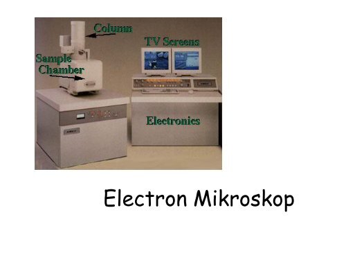
Electron Mikroskop
Electron Mikroskop
Electron Mikroskop

You also want an ePaper? Increase the reach of your titles
YUMPU automatically turns print PDFs into web optimized ePapers that Google loves.
<strong>Electron</strong> <strong>Mikroskop</strong>
Scanning <strong>Electron</strong> Microscopy (SEM)<br />
•Apa itu SEM?<br />
•Prinsip Kerja SEM<br />
•Komponen utama dan fungsinya<br />
•<strong>Electron</strong> beam - spesimen interaksi<br />
•Inteaksi volume dan escape volume<br />
•Perbesaran, resolusi, depth of field dan<br />
kontras bayangan<br />
•Energy Dispersive X-ray Spectroscopy (EDS)<br />
•Wavelength Dispersive X-ray Spectroscopy<br />
(WDS)<br />
•Orientation Imaging Microscopy (OIM)<br />
•X-ray Fluorescence (XRF)
Comparison of OM,TEM and SEM<br />
Light source<br />
Condenser<br />
Specimen<br />
Objective<br />
Eyepiece Projector<br />
Source of<br />
electrons<br />
Magnetic<br />
lenses<br />
Specimen<br />
OM TEM SEM<br />
detector<br />
CRT<br />
Cathode<br />
Ray Tube<br />
Principal features of an optical microscope, a transmission<br />
electron microscope and a scanning electron microscope,<br />
drawn to emphasize the similarities of overall design.
Glass Magnetic<br />
coils<br />
Anode<br />
Under vacuum
PERBEDAAN MO DAN SEM<br />
MO : resolusi/daya pisah<br />
lebih rendah<br />
SEM: resolusi/daya<br />
pisah lebih tinggi<br />
Kombinasi perbesaran dan daya pisah yang lebih besar dan kemampuan deteksi unsur pada<br />
permukaan material SEM lebih teliti untuk riset dan industri
I. Basics of <strong>Electron</strong> Microscopy<br />
• Electro-magnetic lenses<br />
• Scanning Transmission EM (STEM)<br />
– Mass determination<br />
– Elemental mapping<br />
• Scanning EM (SEM)<br />
– Surface relief<br />
• Transmission EM (TEM)<br />
– Structures<br />
– Imaging or Diffraction<br />
– 0.03 Å theoretical resolution<br />
1.0 Å practical resolution
II. <strong>Electron</strong> Source<br />
• Tungsten filament (thermionic)<br />
• Tungsten crystal (field emission) 100x brighter<br />
• <strong>Electron</strong>s Accelerated to defined energy<br />
behave as a wave.<br />
• kV (100 – 1000 kV with 200kV-> 0.025 Å)
<strong>Electron</strong> beam Source<br />
W or LaB6 Filament<br />
Thermionic or Field Emission Gun
ELEKTRON YANG BERHAMBUR DAN<br />
DITANGKAP SEM SAAT SAMPEL<br />
DITEMBAK ELEKTRON
HAMBURAN ELEKTRON DIDETEKSI DAN<br />
ENERGINYA DITAMPILKAN DALAM BENTUK<br />
GAMBAR DAN GRAFIK<br />
Tiap Jenis hamburan elektron<br />
ditangkap detektor yang<br />
berbeda<br />
Tempat Sampel
TEMPAT SAMPEL DI SCANNING<br />
ELECTRON MICROSCOPE
PENGAMATAN DENGAN SCANNING<br />
ELECTRON MICROSCOPE<br />
Perbesaran<br />
OM 4x – 1000x<br />
SEM 10x – 3000000x<br />
Aplikasi :<br />
•Mengamati struktur maupun<br />
bentuk permukaan yang<br />
berskala lebih halus<br />
•Dilengkapi Dengan EDS<br />
(<strong>Electron</strong> Dispersive X ray<br />
Spectroscopy)<br />
•Dapat mendeteksi unsur2<br />
dalam material.<br />
•Permukaan yang diamati<br />
harus penghantar elektron
Keuntungan SEM terhadap OM<br />
Perbesaran Depth of Field Resolusi<br />
OM 4x – 1000x 15.5mm – 0.19mm ~ 0.2mm<br />
SEM 10x – 3000000x 4mm – 0.4mm 1-10nm<br />
SEM mempunyai depth of field yang besar, yang dapat<br />
memfokus jumlah sampel yang lebih banyak pada satu<br />
waktu dan menghasilkan bayangan yang baik dari<br />
sampel tiga dimensi. SEM juga menghasilkan bayangan<br />
dengan resolusi tinggi, yang berarti mendekati bayangan<br />
yang dapat diuji dengan perbesaran tinggi.<br />
Kombinasi perbesaran yang lebih tinggi, dark field,<br />
resolusi yang lebih besar, dan komposisi serta informasi<br />
kristallografi membuat SEM merupakan satu dari<br />
peralatan yang paling banyak digunakan dalam<br />
penelitian, R&D industri khususnya industri<br />
semikonductor.
• Topography<br />
Aplikasi Utama SEM<br />
The surface features of an object and its texture<br />
(hardness, reflectivity… etc.)<br />
• Morphology<br />
The shape and size of the particles making up the<br />
object (strength, defects in IC and chips...etc.)<br />
• Composition<br />
The elements and compounds that the object is<br />
composed of and the relative amounts of them<br />
(melting point, reactivity, hardness...etc.)<br />
• Crystallographic Information<br />
How the grains are arranged in the object<br />
(conductivity, electrical properties, strength...etc.)
<strong>Electron</strong> Gun<br />
A More<br />
Detaile<br />
d Look<br />
Inside<br />
Source: L. Reimer,<br />
“Scanning <strong>Electron</strong><br />
Microscope”, 2 nd Ed.,<br />
Springer-Verlag, 1998, p.2<br />
e - beam
Preparasi Sampel<br />
• Hindari semua air, larutan atau<br />
material-material lain yang mudah<br />
menguap dalam vakum.<br />
• Permukaan harus rata untuk BSE dan<br />
OIM<br />
• Tentukan jumlah sample.<br />
• Samples Non-logam, seperti building<br />
materials, insulating ceramics, harus di<br />
caoting agar konduktivitas listriknya<br />
baik. Logam dan samples konduktivitas<br />
dapat diletakan langsung kedalam SEM.
Image Magnification<br />
Example of a series of increasing magnification (spherical lead<br />
particles imaged in SE mode)
Bagaimana Elektron Beam<br />
dihasilkan ?<br />
• Elektron guns digunakan untuk<br />
menghasilkan kontrol beam yang halus<br />
dari elektron yang kemudian difokuskan<br />
pada permukaan spesimen.<br />
• Eelektron guns bisa dalam bentuk<br />
thermionik gun atau field-emission gun
Thermionic Emission Gun<br />
• A tungsten filament<br />
heated by DC to<br />
approximately 2700K or<br />
LaB 6 rod heated to around<br />
2000K<br />
• A vacuum of 10 -3 Pa (10 -4<br />
Pa for LaB 6) is needed to<br />
prevent oxidation of the<br />
filament<br />
• <strong>Electron</strong>s “boil off” from<br />
the tip of the filament<br />
• <strong>Electron</strong>s are accelerated<br />
by an acceleration voltage<br />
of 1-50kV
Field Emission Gun<br />
• The tip of a tungsten needle is<br />
made very sharp (radius < 0.1<br />
mm)<br />
• The electric field at the tip is<br />
very strong (> 10 7 V/cm) due<br />
to the sharp point effect<br />
• <strong>Electron</strong>s are pulled out from<br />
the tip by the strong electric<br />
field<br />
• Ultra-high vacuum (better than<br />
10 -6 Pa) is needed to avoid ion<br />
bombardment to the tip from<br />
the residual gas.<br />
• <strong>Electron</strong> probe diameter < 1<br />
nm is possible
Filament<br />
Source of <strong>Electron</strong>s<br />
T: ~1500o Thermionic Gun<br />
C<br />
W and LaB 6<br />
(5-50mm)<br />
E: >10MV/cm<br />
(5nm)<br />
Cold- and thermal FEG<br />
<strong>Electron</strong> Gun Properties<br />
Source Brightness Stability(%) Size Energy spread Vacuum<br />
W 3X10 5 ~1 50mm 3.0(eV) 10 -5 (t )<br />
LaB 6 3x10 6 ~2 5mm 1.5 10 -6<br />
C-FEG 10 9 ~5 5nm 0.3 10 -10<br />
T-FEG 10 9
Lensa Magnetik<br />
• Lensa Condenser – focusing<br />
determines the beam current<br />
which impinges on the sample.<br />
• Lensa Objective – final probe<br />
forming<br />
determines the final spot size of<br />
the electron beam, i.e., the<br />
resolution of a SEM.
Kenapa perlu Vakum?<br />
Bila SEM digunakan, kolum elektron-optik<br />
dan sampel chamber harus selalu pada<br />
kondisi vakum.<br />
1. Bila kolum ada gas didalamnya maka elektron akan<br />
diskaterd oleh molekul gas yang menyebabkan<br />
intensitas dan stability beam akan berkurang<br />
2. Molekul-molekul gas lain, yang datang dari sampel<br />
atau dari microskop itu sendiri, dapat membentuk<br />
persenyawaan dan kondens pada sampel. Ini akan<br />
membuatan kontras menjadi lebih rendah dan<br />
bayangan menjadi kabur.
<strong>Electron</strong> Detectors and Sample Stage<br />
Objective<br />
lens<br />
Sample stage
Coating Techniques<br />
Sputter coater is used to coat insulating samples<br />
Au and Al – good for SE yield<br />
AuPd alloy – good for high resolution<br />
C – used if X-ray microanalysis is required<br />
Coating should have low granularity in order not to<br />
mask the underlying structure (
OIM-Grain Boundary Maps<br />
Grain Boundary Map Orientation Map<br />
A Grain boundary Map can be generated by comparing the orientation<br />
between each pair of neighboring points in an OIM scan. A line is<br />
drawn separating a pair of points if the difference in orientation<br />
between the points exceeds a given tolerance angle. An Orientation<br />
Map is generated by shading each point in the OIM scan according to<br />
some parameter reflecting the orientation at each point. Both of these<br />
maps are shown overlaid on the digital micrograph from the SEM.