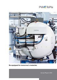
Be equipped for tomorrow's materials - PVA TePla AG
Be equipped for tomorrow's materials - PVA TePla AG
Be equipped for tomorrow's materials - PVA TePla AG

You also want an ePaper? Increase the reach of your titles
YUMPU automatically turns print PDFs into web optimized ePapers that Google loves.
<strong>PVA</strong> <strong>TePla</strong><br />
<strong>Be</strong> <strong>equipped</strong> <strong>for</strong> tomorrow‘s <strong>materials</strong><br />
Overview<br />
SiCube
The <strong>PVA</strong> <strong>TePla</strong> Group<br />
The companies of the <strong>PVA</strong> <strong>TePla</strong> Group develop and manufacture systems and components<br />
serving a broad range of markets globally <strong>for</strong> the treatment and finishing of high value<br />
<strong>materials</strong> and surfaces. The necessary processes take place mainly under:<br />
Vacuum High temperatures Pressure<br />
Plasma<br />
<strong>PVA</strong> <strong>TePla</strong> <strong>AG</strong> together with its subsidiaries is a key player in the world <strong>for</strong> hard metal<br />
sintering systems, crystal-growing systems and plasma systems used <strong>for</strong> surface activation<br />
and ultra-fine cleaning. The equipment and services of <strong>PVA</strong> <strong>TePla</strong> enable important<br />
manufacturing processes and technological developments, primarily in the promising<br />
semiconductor, hard metal, electrical/electronic and optical industries – as well as in the<br />
areas of energy, communication, photovoltaic and environmental technology.<br />
2
3<br />
The Divisions<br />
Industrial<br />
Systems<br />
<strong>PVA</strong> <strong>TePla</strong> <strong>AG</strong><br />
Semiconductor<br />
Systems<br />
Solar<br />
Systems<br />
Equipment <strong>for</strong> treating and refining <strong>materials</strong> are manufactured in the Industrial Systems<br />
division. In vacuum, under controlled inert or in a reactive gas atmosphere with partial<br />
and high pressure or in plasma, the properties of the <strong>materials</strong> can be improved, their<br />
shape can be changed and parts of different <strong>materials</strong> can be brazed or diffusion bonded<br />
to each other.<br />
In the Semiconductor Systems division, <strong>PVA</strong> <strong>TePla</strong> offers a range of innovative high-tech<br />
equipment: systems <strong>for</strong> the production of silicon crystals <strong>for</strong> the semiconductor and<br />
optoelectronic industry, systems <strong>for</strong> plasma treatment of semiconductor devices and<br />
components and solutions <strong>for</strong> nondestructive quality inspection <strong>for</strong> <strong>materials</strong> and components<br />
using ultrasound, infrared lasers and chemical etching.<br />
In the Solar Systems division advanced crystallization and auxiliary equipment is provided<br />
<strong>for</strong> manufacturing of both mono and multi crystalline ingots. Competitive costs of ownerhsip,<br />
product customization and extended service and support are the key to the success<br />
of leading customers and partners in Photovoltaics.
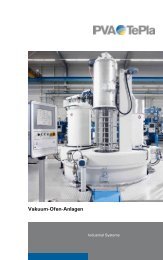
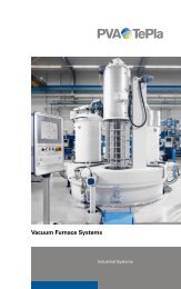
Industrial Systems<br />
Vacuum Systems<br />
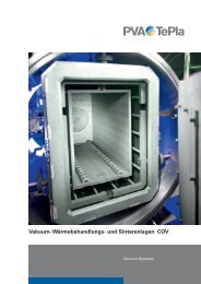
In the Vacuum Systems business unit, <strong>PVA</strong> <strong>TePla</strong> <strong>AG</strong> specializes in the design and<br />
construction of thermal systems developing, manufacturing and treating high-quality <strong>materials</strong><br />
at high temperatures. With more than 50 years’ experience and an equipment<br />
install base of over 1,000 systems, the company is a global market leader especially <strong>for</strong><br />
vacuum and pressure sintering systems.<br />
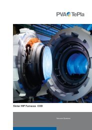
Sintering – in Vacuum and Pressure<br />
The vacuum sintering systems and the pressure sintering systems are designed <strong>for</strong> all applications<br />
relating to debinding and vacuum sintering, and the pressure sintering systems<br />
are designed <strong>for</strong> subsequent isostatic pressing of powders from metals, carbides, alloys<br />
and ceramics under vacuum, inert or active gas atmosphere and high gas pressure of up<br />
to 100 bar.<br />
High Temperature Graphite Heat Treatment<br />
High value engineered components made of graphite or graphite-compounds (CFC) are<br />
purified, graphitized, infiltrated or coated under high temperatures in excess of 2,000 °C<br />
and vacuum or reactive gases <strong>for</strong> its use in semiconductor or photovoltaic production systems,<br />
automotive, aerospace applications and optoelectronics.<br />
Brazing and Diffusion Bonding<br />
Use of these advanced joining methods is often an essential part of the manufacture of<br />
complex components, including those made from highly contrasting <strong>materials</strong>. These<br />
processes enable the utmost precision, purity and accuracy of the connections.<br />
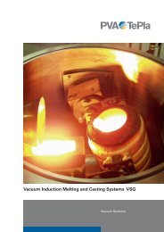
Melting and Casting<br />
The vacuum melting and casting systems can be used <strong>for</strong> all applications in inductive<br />
melting of metals and special alloys under high vacuum and inert gas, e.g. in <strong>materials</strong><br />
development (R&D), purification and moulded cast of precious metals or precision casting<br />
of e.g. turbine parts.<br />
4
5<br />
Heat Treatment and Special Systems<br />
Our vacuum systems are individually designed <strong>for</strong> a wide variety of processes in accordance<br />
with customer requirements. In addition, to the above-mentioned processes, these<br />
include reduction, carburizing, cleaning, tempering, degassing, coating, granulation,<br />
distillation, impregnation and drying.<br />
Systems <strong>for</strong> PulsPlasma ® Nitriding and Plasma Activation<br />
Our subsidiary PlaTeG GmbH develops and produces plasma systems <strong>for</strong> a wide range<br />
of industrial applications.<br />
Systems <strong>for</strong> PulsPlasma ® Nitriding<br />
PulsPlasma ® nitriding is a thermo-chemical heat treatment <strong>for</strong> the creation of hardened and<br />
wear resistant Iron-nitride layers on steel surfaces. It is used <strong>for</strong> surface treatment of steel<br />
workpieces <strong>for</strong> wear protection. We develop and manufacture PulsPlasma ® nitriding units in<br />
all sizes from small laboratory units to standard units <strong>for</strong> hardening shops up to large custom<br />
units <strong>for</strong> the treatment of large tools and gears with chamber diameters > 4.3 m.<br />
Plasma Activation/Plasma Polymerization Systems<br />
Plasma activation is used to increase the surface energy of glass, ceramics and<br />
plastics <strong>for</strong> better bonding, painting or printing properties. In plasma polymerization,<br />
hydrophilic or hydrophobic layers are produced to reduce friction or to protect against<br />
corrosion.<br />
Plasma Sterilization Systems<br />
With plasma sterilization, medical durables and consumables are sterilized in a gentle,<br />
environmentally sound and energy-efficient manner.
Semiconductor Systems<br />
Crystal Growing Systems<br />
<strong>PVA</strong> <strong>TePla</strong> is a key equipment supplier <strong>for</strong> the semiconductor industry. The company offers<br />
all industrially relevant methods <strong>for</strong> crystal growth, particularly <strong>for</strong> monocrystalline silicon<br />
crystals.<br />
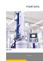
Crucible-Pulling-from-the-melt-Method (Czochralski-Cz) – EKZ Type<br />
We offer Cz-systems <strong>for</strong> pulling silicon and germanium crystals <strong>for</strong> wafer manufacture <strong>for</strong><br />
the semiconductor industry. Equipment <strong>for</strong> the growth of crystal diameters of up to 450<br />
mm are available.<br />
Vertical Gradient Freeze (VGF) Method – Kronos Type<br />
For compound semiconductors in the optoelectronic industry and <strong>for</strong> high-frequency<br />
applications, we offer high-pressure VGF systems <strong>for</strong> crystal manufacture (gallium arsenide<br />
[GaAs] and indium phosphide [InP]).<br />
Floatzone (FZ) Method – FZ Type<br />
With systems using this method, high-purity monocrystalline <strong>materials</strong> are produced<br />
according to the “FZ-method”. These crystals are used in the high-per<strong>for</strong>mance<br />
electronics sector and polysilicon production. Several variations of the equipment are<br />
available <strong>for</strong> a wide range of applications.<br />
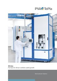
Silicon Carbide (SiC) Crystallisation by HTCVD/HTCVT Method – SiCube Type<br />
SiC-crystals produced in the SiCube are needed in high-technology market areas. Typical<br />
applications are the high power electronics and optoelectronics, where specific properties<br />
of the SiC material, like high thermal conductivity, are crucial.<br />
6
7<br />
Plasma Systems<br />
Low-pressure plasma systems <strong>for</strong> customer-specific solutions are designed and manufactured<br />
by this business unit. With gas plasma, surfaces can be functionalized on a<br />
nano-scale level or cleaned with excellent precision. Without the use of environmentally<br />
unfriendly wet chemistries we offer our customers the entire range of atmospheric and<br />
low-pressure gas plasma technologies which utilize both microwave (Mw) and radio frequency<br />
(Rf) excitation <strong>for</strong> the following markets and applications:<br />
Semiconductor<br />
Our core competence in this area is the removal (ashing) and processing of photoresist<br />
masks <strong>for</strong> micro- and nano-structuring. We also offer similar process solutions <strong>for</strong> the<br />
MEMS sensor, high-brightness LED, OLED display and solar market. We offer a complete<br />
range of products in both batch and single-wafer configurations. In the Backend<br />
Chip Packaging, equipment <strong>for</strong> cleaning and activation as well as precise thinning of<br />
wafers (thickness
Analytical Systems<br />
By this business unit a number of measuring systems <strong>for</strong> nondestructive quality inspection<br />
with unique methods and analysis software is offered.<br />
Laserbased Wafer Metrology Systems<br />
These fully automated systems are capable of handling wafer sizes of up to 300 mm. The<br />
equipment is used <strong>for</strong> quality control in semiconductor production fabs globally in two<br />
main areas of application: <strong>for</strong> measuring critical shear stresses in silicon wafers, and <strong>for</strong><br />
measuring the uni<strong>for</strong>mity of ion implantation processes.<br />
Acoustic Scanning Microscopes<br />
Ultrasound electron scanning microscopes have a frequency ranges of 1 MHz – 2 GHz,<br />
offering the best resolutions available in the market today. The method enables nondestructive<br />
identification of defects in high-tech <strong>materials</strong> <strong>for</strong> the semiconductor and optoelectronic<br />
industry, e.g. <strong>for</strong> IC inspection and failure analysis, MEMS, bonded wafer structures,<br />
LEDs and also silicon ingots with a diameter of up to 450 mm. Newly developed<br />
methods also enable applications in medical research (imaging and analysis of cells) and<br />
the characterization of material parameters <strong>for</strong> solid state physics and material-analysis.<br />
Vapour-Phase-Decomposition Systems<br />
These innovative analytical systems are used to trace surface impurities on wafers <strong>for</strong><br />
the semiconductor industry. In particular, metallic impurities can be found also in the production<br />
process with exceptional sensitivity and reproducibility. Fully automated systems<br />
that use VPD technology in conjunction with mass spectrometric-analytical procedures<br />
(ICP-MS) satisfy the strictest requirements with respect to determining the contamination<br />
level of wafers and microelectronic components.<br />
8
9<br />
Solar Systems<br />
The Solar Systems division primarily builds crystallization equipment <strong>for</strong> silicon ingot manufacturing<br />
<strong>for</strong> solar cell application.<br />
MonoCrystallizer - Czochralski (Cz) Method <strong>for</strong> Mono Crystal Ingots<br />
Our crystallization equipment features advanced crystallization processes and offers<br />
our customers high yield and low cost <strong>materials</strong>.<br />
MultiCrystallizer - Vertical Gradient Freeze (VGF) Method <strong>for</strong> Multi Crystal Ingots<br />
The VGF-furnace features advanced process versatility <strong>for</strong> the casting of multicrystalline<br />
material. The equipment offers very high throughput and has been designed with the<br />
highest safety standards available today.<br />
Integrated Solutions <strong>for</strong> Silicon Wafers<br />
Crystallization equipment from <strong>PVA</strong> <strong>TePla</strong> can be supplied as an integrated solution featuring<br />
e.g. feeding of raw material, argon recycling, crucible loading and ingot removal<br />
systems, auxiliary equipment <strong>for</strong> thermal cracking of feedstock and recycled material etc.<br />
Together with associated industry partners we can offer all of our solar silicon equipment<br />
and software solutions as an integral part of a wafering turnkey line. <strong>PVA</strong> <strong>TePla</strong> offerings <strong>for</strong><br />
solar silicon incorporate leading edge design and technologies providing our customers<br />
both rugged and highly reliable per<strong>for</strong>mance <strong>for</strong> manufacturing in the typical installation<br />
environment of solar wafer fabs.
Contact Details<br />
Industrial Systems:<br />
Vacuum Systems:<br />
<strong>PVA</strong> <strong>TePla</strong> <strong>AG</strong> Phone +49 (641) 6 86 90 – 0<br />
Im Westpark 10 –12 Fax +49 (641) 6 86 90 – 800<br />
35435 Wettenberg E-mail info @pvatepla.com<br />
Germany Home www.pvatepla.com<br />
PulsPlasma ® Nitriding and Plasma Activation:<br />
PlaTeG GmbH Phone + 49 (641) 6 86 90 – 490<br />
Im Westpark 10 –12 Fax + 49 (641) 6 86 90 – 498<br />
35435 Wettenberg E-mail service@plateg.de<br />
Germany Home www.plateg.de<br />
Semiconductor Systems:<br />
Crystal Growing Systems:<br />
<strong>PVA</strong> <strong>TePla</strong> <strong>AG</strong> Phone +49 (641) 6 86 90 – 0<br />
Im Westpark 10 –12 Fax +49 (641) 6 86 90 – 800<br />
35435 Wettenberg E-mail info @pvatepla.com<br />
Germany Home www.pvatepla.com<br />
Plasma Systems:<br />
Semiconductor<br />
<strong>PVA</strong> <strong>TePla</strong> <strong>AG</strong><br />
Plasma Systems Phone +49 (89) 905 03 – 0<br />
Ammerthalstr. 34 Fax +49 (89) 905 03 – 185<br />
85551 Kirchheim E-mail plasma@pvatepla.com<br />
Germany Home www.tepla.com<br />
Life Science / Industry<br />
<strong>PVA</strong> <strong>TePla</strong> America Inc. Phone +1 (800) 527 5667<br />
251 Corporate Terrace, Fax +1 (951) 371 9792<br />
Corona CA 92879 E-mail sales@pvateplaamerica.com<br />
USA Home www.pvateplaamerica.com<br />
10
11<br />
Analytical Systems:<br />
Laserbased Wafer Metrology Systems<br />
<strong>PVA</strong> <strong>TePla</strong> <strong>AG</strong> Phone +49 (89) 905 03 – 0<br />
Ammerthalstr. 34 Fax +49 (89) 905 03 – 185<br />
85551 Kirchheim E-mail plasma@pvatepla.com<br />
Germany Home www.tepla.com<br />
Acoustic Scanning Microscopes<br />
<strong>PVA</strong> <strong>TePla</strong> Analytical<br />
Systems GmbH Phone +49 (7363) 95 44 – 0<br />
Deutschordenstrasse 38 Fax +49 (7363) 95 44 – 113<br />
73463 Westhausen E-mail saminfo@pvatepla.com<br />
Germany Home www.pva-analyticalsystems.com<br />
Vapour Phase Decomposition Systems<br />
Munich<br />
Metrology GmbH Phone +49 (89) 189 65 89 – 0<br />
Garmischer Strasse 35 Fax +49 (89) 189 65 89 – 09<br />
81373 München E-mail info@munich-metrology.com<br />
Germany Home www.munich-metrology.com<br />
Solar Systems:<br />
<strong>PVA</strong> <strong>TePla</strong> <strong>AG</strong> Phone +49 (641) 6 86 90 – 0<br />
Im Westpark 10 –12 Fax +49 (641) 6 86 90 – 800<br />
35435 Wettenberg E-mail info @pvatepla.com<br />
Germany Home www.pvatepla.com
<strong>PVA</strong> <strong>TePla</strong> <strong>AG</strong><br />
Im Westpark 10 –12<br />
35435 Wettenberg<br />
Germany<br />
Rev. - Stand: 011<br />
Phone +49 (641) 6 86 90 - 0<br />
Fax +49 (641) 6 86 90 - 800<br />
E-Mail info @pvatepla.com<br />
Home www.pvatepla.com