Be equipped for tomorrow's materials - PVA TePla AG
Be equipped for tomorrow's materials - PVA TePla AG
Be equipped for tomorrow's materials - PVA TePla AG

Create successful ePaper yourself
Turn your PDF publications into a flip-book with our unique Google optimized e-Paper software.
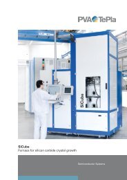
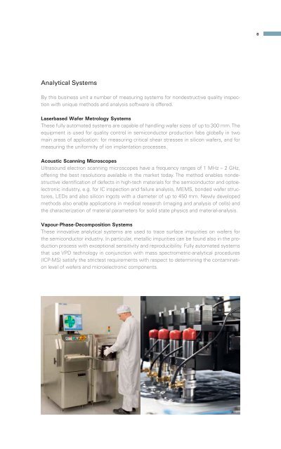
Analytical Systems<br />
By this business unit a number of measuring systems <strong>for</strong> nondestructive quality inspection<br />
with unique methods and analysis software is offered.<br />
Laserbased Wafer Metrology Systems<br />
These fully automated systems are capable of handling wafer sizes of up to 300 mm. The<br />
equipment is used <strong>for</strong> quality control in semiconductor production fabs globally in two<br />
main areas of application: <strong>for</strong> measuring critical shear stresses in silicon wafers, and <strong>for</strong><br />
measuring the uni<strong>for</strong>mity of ion implantation processes.<br />
Acoustic Scanning Microscopes<br />
Ultrasound electron scanning microscopes have a frequency ranges of 1 MHz – 2 GHz,<br />
offering the best resolutions available in the market today. The method enables nondestructive<br />
identification of defects in high-tech <strong>materials</strong> <strong>for</strong> the semiconductor and optoelectronic<br />
industry, e.g. <strong>for</strong> IC inspection and failure analysis, MEMS, bonded wafer structures,<br />
LEDs and also silicon ingots with a diameter of up to 450 mm. Newly developed<br />
methods also enable applications in medical research (imaging and analysis of cells) and<br />
the characterization of material parameters <strong>for</strong> solid state physics and material-analysis.<br />
Vapour-Phase-Decomposition Systems<br />
These innovative analytical systems are used to trace surface impurities on wafers <strong>for</strong><br />
the semiconductor industry. In particular, metallic impurities can be found also in the production<br />
process with exceptional sensitivity and reproducibility. Fully automated systems<br />
that use VPD technology in conjunction with mass spectrometric-analytical procedures<br />
(ICP-MS) satisfy the strictest requirements with respect to determining the contamination<br />
level of wafers and microelectronic components.<br />
8