Maximizing DAC Performance for Every Budget - ESS Technology, Inc.
Maximizing DAC Performance for Every Budget - ESS Technology, Inc.
Maximizing DAC Performance for Every Budget - ESS Technology, Inc.

Create successful ePaper yourself
Turn your PDF publications into a flip-book with our unique Google optimized e-Paper software.
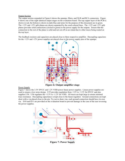
Output Section<br />
The output section expanded in Figure 6 shows the opamps, filters, and XLR and RCA connectors. Figure<br />
6 shows one of the eight identical output stages on the evaluation board. The top copper layer of the PCB is<br />
shown in red, the bottom is shown in dark blue and notes <strong>for</strong> the purpose of this document are in green.<br />
The +12V and -12V split planes are shown separated by the coral colored lines. The +12V and -12V split<br />
planes provides solid connections (circled in green) to the power supply <strong>for</strong> the outputs. Ensure that the<br />
connection to the rest of the plane is solid and not cut off on an island due to other traces being routed on<br />
the top layer.<br />
The feedback resistors and capacitors are placed close to there respective amplifier. Decoupling capacitors<br />
<strong>for</strong> the +12V and -12V power supplies are placed close to the power supply pins of the opamps.<br />
Figure 6: Output amplifier stage<br />
Power Supply<br />
Figure 7 shows the 3.3V DVCC and 1.2V VDD power linear power supplies. Linear power supplies are<br />
used to ensure a low noise design. U55 provides regulation from +12V to +3.3V <strong>for</strong> DVCC and also<br />
supplies U56. U56 regulates the +3.3V to +1.2V <strong>for</strong> VDD. All traces are kept large to ensure minimal<br />
trace resistance. Decoupling capacitance is kept close to the linear regulator. Ground connections are kept<br />
short with a via placed close to the pin. Try not to share vias, each ground connection should have its own<br />
via. D10 and D11 are provided on the evaluation board to prevent damage in the case of the user reversing<br />
the power supplies.<br />
Figure 7: Power Supply