Maximizing DAC Performance for Every Budget - ESS Technology, Inc.
Maximizing DAC Performance for Every Budget - ESS Technology, Inc.
Maximizing DAC Performance for Every Budget - ESS Technology, Inc.

Create successful ePaper yourself
Turn your PDF publications into a flip-book with our unique Google optimized e-Paper software.
Application Note<br />
<strong>Maximizing</strong> <strong>DAC</strong> <strong>Per<strong>for</strong>mance</strong> <strong>for</strong> <strong>Every</strong> <strong>Budget</strong><br />
Abstract<br />
This application note discusses several factors that affect the audio per<strong>for</strong>mance of the Sabre digital audio<br />
converters. This article shows examples of possible tradeoffs <strong>for</strong> bill of materials cost vs. per<strong>for</strong>mance.<br />
The differences between topologies, PCB layouts, and components used are discussed with emphasis on<br />
BOM cost vs. per<strong>for</strong>mance.<br />
Introduction<br />
Design engineers face the challenge extracting the best possible per<strong>for</strong>mance from the least expensive<br />
circuit possible. The combination of digital logic with very low noise analog signals in a confined space<br />
presents a significant challenge to the PCB layout engineer. Designing a circuit that has a BOM under<br />
budget and meets per<strong>for</strong>mance requirements presents a compromise to the design engineer. This may be<br />
the ultimate per<strong>for</strong>mance, cost is no object, best in the world audiophile design, or a lowest cost, high<br />
per<strong>for</strong>mance solution, that out per<strong>for</strong>ms the competition.<br />
Choosing the <strong>DAC</strong><br />
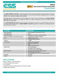
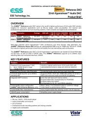
The ES9008 Reference <strong>DAC</strong> and the lower cost Premier ES9006 <strong>DAC</strong> are currently the available options<br />
when choosing an <strong>ESS</strong> <strong>Technology</strong> <strong>Inc</strong>. Sabre <strong>DAC</strong>. The Sabre Product Brief on <strong>ESS</strong> <strong>Technology</strong> <strong>Inc</strong>.<br />
website provides an overview of the features and per<strong>for</strong>mance expectations of both choices.<br />
Choosing an output stage topology<br />
<strong>ESS</strong> <strong>Technology</strong> has designed a few different output stages <strong>for</strong> use with the Sabre <strong>DAC</strong>’s. If desired, the<br />
<strong>DAC</strong> output channels can be combined to increase the signal to noise per<strong>for</strong>mance of the <strong>DAC</strong>. The output<br />
impedance of the <strong>DAC</strong> is decreased by the number of paralleled outputs; there<strong>for</strong>e the output stage gain<br />
must also be decreased accordingly.<br />
The typical per<strong>for</strong>mance numbers as measured on the Sabre evaluation boards are provided in Table 1.
Differential Output Single Ended Output<br />
Op Amp Part Number<br />
THD (dB) DNR (dB) THD (dB) DNR (dB)<br />
<strong>ESS</strong> Reference Evaluation Board ES9008 2CH +/-12V Figure 1 and Figure 2, 4 <strong>DAC</strong> channels in<br />
parallel, R1 and R4 = 680 ohms<br />
AD797<br />
-116 -132 -116 -128<br />
LME49710<br />
-114 -126 -114 -124<br />
<strong>ESS</strong> Reference Evaluation Board ES9008 8CH +/-12V Figure 1 and Figure 2<br />
AD797<br />
-114 -128 -114 -126<br />
LME49710<br />
-114 -126 -114 -124<br />
NE5534<br />
-112 -125 -110 -124<br />
NE5534 <strong>for</strong> audio and AD797 <strong>for</strong> AVCC<br />
Regulator<br />
-111 -126 -110 -124<br />
OPA2134 <strong>for</strong> audio and AD797 <strong>for</strong> AVCC<br />
Regulator<br />
-112 -120 -111 -120<br />
<strong>ESS</strong> Evaluation Board ES9008 8CH LC SS +12V Figure 3<br />
LME49720<br />
N/A N/A -112 -118<br />
<strong>ESS</strong> Evaluation Board ES9006 8CH +/-12V Figure 1 and Figure 2<br />
AD797<br />
-104 -124 -104 -123<br />
NE5534<br />
-104 -118 -104 -117<br />
<strong>ESS</strong> Evaluation Board ES9006 8CH LC SS +12V Figure 3<br />
LME49720<br />
ROHM 4560<br />
N/A N/A -106 -118<br />
N/A N/A -105 -114<br />
Table 1 EVB <strong>Per<strong>for</strong>mance</strong><br />
The highest per<strong>for</strong>mance circuit is provided on the Sabre Reference Evaluation Board. This circuit is<br />
shown in Figure 1.<br />
Figure 1: Sabre Reference Evaluation Board Differential Output
The Sabre Reference Evaluation Board also provides single ended outputs, this circuit is shown in Figure 2.<br />
Figure 2: Sabre Reference Evaluation Board Single Ended Output<br />
Note: The first half of the circuits in Figures 1 and 2 are identical, Point A and Point B are the same points<br />
in both the circuits.<br />
For the lowest cost solution the circuit in Figure 3 provides excellent per<strong>for</strong>mance in both THD and SNR<br />
with the fewest possible components.<br />
Figure 3: Sabre Premier Evaluation Board Single Ended Output
Component Selection<br />
In order to extract the highest per<strong>for</strong>mance from the <strong>DAC</strong>, the following components in all the above<br />
topologies are critical:<br />
Capacitors<br />
All surface mount chip capacitors that are in the audio path must be COG dielectric. Dielectrics such as<br />
X7R and X5R cause nonlinearities this causes the total harmonic distortion to drastically degrade.<br />
Resistors<br />
For optimum THD and SNR the surface mount resistors within the audio path must be thin film resistors.<br />
Thick film surface mount resistors should be avoided as they have a Voltage Coefficient of Resistance<br />
approximately 100 times higher than thin film resistors. Metal film resistors also have a very low VCR but<br />
are typically higher cost.<br />
Operation Amplifiers<br />
Operational amplifiers typically are the most expensive component in the circuit. The choice of opamp<br />
varies <strong>for</strong> each design and budget. The power supply circuit shown in Figure 4 is necessary to provide a<br />
clean 3.3V to the analog section of the Sabre <strong>DAC</strong>. The opamp used <strong>for</strong> this circuit is the most critical <strong>for</strong><br />
optimizing the THD and SNR per<strong>for</strong>mance. Use of a poorly designed opamp will degrade both the THD<br />
and SNR. This opamp may oscillate at a high frequency when driving the highly capacitive load of the<br />
AVCC decoupling capacitors. C2 can be reduced from 47uF to 10uF if a high per<strong>for</strong>mance opamp is used.<br />
The Rohm 4560 tends to oscillate at high frequency when driving a moderately capacitive load, but stop<br />
oscillating when that capacitive load is larger than ~30uF. C1 may be reduced to 1uF without observable<br />
consequences when using either the AD797 or LME opamps listed below.<br />
Figure 4: AVCC +3.3V Filter and Regulator<br />
<strong>ESS</strong> recommends the opamps listed below. They are sorted from highest to lowest per<strong>for</strong>mance.<br />
Manufacturer Part Number<br />
Analog Devices AD797<br />
National Semiconductor LME49710, LME49720, LME49740, LM4562<br />
Texas Instruments NE5534, NE5532<br />
Rohm 4560
Master Clock<br />
As detailed in the datasheet, the MCLK must be at least 386*Fs <strong>for</strong> SPDIF inputs and 192*Fs <strong>for</strong><br />
Serial/DSD inputs. For optimum jitter tolerance the MCLK should be at least 10% higher than this<br />
theoretical MCLK minimum, this ensures audio clarity free from input clock jitter.<br />
If operating with a synchronous MCLK, it is recommended to use an inverted MCLK. The inverted<br />
synchronous MCLK ensures that the Sabre noise is as low as possible.<br />
Printed Circuit Board Design<br />
Proper PCB layout <strong>for</strong> the Sabre <strong>DAC</strong> is vital to the circuit’s per<strong>for</strong>mance. Time spent achieving optimum<br />
component placement provides a good foundation to make the routing task provide the best per<strong>for</strong>ming<br />
circuit within the real estate provided. <strong>Every</strong> design will have different requirements, PCB stackup, via<br />
size, PCB size, component sizes, etc. <strong>ESS</strong> has experimented with <strong>DAC</strong> evaluation PCBs ground planes to<br />
determine any benefit of split plane grounds <strong>for</strong> analog and digital ground. It is our finding and<br />
recommendation to use only one ground plane <strong>for</strong> both digital and analog grounds as it simplifies layout<br />
and provides no per<strong>for</strong>mance degradation. The most important <strong>for</strong> <strong>DAC</strong> per<strong>for</strong>mance is the ground plane,<br />
it should be as solid as possible with as few traces routed through the ground plane as possible. Any traces<br />
that are routed through the ground plane and block the “line of sight” from the <strong>DAC</strong> output to the opamp<br />
output stage significantly degrades the output THD. <strong>ESS</strong> recommends using the evaluation board designs<br />
as a guide <strong>for</strong> your own PCB layout. Critical PCB layout items:<br />
1.) Make the ground plane as solid as possible. Try to keep all ground connections as short as possible.<br />
<strong>Every</strong> ground connection should have its own via, do not share vias if possible.<br />
2.) Keep opamp feedback paths as close as possible to the opamp.<br />
3.) Ensure every opamp and <strong>DAC</strong> has decoupling capacitance on its power supply right next to the power<br />
supply pins.<br />
4.) The audio path between the <strong>DAC</strong> and the opamp stage should be kept as short and clean as possible.<br />
5.) The audio path after the opamps is not as critical.<br />
6.) Try to keep the digital circuitry away from the analog circuitry.<br />
Figure 5 shows the Sabre <strong>DAC</strong> Reference 64LQFP Evaluation Board. Each section of the circuit board is<br />
described in detail below.<br />
Figure 5: Sabre <strong>DAC</strong> Reference 64LQFP Evaluation Board
Output Section<br />
The output section expanded in Figure 6 shows the opamps, filters, and XLR and RCA connectors. Figure<br />
6 shows one of the eight identical output stages on the evaluation board. The top copper layer of the PCB is<br />
shown in red, the bottom is shown in dark blue and notes <strong>for</strong> the purpose of this document are in green.<br />
The +12V and -12V split planes are shown separated by the coral colored lines. The +12V and -12V split<br />
planes provides solid connections (circled in green) to the power supply <strong>for</strong> the outputs. Ensure that the<br />
connection to the rest of the plane is solid and not cut off on an island due to other traces being routed on<br />
the top layer.<br />
The feedback resistors and capacitors are placed close to there respective amplifier. Decoupling capacitors<br />
<strong>for</strong> the +12V and -12V power supplies are placed close to the power supply pins of the opamps.<br />
Figure 6: Output amplifier stage<br />
Power Supply<br />
Figure 7 shows the 3.3V DVCC and 1.2V VDD power linear power supplies. Linear power supplies are<br />
used to ensure a low noise design. U55 provides regulation from +12V to +3.3V <strong>for</strong> DVCC and also<br />
supplies U56. U56 regulates the +3.3V to +1.2V <strong>for</strong> VDD. All traces are kept large to ensure minimal<br />
trace resistance. Decoupling capacitance is kept close to the linear regulator. Ground connections are kept<br />
short with a via placed close to the pin. Try not to share vias, each ground connection should have its own<br />
via. D10 and D11 are provided on the evaluation board to prevent damage in the case of the user reversing<br />
the power supplies.<br />
Figure 7: Power Supply
AVCC Regulator<br />
The +3.3V required <strong>for</strong> the analog section of the <strong>DAC</strong> needs to be as quiet and well regulated as possible.<br />
The design uses the +3.3V DVCC as a reference and filters this signal with a RC filter. The opamp is<br />
configured in a buffer stage to supply the +3.3V <strong>for</strong> AVCC. As shown in Figure 8, the decoupling<br />
capacitors should be kept close to the supply pins and the filter should be close to the opamp input. The<br />
output trace with should be large and provide a very low impedance path to the <strong>DAC</strong> AVCC pins.<br />
Figure 8: AVCC Regulator
<strong>DAC</strong> and MCLK<br />
Figure 9 shows the <strong>DAC</strong> and MCLK section of the evaluation board. The ground plane should be<br />
unobstructed from the <strong>DAC</strong> outputs to the output amplifier stage. The crystal oscillator should be kept<br />
close to the <strong>DAC</strong>. Digital lines are routed away from the audio lines at the bottom of the figure. All power<br />
supply connections have decoupling capacitors place close to <strong>DAC</strong> pins.<br />
Figure 9: <strong>DAC</strong> and Oscillator<br />
SPDIF<br />
The SPDIF interface uses a comparator to clean up the input signal. The SPDIF input signal sees a 75 ohm<br />
impedance to ground.<br />
Note: Some early evaluation board designs had the 75 ohm resistor in series with the input and thus did not<br />
provide a proper 75 ohm termination impedance.<br />
Microcontroller<br />
To minimize the risk of digital noise affecting the per<strong>for</strong>mance of the <strong>DAC</strong>, a separate +3.3V supply<br />
powers the microcontroller. Decoupling capacitors are kept close to the power pins. The USB ground is<br />
isolated from the common ground plane.