Combining High-Resolution Pulsed TIVA and ... - ASM International
Combining High-Resolution Pulsed TIVA and ... - ASM International
Combining High-Resolution Pulsed TIVA and ... - ASM International

Create successful ePaper yourself
Turn your PDF publications into a flip-book with our unique Google optimized e-Paper software.
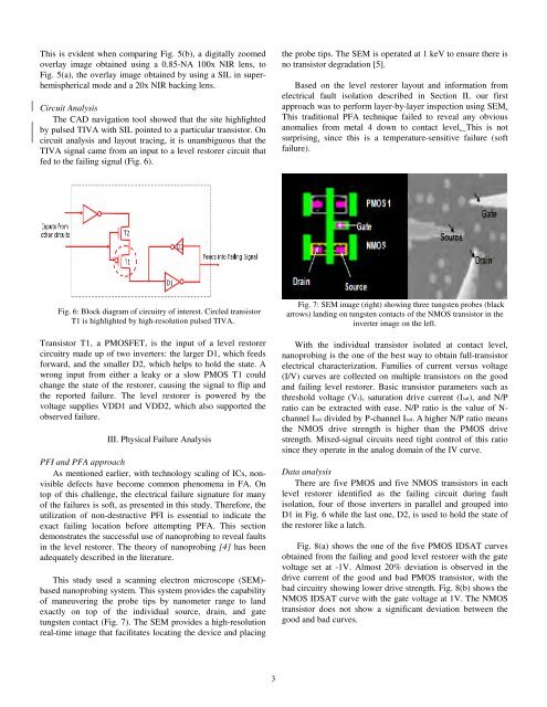
This is evident when comparing Fig. 5(b), a digitally zoomed<br />
overlay image obtained using a 0.85-NA 100x NIR lens, to<br />
Fig. 5(a), the overlay image obtained by using a SIL in superhemispherical<br />
mode <strong>and</strong> a 20x NIR backing lens.<br />
Circuit Analysis<br />
The CAD navigation tool showed that the site highlighted<br />
by pulsed <strong>TIVA</strong> with SIL pointed to a particular transistor. On<br />
circuit analysis <strong>and</strong> layout tracing, it is unambiguous that the<br />
<strong>TIVA</strong> signal came from an input to a level restorer circuit that<br />
fed to the failing signal (Fig. 6).<br />
Fig. 6: Block diagram of circuitry of interest. Circled transistor<br />
T1 is highlighted by high-resolution pulsed <strong>TIVA</strong>.<br />
Transistor T1, a PMOSFET, is the input of a level restorer<br />
circuitry made up of two inverters: the larger D1, which feeds<br />
forward, <strong>and</strong> the smaller D2, which helps to hold the state. A<br />
wrong input from either a leaky or a slow PMOS T1 could<br />
change the state of the restorer, causing the signal to flip <strong>and</strong><br />
the reported failure. The level restorer is powered by the<br />
voltage supplies VDD1 <strong>and</strong> VDD2, which also supported the<br />
observed failure.<br />
III. Physical Failure Analysis<br />
PFI <strong>and</strong> PFA approach<br />
As mentioned earlier, with technology scaling of ICs, nonvisible<br />
defects have become common phenomena in FA. On<br />
top of this challenge, the electrical failure signature for many<br />
of the failures is soft, as presented in this study. Therefore, the<br />
utilization of non-destructive PFI is essential to indicate the<br />
exact failing location before attempting PFA. This section<br />
demonstrates the successful use of nanoprobing to reveal faults<br />
in the level restorer. The theory of nanoprobing [4] has been<br />
adequately described in the literature.<br />
This study used a scanning electron microscope (SEM)based<br />
nanoprobing system. This system provides the capability<br />
of maneuvering the probe tips by nanometer range to l<strong>and</strong><br />
exactly on top of the individual source, drain, <strong>and</strong> gate<br />
tungsten contact (Fig. 7). The SEM provides a high-resolution<br />
real-time image that facilitates locating the device <strong>and</strong> placing<br />
3<br />
the probe tips. The SEM is operated at 1 keV to ensure there is<br />
no transistor degradation [5].<br />
Based on the level restorer layout <strong>and</strong> information from<br />
electrical fault isolation described in Section II, our first<br />
approach was to perform layer-by-layer inspection using SEM.<br />
This traditional PFA technique failed to reveal any obvious<br />
anomalies from metal 4 down to contact level. This is not<br />
surprising, since this is a temperature-sensitive failure (soft<br />
failure).<br />
Fig. 7: SEM image (right) showing three tungsten probes (black<br />
arrows) l<strong>and</strong>ing on tungsten contacts of the NMOS transistor in the<br />
inverter image on the left.<br />
With the individual transistor isolated at contact level,<br />
nanoprobing is the one of the best way to obtain full-transistor<br />
electrical characterization. Families of current versus voltage<br />
(I/V) curves are collected on multiple transistors on the good<br />
<strong>and</strong> failing level restorer. Basic transistor parameters such as<br />
threshold voltage (Vt), saturation drive current (Isat), <strong>and</strong> N/P<br />
ratio can be extracted with ease. N/P ratio is the value of Nchannel<br />
Isat divided by P-channel Isat. A higher N/P ratio means<br />
the NMOS drive strength is higher than the PMOS drive<br />
strength. Mixed-signal circuits need tight control of this ratio<br />
since they operate in the analog domain of the IV curve.<br />
Data analysis<br />
There are five PMOS <strong>and</strong> five NMOS transistors in each<br />
level restorer identified as the failing circuit during fault<br />
isolation, four of those inverters in parallel <strong>and</strong> grouped into<br />
D1 in Fig. 6 while the last one, D2, is used to hold the state of<br />
the restorer like a latch.<br />
Fig. 8(a) shows the one of the five PMOS IDSAT curves<br />
obtained from the failing <strong>and</strong> good level restorer with the gate<br />
voltage set at -1V. Almost 20% deviation is observed in the<br />
drive current of the good <strong>and</strong> bad PMOS transistor, with the<br />
bad circuitry showing lower drive strength. Fig. 8(b) shows the<br />
NMOS IDSAT curve with the gate voltage at 1V. The NMOS<br />
transistor does not show a significant deviation between the<br />
good <strong>and</strong> bad curves.