Combining High-Resolution Pulsed TIVA and ... - ASM International
Combining High-Resolution Pulsed TIVA and ... - ASM International
Combining High-Resolution Pulsed TIVA and ... - ASM International

You also want an ePaper? Increase the reach of your titles
YUMPU automatically turns print PDFs into web optimized ePapers that Google loves.
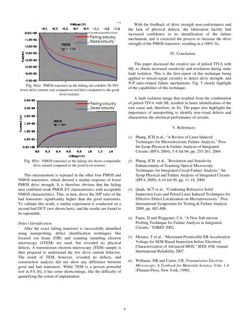
Fig. 8(a): PMOS transistor in the failing site exhibits 20-30%<br />
lower drive current (see comparison red line) compared to the good<br />
level restorer.<br />
Fig. 8(b): NMOS transistor in the failing site shows comparable<br />
drive current compared to the good level restorer.<br />
This measurement is repeated in the other four PMOS <strong>and</strong><br />
NMOS transistors, which showed a similar response of lower<br />
PMOS drive strength. It is therefore obvious that the failing<br />
area exhibited weak PMOS I/V characteristics with acceptable<br />
NMOS characteristics. This, in turn, drove the N/P ratio of the<br />
bad transistors significantly higher than the good transistors.<br />
To validate this result, a similar experiment is conducted on a<br />
second bad DUT (not shown here), <strong>and</strong> the results are found to<br />
be repeatable.<br />
Defect Identification<br />
After the exact failing transistor is successfully identified<br />
using nanoprobing, defect identification techniques like<br />
focused ion beam (FIB) <strong>and</strong> scanning tunneling electron<br />
microscopy (STEM) are used, but revealed no physical<br />
defects. A transmission electron microscopy (TEM) sample is<br />
then prepared to underst<strong>and</strong> the low drive current behavior.<br />
The result of TEM, however, revealed no defects, <strong>and</strong><br />
construction analysis did not show any difference between<br />
good <strong>and</strong> bad transistors. While TEM is a proven powerful<br />
tool in FA [6], it has some shortcomings, like the difficulty of<br />
quantifying the extent of implantation.<br />
4<br />
With the feedback of drive strength non-conformance <strong>and</strong><br />
the lack of physical defects, the fabrication facility had<br />
increased confidence in its identification of the failure<br />
mechanism, <strong>and</strong> it corrected the process to increase the drive<br />
strength of the PMOS transistor, resulting in a 100% fix.<br />
IV. Conclusion<br />
This paper discussed the creative use of pulsed <strong>TIVA</strong> with<br />
SIL to obtain increased sensitivity <strong>and</strong> resolution during static<br />
fault isolation. This is the first report of this technique being<br />
applied to mixed-signal circuitry to detect drive strength- <strong>and</strong><br />
N-P ratio-related failure mechanisms. Fig. 5 clearly highlight<br />
of the capabilities of this technique.<br />
A fault isolation image that resulted from the combination<br />
of pulsed <strong>TIVA</strong> with SIL resulted in faster identification of the<br />
root cause <strong>and</strong>, therefore, its fix. The paper also highlights the<br />
importance of nanoprobing to identify non-visual defects <strong>and</strong><br />
characterize the electrical performance of circuits.<br />
V. References<br />
[1] Phang, JCH et al., “A Review of Laser Induced<br />
Techniques for Microelectronic Failure Analysis,” Proc<br />
Int Symp Physical & Failure Analysis of Integrated<br />
Circuits (IPFA 2004), 5-8 Jul 04, pp. 255-261, 2004.<br />
[2] Phang, JCH et al., "<strong>Resolution</strong> <strong>and</strong> Sensitivity<br />
Enhancements of Scanning Optical Microscopy<br />
Techniques for Integrated Circuit Failure Analysis,” Int<br />
Symp Physical <strong>and</strong> Failure Analysis of Integrated Circuits<br />
(IPFA 2009), 6-10 Jul 09, pp. 11-18, 2009.<br />
[3] Quah, ACT et al., “<strong>Combining</strong> Refractive Solid<br />
Immersion Lens <strong>and</strong> <strong>Pulsed</strong> Laser Induced Techniques for<br />
Effective Defect Localization on Microprocessors,” Proc<br />
<strong>International</strong> Symposium for Testing & Failure Analysis<br />
2008, pp. 402-406.<br />
[4] Faure, D <strong>and</strong> Waggoner, CA, “A New Sub-micron<br />
Probing Technique for Failure Analysis in Integrated<br />
Circuits,” ESREF 2002.<br />
[5] Mizuno, T et al., “Maximum Permissible EB Acceleration<br />
Voltage for SEM-Based Inspection before Electrical<br />
Characterization of Advanced MOS,” IEEE 45th Annual<br />
<strong>International</strong> Reliability 2007.<br />
[6] Williams, DB <strong>and</strong> Carter, CB, Transmission Electron<br />
Microscopy: A Textbook for Materials Science, Vols. 1-4<br />
(Plenum Press, New York, 1996).