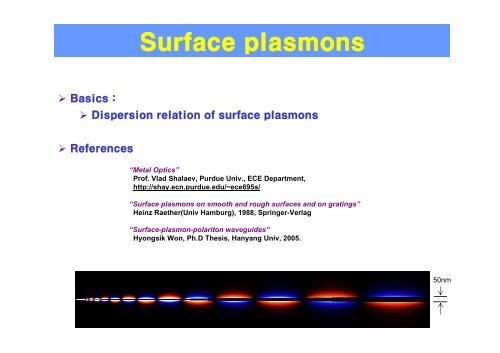
Surface plasmons
Surface plasmons
Surface plasmons

Create successful ePaper yourself
Turn your PDF publications into a flip-book with our unique Google optimized e-Paper software.
Basics :<br />
Dispersion relation of surface <strong>plasmons</strong><br />
References<br />
<strong>Surface</strong> <strong>plasmons</strong><br />
“Metal Optics”<br />
Prof. Vlad Shalaev, Purdue Univ., ECE Department,<br />
http://shay.ecn.purdue.edu/~ece695s/<br />
“<strong>Surface</strong> <strong>plasmons</strong> on smooth and rough surfaces and on gratings”<br />
Heinz Raether(Univ Hamburg), 1988, Springer-Verlag<br />
“<strong>Surface</strong>-plasmon-polariton waveguides”<br />
Hyongsik Won, Ph.D Thesis, Hanyang Univ, 2005.<br />
50nm
Metal Optics: An introduction<br />
Photonic functionality based on metals?!
What is a plasmon?<br />
Note: SP is a TM wave!
Plasmon-Polaritons<br />
Plasma oscillation = density fluctuation of free electrons<br />
+ + +<br />
- - -<br />
k<br />
+ - +<br />
Plasmons in the bulk oscillate at ω p determined by<br />
the free electron density and effective mass<br />
2<br />
Ne<br />
mε<br />
Plasmons confined to surfaces that can interact<br />
with light to form propagating “surface plasmon<br />
polaritons (SPP)”<br />
Confinement effects result in resonant SPP modes<br />
in nanoparticles<br />
2<br />
drude 1 Ne<br />
ω particle<br />
3 mε<br />
=<br />
ω<br />
drude<br />
p<br />
=<br />
0<br />
0
Local field intensity depends on wavelength<br />
(small propagation constant, k) (large propagation constant, k)
Dielectric constant of metal : Drude model<br />
σω ( )<br />
εEFF ( ω) = εB+<br />
i<br />
εω o<br />
= ε + i<br />
1 ⎛ σ ⎞<br />
= ε + i<br />
σ (1 + iωτ)<br />
B<br />
o<br />
⎜ ⎟<br />
ε oω⎝1 − iωτ<br />
⎠<br />
B<br />
o<br />
2 2<br />
εoω(1 + ω τ )<br />
B<br />
2 2<br />
ωτ p<br />
2 2 i<br />
2 2<br />
ωτ p<br />
3 3<br />
⎛ ⎞ ⎛ ⎞<br />
= ⎜ε− +<br />
⎜<br />
⎟ ⎜ ⎟<br />
1+<br />
ωτ ⎟ ⎜ωτ+ ωτ ⎟<br />
⎝ ⎠ ⎝ ⎠<br />
σ<br />
ne<br />
2<br />
2 o<br />
where, ω p = = : bulk plasma frequency ( ∼10<br />
eV for metal)<br />
ετ o εome<br />
Plasma frequency
Ideal case : metal as a free-electron gas<br />
• no decay (γ 0 : infinite relaxation time)<br />
• no interband transitions (ε B = 1)<br />
σ ( ω)<br />
εEFF ( ω) = εB+<br />
i<br />
εω<br />
o<br />
2 2 2 2 2<br />
⎛ ω pτ ⎞ ⎛ ωpτ ⎞ ⎛ ω ⎞<br />
τ →∞<br />
p<br />
= ⎜εB − + i<br />
⎯⎯⎯→ ε 1<br />
2 2 3 3 ε B = 1 EFF = −<br />
⎜<br />
⎟ ⎜ ⎟ ⎜ 2 ⎟<br />
1+<br />
ω τ ⎟ ⎜ωτ + ω τ ⎟ ⎜ ω ⎟<br />
⎝ ⎠ ⎝ ⎠ ⎝ ⎠<br />
ε<br />
r<br />
ω<br />
2<br />
p<br />
2<br />
= 1−<br />
0<br />
ω
<strong>Surface</strong>-<strong>plasmons</strong><br />
on dielectric-metal boundaries
Dispersion relation for EM waves in electron gas (bulk <strong>plasmons</strong>)<br />
• Dispersion relation:<br />
ω = ω(<br />
k)
Dispersion relation for surface <strong>plasmons</strong><br />
Exm Exd<br />
ε d<br />
ε m<br />
Z > 0<br />
Z < 0<br />
TM wave<br />
• At the boundary (continuity of the tangential E x , H y , and the normal D z ):<br />
= Hym = Hyd<br />
ε mEzm = ε dEzd
Dispersion relation for surface plasmon polaritons<br />
k H = ωε E<br />
zi<br />
yi<br />
i<br />
xi<br />
k H = ωε E<br />
zm<br />
k<br />
ε<br />
ym<br />
m<br />
k H =<br />
ωε E<br />
zd<br />
yd<br />
xm<br />
Exm = Exd<br />
Hym = Hyd<br />
k<br />
zm zd H ym = H yd<br />
m ε d<br />
( −ikziH<br />
yi,<br />
0,<br />
ikxiH<br />
yi )<br />
d<br />
xd<br />
( −iωε<br />
iE<br />
xi,<br />
0,<br />
−iωε<br />
iE<br />
zi )<br />
k k<br />
=<br />
ε ε<br />
zm zd<br />
m d
Dispersion relation for surface plasmon polaritons<br />
• For any EM wave:<br />
2<br />
2 ⎛ω⎞ 2 2<br />
= εi = x + zi x ≡ xm = xd<br />
k ⎜ ⎟ k k , where k k k<br />
⎝ c ⎠<br />
SP Dispersion Relation<br />
k<br />
x<br />
ω<br />
=<br />
c<br />
ε mεd ε + ε<br />
m d
<strong>Surface</strong> plasmon dispersion relation: relation<br />
ω<br />
p<br />
1+<br />
ε<br />
ω<br />
ω p<br />
d<br />
ω = ω + ck<br />
2 2 2 2<br />
p x<br />
ck x<br />
z<br />
ε<br />
d<br />
Dielectric:<br />
ε d<br />
x<br />
Metal: εm = ε '<br />
m +<br />
ε "<br />
m<br />
k<br />
x<br />
ω ⎛ ε ⎞ mε<br />
d =<br />
⎜<br />
⎟<br />
c ⎝ ε m + ε d ⎠<br />
1/<br />
2<br />
Radiative modes<br />
(ε'm > 0)<br />
Quasi-bound modes<br />
(−εd < ε'm < 0)<br />
Bound modes<br />
(ε' m < −ε d )<br />
k<br />
zi<br />
Re k x<br />
⎛ 2<br />
εi<br />
1/2<br />
⎞<br />
⎝εm + εd<br />
⎠<br />
ω<br />
= ⎜ ⎟<br />
c<br />
real k x<br />
real k z<br />
imaginary k x<br />
real k z<br />
real k x<br />
imaginary k z
X-ray wavelengths at optical frequencies !!<br />
λ vac=360 nm<br />
SiO2 Ag<br />
Very small<br />
SP wavelength
Excitation of surface <strong>plasmons</strong>
<strong>Surface</strong>-plasmon-polariton waveguides<br />
Ssurface plasmon polaritons<br />
propagating along very-thin(~ 10 nm) metal strips<br />
Dielectric – ε 3<br />
Metal – ε 2<br />
Dielectric – ε 1
When the film thickness becomes finite.<br />
mode<br />
overlap
Possibility of Propagation Range Extension<br />
frequency<br />
in-plane wavevector<br />
Long-Range SP:<br />
weak surface confinement, low loss<br />
Short-Range SP:<br />
strong surface confinement, high loss
Several 1 cm long, 15 nm thin and 8 micron wide gold stripes guiding LRSPPs<br />
3-6 mm long control electrodes<br />
low driving powers (approx. 100 mW) and high extinction ratios (approx. 30 dB)<br />
response times (approx. 0.5 ms)<br />
total (fiber-to-fiber) insertion loss of approx. 8 dB when using single-mode fibers
Fundamental symmetric mode of a metal stripe : thickness (T)<br />
14nm<br />
W=10um<br />
16nm<br />
T<br />
LR-SP WG<br />
18nm 20nm
P. Berini, PhotonicWest 2005.
(Spectalis Co.)
Tunable Wavelength filter by direct heating a metal wire<br />
Polymer 2<br />
INPUT OUTPUT<br />
+ -<br />
Polymer 1<br />
Substrate<br />
Transmittance (dB)<br />
-40<br />
-45<br />
-50<br />
-55<br />
-60<br />
-65<br />
-70<br />
1544.1<br />
1540 1545 1550 1555 1560<br />
W avelength (nm )<br />
1558.3
Vertical directional couplers<br />
H. Won, APL vol.88, 011110 (2006)
Variable optical attenuator based on LR-SPP<br />
Submitted to EL, S. Park & S. Song
Localized <strong>Surface</strong> Plasmons :<br />
Nanofocusing and Nanolithography<br />
ω (10 15 s -1 )<br />
8<br />
6<br />
4<br />
2<br />
ω=c k x<br />
λ=337 nm; ε 1 = -1<br />
Broad<br />
dispersion<br />
0<br />
0 20 40 60 80 100<br />
k x (μm -1 )<br />
'<br />
1<br />
At large kx<br />
( ε1 →−ε2), z i ≈ .<br />
kx<br />
E = ± iE ( air : + i, metal :- i)<br />
z x<br />
Strong confinement at the interface<br />
Nano focusing
Propose metal nanowires.<br />
Beam radius -> zero!<br />
Propagation Loss<br />
(asymmetric mode)<br />
High
Asymmetric mode : field enhancement at a metallic tip<br />
Er Er Ez M. I. Stockman, “Nanofocusing of Optical Energy in Tapered Plasmonic Waveguides,” Phys. Rev. Lett. 93, 137404 (2004)]<br />
50nm<br />
E z<br />
* See MOVIES : SPP propagation through a metallic tip
2007/5/1 ~<br />
an optical range resonator based on single mode metal-insulator-metal plasmonic gap waveguides.<br />
A small bridge between the resonator and the input waveguide can be used to tune the resonance frequency.<br />
FDTD with the perfectly matched layer boundary conditions
Plasmonic Crystal Demultiplexer and Multiports<br />
the realization of two-dimensional optical wavelength demultiplexers and multiports for surface <strong>plasmons</strong><br />
polaritons (SPPs) based on plasmonic crystals, i.e., photonic crystals for SPPs.
Slow Propagation, Anomalous Absorption, and Total External Reflection<br />
of <strong>Surface</strong> Plasmon Polaritons in Nanolayer Systems<br />
n=2<br />
n=1<br />
n=0
we show how the dispersion relation of surface plasmon polaritons (SPPs) propagating along a perfectly conducting wire can be tailored by<br />
corrugating its surface with a periodic array of radial grooves.<br />
Importantly, the propagation characteristics of these spoof SPPs can be controlled by the surface geometry, opening the way to important<br />
applications such as energy concentration on cylindrical wires and superfocusing using conical structures.
Summary : Plasmonic Photonics<br />
Plasmonics: the next chip-scale technology<br />
Plasmonics is an exciting new device technology that has recently emerged.<br />
A tremendous synergy can be attained by integrating plasmonic, electronic, and conventional dielectric photonic devices<br />
on the same chip and taking advantage of the strengths of each technology.<br />
Plasmonic devices,<br />
therefore, might interface naturally with similar speed photonic devices<br />
and similar size electronic components. For these reasons, plasmonics<br />
may well serve as the missing link between the two device<br />
technologies that currently have a difficult time communicating. By<br />
increasing the synergy between these technologies, plasmonics may be<br />
able to unleash the full potential of nanoscale functionality and<br />
become the next wave of chip-scale technology.