Workshop on Nanostructured Graphene - CMT group - Universiteit ...
Workshop on Nanostructured Graphene - CMT group - Universiteit ...
Workshop on Nanostructured Graphene - CMT group - Universiteit ...

You also want an ePaper? Increase the reach of your titles
YUMPU automatically turns print PDFs into web optimized ePapers that Google loves.
Organizers:<br />
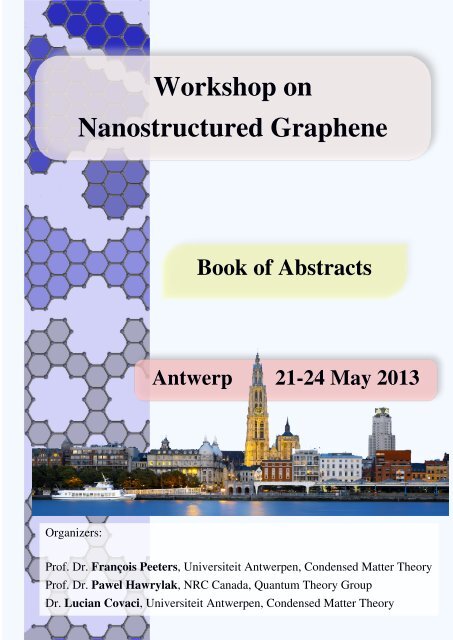
<str<strong>on</strong>g>Workshop</str<strong>on</strong>g> <strong>on</strong><br />
<strong>Nanostructured</strong> <strong>Graphene</strong><br />
Book of Abstracts<br />
Antwerp<br />
21st-24th May 2013<br />
Antwerp 21-24 May 2013<br />
Prof. Dr. François Peeters, <strong>Universiteit</strong> Antwerpen, C<strong>on</strong>densed Matter Theory<br />
Prof. Dr. Pawel Hawrylak, NRC Canada, Quantum Theory Group<br />
Dr. Lucian Covaci, <strong>Universiteit</strong> Antwerpen, C<strong>on</strong>densed Matter Theory
Supported by:<br />
European Science Foundati<strong>on</strong><br />
(Eurocores project: Euro<strong>Graphene</strong>)<br />
Flemish Science Foundati<strong>on</strong><br />
Scientific Research Communities (WOG):<br />
- Computati<strong>on</strong>al modelling of materials<br />
- Tuning the functi<strong>on</strong>al properties of nanoparticles and nanowires<br />
University of Antwerp
Programme of the workshop <strong>on</strong> nanostructured graphene<br />
Antwerp, 21 st -24 th May 2013<br />
Tuesday 21 May Wednesday 22 May Thursday 23 May Friday 24 May Time<br />
Registrati<strong>on</strong> 8.30 – 9.00<br />
L. Vandersypen M. Morgenstern C. Stampfer J. Folk 9.00 - 10.00<br />
F. Amet P. Potasz S. Yuan M. C<strong>on</strong>nolly 10.00 - 10.30<br />
Coffee Break Coffee Break Coffee Break Coffee Break 10.30 - 11.00<br />
E. Andrei K. Ensslin A. Geim A.-P. Jauho 11.00 – 12.00<br />
B. Trauzettel D. Guclu V. Pereira A. Chaves 12.00 - 12.45<br />
Lunch & discussi<strong>on</strong>s Lunch & discussi<strong>on</strong>s Lunch & discussi<strong>on</strong>s Lunch & discussi<strong>on</strong>s 12.45 – 14.15<br />
S. Ulloa J. Fernandez-Rossier R. Egger M. Neek-Amal 14.15 – 15.00<br />
T. Chakraborty G. Burkard J. McGuire L. Covaci 15.00 – 15.45<br />
Coffee Break &<br />
Poster sessi<strong>on</strong> 1<br />
Coffee Break &<br />
Poster sessi<strong>on</strong> 2<br />
Visit historical<br />
Antwerp<br />
C<strong>on</strong>ference dinner<br />
(Hof van Liere)<br />
End of workshop<br />
15:30<br />
15.45 – 17.45<br />
20.00 – 22.00<br />
55 + 5 mins<br />
40 + 5 mins<br />
25 + 5 mins
Tuesday May 21 2013<br />
Sessi<strong>on</strong>: Morning sessi<strong>on</strong><br />
Part 1: Invited talks<br />
9:00 - 10:00 Lieven Vandersypen, Delft Technical University, Netherlands<br />
Ballistic transport in CVD and natural graphene<br />
10:00 - 10:30 Francois Amet, Stanford University, USA<br />
Insulating behavior in m<strong>on</strong>olayer graphene <strong>on</strong> bor<strong>on</strong>-nitride<br />
10:30 - 11:00 Coffee Break<br />
11:00 - 12:00 Eva Andrei, Rutgers University, USA<br />
Screening Charged Impurities in <strong>Graphene</strong>: From Cloaking to Supercriticality<br />
12:00 - 12:45 Björn Trauzettel, University of Wuerzburg, Germany<br />
Transport properties of graphene nanostructures<br />
12:45 - 14:15 Lunch and discussi<strong>on</strong>s<br />
Sessi<strong>on</strong>: Afterno<strong>on</strong> sessi<strong>on</strong><br />
14:15 - 15:00 Sergio Ulloa, Ohio University, USA<br />
Spin Scattering in <strong>Graphene</strong>: Impurity Characterizati<strong>on</strong> and Birefringent Electr<strong>on</strong><br />
Optics<br />
15:00 - 15:45 T. Chakraborty, University of Manitoba, Canada<br />
Novel physics of interacting Dirac fermi<strong>on</strong>s in a quantizing magnetic field<br />
15:45-17:45 Coffee Break and Poster Sessi<strong>on</strong> 1
Wednesday May 22 2013<br />
Sessi<strong>on</strong>: Morning sessi<strong>on</strong><br />
9:00 - 10:00 Markus Morgenstern, RWTH Aachen, Germany<br />
Probing <strong>Graphene</strong> <strong>on</strong> the Nanoscale by Scanning Tunneling Microcopy<br />
10:00 - 10:30 Pawel Potasz: Wroclaw University of Technology, Poland<br />
Electr<strong>on</strong>ic and magnetic properties of triangular graphene quantum dots and<br />
rings<br />
10:30 - 11:00 Coffee Break<br />
11:00 - 12:00 Klaus Ensslin, ETH Zürich, Switzerland<br />
<strong>Graphene</strong> nanodevices with reduced disorder<br />
12:00 - 12:45 Devrim Guclu, Izmir Institute of Technology, Turkey<br />
Optical and electrical c<strong>on</strong>trol of magnetic properties of graphene quantum<br />
dots and Mobius nanoribb<strong>on</strong> rings<br />
12:45 - 14:15 Lunch and discussi<strong>on</strong>s<br />
Sessi<strong>on</strong>: Afterno<strong>on</strong> sessi<strong>on</strong><br />
14:15 - 15:00 Joaquin Fernadez-Rossier, Iberian Nanotechnology Laboratory, Spain<br />
Anisotropic intrinsic spin relaxati<strong>on</strong> in graphene<br />
15:00 - 15:45 Guido Burkard, University of K<strong>on</strong>stanz, Germany<br />
Spin and valley in graphene quantum dots<br />
15:45-17:45 Coffee Break and Poster Sessi<strong>on</strong> 2
Thursday May 23 2013<br />
Sessi<strong>on</strong>: Morning sessi<strong>on</strong><br />
9:00 - 10:00 Christoph Stampfer, RWTH Aachen, Germany<br />
Progresses in etched graphene quantum dots<br />
10:00 - 10:30 Shengjun Yuan, Radboud University, Netherlands<br />
Modeling Electr<strong>on</strong>ic, Optical and Magnetic Properties of <strong>Graphene</strong><br />
10:30 - 11:00 Coffee Break<br />
11:00 - 12:00 Andre Geim, Manchester University, UK<br />
Some interacti<strong>on</strong>, magnetic and superlattice effects in graphene<br />
12:00 - 12:45 Vitor Pereira, Nati<strong>on</strong>al University of Singapore, Singapore<br />
Res<strong>on</strong>ant tunneling in graphene pseudomagnetic quantum dots<br />
12:45 - 14:15 Lunch and discussi<strong>on</strong>s<br />
Sessi<strong>on</strong>: Afterno<strong>on</strong> sessi<strong>on</strong><br />
14:15 - 15:00 Reinhold Egger, University of Dusseldorf, Germany<br />
Str<strong>on</strong>gly interacting Dirac fermi<strong>on</strong>s in graphene quantum dots<br />
15:00 - 15:45 John McGuire, Michigan State University, USA<br />
Excit<strong>on</strong>ic Interacti<strong>on</strong>s in Colloidal <strong>Graphene</strong> Quantum Dots<br />
15:45-17:45 Visit historical Antwerp<br />
20:00-22:00 C<strong>on</strong>ference dinner at the University Club: Hof van Liere
Friday May 24 2013<br />
Sessi<strong>on</strong>: Morning sessi<strong>on</strong><br />
9:00 - 10:00 Josh Folk, University of British Columbia, Canada<br />
Defect-Mediated Spin Relaxati<strong>on</strong> in <strong>Graphene</strong><br />
10:00 - 10:30 Malcolm R. C<strong>on</strong>nolly, Nati<strong>on</strong>al Physical Laboratory, UK<br />
Rapid time-c<strong>on</strong>trolled emissi<strong>on</strong> of single Dirac fermi<strong>on</strong>s from graphene quantum<br />
dots<br />
10:30 - 11:00 Coffee Break<br />
11:00 - 12:00 Antti-Pekka Jauho, Technical University of Denmark, Denmark<br />
Transport in nanostructured graphene<br />
12:00 - 12:45 Andrey Chaves, Universidade Federal do Ceara, Brazil<br />
Wave packet dynamics in graphene: strain effects, edge scattering and valley filtering<br />
12:45- 14:15 Lunch and discussi<strong>on</strong>s<br />
Sessi<strong>on</strong>: Afterno<strong>on</strong> sessi<strong>on</strong><br />
14:15 - 14:45 Mehdi Neek-Amal, <strong>Universiteit</strong> Antwerpen, Belgium<br />
Bor<strong>on</strong> nitride m<strong>on</strong>olayer under n<strong>on</strong>-uniform strain<br />
14:45 - 15:15 Lucian Covaci, <strong>Universiteit</strong> Antwerpen, Belgium<br />
Andreev quantum dots in graphene<br />
15:30 End of the workshop
Abstracts of invited talks
Ballistic transport in CVD and natural graphene<br />
Lieven Vandersypen ∗<br />
Kavli Institute of Nanoscience, TU Delft<br />
We will present unpublished and recently published work <strong>on</strong> transport measurements<br />
of graphene devices in the ballistic regime. Most recently, we have observed<br />
transverse magnetic focussing in micr<strong>on</strong> size Hall bars created from single layer<br />
CVD graphene. The synthesis is d<strong>on</strong>e under highly c<strong>on</strong>trolled c<strong>on</strong>diti<strong>on</strong>s, resulting<br />
in single crystals with up to 0.5 mm in lateral dimensi<strong>on</strong>s, and electr<strong>on</strong> mobilities<br />
over 100.000 cm 2 /Vs at 4K (<strong>on</strong> hBN). For the first time, ballistic transport over<br />
1 µm was observed in CVD graphene. Comparis<strong>on</strong> of atomic force microscopy<br />
and transport measurements indicate that when wrinkles are present, they spoil<br />
ballistic transport. Earlier, we have created split-gate bilayer graphene devices<br />
(using graphene exfoliated from natural graphite), sandwiched in between hBN dielectrics.<br />
Transport through electrostatically induced c<strong>on</strong>stricti<strong>on</strong>s shows signs of<br />
quantized c<strong>on</strong>ductance, also a signature of ballistic transport. Transport through<br />
two c<strong>on</strong>stricti<strong>on</strong>s in series shows clear Coulomb blockade at low temperature.<br />
Finally, Coulomb blockade was observed even at room temperature, in devices<br />
created by the c<strong>on</strong>trolled rupture of a graphene sheet subjected to a large electr<strong>on</strong><br />
current in air. The size of the quantum dot islands is estimated to be in the 1 nm<br />
range, giving additi<strong>on</strong> energies up to 1.6 eV.<br />
Measurements and sample fabricati<strong>on</strong> were carried out by Victor Calado,<br />
Stijn Goossens and Amelia Barreiro. CVD graphene was synthesized by Shou-En<br />
Zhou in the <strong>group</strong> of Guido Janssen (TU Delft).<br />
[1] Ballistic transport in CVD graphene. In preparati<strong>on</strong>.<br />
[2] Gate defined zero- and <strong>on</strong>e-dimensi<strong>on</strong>al c<strong>on</strong>finement in bilayer graphene, A.M.<br />
Goossens, S.C.M. Driessen, T.A. Baart, K. Watanabe, T. Taniguchi, L.M.K. Vandersypen,<br />
Nano letters 12 , 4656 (2012).<br />
[3] Quantum Dots at Room Temperature Carved out from Few-Layer <strong>Graphene</strong>,<br />
A. Barreiro, H. S. J. van der Zant, and L. M. K. Vandersypen, Nano Lett. 12,<br />
6096 (2012).<br />
∗ Electr<strong>on</strong>ic address: l.m.k.vandersypen@tudelft.nl
Insulating behavior in m<strong>on</strong>olayer graphene <strong>on</strong><br />
bor<strong>on</strong>-nitride<br />
Francois Amet ∗ and David Goldhaber-Gord<strong>on</strong> †<br />
Stanford University<br />
The c<strong>on</strong>ductivity at the neutrality point in m<strong>on</strong>olayer graphene is known to<br />
saturate <strong>on</strong> the order of e 2 /h due to disorder-induced density-fluctuati<strong>on</strong>s. In<br />
this study, in c<strong>on</strong>trast, we observed a diverging peak resistivity in high-mobility<br />
graphene devices with a bor<strong>on</strong>-nitride substrate and a suspended top-gate. At low<br />
temperature, the peak resistivity under the top-gate increases by three orders of<br />
magnitude and becomes as high as several megohms. In a perpendicular magnetic<br />
field, the device remains insulating and directly transiti<strong>on</strong>s to the ν = 0 quantum<br />
Hall phase. We discuss the roles of substrate-induced valley symmetry-breaking<br />
and external screening of density fluctuati<strong>on</strong>s by the top-gate as causes of our<br />
observati<strong>on</strong>s.<br />
∗ Electr<strong>on</strong>ic address: amet@stanford.edu<br />
† Electr<strong>on</strong>ic address: goldhaber-gord<strong>on</strong>@stanford.edu
Screening Charged Impurities in <strong>Graphene</strong>:<br />
From Cloaking to Supercriticality<br />
Eva Y. Andrei ∗<br />
Rutgers Unversity<br />
We study a charged impurity in graphene and its screening by the Dirac electr<strong>on</strong>s<br />
in the presence of a magnetic field. Using scanning tunneling microscopy<br />
and spectroscopy we show that the effective charge of the impurity can be tuned<br />
by employing a gate voltage to c<strong>on</strong>trol the occupancy of Landau levels. At low<br />
occupancy str<strong>on</strong>g screening by the c<strong>on</strong>ducti<strong>on</strong> electr<strong>on</strong>s renders the impurity essentially<br />
invisible. Screening progressively diminishes with increased occupancy<br />
until, for fully occupied Landau-levels, the unscreened impurity significantly perturbs<br />
the spectrum in its vicinity, lifting the orbital degeneracy and causing the<br />
Landau-levels to split into discrete states. In this regime the impurity displays signatures<br />
of supercritical behavior associated with electr<strong>on</strong>ic orbits collapsing into<br />
its core. Thus the magnetic field makes it possible to tune the strength of interacti<strong>on</strong>s<br />
from subcritical to supercritical, providing direct experimental access to<br />
Coulomb criticality.<br />
∗ Electr<strong>on</strong>ic address: eandrei@physics.rutgers.edu
Transport properties of graphene nanostructures<br />
Björn Trauzettel ∗<br />
Würzburg University, Germany<br />
We discuss transport properties of nanostructured graphene, for instance,<br />
graphene nanoribb<strong>on</strong>s and graphene rings. In our theoretical analysis, these systems<br />
are either coupled to normal metal or to superc<strong>on</strong>ducting electr<strong>on</strong> reservoirs.<br />
We discover interesting fingerprints of graphene-specific physics. Particularly, we<br />
will present a color-dependence of the c<strong>on</strong>ductance in disordered graphene due<br />
to adatoms as well as the possibility to distinguish specular from retro Andreev<br />
reflecti<strong>on</strong> in graphene rings coupled to <strong>on</strong>e normal metal and <strong>on</strong>e superc<strong>on</strong>ducting<br />
lead.<br />
∗ Electr<strong>on</strong>ic address: trauzettel@physik.uni-wuerzburg.de
Spin Scattering in <strong>Graphene</strong>: Impurity<br />
Characterizati<strong>on</strong> and Birefringent Electr<strong>on</strong><br />
Optics<br />
Mahmoud M. Asmar ∗ and Sergio E. Ulloa †<br />
Ohio University and Freie Universitat Berlin<br />
An important element <strong>on</strong> the dynamics of spins in materials is the spin-orbit<br />
interacti<strong>on</strong> (SOI), which reflects/arises from intrinsic lack of inversi<strong>on</strong> symmetry<br />
in the lattice structure, or via broken symmetries in the system due to external<br />
or interfacial fields (Rashba interacti<strong>on</strong>). Although intrinsic SOI is weak in<br />
graphene, the Rashba SOI can in fact be large due to str<strong>on</strong>g local hybridizati<strong>on</strong>s<br />
by impurities of defects or by manipulati<strong>on</strong> of substrates or applied gates [1]. We<br />
have studied electr<strong>on</strong>/hole transport in graphene under sizeable SOI and address<br />
theoretically some of the anticipated observables due to this effect.<br />
We have developed analytical spinor soluti<strong>on</strong>s of the Dirac equati<strong>on</strong> that include<br />
spin dependent observables, and use these to examine the role of SOI <strong>on</strong> scattering<br />
cross secti<strong>on</strong>s. By calculating the ratio of total to transport cross secti<strong>on</strong> at low<br />
energy we are able to probe the degree of isotropy of the scattering processes,<br />
and c<strong>on</strong>sequently probe the nature of the impurities and defects present in the<br />
graphene sample. We show that at low energies, this ratio of cross secti<strong>on</strong>s<br />
(equivalent to the ratio of scattering times obtainable from experiments) can be<br />
nearly 1 (instead of 2, as expected with no SOI), to a degree that depends <strong>on</strong> the<br />
Rashba SOI strength. This suggests then a sample specific measurement of the<br />
important effective size of the SOI, especially if <strong>on</strong>e is to c<strong>on</strong>sider spin transport.<br />
We also show that Rashba SOI in graphene gives rise to optical birefringence<br />
in electr<strong>on</strong> optics, which in essence reflects the intrinsic crystal structure even<br />
at l<strong>on</strong>g electr<strong>on</strong>ic wavelengths. This effect requires the presence of Rashba SOI,<br />
where different <strong>group</strong> velocities depend <strong>on</strong> the chirality of the electr<strong>on</strong>ic states,<br />
mimicking the light polarizati<strong>on</strong> dependence of the <strong>group</strong> velocities in optical<br />
birefringent materials. This can in principle be achieved via gated regi<strong>on</strong>s, and<br />
result in the formati<strong>on</strong> of spinful cusps and caustics caused by the Veselago<br />
lens defined by the gate. Interestingly, this would be evident by the doubling of<br />
caustics and cusps produced by circular birefringent lenses, where the spacing<br />
∗ Electr<strong>on</strong>ic address: MA236408@ohio.edu<br />
† Electr<strong>on</strong>ic address: ulloa@ohio.edu
etween the two different chiral cusps is proporti<strong>on</strong>al to the strength of the<br />
Rashba interacti<strong>on</strong> in the system [2].<br />
[1] D. Marchenko et al., Nature Commun. 3, 1232 (2012).<br />
[2] M. M. Asmar and S. E. Ulloa, Phys. Rev. B 87, 075420 (2013).
Novel physics of interacting Dirac fermi<strong>on</strong>s in a<br />
quantizing magnetic field<br />
Tapash Chakraborty ∗<br />
University of Manitoba, Winnipeg, Canada<br />
The relativistic-like behavior of electr<strong>on</strong>s in graphene exhibits novel interacti<strong>on</strong>induced<br />
properties in a quantizing magnetic field. Here <strong>on</strong>e observes many intriguing<br />
properties of the fracti<strong>on</strong>al quantum Hall effect states that are absent<br />
in c<strong>on</strong>venti<strong>on</strong>al (n<strong>on</strong>-relativistic) semic<strong>on</strong>ductor systems. In bilayer graphene the<br />
interacti<strong>on</strong> strength can be c<strong>on</strong>trolled by a bias voltage and by the orientati<strong>on</strong> of<br />
the magnetic field. The finite bias voltage between the graphene m<strong>on</strong>olayers can<br />
in fact, enhance the interacti<strong>on</strong> strength in a given Landau level. As a functi<strong>on</strong> of<br />
the bias voltage, a graphene bilayer system shows transiti<strong>on</strong>s from a state of weak<br />
electr<strong>on</strong>-electr<strong>on</strong> interacti<strong>on</strong>s to a state with str<strong>on</strong>g interacti<strong>on</strong>s. Interestingly,<br />
the in-plane comp<strong>on</strong>ent of a tilted magnetic field can also alter the interacti<strong>on</strong><br />
strength in bilayer graphene. Tuning of the interacti<strong>on</strong> strength of Dirac fermi<strong>on</strong>s<br />
in graphene therefore provides a unique route to a profound understanding of interacting<br />
fermi<strong>on</strong>s in a magnetic field. The nature of the Pfaffian state in bilayer<br />
graphene will also be discussed and shown that the stability of this state can be<br />
greatly enhanced by applying an in-plane magnetic field.<br />
∗ Electr<strong>on</strong>ic address: tapash@physics.umanitoba.ca
Probing <strong>Graphene</strong> <strong>on</strong> the Nanoscale by Scanning<br />
Tunneling Microcopy<br />
Markus Morgenstern ∗<br />
Institute of Physics and JARA-FIT, RWTH Aachen, D. 52074 Aachen, Germany<br />
We use ultra-high-vacuum scanning tunneling microscopy at low temperature<br />
(6 K) to probe basic features of graphene relevant to mechanical and quantum<br />
mechanical applicati<strong>on</strong>s.<br />
Firstly, I present wave functi<strong>on</strong> mapping in graphene quantum dots deposited<br />
<strong>on</strong> Ir(111) [1]. The quantum dots are c<strong>on</strong>fined exclusively by zig-zag edges. However,<br />
edge states are absent due to an exchange interacti<strong>on</strong> of the π-bands of<br />
graphene with the dz2 surface states of the Ir(111) [2]. The exchange interacti<strong>on</strong><br />
gets c<strong>on</strong>tinuously smaller away from the edges, which leads to weak c<strong>on</strong>finement<br />
of the quantum dot states being decisive for a rather regular wave functi<strong>on</strong> shape<br />
observed experimentally. The wave functi<strong>on</strong>s are additi<strong>on</strong>ally influenced by the<br />
penetrati<strong>on</strong> of an sp-like surface state of Ir(111) into graphene [1]. C<strong>on</strong>cerning<br />
the edge state, DFT calculati<strong>on</strong>s reveal that H-terminated graphene nanoribb<strong>on</strong>s<br />
<strong>on</strong> Au(111) should exhibit magnetic edge states [3]. First experiments will be<br />
shown. Sec<strong>on</strong>dly, the mechanical properties of graphene flakes deposited by the<br />
scotch tape method are probed by STM. The graphene is partly not c<strong>on</strong>formal to<br />
the substrate, but provides areas which are freely suspended [4]. The valleys of<br />
this corrugati<strong>on</strong> can be further lifted by the van-der Waals forces and the electrostatic<br />
forces of the tip of the STM [5]. During c<strong>on</strong>tinuous lifting, we often observe<br />
a breaking of atomic symmetry, i.e. the atomic structure switches reproducibly<br />
between a hexag<strong>on</strong>al and a triangular appearance.<br />
[1] D. Subramaniam et al., Phys. Rev. Lett. 108 (2012) 046801.<br />
[2] Y. Li et al., Adv. Materials, 25, 1967 (2013).<br />
[3] Y. Li et al., arXiv:1210.2876.<br />
[4] V. Geringer et al., Phys. Rev. Lett. 102 (2009) 076102.<br />
[5] T. Mashoff et al., Nano. Lett. 10 (2010) 461.<br />
∗ Electr<strong>on</strong>ic address: mmorgens@physik.rwth-aachen.de
Electr<strong>on</strong>ic and magnetic properties of triangular<br />
graphene quantum dots and rings<br />
Pawel Potasz ∗<br />
Institute of Physics, Wroclaw University of Technology<br />
The theory of electr<strong>on</strong>ic and magnetic properties of triangular graphene quantum<br />
dots (TGQD) and rings (TGQR) with zigzag edges is presented. Single particle<br />
properties are investigated using the tight-binding model and the effect of<br />
electr<strong>on</strong>-electr<strong>on</strong> interacti<strong>on</strong>s are treated using both mean-field Hubbard model<br />
and a combinati<strong>on</strong> of tight-binding, Hartree-Fock, and c<strong>on</strong>figurati<strong>on</strong> interacti<strong>on</strong>s<br />
methods (tb+HF+CI). We show that TGQDs break symmetry between the two<br />
sublattices of a graphene bipartite h<strong>on</strong>eycomb lattice, which leads to an appearance<br />
of a shell of degenerate states at the Fermi level Ef = 0 in the middle of<br />
the energy gap [1-6]. We derive an analytical form of the eigenfuncti<strong>on</strong>s corresp<strong>on</strong>ding<br />
to the zero-energy shell and analyze shell degeneracy as a functi<strong>on</strong> of<br />
size of TGQDs and width of TGQRs [5,6]. The stability with respect to disorder<br />
and the influence of the external magnetic field is c<strong>on</strong>sidered [5, 7, 8]. Next, the<br />
total spin and electr<strong>on</strong>ic correlati<strong>on</strong>s are investigated using tb+HF+CI method.<br />
We show that for the charge neutral TGQD, the degenerate shell is half-filled and<br />
the electr<strong>on</strong>-electr<strong>on</strong> interacti<strong>on</strong>s lead to the appearance of a finite magnetic moment<br />
[1-9]. This result is c<strong>on</strong>sistent with Lieb’s theorem for a Hubbard model<br />
<strong>on</strong> a bipartite lattice [10]. Using mean-field Hubbard model, we analyze width<br />
and size dependence of the magnetic moment in TGQR. The stability of the magnetic<br />
properties in TGQD and TGQR with respect to shell filling c<strong>on</strong>trolled by<br />
the external gate is investigated using tb+HF+CI [4, 9]. We show that both the<br />
many-body energy gap and total spin oscillates as a functi<strong>on</strong> of the filling fracti<strong>on</strong>.<br />
In particular, spin polarized ground state at half-filling is depolarized by additi<strong>on</strong><br />
of a single electr<strong>on</strong> for TGQDs of sizes below a critical size. The effect of electr<strong>on</strong>ic<br />
correlati<strong>on</strong>s <strong>on</strong> Coulomb and Spin blockade in transport through a TGQD<br />
are discussed [4].<br />
Collaborators: A. Guclu, O. Voznyy, M. Korkusinski, and P. Hawrylak.<br />
[1] M. Ezawa, Phys. Rev. B 76, 245415 (2007).<br />
[2] J. Fernandez-Rossier and J. J. Palacios, Phys. Rev. Lett. 99, 177204 (2007).<br />
[3] W. L. Wang, S. Meng, and E. Kaxiras, Nano Letters 8, 241 (2008).<br />
[4] A. D. Güçlü, P. Potasz, O. Voznyy, M. Korkusinski, and P. Hawrylak, Phys.<br />
Rev. Lett. 103, 246805 (2009).<br />
∗ Electr<strong>on</strong>ic address: pawel.potasz@pwr.wroc.pl
[5] P. Potasz, A. D. Güçlü, and P. Hawrylak, Phys. Rev. B 81, 033403 (2010).<br />
[6] P. Potasz, A. D. Güçlü, and P. Hawrylak, Phys. Rev. B 83, 174441 (2011).<br />
[7] M. Ezawa, Physica E 42 , 703 (2010).<br />
[8] O.Voznyy, A. D. Güçlü, P. Potasz and P. Hawrylak, Phys. Rev. B 83, 165417<br />
(2011).<br />
[9] P. Potasz, A. D. Güçlü, A. Wojs, and P. Hawrylak, Phys. Rev. B 85, 075431<br />
(2012).<br />
[10] E. H. Lieb, Phys. Rev. Lett. 62, 1201 (1989).
<strong>Graphene</strong> nanodevices with reduced disorder<br />
Klaus Ensslin ∗<br />
ETH Zurich<br />
<strong>Graphene</strong> quantum devices, such as nanoribb<strong>on</strong>s, quantum rings and quantum<br />
dots often display electr<strong>on</strong>ic properties which are governed by disorder potentials<br />
arising from bulk and edge c<strong>on</strong>tributi<strong>on</strong>s.<br />
In order to reduce bulk disorder, single layer graphene micr<strong>on</strong>-sized devices and<br />
nanoribb<strong>on</strong>s have been fabricated <strong>on</strong> hexag<strong>on</strong>al bor<strong>on</strong> nitride substrates. These<br />
micr<strong>on</strong>-sized devices have significantly higher mobility and lower disorder density<br />
compared to devices fabricated <strong>on</strong> silic<strong>on</strong> dioxide substrate in agreement with previous<br />
findings. The transport characteristics of the reactive-i<strong>on</strong>-etched graphene<br />
nanoribb<strong>on</strong>s <strong>on</strong> hexag<strong>on</strong>al bor<strong>on</strong> nitride, however, appear to be very similar to<br />
those of ribb<strong>on</strong>s <strong>on</strong> a silic<strong>on</strong> dioxide substrate. A detailed study reveals both similarities<br />
as well as differences between the two types of devices. This suggests that<br />
the edges have an important influence <strong>on</strong> transport in reactive-i<strong>on</strong>-etched graphene<br />
nanodevices. In an alternative approach with the goal to minimize edge disorder<br />
graphene quantum structures are prepared <strong>on</strong> bilayer graphene. Using a homogeneous<br />
back gate and a nanostructured top gate energy gaps can be locally induced<br />
into the bilayer graphene. This way the edges are determined by electrostatics and<br />
possibly screening in graphene which should lead to smoother edges compared to<br />
etched samples.<br />
This work was d<strong>on</strong>e in collaborati<strong>on</strong> with D. Bischoff, A. Varlet, P. Sim<strong>on</strong>et, C.<br />
Barraud and T. Ihn.<br />
∗ Electr<strong>on</strong>ic address: ensslin@phys.ethz.ch
Optical and electrical c<strong>on</strong>trol of magnetic<br />
properties of graphene quantum dots and<br />
Mobius nanoribb<strong>on</strong> rings<br />
A. Devrim Güçlü ∗<br />
Izmir Institute of Technology, Izmir, Turkey<br />
We present a theory of optical, magnetic and topological properties of graphene<br />
quantum dots and graphene Möbius strips using numerical techniques combining<br />
tight-binding, Hartree-Fock and c<strong>on</strong>figurati<strong>on</strong> interacti<strong>on</strong>s methods. Triangular<br />
graphene quantum dots with zigzag edges [1-6] exhibit robust magnetic moment<br />
and optical transiti<strong>on</strong>s simultaneously in the THz, visible and UV spectral ranges<br />
due to the existence of a band of degenerate states lying at the Fermi level. The<br />
magnetic and optical properties [3-6] are determined by str<strong>on</strong>g electr<strong>on</strong>-electr<strong>on</strong><br />
and excit<strong>on</strong>ic interacti<strong>on</strong>s. We show that the magnetizati<strong>on</strong> of the zigzag edges can<br />
be manipulated optically. The magnetic moment can be first erased by additi<strong>on</strong><br />
of a single electr<strong>on</strong> spin with a gate, then restored by absorpti<strong>on</strong> of a phot<strong>on</strong>.<br />
The c<strong>on</strong>versi<strong>on</strong> of a single phot<strong>on</strong> to a magnetic moment results in a many-body<br />
effect, optical spin blockade. In graphene Möbius nanoribb<strong>on</strong> rings [7], the finite<br />
width opens a gap and n<strong>on</strong>trivial topology of the Möbius ring leads to a single<br />
edge with an induced, effective gauge field, in analogy to topological insulators.<br />
The single zigzag edge leads to a shell of degenerate states at the Fermi level<br />
and a ferromagnetic (FM) ground state at half-filling, due to electr<strong>on</strong>-electr<strong>on</strong><br />
interacti<strong>on</strong>s. For fracti<strong>on</strong>al fillings, the magnetic moment is found to oscillate as<br />
a functi<strong>on</strong> of the shell filling.<br />
Collaborators: P. Potasz, I. Özfidan, O. Voznyy, M. Korkusinski, M. Grabowski<br />
and P. Hawrylak.<br />
[1] J. Fernandez-Rossier, and J. J. Palacios, Phys. Rev. Lett. 99, 177204 (2007).<br />
[2] M. Ezawa, Phys. Rev. B 76, 245415 (2007).<br />
[3] A. D. Güçlü, P. Potasz, O. Voznyy, M. Korkusinski, and P. Hawrylak, Phys<br />
Rev. Lett. 103, 246805 (2009).<br />
[4] A. D. Güçlü, P. Potasz, and P. Hawrylak, Phys. Rev. B, 82, 155445 (2010).<br />
[5] P. Potasz, A. D. Güçlü, A. Wojs,P. Hawrylak, Phys. Rev. B 85, 075431<br />
(2012).<br />
[6] A. D. Güçlü, P Hawrylak, Phys. Rev. B 87, 035425 (2013).<br />
[7] A. D. Güçlü, M Grabowski, P Hawrylak, Phys. Rev. B 85, 035435 (2013).<br />
∗ Electr<strong>on</strong>ic address: devrimguclu@iyte.edu.tr
Anisotropic intrinsic spin relaxati<strong>on</strong> in graphene<br />
J. Fernandez-Rossier ∗ and D. Gosalbez<br />
Internati<strong>on</strong>al Iberian Nanotechnology Laboratory (INL), Braga, Portugal and<br />
Universidad de Alicante, Alicante, Spain<br />
P. Merodio-Camara and S. Fratini<br />
Institut Neel, CNRS, Grenoble, France<br />
In this talk I discuss an intrinsic spin scattering mechanism in graphene originated<br />
by the interplay of atomic spin-orbit interacti<strong>on</strong> and the local curvature<br />
induced by flexural distorti<strong>on</strong>s of the atomic lattice. Starting from a multiorbital<br />
tight-binding Hamilt<strong>on</strong>ian with spin-orbit coupling c<strong>on</strong>sidered n<strong>on</strong>-perturbatively,<br />
we derive an effective Hamilt<strong>on</strong>ian for the spin scattering of the Dirac electr<strong>on</strong>s<br />
due to flexural distorti<strong>on</strong>s. We compute the spin lifetime due to flexural ph<strong>on</strong><strong>on</strong>s<br />
and we find values in the microsec<strong>on</strong>d range at room temperature. Interestingly,<br />
these spin lifetimes are anisotropic <strong>on</strong> two counts. First, they are different for<br />
different spin quantizati<strong>on</strong> axis. Sec<strong>on</strong>d, they depend <strong>on</strong> the in-plane momentum<br />
directi<strong>on</strong> of the initial state. Our results set upper limits for the spin lifetimes<br />
in graphene that will be dominant if extrinsic sources of spin relaxati<strong>on</strong> can be<br />
removed from the samples.<br />
∗ Electr<strong>on</strong>ic address: joaquin.fernandez-rossier@inl.int
Spin and valley in graphene quantum dots<br />
Guido Burkard ∗<br />
University of K<strong>on</strong>stanz, Germany<br />
<strong>Graphene</strong> has emerged as an interesting material for coherent spin physics and<br />
spin qubits, due to the low c<strong>on</strong>centrati<strong>on</strong> of nuclear spins and relatively weak spinorbit<br />
coupling. However, the localizati<strong>on</strong> of electr<strong>on</strong>s in quantum dots in graphene<br />
is a n<strong>on</strong>-trivial task due to the absence of a band gap and the related effect of Klein<br />
tunneling [1]. Am<strong>on</strong>g the possible soluti<strong>on</strong>s to this problem are electrostatically<br />
defined quantum dots in armchair graphene nanoribb<strong>on</strong>s [2] or gapped graphene<br />
[3]. Interestingly, the valley degeneracy present in graphene modifies the spin-orbit<br />
induced spin relaxati<strong>on</strong> [4,5] as well as hyperfine interacti<strong>on</strong> with C-13 nuclear spins<br />
and plays an important role in the spin-valley blockade in double quantum dots<br />
[6]. The exchange coupling in graphene mixes spin and valley degrees of freedom<br />
and calls for special procedures for spin-based quantum informati<strong>on</strong> processing [7].<br />
[1] M. I. Katsnels<strong>on</strong>, K. S. Novoselov, A. K. Geim, Nature Phys. 2, 620 (2006).<br />
[2] B. Trauzettel, D. Bulaev, D. Loss, and GB, Nature Phys. 3, 192 (2007).<br />
[3] P. Recher, J. Nilss<strong>on</strong>, GB, and B. Trauzettel, Phys. Rev. B 79, 085407<br />
(2009).<br />
[4] P. R. Struck and GB, Phys. Rev. B 82, 125401 (2010).<br />
[5] M. Droth and GB, Phys. Rev. B 84, 155404 (2011).<br />
[6] A. Palyi and GB, Phys. Rev. B 80, 201404 (2009).<br />
[7] N. Rohling and GB, New Journal of Physics 14, 083008 (2012).<br />
∗ Electr<strong>on</strong>ic address: Guido.Burkard@uni-k<strong>on</strong>stanz.de
Progresses in etched graphene quantum dots<br />
Christoph Stampfer ∗<br />
JARA-FIT and II. Institute of Physics B,<br />
RWTH Aachen, 52074 Aachen, Germany<br />
<strong>Graphene</strong> quantum dots are interesting and promising systems for studying l<strong>on</strong>gliving<br />
spin states of c<strong>on</strong>fined electr<strong>on</strong>s. In particular nanostructured graphene<br />
quantum devices based <strong>on</strong> (reactive i<strong>on</strong>) etching processes have been studied extensively<br />
in the last few years. In these quantum devices, Coulomb blockade, excited<br />
states, spin states and electr<strong>on</strong>-hole crossover have been successfully dem<strong>on</strong>strated.<br />
However, due to bulk disorder and edge roughness the behavior of all these devices<br />
is irregular and c<strong>on</strong>trol proves to be a challenge [1-2].<br />
Here we report our recent progress <strong>on</strong> quantum transport studies <strong>on</strong> etched<br />
graphene quantum dots. In particular, we focus <strong>on</strong> graphene quantum dots with<br />
highly tunable tunneling barriers, which allow for the first time pulse-gated transient<br />
current spectroscopy measurements of excited states. These experiments<br />
provide insights to relaxati<strong>on</strong> times of c<strong>on</strong>fined electr<strong>on</strong>s in graphene and allow us<br />
to extract a lower limit of the charge relaxati<strong>on</strong> rates <strong>on</strong> the order of 60-100 ns<br />
[3]. Furthermore, we show a detailed analysis of transport measurements taken <strong>on</strong><br />
etched graphene quantum dots resting <strong>on</strong> hexag<strong>on</strong>al bor<strong>on</strong> nitride substrates. In<br />
agreement with earlier experiments we find that nanostructures with dimensi<strong>on</strong>s<br />
smaller 150 nm are str<strong>on</strong>gly limited by edge roughness. C<strong>on</strong>sequently an improvement<br />
of the substrate induced disorder is not helping to improve the overall device<br />
performance. Finally, we report <strong>on</strong> recent progress <strong>on</strong> a disorder potential reducing<br />
edge functi<strong>on</strong>alizati<strong>on</strong> of graphene nanodevices.<br />
[1] B. Terres, J. Dauber, C. Volk, S. Trellenkamp, U. Wichmann, and C.<br />
Stampfer, Appl. Phys. Lett. 98, 032109 (2011)<br />
[2] C. Volk, S. Fringes, B. Terrs, J. Dauber, S. Engels, S. Trellenkamp, and C.<br />
Stampfer, Nano Lett. 11, 3581 (2011)<br />
[3] C. Volk, C. Neumann, S. Kazarski, S. Fringes, S. Engels, F. Haupt, A. Mueller,<br />
and C. Stampfer, Nature Communicati<strong>on</strong> DOI: 10.1038/ncomms2738, in press<br />
(2013).<br />
∗ Electr<strong>on</strong>ic address: stampfer@physik.rwth-aachen.de
Modeling Electr<strong>on</strong>ic, Optical and Magnetic<br />
Properties of <strong>Graphene</strong><br />
Shengjun Yuan ∗ and Mikhail I. Katsnels<strong>on</strong><br />
Institute for Molecules and Materials, Radboud University of Nijmegen,<br />
NL-6525AJ, Nijmegen, The Netherlands<br />
One of the most important problems in graphene is to understand the influence<br />
of disorder <strong>on</strong> its physical properties. Motivated by recent experiments, we<br />
performed a systemic study of the electr<strong>on</strong>ic, optical and magnetic properties<br />
of single-layer, multilayer and nanostructured graphene [1-12], including different<br />
types of imperfecti<strong>on</strong> such as vacancies, adatoms, admolecules, ripples, puddles<br />
and coulomb impurities.<br />
The methods are based <strong>on</strong> the numerical simulati<strong>on</strong>s of electr<strong>on</strong>s in the framework<br />
of full pi-band tight-binding model, without diag<strong>on</strong>alizati<strong>on</strong> of the Hamilt<strong>on</strong>ian<br />
matrix. The density of states is calculated by the time-evoluti<strong>on</strong> method,<br />
which is based <strong>on</strong> the simulati<strong>on</strong> of wave packet evoluti<strong>on</strong> according to the timedependent<br />
Schrdinger equati<strong>on</strong>, with additi<strong>on</strong>al averaging over random superpositi<strong>on</strong><br />
of basis states. We extend the time-evoluti<strong>on</strong> method by using the Kubo<br />
formula to the calculati<strong>on</strong> of polarizati<strong>on</strong> functi<strong>on</strong>, dielectric functi<strong>on</strong>, resp<strong>on</strong>se<br />
functi<strong>on</strong>, energy loss functi<strong>on</strong>, electr<strong>on</strong>ic and magnetic susceptibility, static and<br />
dynamical (optical) c<strong>on</strong>ductivity, diffusi<strong>on</strong> coefficients, mean free path, localizati<strong>on</strong><br />
length, charge velocity and mobility. The magnetic field is introduced by<br />
means of the Peierls substituti<strong>on</strong>, and the effect of electr<strong>on</strong>-electr<strong>on</strong> interacti<strong>on</strong><br />
is c<strong>on</strong>sidered within the random phase approximati<strong>on</strong>. The Klein tunneling and<br />
quantum interference are studied by direct simulati<strong>on</strong> of the wave packet propagati<strong>on</strong>.<br />
Our numerical methods allow us to carry out calculati<strong>on</strong>s for rather large<br />
systems, up to hundreds of milli<strong>on</strong>s of atoms, with a computati<strong>on</strong>al effort that<br />
increases <strong>on</strong>ly linearly with the system size.<br />
[1] S. Yuan, H. De Raedt, and M. I. Katsnels<strong>on</strong>, Phys. Rev. B 82, 115448 (2010).<br />
[2] S. Yuan, H. De Raedt, and M. I. Katsnels<strong>on</strong>, Phys. Rev. B 82, 235409 (2010).<br />
[3] S. Yuan, R. Roldn, and M. I. Katsnels<strong>on</strong>, Phys. Rev. B 84, 035439 (2011).<br />
[4] S. Yuan, R. Roldn, and M. I. Katsnels<strong>on</strong>, Phys. Rev. B 84, 125455 (2011).<br />
[5] S. Yuan, R. Roldn, and M. I. Katsnels<strong>on</strong>, Solid State Comm. 152, 1446<br />
(2012).<br />
[6] S. Yuan et al, Phys. Rev. B 84, 195418 (2011).<br />
∗ Electr<strong>on</strong>ic address: s.yuan@science.ru.nl
[7] S. Yuan et al, Phys. Rev. Lett. 109, 156601 (2012).<br />
[8] S. Yuan et al, Phys. Rev. B 87, 085430 (2013).<br />
[9] A. Singha et al, Science 332, 1176 (2011).<br />
[10] T. O. Wehling et al, Phys. Rev. Lett. 105, 056802 (2010).<br />
[11] R. R. Nair et al, Small 6, 2877 (2010).<br />
[12] M. A. Akhukov et al, New J. of Phys. 14, 123012 (2012).
Some interacti<strong>on</strong>, magnetic and superlattice<br />
effects in graphene<br />
∗ Electr<strong>on</strong>ic address: andre.k.geim@manchester.ac.uk<br />
André Geim ∗<br />
University of Manchester
Res<strong>on</strong>ant tunneling in graphene pseudomagnetic<br />
quantum dots<br />
Vitor M. Pereira ∗<br />
Nati<strong>on</strong>al University of Singapore<br />
Endowed with the str<strong>on</strong>gest covalent b<strong>on</strong>ding in nature, graphene exhibits the<br />
largest tensi<strong>on</strong>al strength ever registered (E ≈ 1 TPa), and a record range of<br />
elastic deformati<strong>on</strong> for a crystal, which can be as high as 15-20 %. Such outstanding<br />
mechanical characteristics are complemented by an unusual coupling of<br />
lattice deformati<strong>on</strong>s to the electr<strong>on</strong>ic moti<strong>on</strong>, that can be captured by the c<strong>on</strong>cept<br />
of a fictitious or pseudo-magnetic field (PMF) arising as a result of n<strong>on</strong>-uniform<br />
local changes in the electr<strong>on</strong>ic hopping amplitudes. Since electr<strong>on</strong>s in graphene<br />
resp<strong>on</strong>d to these local PMFs as they would to a real magnetic field, this specific<br />
strain-induced perturbati<strong>on</strong> is not screened by the free electr<strong>on</strong>s in the same<br />
way that the usual displacement field coupling can be. C<strong>on</strong>sequently, the ability<br />
to manipulate the strain distributi<strong>on</strong> in graphene opens the enticing prospect<br />
of strain-engineering its electr<strong>on</strong>ic and optical properties, as well as of enhancing<br />
interacti<strong>on</strong> and correlati<strong>on</strong> effects. The recent experimental c<strong>on</strong>firmati<strong>on</strong> that<br />
PMFs in the striking range 300-600 T are possible with sp<strong>on</strong>taneously occurring<br />
deformati<strong>on</strong>s in structures spanning <strong>on</strong>ly a few nm brings this prospect of str<strong>on</strong>gly<br />
impacting graphenes electr<strong>on</strong>ic properties by strain closer to fruiti<strong>on</strong>.<br />
Despite this recent experimental evidence for str<strong>on</strong>g PMF-induced Landau quantizati<strong>on</strong><br />
and various studies addressing implicati<strong>on</strong>s of PMF for the graphene electr<strong>on</strong>ic<br />
spectrum, the nature (and opportunities) of electr<strong>on</strong>ic transport in such<br />
nanostructures remains scarcely explored. In this c<strong>on</strong>text a combinati<strong>on</strong> of analytical,<br />
numerical, and simulati<strong>on</strong> approaches will be used to describe features<br />
of quantum transport in a representative situati<strong>on</strong> where tailored local strain distributi<strong>on</strong>s<br />
are used to c<strong>on</strong>fine electr<strong>on</strong>s at the nanoscale. The fact that local<br />
n<strong>on</strong>-uniform strain manifests itself as a PMF in graphene which can easily exceed<br />
100 T opens the prospect for local pseudo-magnetic c<strong>on</strong>finement of carriers.<br />
This allows for analogues of magnetic quantum dots, where transport proceeds<br />
by res<strong>on</strong>ant tunneling assisted by Landau levels in the c<strong>on</strong>finement regi<strong>on</strong>, with<br />
the important difference that there is no real magnetic field, and the effect can<br />
be spatially restricted to a few nm. The transport characteristics of <strong>on</strong>e such<br />
strained pseudo-magnetic quantum dot structure in the y-juncti<strong>on</strong> geometry will<br />
be presented and discussed.<br />
∗ Electr<strong>on</strong>ic address: vpereira@nus.edu.sg
Str<strong>on</strong>gly interacting Dirac fermi<strong>on</strong>s in graphene<br />
quantum dots<br />
Reinhold Egger ∗<br />
University of Duesseldorf, Germany<br />
Low-energy quasi-particles in m<strong>on</strong>olayer graphene provide a realizati<strong>on</strong> of massless<br />
Dirac fermi<strong>on</strong>s in two spatial dimensi<strong>on</strong>s. Electr<strong>on</strong>-electr<strong>on</strong> interacti<strong>on</strong>s in<br />
that case should be quite str<strong>on</strong>g, with effective fine structure c<strong>on</strong>stant of order<br />
unity. Artificial atoms can then be formed by c<strong>on</strong>fining N quasiparticles (<strong>on</strong> top<br />
of the filled Dirac sea) in a quantum dot. We discuss the electr<strong>on</strong>ic structure<br />
and stability of this interacting N particle Dirac system. In particular, a finitesize<br />
versi<strong>on</strong> of the bulk excit<strong>on</strong>ic instability is predicted [1] and Wigner molecule<br />
formati<strong>on</strong> should be detectable [2].<br />
[1] T. Paananen and R. Egger, Phys. Rev. B 84, 155456 (2011) .<br />
[2] T. Paananen, R. Egger, and H. Siedentop, Phys. Rev. B 83, 085409 (2011).<br />
∗ Electr<strong>on</strong>ic address: egger@thphy.uni-duesseldorf.de
Excit<strong>on</strong>ic Interacti<strong>on</strong>s in Colloidal <strong>Graphene</strong><br />
Quantum Dots<br />
John A. McGuire ∗<br />
Department of Physics and Astr<strong>on</strong>omy, Michigan State University<br />
We present results of optical studies of single- and biexcit<strong>on</strong>s in graphene quantum<br />
dots (GQDs) c<strong>on</strong>sisting of 132 and 168 C atoms in fully aromatic structures,<br />
i.e., having no unpaired pz electr<strong>on</strong>s, and having HOMO-LUMO transiti<strong>on</strong>s of 1.6-<br />
1.8 eV. Bottom-up synthesis allows the creati<strong>on</strong> of such GQDs with well defined<br />
lattice structure.[1] GQDs of > 100 sp 2 hybridized C atoms are intriguing systems<br />
both for applicati<strong>on</strong>s in solar energy c<strong>on</strong>versi<strong>on</strong> and for fundamental studies of<br />
carrier interacti<strong>on</strong>s and dynamics in str<strong>on</strong>gly c<strong>on</strong>fined two-dimensi<strong>on</strong>al systems.<br />
We focus here <strong>on</strong> the earliest stages of the excit<strong>on</strong> lifetime after optical excitati<strong>on</strong>.<br />
Compared to traditi<strong>on</strong>al semic<strong>on</strong>ductor quantum dots, the weak screening associated<br />
with the two-dimensi<strong>on</strong>al lattice of C atoms leads to str<strong>on</strong>g carrier-carrier<br />
interacti<strong>on</strong>s. In both time-resolved photoluminescence and transient absorpti<strong>on</strong><br />
(TA) measurements of GQDs dispersed in toluene, we see fast cooling of carriers<br />
with electr<strong>on</strong>-hole pairs generated with >1 eV excess energy relaxing to the band<br />
edge within a few hundred femtosec<strong>on</strong>ds. Following initial cooling, we identify<br />
biexcit<strong>on</strong> binding energies of >200 meV for the lowest-energy optically accessible<br />
biexcit<strong>on</strong>s. Biexcit<strong>on</strong>s are expected to be short lived in such str<strong>on</strong>gly c<strong>on</strong>fined<br />
structures. In 380-nm l<strong>on</strong>g carb<strong>on</strong> nanotubes, n<strong>on</strong>radiative Auger recombinati<strong>on</strong><br />
of biexcit<strong>on</strong>s to a single excit<strong>on</strong> occurs <strong>on</strong> a timescale of ∼1 ps.[2] A naive linear<br />
scaling of Auger lifetime with nanotube length extended to the size of our GQDs<br />
would suggest a biexcit<strong>on</strong> lifetime of the order of 5 fs GQDs.[3] However, <strong>on</strong> increasing<br />
the excitati<strong>on</strong> intensity from the single- to multi-phot<strong>on</strong>-absorpti<strong>on</strong> regime, we<br />
observe the emergence of dynamics <strong>on</strong> the ∼300 fs timescale. Excitati<strong>on</strong>-fluencedependence<br />
of this comp<strong>on</strong>ent suggests that Auger recombinati<strong>on</strong> of biexcit<strong>on</strong>s in<br />
our GQDs occurs <strong>on</strong> a ∼300 fs timescale.<br />
[1] Yan, X.; Cui, X.; Li, L. S., Synthesis of Large, Stable Colloidal <strong>Graphene</strong><br />
Quantum Dots with Tunable Size. J. Am. Chem. Soc. 2010, 132, 5944-5945.<br />
[2] Wang, F.; Dukovic, G.; Knoesel, E.; Brus, L. E.; Heinz, T. F., Observati<strong>on</strong><br />
of Rapid Auger Recombinati<strong>on</strong> in Optically Excited Semic<strong>on</strong>ducting Carb<strong>on</strong><br />
Nanotubes. Phys. Rev. B 2004, 70, 241403.<br />
[3] Wang, F.; Wu, Y.; Hybertsen, M. S.; Heinz, T. F., Auger Recombinati<strong>on</strong> of<br />
Excit<strong>on</strong>s in One-Dimensi<strong>on</strong>al Systems. Phys. Rev. B 2006, 73, 245424.<br />
∗ Electr<strong>on</strong>ic address: mcguire@pa.msu.edu
Defect-Mediated Spin Relaxati<strong>on</strong> in <strong>Graphene</strong><br />
Josh Folk<br />
University of British Columbia ∗<br />
This talk with describe a transport measurement that disentangles mechanisms<br />
of spin and orbital phase relaxati<strong>on</strong> in graphene. The measurement is based<br />
<strong>on</strong> well-known quantum interference phenomena–weak localizati<strong>on</strong> and universal<br />
c<strong>on</strong>ductance fluctuati<strong>on</strong>s. We show that a careful analysis of the in-plane magnetic<br />
field and temperature dependences of these effects can separately quantify<br />
spin-orbit and magnetic scattering rates; this technique works especially well in<br />
graphene due to its single-atom thickness. Spin relaxati<strong>on</strong> in exfoliated graphene<br />
<strong>on</strong> SiO2 is found to be dominated by magnetic scattering (scattering off of magnetic<br />
defects), with a smaller c<strong>on</strong>tributi<strong>on</strong> from in-plane spin-orbit interacti<strong>on</strong>. A<br />
similar measurement is performed in graphene <strong>on</strong> SiC; interestingly, both magnetic<br />
scattering and spin-orbit interacti<strong>on</strong> are a factor of 10 str<strong>on</strong>ger than in exfoliated<br />
graphene.<br />
∗ Electr<strong>on</strong>ic address: jfolk@physics.ubc.ca
Rapid time-c<strong>on</strong>trolled emissi<strong>on</strong> of single Dirac<br />
fermi<strong>on</strong>s from graphene quantum dots<br />
M. R. C<strong>on</strong>nolly, ∗ S. P. Giblin, M. Kataoka, and J. D. Fletcher<br />
Nati<strong>on</strong>al Physical Laboratory, UK<br />
K. L. Chiu, C. Chua, J. P. Griffiths, and G. A. C. J<strong>on</strong>es<br />
University of Cambridge, UK<br />
V. I. Fal’ko<br />
University of Lancaster, UK<br />
C. G. Smith<br />
University of Cambridge<br />
T. J. B. M. Janssen<br />
Nati<strong>on</strong>al Physical Laboratory<br />
Electr<strong>on</strong>ic excitati<strong>on</strong>s in undoped m<strong>on</strong>olayer graphene behave dynamically like<br />
chiral massless Dirac fermi<strong>on</strong>s. Electrical transport measurements traditi<strong>on</strong>ally<br />
probe the unique nature of scattering, interference, and localizati<strong>on</strong> of these quasiparticles<br />
by driving randomly generated wavepackets through a graphene layer and<br />
m<strong>on</strong>itoring the evoluti<strong>on</strong> of the time-averaged current density with magnetic field,<br />
temperature, and carrier c<strong>on</strong>centrati<strong>on</strong>. In this work we describe a different mechanism<br />
for generating currents which is based <strong>on</strong> the time-c<strong>on</strong>trolled release of single<br />
charge-quantized excitati<strong>on</strong>s from lithographically defined graphene quantum dots<br />
[1]. The applicati<strong>on</strong> of phase-shifted radiofrequency signals to all-graphene side<br />
gates results in a single charge being transferred between the dots each cycle, generating<br />
a net current equal to the fundamental electr<strong>on</strong>ic charge times the drive<br />
frequency [2]. Quantized charge transfer is observed up to GHz frequencies, an<br />
order of magnitude higher than previously achieved using c<strong>on</strong>venti<strong>on</strong>al metallic or<br />
semic<strong>on</strong>ductor adiabatic charge pumps. We discuss the role played by the physical<br />
and electr<strong>on</strong>ic properties of graphene in facilitating such efficient charge transfer,<br />
the character of the emitted wavepacket, and the c<strong>on</strong>formity of the experimental<br />
data to theoretical models based <strong>on</strong> adiabatic transfer through metallic islands<br />
[3]. High-speed emissi<strong>on</strong> of tailorable wavepackets provides the foundati<strong>on</strong>s for exploring<br />
and manipulating the quantum nature of individual electr<strong>on</strong>ic excitati<strong>on</strong>s<br />
in graphene, paving the way towards single Dirac fermi<strong>on</strong> quantum optics [4] and<br />
read-out of spin-based graphene qubits for quantum informati<strong>on</strong> processing [5].<br />
∗ Electr<strong>on</strong>ic address: mrc1@npl.co.uk
[1] M. R. C<strong>on</strong>nolly, et al., Nature Nanotechnology (2013) (in press);<br />
arXiv:1207.6597 (2012)<br />
[2] H. Pothier, et al., Europhysics Letters, 17(3) 249-254 (1992).<br />
[3] N. Winkler, et al., Phys. Rev. B 79, 235309 (2009).<br />
[4] E. Bocquill<strong>on</strong>, et al., Science 339, 1054 (2013).<br />
[5] B. Trauzettel, et al., Nature Phys. 3, 192-196 (2007).
Transport in nanostructured graphene<br />
Antti-Pekka Jauho ∗ and Mikkel Settnes †<br />
CNG - Center for <strong>Nanostructured</strong> <strong>Graphene</strong>, DTU Nanotech<br />
Stephen Power ‡<br />
CNG - Center for Nanostrcutured <strong>Graphene</strong>, DTU Nanotech<br />
We address two different situati<strong>on</strong>s. (1) Regular perforati<strong>on</strong>s of graphene with<br />
nanoscale holes (<strong>Graphene</strong> antidot lattices, GAL) can be used to locally modify<br />
the electr<strong>on</strong>ic structure, e.g., to introduce an energy gap [1]. Recent research has<br />
shown that it is possible to create phot<strong>on</strong>ic crystal-like electr<strong>on</strong> wave-guides in<br />
graphene by using GALs as the c<strong>on</strong>fining agent [2]. Here, we report <strong>on</strong> our recent<br />
simulati<strong>on</strong>s of such structures, employing a recursive Green’s functi<strong>on</strong> technique.<br />
We focus <strong>on</strong> two issues: the efficiency of the wave-guide in c<strong>on</strong>fining the electr<strong>on</strong><br />
wave-functi<strong>on</strong> for different Fermi energies, and the role of antidot disorder <strong>on</strong> the<br />
c<strong>on</strong>ductance profile of such systems. (2) We have developed a theoretical formulati<strong>on</strong><br />
to interpret measurements of the c<strong>on</strong>ductive properties of nanostructured<br />
graphene, using multiple STM-type probes. The situati<strong>on</strong> differs c<strong>on</strong>ceptually<br />
from the standard Landauer c<strong>on</strong>figurati<strong>on</strong>: instead of having a finite sample between<br />
(multiple) probes, we c<strong>on</strong>sider a large sample, but which is probed locally<br />
by several probes. This is a microscopic extensi<strong>on</strong> of the standard four-point spectroscopy<br />
[3]. Results will be presented for various geometries with <strong>on</strong>e fixed probe,<br />
with a local impurity (impurities), and a scannable sec<strong>on</strong>d probe.<br />
[1] T. G. Pedersen et al., Phys. Rev. Lett. 100, 136804 (2008).<br />
[2] J. G. Pedersen et al., Phys. Rev. B 86, 245410 (2012).<br />
[3] P. Boggild, et al, Rev. Sci. Instr., 71, 2781-2783 (2000).<br />
∗ Electr<strong>on</strong>ic address: Antti-Pekka.Jauho@nanotech.dtu.dk<br />
† Electr<strong>on</strong>ic address: mikse@nanotech.dtu.dk<br />
‡ Electr<strong>on</strong>ic address: spow@nanotech.dtu.dk
Wave packet dynamics in graphene: strain<br />
effects, edge scattering and valley filtering<br />
Andrey Chaves ∗<br />
Universidade Federal do Ceara, Brazil<br />
Theoretical models based <strong>on</strong> wave packet propagati<strong>on</strong> have been extensively applied<br />
in the study of transport properties of electr<strong>on</strong>s in low dimensi<strong>on</strong>al structures.<br />
In this work, we dem<strong>on</strong>strate the use of wave packet propagati<strong>on</strong> for the study of<br />
a series of interesting phenomena in m<strong>on</strong>olayer and bilayer graphene. The time<br />
evoluti<strong>on</strong> of the wave packet is calculated by means of a split-operator technique<br />
[1] adapted for the tight-binding Hamilt<strong>on</strong>ian describing electr<strong>on</strong>s in graphene, as<br />
well as for the Dirac Hamilt<strong>on</strong>ian for low energy electr<strong>on</strong>s in the c<strong>on</strong>tinuum model.<br />
We discuss how wave packets can be used to investigate several well known phenomena<br />
in graphene in greater details, such as Klein tunneling [2], zitterbewegung<br />
[3] and the inter- and intra-valley scattering in zigzag and armchair boundaries, respectively<br />
[4]. Most importantly, we will show how the dynamics of a wave packet<br />
have been used to predict other interesting effects in graphene, for example (i) the<br />
existence of a n<strong>on</strong>-propagating state in the armchair boundary of a strained m<strong>on</strong>olayer<br />
graphene nanoribb<strong>on</strong>, and the valley filtering (ii) by a quantum point c<strong>on</strong>tact<br />
in a bilayer graphene and (iii) by a m<strong>on</strong>olayer-bilayer [5] graphene juncti<strong>on</strong>.<br />
[1] A. Chaves et al., Phys. Rev. B 82, 205430 (2010);<br />
[2] J. M. Pereira Jr. et al., Semic<strong>on</strong>d. Sci. Technol. 25 033002 (2010);<br />
[3] T. M. Rusin and W. Zawadzki, Phys. Rev. B 80, 045416 (2009);<br />
[4] A. R. Akhmerov and C. W. J. Beenacker, Phys. Rev. B 77, 085423 (2008);<br />
[5] T. Nakanishi et al., Phys. Rev. B 82, 125428 (2010).<br />
∗ Electr<strong>on</strong>ic address: andrey@fisica.ufc.br
Bor<strong>on</strong> nitride m<strong>on</strong>olayer under inhomogeneous<br />
stress<br />
Mehdi Neek-Amal ∗<br />
<strong>Universiteit</strong> Antwerpen<br />
The electr<strong>on</strong>ic properties of a strained hexag<strong>on</strong>al bor<strong>on</strong>-nitride sheet are investigated<br />
using density functi<strong>on</strong>al theory and classical molecular dynamics simulati<strong>on</strong>s.<br />
Triaxial in-plane strain is applied to a hexag<strong>on</strong>al shaped bor<strong>on</strong>-nitride flake with<br />
zig-zag edges. Different from graphene, the triaxial strain localizes the molecular<br />
orbital close to the Fermi level in the center of the sheet depending <strong>on</strong> the type<br />
of edge atoms (i.e. B versus N). The energy gap decreases with increasing strain.<br />
We show how inhomogeneous strain <strong>on</strong> the bor<strong>on</strong>-nitride sheet can be used to<br />
selectively detect various gas molecules.<br />
∗ Electr<strong>on</strong>ic address: neekamal@srttu.edu
Andreev quantum dots in graphene<br />
Lucian Covaci ∗<br />
Department of Physics, <strong>Universiteit</strong> Antwerpen<br />
Although graphene is not intrinsically superc<strong>on</strong>ducting, Cooper pairs can diffuse<br />
from a superc<strong>on</strong>ducting c<strong>on</strong>tact. The superc<strong>on</strong>ducting proximity effect was<br />
observed experimentally in graphene Josephs<strong>on</strong> juncti<strong>on</strong>s with c<strong>on</strong>tacts made of<br />
various superc<strong>on</strong>ducting materials like Al, Pb, Nb and even layered materials like<br />
NbSe2 [1,2]. When the energy of the electr<strong>on</strong>s in the graphene layer is below the<br />
superc<strong>on</strong>ducting gap of the c<strong>on</strong>tacts, they will be bound in the normal regi<strong>on</strong>.<br />
These are the well known Andreev bound states. We c<strong>on</strong>sider a graphene layer<br />
deposited <strong>on</strong> top of a rough superc<strong>on</strong>ducting surface such that the graphene layer<br />
can be c<strong>on</strong>sidered to be partially freestanding and strained. It was recently shown<br />
that strain has a peculiar effect <strong>on</strong> the electr<strong>on</strong>ic properties in graphene, namely<br />
that it will coupled exactly like a gauge field [3,4]. Under certain c<strong>on</strong>diti<strong>on</strong>s it is<br />
thus possible to have str<strong>on</strong>g pseudo-magnetic fields and even pseudo-Landau levels<br />
coexisting with superc<strong>on</strong>ducting correlati<strong>on</strong>s [5]. By using an efficient numerical<br />
method [6] we solve the Bogoliubov-de Gennes equati<strong>on</strong>s for a tight binding model<br />
of the graphene layer. Deformati<strong>on</strong>s of the graphene layer are c<strong>on</strong>sidered as Gaussian<br />
bumps around imperfecti<strong>on</strong>s of the substrate. We show that in the regi<strong>on</strong>s<br />
where the sheet is freestanding, bound states due to Andreev reflecti<strong>on</strong>s appear.<br />
[1] H. B. Heersche, P. Jarillo-Herrero, J. B. Oostinga, L. M. K. Vandersypen,<br />
and A. F. Morpurgo, Nature (L<strong>on</strong>d<strong>on</strong>) 446, 56 (2007).<br />
[2] A. Kanda, T. Sato, H. Goto, H. Tomori, S. Takana, Y. Ootuka, and K.<br />
Tsukagoshi, Physica C 470, 1477 (2010).<br />
[3] F. Guinea, M. I. Katsnels<strong>on</strong>, and A. K. Geim, Nat. Phys. 6, 30 (2009).<br />
[4] N. Levy, S. A. Burke, K. L. Meaker, M. Panlasigui, A. Zettl, F. Guinea, A.<br />
H. C. Neto, and M. F. Crommie, Science 329, 544 (2010).<br />
[5] L. Covaci and F. M. Peeters, Phys. Rev. B 84, 241401(R) (2011).<br />
[6] L. Covaci, F. M. Peeters, and M. Berciu, Phys. Rev. Lett. 105, 167006<br />
(2010).<br />
∗ Electr<strong>on</strong>ic address: lucian@covaci.org
Abstracts of poster presentati<strong>on</strong>s
Part 2: C<strong>on</strong>tributed poster presentati<strong>on</strong>s<br />
Poster Sessi<strong>on</strong> 1 ( Tuesday - 21 May)<br />
P01. Z. Ao Electric field induced hydrogenati<strong>on</strong> of graphene<br />
P02. S. Ulloa Doping dependence of K<strong>on</strong>do states in bilayer graphene<br />
P03. S. Barraza-Lopez Strain-engineering of graphene electr<strong>on</strong>ic structure bey<strong>on</strong>d c<strong>on</strong>tinuum elasticity<br />
P04. G. R. Berdiyorov Structural properties and stability of silic<strong>on</strong> clusters intercalated bilayer graphene<br />
P05. B. Beschoten Spin transport in single and bilayer graphene<br />
P06. C. De Beule Gapless interface states at the juncti<strong>on</strong> between two topological insulators<br />
P07. P. Butti Efficiency of graphene based rectifiers<br />
P08. P. Clark <strong>Graphene</strong> Quantum Point C<strong>on</strong>tacts in the Ballistic Regime<br />
P09. S. Costamagna Life-time of acoustic ph<strong>on</strong><strong>on</strong> modes in <strong>Graphene</strong><br />
P10. M. Droth Electr<strong>on</strong> Spin Relaxati<strong>on</strong> in <strong>Graphene</strong> Nanoribb<strong>on</strong> Quantum Dots<br />
P11. B. Van Duppen Chiral tunneling in graphene multilayers<br />
P12. D. Faria Persistent currents and pseudomagnetic fields in strained graphene rings<br />
P13. O. Leenaerts Tunable Dirac c<strong>on</strong>e in bilayer graphyne<br />
P14. S. P. Milovanovic <strong>Graphene</strong> Hall bar with an asymmetric pn-juncti<strong>on</strong><br />
P15. D. Moldovan Electr<strong>on</strong>ic states in a graphene flake strained by a Gaussian bump<br />
Poster Sessi<strong>on</strong> 2 (Wednesday - 22 May)<br />
P16. W. A. Munoz Superc<strong>on</strong>ducting correlati<strong>on</strong>s in multilayer graphene<br />
P17. G. Nanda C<strong>on</strong>tacting of graphene devices by direct-write atomic layer depositi<strong>on</strong><br />
P18. I. Ozfidan Optical properties of colloidal graphene quantum dots<br />
P19. S. R. Power RKKY interacti<strong>on</strong>s in uniaxially strained graphene<br />
P20. S. Reichardt Relaxati<strong>on</strong> times and electr<strong>on</strong>-ph<strong>on</strong><strong>on</strong> interacti<strong>on</strong> in graphene quantum dots<br />
P21. N. Sandler Pumping in graphene ribb<strong>on</strong>s: transport in adiabatic and n<strong>on</strong>-adiabatic regimes<br />
P22. S. E. Savel'ev Current res<strong>on</strong>ances in graphene with time dependent potential barriers<br />
P23. A. Shylau Interacti<strong>on</strong>-induced enhancement of g factor in graphene<br />
P24. S. K. Singh Melting of graphene clusters<br />
P25. J. Sivek<br />
Adsorpti<strong>on</strong> and absorpti<strong>on</strong> of Bor<strong>on</strong>, Nitrogen, Aluminium and Phosphorus <strong>on</strong><br />
Silicene: stability, electr<strong>on</strong>ic and ph<strong>on</strong><strong>on</strong> properties<br />
P26. H. Söde Band gap evoluti<strong>on</strong> and termini of short graphene nanoribb<strong>on</strong>s<br />
P27. E. Tovari Large scale nanopatterning of graphene<br />
P28. H. Xu Andreev reflecti<strong>on</strong> by magnetic barriers in superc<strong>on</strong>ductor c<strong>on</strong>tacted graphen<br />
P29. M. Zarenia Snake states in graphene quantum dots in the presence of a p-n juncti<strong>on</strong><br />
Anomalous Raman Spectra and Thickness Dependent<br />
P30. H. Sahin Electr<strong>on</strong>ic properties of WSe2<br />
Ph<strong>on</strong><strong>on</strong> Softening and Direct to Indirect Bandgap Crossover in<br />
P31. S. Sahin Strained Single Layer MoSe2
P01: Electric field induced hydrogenati<strong>on</strong> of<br />
graphene<br />
Zhimin Ao ∗<br />
The University of New South Wales<br />
Due to the importance of hydrogenati<strong>on</strong> of graphene for several applicati<strong>on</strong>s, we<br />
present an alternative approach to hydrogenate graphene based <strong>on</strong> density functi<strong>on</strong>al<br />
theory calculati<strong>on</strong>s. We find that a perpendicular electric field F can act<br />
as a catalyst to reduce the energy barrier for molecular H2 dissociative adsorpti<strong>on</strong><br />
<strong>on</strong> both pristine and N-doped graphene. For the case of pristine graphene,<br />
increasing -F would decrease this dissociati<strong>on</strong> barrier, and above 0.02 a.u. (1 a.u.<br />
= 5.14 ∗ 10 11 V/m) this process occurs smoothly without any potential barrier.<br />
However, F should been removed after the H2 dissociati<strong>on</strong> to complete this hydrogenati<strong>on</strong><br />
process. For the case of N-doped graphene, the dissociative adsorpti<strong>on</strong><br />
energy barrier of a H2 molecule <strong>on</strong> a pristine graphene layer changes from 2.7 eV<br />
to 2.5 eV <strong>on</strong> N-doped graphene, and to 0.88 eV <strong>on</strong> N-doped graphene under an<br />
electric field of 0.005 a.u.. When increasing the F above 0.01 a.u. the barrier disappears.<br />
This hydrogenati<strong>on</strong> process can be completed automatically. Therefore,<br />
applying an electric field and N doping have catalytic effects <strong>on</strong> hydrogenati<strong>on</strong> of<br />
graphene, which can be used for hydrogen storage purposes and nanoelectr<strong>on</strong>ic<br />
applicati<strong>on</strong>s.<br />
∗ Electr<strong>on</strong>ic address: zhimin.ao@unsw.edu.au
P02: Doping dependence of K<strong>on</strong>do states in<br />
bilayer graphene<br />
D. Mastrogiuseppe, Sergio E. Ulloa, ∗ and N. Sandler<br />
Department of Physics and Astr<strong>on</strong>omy, and Nanoscale<br />
and Quantum Phenomena Institute, Ohio University and<br />
Dahlem Center for Complex Quantum Systems and Fachbereich Physik, Freie Universität Berlin<br />
A. W<strong>on</strong>g and K. Ingersent<br />
Department of Physics, University of Florida<br />
One of the remarkable manifestati<strong>on</strong>s of cooperative phenomena in c<strong>on</strong>densed<br />
matter physics is the many-body screening of a magnetic impurity placed in a<br />
metallic system, the K<strong>on</strong>do effect. Although the physics underlying this effect<br />
in ordinary metals is well understood, microscopic symmetries can give rise to<br />
intricate features in the effective density of states of the host with profound c<strong>on</strong>sequences<br />
in the K<strong>on</strong>do regime. Bilayer graphene (BLG) is an example of such<br />
a material with a gate-dependent gap and large pseudospin symmetry that provides<br />
an ample set of different microscopic envir<strong>on</strong>ments for intercalated magnetic<br />
impurities. Combined to its easy tunability, BLG is an ideal material to study<br />
quantum phase transiti<strong>on</strong>s into various types of K<strong>on</strong>do states.<br />
We provide a full characterizati<strong>on</strong> of these transiti<strong>on</strong>s for a magnetic impurity<br />
intercalated in Bernal-stacked BLG and symmetrically coupled to carb<strong>on</strong> atoms<br />
<strong>on</strong> each layer, as a functi<strong>on</strong> of doping level of the system. Two factors determine<br />
the wealth of phases predicted: 1) the particular dispersi<strong>on</strong> relati<strong>on</strong> of BLG that<br />
gives rise to an interesting density of states with a disc<strong>on</strong>tinuity at the interlayer<br />
hopping energy; and 2) the properties of the microscopic coupling between the<br />
impurity and the layers that define different symmetries for the possible phases.<br />
A multiband Anders<strong>on</strong> Hamilt<strong>on</strong>ian that includes interacti<strong>on</strong> and different hybridizati<strong>on</strong><br />
envir<strong>on</strong>ments describes the system. After an appropriate Schrieffer-<br />
Wolff transformati<strong>on</strong>, we find the effective single-channel K<strong>on</strong>do model with a<br />
str<strong>on</strong>gly energy-dependent exchange coupling between c<strong>on</strong>ducti<strong>on</strong> electr<strong>on</strong> and<br />
impurity spins. This effective K<strong>on</strong>do Hamilt<strong>on</strong>ian reveals the possibility of driving<br />
the system through quantum phase transiti<strong>on</strong>s via changes in the chemical<br />
potential through gating or doping.<br />
We use numerical renormalizati<strong>on</strong> <strong>group</strong> calculati<strong>on</strong>s to accurately describe the<br />
K<strong>on</strong>do regime. Our calculati<strong>on</strong>s reveal zero-temperature transiti<strong>on</strong>s between localmoment<br />
and singlet str<strong>on</strong>g-coupling phases under variati<strong>on</strong> of band filling and/or<br />
energy of the impurity level. The latter show different regimes, such as c<strong>on</strong>-<br />
∗ Electr<strong>on</strong>ic address: ulloa@ohio.edu
venti<strong>on</strong>al K<strong>on</strong>do, pseudogap K<strong>on</strong>do, and local-singlet ground states, distinguishable<br />
by their thermodynamic and spectral properties. We also obtain the K<strong>on</strong>do<br />
temperature dependence with the chemical potential within the different regimes,<br />
which would be accessible via STM experiments.
P03: Strain-engineering of graphene electr<strong>on</strong>ic<br />
structure bey<strong>on</strong>d c<strong>on</strong>tinuum elasticity<br />
Salvador Barraza-Lopez ∗<br />
University of Arkansas<br />
Alejandro Pacheco Sanjuan †<br />
Universidad del Norte<br />
Zhengfei Wang ‡<br />
University of Utah<br />
Mihajlo Vanevic §<br />
University of Belgrade<br />
The discussi<strong>on</strong> of strain engineering of graphenes electr<strong>on</strong>ic structure has always<br />
been given in a c<strong>on</strong>text where the mechanics enters within first-order c<strong>on</strong>tinuum<br />
elasticity. Is it possible to re-express the theory at a different level of approximati<strong>on</strong><br />
<strong>on</strong> the mechanics? In following this program, is there something new and<br />
fundamental to be learned? When derived, how can we use this new formulati<strong>on</strong>?<br />
It is possible to express the theory dispensing with c<strong>on</strong>tinuum elasticity, and we<br />
will present a new first-order approach to strain-engineering of graphenes electr<strong>on</strong>ic<br />
structure where no c<strong>on</strong>tinuous displacement field u(x,y) is ever required. The<br />
theory is directly expressed in terms of atomic displacements under mechanical<br />
load. The approach is valid for negligible curvature. In this formulati<strong>on</strong> of the<br />
theory the deformati<strong>on</strong> potential and pseudo-magnetic field take discrete values at<br />
any given unit cell.<br />
In following this program we learn two fundamental things: Guinea, Katsnels<strong>on</strong>,<br />
and Geim (Nature, 2010) indicate in opening statements that in order to obtain<br />
gauge fields <strong>on</strong>e may want to verify that mechanical strain actually varies smoothly<br />
at each unit cell, such that sublattice symmetry holds, and pseudospin Hamilt<strong>on</strong>ians<br />
can be laid out. No such check exists to date, and we provide it. The sec<strong>on</strong>d<br />
piece of fundamental understanding comes by dem<strong>on</strong>strating that the purported<br />
correcti<strong>on</strong> to the theory (Kitt, PRB, 2012) does not hold. We are not aware of<br />
such proof being given elsewhere. This is a c<strong>on</strong>tentious issue, and addressing it<br />
would help in moving the field forward.<br />
The approach has been validated, cross-checked, and the theory in the c<strong>on</strong>tinuum<br />
∗ Electr<strong>on</strong>ic address: sbarraza@uark.edu<br />
† Electr<strong>on</strong>ic address: alepach75@yahoo.com<br />
‡ Electr<strong>on</strong>ic address: zfwang1981@gmail.com<br />
§ Electr<strong>on</strong>ic address: mihajlo.vanevic@gmx.com
appears as a limiting case, when the scale of the mechanical deformati<strong>on</strong> is small<br />
in comparis<strong>on</strong> with the lattice c<strong>on</strong>stant.<br />
We illustrate the formalism by providing strain-derived fields and local density<br />
of electr<strong>on</strong>ic states <strong>on</strong> graphene membranes with large numbers of atoms.<br />
We wish to c<strong>on</strong>vey that in c<strong>on</strong>sidering the mechanics from actual displacements<br />
-as opposed to deformati<strong>on</strong> fields obtained from idealizati<strong>on</strong>s of graphene as a<br />
c<strong>on</strong>tinuum media- <strong>on</strong>e charters new ways to think of the interrelati<strong>on</strong> between the<br />
mechanics and the electr<strong>on</strong>ic structure of graphene. The present method leads to<br />
important insight, and complements the prevalent understanding of strain engineering<br />
of graphene’s electr<strong>on</strong>ic structure from first-order c<strong>on</strong>tinuum elasticity.<br />
References:<br />
[1] Strain gauge fields for rippled graphene membranes under central mechanical<br />
load: an approach bey<strong>on</strong>d first-order c<strong>on</strong>tinuum elasticity. J. V. Sloan, A. A.<br />
Pacheco Sanjuan, Z. Wang, C. Horvath, and S. Barraza-Lopez. Physical Review<br />
B (Accepted <strong>on</strong> April 04, 2013).<br />
[2] Strain-engineering of graphene electr<strong>on</strong>ic structure bey<strong>on</strong>d c<strong>on</strong>tinuum elasticity.<br />
S. Barraza-Lopez, A.A. Pacheco Sanjuan, Z. Wang, and M. Vanevic. (In<br />
preparati<strong>on</strong>.)
P04: Structural properties and stability of<br />
silic<strong>on</strong> clusters intercalated bilayer graphene<br />
G. R. Berdiyorov, ∗ M. Neek-Amal, and F. M. Peeters †<br />
Departement Fysica, <strong>Universiteit</strong> Antwerpen<br />
Adri C. T. van Duin<br />
Department of Mechanical and Nuclear Engineering, the Pennsylvania State University<br />
Structural properties of Sin clusters (n ≤ 24) intercalating bilayer graphene<br />
are studied using reactive molecular dynamics simulati<strong>on</strong>s. A c<strong>on</strong>finement from<br />
graphene layers results in a planar clustering of Si atoms, which is energetically unfavorable<br />
for free standing Si nanostructures. Hexag<strong>on</strong>al arrangement of Si atoms<br />
is observed for larger n with slight buckling in agreement with recent first principles<br />
calculati<strong>on</strong>s. The graphene layers c<strong>on</strong>siderably increases thermal stability<br />
of these quasi-two dimensi<strong>on</strong>al structures; they are found to be stable well above<br />
the room temperature. Our findings, which are also supported by the density<br />
functi<strong>on</strong>al tight binding method, can be useful in understanding the mechanisms<br />
of epitaxial growth of few layer graphene <strong>on</strong> SiC substrate.<br />
∗ Electr<strong>on</strong>ic address: golibj<strong>on</strong>.berdiyorov@ua.ac.be<br />
† Electr<strong>on</strong>ic address: francois.peeters@ua.ac.be
P05: Spin transport in single and bilayer<br />
graphene<br />
B. Beschoten, ∗ F. Volmer, M. Drogeler, E.<br />
Maynicke, T.-Y. Yang, and G. Guntherodt<br />
2. Physikalisches Institut, RWTH Aachen University<br />
<strong>Graphene</strong> is c<strong>on</strong>sidered to be a promising candidate for spintr<strong>on</strong>ics applicati<strong>on</strong>s.<br />
The reas<strong>on</strong> is the weak intrinsic spin-orbit coupling, the negligible hyperfine interacti<strong>on</strong><br />
and the observati<strong>on</strong> of micrometer l<strong>on</strong>g spin relaxati<strong>on</strong> lengths [1]. So far<br />
most spin transport studies have focused <strong>on</strong> single layer graphene (SLG). However,<br />
bilayer graphene (BLG) has unique electr<strong>on</strong>ic properties, which differ greatly from<br />
those of SLG by its effective mass of carriers, interlayer hopping and electric-field<br />
induced band gap. Our studies of spin transport in BLG as a functi<strong>on</strong> of mobility,<br />
minimum c<strong>on</strong>ductivity, charge carrier density and temperature reveal the importance<br />
of the Dyak<strong>on</strong>ov - Perel (DP)-type spin scattering mechanism [2]. In BLG<br />
samples, the spin dephasing time scales inversely with the charge carrier mobility<br />
both at room temperature and at low temperatures. Spin dephasing times of up<br />
to 2 ns are observed in samples with the lowest mobility. Remarkably, we observe<br />
a similar inverse scaling of the spin dephasing times and the charge carrier mobility<br />
in SLG samples [3]. We discuss the role of intrinsic and extrinsic factors that<br />
could lead to the dominance of the DP-type spin scattering mechanism in both<br />
SLG and BLG. Furthermore, we dem<strong>on</strong>strate the role of adatoms and of tunneling<br />
vs. transparent Co/MgO/graphene c<strong>on</strong>tacts for the manipulati<strong>on</strong> of the spin<br />
dephasing times. Work supported by DFG through FOR 912.<br />
[1] N. Tombros et al., Nature 448, 571 (2007).<br />
[2] T.-Y. Yang et al., Phys. Rev. Lett. 107, 047206 (2011).<br />
[3] F. Volmer et al., in preparati<strong>on</strong>.<br />
∗ Electr<strong>on</strong>ic address: bernd.beschoten@physik.rwth-aachen.de
P06: Gapless interface states at the juncti<strong>on</strong><br />
between two topological insulators<br />
Christophe De Beule ∗ and Bart Partoens †<br />
University of Antwerp<br />
A topological insulator is a symmetry protected quantum state of matter, that is<br />
insulating in the bulk, but c<strong>on</strong>ducting <strong>on</strong> the surface. Moreover, the surface electr<strong>on</strong>s<br />
form a helical liquid, and remain c<strong>on</strong>ducting for any time-reversal invariant<br />
perturbati<strong>on</strong> that does not close the bulk energy gap.<br />
Protected bound states also exist at the juncti<strong>on</strong> between two topological insulators<br />
with surface states that have opposite helicity directi<strong>on</strong> [1]. The low-energy<br />
physics of this system resembles that of bilayer graphene, as both result from the<br />
hybridizati<strong>on</strong> of Dirac c<strong>on</strong>es.<br />
We use a low-energy model [2] for a topological insulator with a single Dirac<br />
c<strong>on</strong>e <strong>on</strong> the surface, to calculate the properties of the interface states. We find<br />
gapless interface states when the surface states of the topological insulators have<br />
opposite, as well as equal helicity [3]. We note that the bulk gap closes when the<br />
helicity changes orientati<strong>on</strong>, allowing for a topological phase transiti<strong>on</strong> al<strong>on</strong>g the<br />
juncti<strong>on</strong> [1]. Recently, superluminal tachy<strong>on</strong>-like excitati<strong>on</strong>s were also predicted to<br />
exist in this system [4]. We found, however, that these states are artifical and due<br />
to a wr<strong>on</strong>g implementati<strong>on</strong> of the model under certain pathological c<strong>on</strong>diti<strong>on</strong>s.<br />
[1] R. Takahashi and S. Murakami, Phys. Rev. Lett. 107, 166805 (2011).<br />
[2] H. Zhang et al., Nat. Phys. 5, 438 (2009).<br />
[3] C. De Beule and B. Partoens, Phys. Rev. B 87, 115113 (2013).<br />
[4] V. M. Apalkov and T. Chakraborty, Eur. Phys. Lett. 100, 17002 (2012).<br />
∗ Electr<strong>on</strong>ic address: christophe.debeule@ua.ac.be<br />
† Electr<strong>on</strong>ic address: bart.partoens@ua.ac.be
P07: Efficiency of graphene based rectifiers<br />
Pascal Butti, ∗ Ivan Shorubalko, † and Urs Sennhauser ‡<br />
EMPA - Electr<strong>on</strong>ics/Metrology/Reliability Laboratory,<br />
Swiss Federal Laboratories for Materials Science and Technology, 8600 Duebendorf, Switzerland<br />
Klaus Ensslin §<br />
Solid State Physics Laboratory, ETH Zurich, 8093 Zurich, Switzerland<br />
One class of graphene based nanodevices promising for future electr<strong>on</strong>ics is ballistic<br />
switches and rectifiers. Recently, voltage rectificati<strong>on</strong> in graphene threeterminal<br />
nanojuncti<strong>on</strong>s was dem<strong>on</strong>strated at room temperature [1]. The mechanisms<br />
influencing the efficiency of rectificati<strong>on</strong> are still not well understood.<br />
The influence of different geometrical designs of those juncti<strong>on</strong>s is studied in this<br />
work. <strong>Graphene</strong> m<strong>on</strong>olayer flakes are obtained by mechanical exfoliati<strong>on</strong> of natural<br />
graphite and identified by Raman spectroscopy. Electrical c<strong>on</strong>tacts and juncti<strong>on</strong><br />
designs are fabricated by electr<strong>on</strong> beam lithography, followed by metallizati<strong>on</strong><br />
(Ti/Au) and reactive i<strong>on</strong> etching, respectively. Electrical characterizati<strong>on</strong> of the<br />
devices is d<strong>on</strong>e at room temperature, 77K and 4K. In parallel, finite element simulati<strong>on</strong>s<br />
are performed to model diffusive transport in the devices, taking into<br />
account temperature, fringing effects from the electric field and potential disorder.<br />
[1] A. Jacobsen, I. Shorubalko, L. Maag, U.Sennhauser and K. Ensslin, Appl.<br />
Phys. Lett. 97, 032110 (2010).<br />
∗ Electr<strong>on</strong>ic address: pascal.butti@empa.ch<br />
† Electr<strong>on</strong>ic address: ivan.shorubalko@empa.ch<br />
‡ Electr<strong>on</strong>ic address: urs.sennhauser@empa.ch<br />
§ Electr<strong>on</strong>ic address: ensslin@phys.ethz.ch
P08: <strong>Graphene</strong> Quantum Point C<strong>on</strong>tacts in the<br />
Ballistic Regime<br />
Paul Clark ∗ and Hendrik Ulbricht †<br />
School of Physics and Astr<strong>on</strong>omy, University of Southampt<strong>on</strong>,<br />
Southampt<strong>on</strong>, United Kingdom, SO17 1BJ<br />
<strong>Graphene</strong> offers a new and unique opportunity to recreate and adapt quantum<br />
optics experiments with electr<strong>on</strong>s. Work in coherent manipulati<strong>on</strong> of electr<strong>on</strong>s has<br />
been historically focused <strong>on</strong> the quantum Hall regime in structured GaAs devices.<br />
Recent advances in substrates for graphene allow the investigati<strong>on</strong> of quantum<br />
optics in the ballistic regime. Nano structuring graphene allows a direct method to<br />
c<strong>on</strong>trol the allowed moti<strong>on</strong>al quantum states of electr<strong>on</strong>s in such solids. A quantum<br />
point c<strong>on</strong>tact (QPC) is an important building block to realise quantum optics<br />
experiments in graphene as it can act as a coherent source and as an electr<strong>on</strong>ic<br />
beam splitter. <strong>Graphene</strong> devices have been fabricated with structures for a QPC<br />
using both electr<strong>on</strong> beam and Helium i<strong>on</strong> lithography with a varying c<strong>on</strong>stricti<strong>on</strong><br />
width from 250nm down to 8nm. Results from electrical measurements made at<br />
4.2K will be presented and discussed.<br />
∗ Electr<strong>on</strong>ic address: P.Clark@sot<strong>on</strong>.ac.uk<br />
† Electr<strong>on</strong>ic address: H.Ulbricht@sot<strong>on</strong>.ac.uk
P09: Life-time of acoustic ph<strong>on</strong><strong>on</strong> modes in<br />
<strong>Graphene</strong><br />
S. Costamagna ∗<br />
Instituto de Fsica Rosario, Boulevard 27 de Febrero 210 bis, 2000 Rosario, Argentina<br />
K. Michel † and F. M. Peeters ‡<br />
Departement Fysica, <strong>Universiteit</strong> Antwerpen,<br />
Groenenborgerlaan 171, BE-2020 Antwerpen, Belgium<br />
We study the ph<strong>on</strong><strong>on</strong> damping of acoustic ph<strong>on</strong><strong>on</strong> modes in graphene by using<br />
the perturbati<strong>on</strong> approximati<strong>on</strong> to the c<strong>on</strong>venti<strong>on</strong>al theory of ph<strong>on</strong><strong>on</strong>s. C<strong>on</strong>sidering<br />
cubic anharm<strong>on</strong>ic energy as a perturbati<strong>on</strong> to the harm<strong>on</strong>ic system we<br />
calculated the temperature dependence of the ph<strong>on</strong><strong>on</strong> life-times al<strong>on</strong>g different<br />
crystallographic directi<strong>on</strong>s using a suited discretizati<strong>on</strong> of the first Brillouin z<strong>on</strong>e<br />
of graphene. C<strong>on</strong>tributi<strong>on</strong>s from Normal and Umklapp processes were obtained<br />
and the relevant damping processes between different acoustic modes identified.<br />
These results help to elucidate the partial c<strong>on</strong>tributi<strong>on</strong>s of acoustic ph<strong>on</strong><strong>on</strong> modes<br />
to the large thermal c<strong>on</strong>ductivity of graphene.<br />
∗ Electr<strong>on</strong>ic address: costagol@gmail.com<br />
† Electr<strong>on</strong>ic address: ktdm@skynet.be<br />
‡ Electr<strong>on</strong>ic address: francois.peeters@ua.ac.be
P10: Electr<strong>on</strong> Spin Relaxati<strong>on</strong> in <strong>Graphene</strong><br />
Nanoribb<strong>on</strong> Quantum Dots<br />
Matthias Droth ∗ and Guido Burkard †<br />
University of K<strong>on</strong>stanz, 78457 K<strong>on</strong>stanz, Germany<br />
<strong>Graphene</strong> is promising as a host material for electr<strong>on</strong> spin qubits because of its<br />
predicted potential for l<strong>on</strong>g coherence times. In armchair graphene nanoribb<strong>on</strong>s<br />
(aGNRs) a small bandgap is opened, allowing for electrically gated quantum dots,<br />
and furthermore the valley degeneracy is lifted. The spin lifetime T1 is limited<br />
by spin relaxati<strong>on</strong>, where the Zeeman energy is absorbed by lattice vibrati<strong>on</strong>s,<br />
mediated by spin-orbit and electr<strong>on</strong>-ph<strong>on</strong><strong>on</strong> coupling. We have calculated T1 by<br />
treating all couplings analytically and find that T1 can be in the range of sec<strong>on</strong>ds for<br />
several reas<strong>on</strong>s: (i) low ph<strong>on</strong><strong>on</strong> density of states away from Van Hove singularities;<br />
(ii) destructive interference between two relaxati<strong>on</strong> mechanisms; (iii) Van Vleck<br />
cancelati<strong>on</strong> at low magnetic fields; (iv) vanishing coupling to out-of-plane modes<br />
in lowest order due to the electr<strong>on</strong>ic structure of aGNRs. Owing to the vanishing<br />
nuclear spin of 12 C, T1 may be a good measure for overall coherence. These results<br />
and recent advances in the c<strong>on</strong>trolled producti<strong>on</strong> of graphene nanoribb<strong>on</strong>s make<br />
this system interesting for spintr<strong>on</strong>ics applicati<strong>on</strong>s.<br />
∗ Electr<strong>on</strong>ic address: matthias.droth@uni-k<strong>on</strong>stanz.de<br />
† Electr<strong>on</strong>ic address: guido.burkard@uni-k<strong>on</strong>stanz.de
P11: Chiral tunneling in graphene multilayers<br />
Ben Van Duppen ∗ and Francois Peeters †<br />
Departement fysica, <strong>Universiteit</strong> Antwerpen,<br />
Groenenborgerlaan 171, B-2020 Antwerpen<br />
Charge carriers in m<strong>on</strong>olayer graphene are known to have a lattice induced pseudospin.<br />
One of the c<strong>on</strong>sequences of this peculiar property is the occurrence of<br />
Klein tunneling, unimpeded transmissi<strong>on</strong> through a pn juncti<strong>on</strong> irrespective of<br />
its height, when they hit the juncti<strong>on</strong> perpendicularly. In bilayer graphene the<br />
pseudospinorial nature of the charge carriers is perserved, but it now suppresses<br />
the transmissi<strong>on</strong> (anti-Klein tunneling) at normal incidence while enhancing it<br />
at oblique incidence. We have investigated at which angles Klein and anti-Klein<br />
tunneling occurs for arbitrary graphene multilayers and present it as an algebraic<br />
formula that depends <strong>on</strong> the number of layers and their stacking. Furthermore, we<br />
present numerical results for the transmissi<strong>on</strong> in bi- and trilayer graphene samples<br />
taking into account all the possible modes of propagati<strong>on</strong> and the intermode scattering.<br />
These results c<strong>on</strong>firm the occurrence of Klein tunneling at the previously<br />
found angles in the low energy regime while showing new transmissi<strong>on</strong> features at<br />
high energy. Finally we show that the applicati<strong>on</strong> of an interlayer bias to bi- and<br />
trilayer samples gives rise to an angular asymmetric transmissi<strong>on</strong> probability.<br />
[1] B. Van Duppen and F. M. Peeters, Appl. Phys. Lett., 101, 226101 (2012).<br />
[2] B. Van Duppen and F. M. Peeters, arxiv: 1302.5623 (accepted in Europhys.<br />
Lett.)<br />
[3] B. Van Duppen and F. M. Peeters, arxiv: 1303.6876 (submitted to Phys.<br />
Rev. B)<br />
[4] B. Van Duppen, S.H.R. Sena and F. M. Peeters, arxiv: 1303.0533 (submitted<br />
to Phys. Rev. B)<br />
∗ Electr<strong>on</strong>ic address: ben.vanduppen@ua.ac.be<br />
† Electr<strong>on</strong>ic address: francois.peeters@ua.ac.be
P12: Persistent currents and pseudomagnetic<br />
fields in strained graphene rings<br />
Daiara Faria ∗<br />
Universidade Federal Fluminense / Ohio University/ Freie Universitt Berlin<br />
Andrea Latge †<br />
Universidade Federal Fluminense<br />
Sergio Ulloa ‡ and Nancy Sandler §<br />
Ohio University/ Freie Universitt Berlin<br />
The ability to apply effective magnetic fields <strong>on</strong> graphene by manipulating externally<br />
imposed strains has opened an exciting area of research. Experimental<br />
reports indicate the existence of these pseudomagnetic fields in graphene under<br />
tensi<strong>on</strong> and recent explorati<strong>on</strong>s c<strong>on</strong>trolling deformati<strong>on</strong>s <strong>on</strong> its surface in a variety<br />
of shapes in different substrates have proven quite successful [1]. We would like to<br />
explore what other observable c<strong>on</strong>sequences these pseudomagnetic fields produce,<br />
especially as they do not break time-reversal symmetry.<br />
We show that curved graphene rings are excellent systems to visualize the competiti<strong>on</strong><br />
between pseudomagnetic fields and real magnetic fluxes in Ahar<strong>on</strong>ov-Bohm<br />
(AB) geometries. In order to address this problem we study the states of rings<br />
under the influence of both AB fluxes and strain-induced pseudofields, by numerically<br />
obtaining the strain and field dependence of the ground and low-lying excited<br />
states. We show that the local probability density for different states is str<strong>on</strong>gly<br />
modulated by the presence of pseudofields. Interestingly, even when pseudofields<br />
cannot generate persistent currents by themselves, we show that the strain of<br />
a Gaussian deformati<strong>on</strong> of the ring produces str<strong>on</strong>gly inhomogeneous persistent<br />
current patterns. The observati<strong>on</strong> of structural effects <strong>on</strong> the current is then <strong>on</strong>ly<br />
possible because of the AB field that changes c<strong>on</strong>finement in the inner and outer<br />
edges of the ring. One can say that AB fields then allow the spatial visualizati<strong>on</strong> of<br />
the pseudomagnetic fields in the system via the distributi<strong>on</strong> of persistent current<br />
amplitudes induced by both types of fields. We also present detailed comparis<strong>on</strong>s<br />
of different boundary c<strong>on</strong>diti<strong>on</strong>s for the states of the ring.<br />
[1] Georgiou et al., Appl. Phys. Lett. 99, 093103 (2011).<br />
∗ Electr<strong>on</strong>ic address: daiara.faria@gmail.com<br />
† Electr<strong>on</strong>ic address: andrea.latge@gmail.com<br />
‡ Electr<strong>on</strong>ic address: ulloa@ohio.edu<br />
§ Electr<strong>on</strong>ic address: sandler@ohio.edu
P13: Tunable Dirac c<strong>on</strong>e in bilayer graphyne<br />
Ortwin Leenaerts, ∗ Bart Partoens, † and Franois Peeters ‡<br />
<strong>Universiteit</strong> Antwerpen, Departement Fysica,<br />
Groenenborgerlaan 171, B-2020 Antwerpen, Belgium<br />
<strong>Graphene</strong> has some fascinating electr<strong>on</strong>ic properties which follow from the special<br />
behavior of its charge carriers that mimic massless Dirac fermi<strong>on</strong>s. However, the<br />
existence of Dirac c<strong>on</strong>es in the electr<strong>on</strong>ic band structure of graphene is a rare, but<br />
not unique, property. Other materials such as topological insulators, silicene and<br />
some particular graphyne crystalhave been found, or predicted, to show similar<br />
electr<strong>on</strong>ic dispersi<strong>on</strong> around the Fermi-level. In this paper we investigate the<br />
electr<strong>on</strong>ic structure of the recently proposed α-graphyne structure [1] in its bilayer<br />
form. α-graphyne can be thought of as a layer of graphene in which every b<strong>on</strong>d<br />
is interspaced with two more carb<strong>on</strong> atoms with sp hybridizati<strong>on</strong>. The resulting<br />
crystal has hexag<strong>on</strong>al symmetry and its electr<strong>on</strong>ic band structure shows linear<br />
dispersi<strong>on</strong> close to the Fermi-level. Using first-principles calculati<strong>on</strong>s, we show that<br />
bilayer α-graphyne has an electr<strong>on</strong>ic band structure that is qualitatively different<br />
from its m<strong>on</strong>olayer form and depends crucially <strong>on</strong> the stacking mode of the two<br />
layers. Two stable stacking modes are found: a c<strong>on</strong>figurati<strong>on</strong> with a gapless<br />
parabolic band structure, similar to AB stacked bilayer graphene, and another<br />
<strong>on</strong>e which exhibits a doubled Dirac-c<strong>on</strong>e spectrum. The latter can be tuned by an<br />
electric field with a gap opening rate of 0.3 e˚A.<br />
[1] D. Malko, C. Neiss, F. Viñes, and A. Görling, Phys. Rev. Lett. 108, 086804<br />
(2012).<br />
∗ Electr<strong>on</strong>ic address: Ortwin.Leenaerts@ua.ac.be<br />
† Electr<strong>on</strong>ic address: Bart.Partoens@ua.ac.be<br />
‡ Electr<strong>on</strong>ic address: Francois.Peeters@ua.ac.be
P14: <strong>Graphene</strong> Hall bar with an asymmetric<br />
pn-juncti<strong>on</strong><br />
S. P. Milovanovic, ∗ M. R. Masir, † and F. M. Peeters ‡<br />
<strong>Universiteit</strong> Antwerpen<br />
We investigated the magnetic field dependence of the Hall and the bend resistances<br />
in the ballistic regime for a single layer graphene Hall bar structure c<strong>on</strong>taining<br />
a pn-juncti<strong>on</strong>. When both regi<strong>on</strong>s are n-type the Hall resistance dominates<br />
and Hall type of plateaus are formed. These plateaus occur as a c<strong>on</strong>sequence of<br />
the restricti<strong>on</strong> <strong>on</strong> the angle imposed by Snell’s law allowing <strong>on</strong>ly electr<strong>on</strong>s with<br />
a certain initial angles to transmit though the potential step. The size of the<br />
plateau and its positi<strong>on</strong> is determined by the positi<strong>on</strong> of the potential interface<br />
as well as the value of the applied potential. When the sec<strong>on</strong>d regi<strong>on</strong> is p-type<br />
the bend resistance dominates which is asymmetric in field due to the presence of<br />
snake states. Changing the positi<strong>on</strong> of the pn-interface in the Hall bar str<strong>on</strong>gly<br />
affects these states and therefore the bend resistance is also changed. Changing<br />
the applied potential we observe that the bend resistance exhibits a peak around<br />
the charge-neutrality point (CNP) which is independent of the positi<strong>on</strong> of the pninterface,<br />
while the Hall resistance shows a sign reversal when the CNP is crossed,<br />
which is in very good agreement with a recent experiment [J. R. Williams et al.,<br />
Phys. Rev. Lett. 107, 046602(2011)].<br />
∗ Electr<strong>on</strong>ic address: slavisa.milovanovic@gmail.com<br />
† Electr<strong>on</strong>ic address: mrmphys@gmail.com<br />
‡ Electr<strong>on</strong>ic address: francois.peeters@ua.ac.be
P15: Electr<strong>on</strong>ic states in a graphene flake<br />
strained by a Gaussian bump<br />
D. Moldovan, ∗ M. Ramezani Masir, † and F. M. Peeters ‡<br />
Departement Fysica, <strong>Universiteit</strong> Antwerpen,<br />
Groenenborgerlaan 171, B-2020 Antwerpen, Belgium<br />
The effect of strain in graphene can be modeled using the pseudo-magnetic vector<br />
potential. Traditi<strong>on</strong>ally, this vector potential is derived with <strong>on</strong>ly small values<br />
of strain in mind. That is at odds with graphene’s very high strain tolerance,<br />
which can be as high as 25%. Here we evaluate the pseudo-magnetic field model<br />
specifically for high strain and we show significant differences as compare with<br />
numerical tight-binding results. Furthermore, we investigate the properties of<br />
c<strong>on</strong>fined electr<strong>on</strong>ic states in the strained regi<strong>on</strong> for a hexag<strong>on</strong> shaped flake with<br />
armchair edges. We find that the six-fold symmetry of the wave functi<strong>on</strong>s inside<br />
the Gaussian bump is directly related to the different effect of strain al<strong>on</strong>g the<br />
fundamental directi<strong>on</strong>s of graphene: zigzag and armchair. Low energy electr<strong>on</strong>s<br />
are str<strong>on</strong>gly c<strong>on</strong>fined in the armchair directi<strong>on</strong>s and are localized <strong>on</strong> the carb<strong>on</strong><br />
atoms of a single sublattice.<br />
∗ Electr<strong>on</strong>ic address: dean.moldovan@ua.ac.be<br />
† Electr<strong>on</strong>ic address: mrmphys@gmail.com<br />
‡ Electr<strong>on</strong>ic address: Francois.Peeters@ua.ac.be
P16: Superc<strong>on</strong>ducting correlati<strong>on</strong>s in multilayer<br />
graphene<br />
W.A. Munoz, ∗ L. Covaci, † and F.M. Peeters ‡<br />
<strong>Universiteit</strong> Antwerpen<br />
Using highly efficient GPU-based simulati<strong>on</strong>s of the tight-binding Bogoliubov-de<br />
Gennes equati<strong>on</strong>s we solve self-c<strong>on</strong>sistently for the pair correlati<strong>on</strong> in two different<br />
kidn of based-graphene structures: (i) a superc<strong>on</strong>ducting - bilayer graphene<br />
(BLG) - superc<strong>on</strong>ducting Josephs<strong>on</strong> juncti<strong>on</strong> and (ii) a rhombohedral (ABC) and<br />
Bernal (ABA) multilayer graphene with a finite intrinsic s-wave pairing potential.<br />
For BLG Josephs<strong>on</strong> juncti<strong>on</strong> we c<strong>on</strong>sidered different doping levels for the n<strong>on</strong>superc<strong>on</strong>ducting<br />
link where self-c<strong>on</strong>sistent results for the pair correlati<strong>on</strong> ands superc<strong>on</strong>ducting<br />
current resemble those reported previously for single layer graphene<br />
except at the Dirac point where remarkable differences in the proximity effect are<br />
found as well as a suppressi<strong>on</strong> of the superc<strong>on</strong>ducting current in l<strong>on</strong>g juncti<strong>on</strong><br />
regime. Inversi<strong>on</strong> symmetry is broken by c<strong>on</strong>sidering a potential difference between<br />
the layers and we found that the supercurrent can be switched if the juncti<strong>on</strong> length<br />
is larger than the Fermi length. In the another hand, solving self-c<strong>on</strong>sistently for<br />
the pair correlati<strong>on</strong> in multilayer graphene, we find that the two different stacking<br />
c<strong>on</strong>figurati<strong>on</strong>s (ABC and ABA) have opposite bulk/surface behavior for the<br />
order parameter. Surface superc<strong>on</strong>ductivity is robust for ABC stacked multilayer<br />
graphene even at very low pairing potentials for which the bulk order parameter<br />
vanishes, in agreement with a recent analytical approach. In c<strong>on</strong>trast, for Bernal<br />
stacked multilayer graphene, we find that the order parameter is always suppressed<br />
at the surface and that there exists a critical value for the pairing potential below<br />
which no superc<strong>on</strong>ducting order is achieved. We c<strong>on</strong>sidered different doping<br />
scenarios and find that homogeneous doping str<strong>on</strong>gly suppresses surface superc<strong>on</strong>ductivity<br />
while n<strong>on</strong>-homogeneous field-induced doping has a much weaker effect <strong>on</strong><br />
the superc<strong>on</strong>ducting order parameter. Finally, we find that surface superc<strong>on</strong>ductivity<br />
survives throughout the bulk of a few-layer structures with hybrid stacking<br />
(ABC and ABA) due to proximity effect between ABC/ABA interfaces where the<br />
order parameter is enhanced.<br />
∗ Electr<strong>on</strong>ic address: wallaz85@gmail.com<br />
† Electr<strong>on</strong>ic address: lucian@covaci.org<br />
‡ Electr<strong>on</strong>ic address: Francois.Peeters@ua.ac.be
P17: C<strong>on</strong>tacting of graphene devices by<br />
direct-write atomic layer depositi<strong>on</strong><br />
Gaurav Nanda ∗ and Paul Alkemade †<br />
Kavli Institute of Nanoscience, TU Delft, Delft, The Netherlands<br />
In the growing field of nano-electr<strong>on</strong>ics, there is an utter need for a reliable<br />
and flexible fabricati<strong>on</strong> method. Lately, there has been a tremendous growth in<br />
patterning of graphene and graphene nano-ribb<strong>on</strong>s by e-beam lithography, but<br />
the inevitable issue of c<strong>on</strong>taminati<strong>on</strong> imposed by the resist is not yet resolved.<br />
Therefore, alternative nano-patterning methods need to be exploited. In this work,<br />
an alternate technique is explored to make c<strong>on</strong>tacts to graphene devices. The<br />
c<strong>on</strong>tact pattern is defined as a seed layer by focused-helium-i<strong>on</strong>-beam-induced<br />
depositi<strong>on</strong> of platinum. The low mass and low dose of helium i<strong>on</strong>s do not induce<br />
any significant damage to the crystal structure of graphene, making it an ideal<br />
technique for c<strong>on</strong>tacting and patterning of graphene devices. The actual c<strong>on</strong>tacts<br />
are made by selective platinum growth via atomic layer depositi<strong>on</strong> <strong>on</strong> the seed<br />
patterns.<br />
Keywords: graphene, atomic layer depositi<strong>on</strong>, helium i<strong>on</strong> microscope.<br />
∗ Electr<strong>on</strong>ic address: g.nanda@tudelft.nl<br />
† Electr<strong>on</strong>ic address: P.F.A.Alkemade@tudelft.nl
P18: Optical properties of colloidal graphene<br />
quantum dots<br />
Isil Ozfidan, ∗ Marek Korkusinski, † and Pawel Hawrylak ‡<br />
Quantum Theory Group, Security and Disruptive Technologies,<br />
Nati<strong>on</strong>al Research Council of Canada, Ottawa, Canada<br />
Alev Devrim Guclu §<br />
Department of Physics, Izmir Institute of Technology IZTECH, TR35430, Izmir, Turkey<br />
The electr<strong>on</strong>ic, optical and magnetic properties of graphene can be modified by<br />
engineering lateral size, shape, and edge [1-4]. Here we present new results describing<br />
the role of electr<strong>on</strong>-electr<strong>on</strong> and final state interacti<strong>on</strong>s in the optical properties<br />
of small colloidal graphene quantum dots (GQD)[1]. Building <strong>on</strong> our previous work<br />
[2-4] we describe the single-particle energy spectra of Pz carb<strong>on</strong> orbitals using the<br />
tight-binding model. All direct and exchange two-body Coulomb matrix elements<br />
are computed using Slater Pz orbitals for <strong>on</strong>-site and nearest and next nearest<br />
neighbors and approximated for farther neighbors. All Coulomb matrix elements<br />
are screened by a dielectric c<strong>on</strong>stant of external medium c<strong>on</strong>trolling the ratio of<br />
Coulomb interacti<strong>on</strong>s to the tunneling matrix element. For a given GQD with a<br />
defined shape, size, edge, and dielectric c<strong>on</strong>stant we start with the tight-binding<br />
calculati<strong>on</strong> of single-particle states followed by a fully self-c<strong>on</strong>sistent Hartree-Fock<br />
treatment. We c<strong>on</strong>struct a HF phase diagram of the GQD as a functi<strong>on</strong> of the<br />
interacti<strong>on</strong> strength V relative to the tunneling matrix element t. We find a semic<strong>on</strong>ducting<br />
state originating from the semi-metallic ground state of bulk graphene,<br />
followed by a Mott-insulating state with decreasing screening. The ground state<br />
wavefuncti<strong>on</strong> and energy is improved by inclusi<strong>on</strong> of a limited number of pair excitati<strong>on</strong>s<br />
using CI+Lanczos technique. For a semic<strong>on</strong>ducting GQD ground state<br />
the singlet and triplet optical spectra are obtained by creating quasi-electr<strong>on</strong>-hole<br />
pair excitati<strong>on</strong>s from the HF state and solving the Bethe-Salpeter equati<strong>on</strong>. The<br />
bandgap renormalizati<strong>on</strong> and excit<strong>on</strong>ic effects are analyzed as a functi<strong>on</strong> of GQD<br />
size, shape, and edge and compared with experiments <strong>on</strong> colloidal graphene quantum<br />
dots [1].<br />
[1] M. L. Mueller, X. Yan, J. A. McGuire, and L.-S. Li, Nano Letters 10,<br />
2679 (2010); X. Yan, B. Li, and L.-S. Li, Acct. Chem. Research, DOI :<br />
∗ Electr<strong>on</strong>ic address: ozfidani@gmail.com<br />
† Electr<strong>on</strong>ic address: marek.korkusinski@nrc-cnrc.gc.ca<br />
‡ Electr<strong>on</strong>ic address: pawel.hawrylak@nrc-cnrc.gc.ca<br />
§ Electr<strong>on</strong>ic address: devrim.guclu@gmail.com
10.1021/ar300137p (2012).<br />
[2] P. Potasz, A. D. Guclu, and P. Hawrylak, Phys. Rev. B 81, 033403 (2010);<br />
O. Voznyy, A.D. Guclu, P. Potasz, and P. Hawrylak, Phys. Rev. B 83. 165417<br />
(2011).<br />
[3] A. D. Guclu, P. Potasz, and P. Hawrylak, Phys. Rev. B 82, 155445 (2010).<br />
[4] A. D. Guclu, P. Potasz, O. Voznyy, M. Korkusinski, and P. Hawrylak, Phys.<br />
Rev. Lett. 103, 246805 (2009); A. D. Guclu and P. Hawrylak, Phys. Rev. B 87,<br />
035425 (2013).
P19: RKKY interacti<strong>on</strong>s in uniaxially strained<br />
graphene<br />
Stephen R. Power ∗<br />
Center for <strong>Nanostructured</strong> <strong>Graphene</strong> (CNG), DTU Nanotech,<br />
Technical University of Denmark, DK-2800 K<strong>on</strong>gens Lyngby<br />
Paul D. Gorman, John. M. Duffy, and Mauro S. Ferreira<br />
School of Physics, Trinity College Dublin, Dublin 2, Ireland<br />
The ease with which the physical properties of graphene can be tuned suggests a<br />
wide range of possible applicati<strong>on</strong>s. Recently, strain engineering of these properties<br />
has been of particular interest [1]. Possible spintr<strong>on</strong>ic applicati<strong>on</strong>s of magnetically<br />
doped graphene systems have motivated recent theoretical investigati<strong>on</strong>s of the<br />
Ruderman-Kittel-Kasuya-Yosida (RKKY) exchange interacti<strong>on</strong> between localized<br />
moments in graphene [2]. In this work a combinati<strong>on</strong> of analytic and numerical<br />
techniques are used to examine the effects of uniaxial strain <strong>on</strong> such an interacti<strong>on</strong>.<br />
A range of interesting features are uncovered depending <strong>on</strong> the separati<strong>on</strong> and<br />
strain directi<strong>on</strong>s, and <strong>on</strong> how the localized magnetic impurity c<strong>on</strong>nects to the<br />
graphene lattice. For substituti<strong>on</strong>al impurities we see a range of amplificati<strong>on</strong> and<br />
suppressi<strong>on</strong> effects as a functi<strong>on</strong> of strain, which maintain the sublattice dependent<br />
sign rules for the interacti<strong>on</strong> in unstrained graphene. These features suggest that<br />
the strength of the interacti<strong>on</strong> between two moments can be tuned or even switched<br />
<strong>on</strong> and off by minor levels of strain [3]. For adsorbed impurities a further range of<br />
features, including significant modificati<strong>on</strong> of the decay rate and the possibility of<br />
changing the sign of the interacti<strong>on</strong>, are predicted [4].<br />
In all cases, mathematically transparent expressi<strong>on</strong>s describing these features are<br />
derived which allow reliable predicti<strong>on</strong>s in agreement with numerical calculati<strong>on</strong>s.<br />
Since a wide range of effects, including overall moment alignment and magnetotransport<br />
resp<strong>on</strong>se, are underpinned by such interacti<strong>on</strong>s, the ability to manipulate<br />
the coupling by applying strain may lead to interesting spintr<strong>on</strong>ic applicati<strong>on</strong>s.<br />
[1] V. M. Pereira and A. H. Castro Neto, Phys. Rev. Lett., 103 (2009), 046801.<br />
[2] S. Saremi, Phys. Rev. B, 76 (2007), 184430, S. R. Power and M. S. Ferreira,<br />
Crystals, 3 (2013), page. 49-78 and references within.<br />
[3] S. R. Power, P. D. Gorman, J. M. Duffy and M. S. Ferreira, Phys. Rev. B<br />
86 (2012), 195423.<br />
[4] P. D. Gorman, J. M. Duffy, M. S. Ferreira and S. R. Power, in preparati<strong>on</strong>.<br />
∗ Electr<strong>on</strong>ic address: spow@nanotech.dtu.dk
P20: Relaxati<strong>on</strong> times and electr<strong>on</strong>-ph<strong>on</strong><strong>on</strong><br />
interacti<strong>on</strong> in graphene quantum dots<br />
S. Reichardt, ∗ C. Volk, † C. Neumann, ‡ S. Engels, § and C. Stampfer <br />
JARA-FIT and II. Institute of Physics B,<br />
RWTH Aachen, 52074 Aachen, Germany<br />
Quantum devices made out of graphene received increasing attenti<strong>on</strong> during the<br />
past few years. In particular, graphene quantum dots have been suggested as<br />
an interestng system for implementing spin qubits. Its advantages compared to<br />
state-of-the-art GaAs based quantum dots are a smaller spin-orbit coupling and a<br />
smaller hyperfine interacti<strong>on</strong> giving rise to possibly more favourable spin relaxati<strong>on</strong><br />
times. Although various phenomena like the Coulomb blockade and excited state<br />
spectra have already been studied, the investigati<strong>on</strong> of relaxati<strong>on</strong> times in graphene<br />
quantum dots is still in its infancy.<br />
Here, we present measurements of charge relaxati<strong>on</strong> times in graphene quantum<br />
dots (QDs) and compare them to a model based <strong>on</strong> electr<strong>on</strong>-ph<strong>on</strong><strong>on</strong> interacti<strong>on</strong>.<br />
We study etched graphene QDs surrounded by electrostatic gates and nearby<br />
graphene charge detectors [1]. The QDs measure typically around 100 nm in diameter.<br />
So-called Coulomb diam<strong>on</strong>d measurements allow us to investigate the excited<br />
state spectrum. We study charge relaxati<strong>on</strong> processes by applying high frequency<br />
pump-and-probe pulse schemes to a lateral graphene gate [2]. The experimental<br />
relaxati<strong>on</strong> data are compared to model elctr<strong>on</strong>-ph<strong>on</strong><strong>on</strong> relaxati<strong>on</strong> calculati<strong>on</strong>s.<br />
Our model takes into account the mechanisms of deformati<strong>on</strong> potential and of<br />
b<strong>on</strong>d length change for both l<strong>on</strong>gitudinal acoustic (LA) and transversal acoustic<br />
(TA) ph<strong>on</strong><strong>on</strong>s. We provide an analytical expressi<strong>on</strong> for the relaxati<strong>on</strong> rate of an<br />
electr<strong>on</strong> c<strong>on</strong>fined in a QD and study its dependence <strong>on</strong> the QD radius and the<br />
energy level spacing.<br />
[1] C. Neumann, C. Volk, S. Engels, and C. Stampfer. submitted (2013).<br />
[2] C. Volk, C. Neumann, S. Kazarski, S. Fringes, S. Engels, F. Haupt, A. Mueller,<br />
and C. Stampfer. Nature Communicati<strong>on</strong> DOI: 10.1038/ncomms2738, in press,<br />
arXiv:1303.5297 (2013).<br />
∗ Electr<strong>on</strong>ic address: sven.reichardt@rwth-aachen.de<br />
† Electr<strong>on</strong>ic address: volk@physik.rwth-aachen.de<br />
‡ Electr<strong>on</strong>ic address: christoph.neumann@rwth-aachen.de<br />
§ Electr<strong>on</strong>ic address: stephan.engels@rwth-aachen.de<br />
Electr<strong>on</strong>ic address: stampfer@physik.rwth-aachen.de
P21: Pumping in graphene ribb<strong>on</strong>s: transport in<br />
adiabatic and n<strong>on</strong>-adiabatic regimes.<br />
Tejinder Kaur ∗<br />
Department of Physics and Astr<strong>on</strong>omy, Ohio University, Athens, OH, USA<br />
Liliana Arrachea †<br />
Departamento de Fsica, Univ. Nac. de Bs. As., Bs. As., Argentina<br />
Nancy Sandler ‡<br />
Department of Physics and Astr<strong>on</strong>omy, Ohio University, Athens, OH,<br />
USA and Dahlem Center for Complex Quantum Systems, Freie Universitt, Berlin, Germany.<br />
The interest in the development of devices at the nano-scale has intensified the<br />
search for mechanisms that provide c<strong>on</strong>trol of transport properties while reducing<br />
effects of heat dissipati<strong>on</strong> and c<strong>on</strong>tact resistance. Charge pumping, in which<br />
dc currents are generated in open-quantum systems by applying time-dependent<br />
potentials, may achieve these goals. Since the theoretical proposal by Thouless<br />
[1], the applicati<strong>on</strong> of a periodic perturbati<strong>on</strong> to pump dc charge or spin current<br />
was achieved in various experimental settings. Most of these works focused<br />
<strong>on</strong> the adiabatic regime (low driving), in c<strong>on</strong>figurati<strong>on</strong>s with two or more periodically<br />
changing parameters that yield dc currents proporti<strong>on</strong>al to the driving<br />
frequency. New insights into pumping have appeared from studies of models of<br />
two-dimensi<strong>on</strong>al graphene systems. The soluti<strong>on</strong> of a two-parameter pumping<br />
model in the adiabatic regime, based <strong>on</strong> the Dirac Hamilt<strong>on</strong>ian, showed an enhanced<br />
pumped current (as compared with semic<strong>on</strong>ductor materials), which was<br />
attributed to the unusual persistence of evanescent modes in the presence of Dirac<br />
points [2]. Green’s functi<strong>on</strong> methods were used to analyze the effects of res<strong>on</strong>ant<br />
tunneling in a similar c<strong>on</strong>figurati<strong>on</strong>, showing the persistence of anomalous<br />
behavior in this regime [3]. Am<strong>on</strong>g the extraordinary properties of graphene,<br />
there are those arising from c<strong>on</strong>finement effects with significant c<strong>on</strong>sequences for<br />
the c<strong>on</strong>ductance of finite samples. With the purpose to understand the effect of<br />
boundaries and geometry in realistic experimental settings, we have analyzed the<br />
properties of n<strong>on</strong>-equilibrium zero-bias currents through graphene nanoribb<strong>on</strong>s<br />
using a tight-binding Hamilt<strong>on</strong>ian and the Keldysh n<strong>on</strong>-equilibrium formalism.<br />
Using a numerical implementati<strong>on</strong> with two local single-harm<strong>on</strong>ic time-dependent<br />
potentials, we provide detailed analysis of transport through armchair and zigzag<br />
∗ Electr<strong>on</strong>ic address: TK169607@ohio.edu<br />
† Electr<strong>on</strong>ic address: lili@df.uba.ar<br />
‡ Electr<strong>on</strong>ic address: sandler@ohio.edu
ibb<strong>on</strong>s, attached to metallic leads (modeled by semi-infinite square lattice c<strong>on</strong>tacts)<br />
as a functi<strong>on</strong> of chemical potential of the leads and pumping parameters.<br />
The model fully describes adiabatic and n<strong>on</strong>-adiabatic regimes and the crossover<br />
between both for finite size ribb<strong>on</strong>s. Furthermore, it provides a detailed account of<br />
the c<strong>on</strong>tributi<strong>on</strong> of evanescent modes to the current, which it is shown to str<strong>on</strong>gly<br />
depend <strong>on</strong> the aspect ratio of the ribb<strong>on</strong>. Most importantly, the analysis of different<br />
boundaries and c<strong>on</strong>tact geometries reveals the fundamental role played by<br />
space inversi<strong>on</strong> symmetry in the value of the pumped current that can vanish for<br />
appropriate setups [4].<br />
[1] D. J. Thouless, Phys. Rev. B 27, 6083, (1983).<br />
[2] E. Prada, P. San-Jose, and H. Schomerus, Phys. Rev. B 80, 245414 (2009).<br />
[3] E. Grichuk and E. Manykin, Europhys. Lett. 92, 47010 (2010).<br />
[4] T. Kaur, L. Arrachea and N. Sandler. Submitted for publicati<strong>on</strong>;<br />
arXiv:1203.3952
P22: Current res<strong>on</strong>ances in graphene with time<br />
dependent potential barriers<br />
Sergey E. Savel’ev<br />
Department of Physics, Loughborough University,<br />
Loughborough LE11 3TU, United Kingdom ∗<br />
Wolfgang Husler † and Peter Hänggi<br />
Institut fr Physik, Universitt Augsburg, D-86135 Augsburg, Germany<br />
A method is derived to solve the massless Dirac-Weyl equati<strong>on</strong> describing electr<strong>on</strong><br />
transport in a m<strong>on</strong>o-layer of graphene with a scalar potential barrier U(x, t),<br />
homogeneous in the y-directi<strong>on</strong>, of arbitrary x- and time dependence. Res<strong>on</strong>ant<br />
enhancement of both electr<strong>on</strong> backscattering and currents, across and al<strong>on</strong>g the<br />
barrier, is predicted when the modulati<strong>on</strong> frequencies satisfy certain res<strong>on</strong>ance<br />
c<strong>on</strong>diti<strong>on</strong>s. These c<strong>on</strong>diti<strong>on</strong>s resemble those for Shapiro-steps of driven Josephs<strong>on</strong><br />
juncti<strong>on</strong>s. Surprisingly, we find a n<strong>on</strong>-zero y-comp<strong>on</strong>ent of the current for carriers<br />
of zero momentum al<strong>on</strong>g the y-axis.<br />
[1] Sergey E. Savelev, Wolfgang Husler, Peter Hnggi, Phys. Rev. Lett. 109,<br />
226602 (2012).<br />
∗ Electr<strong>on</strong>ic address:<br />
† Electr<strong>on</strong>ic address: Wolfgang.Haeusler@Physik.Uni-Augsburg.DE
P23: Interacti<strong>on</strong>-induced enhancement of g<br />
factor in graphene<br />
Artsem Shylau ∗<br />
DTU Nanotech, Department of Micro- and Nanotechnology,<br />
Technical University of Denmark, DK-2800 K<strong>on</strong>gens Lyngby, Denmark<br />
Recent measurements of magnetotransport in graphene show the enhancement<br />
of the spin-splitting of Landau levels [1]. This behavior is attributed to the effect<br />
of electr<strong>on</strong>-electr<strong>on</strong> interacti<strong>on</strong> and can be described by introducing a phenomenological<br />
effective g factor.<br />
In the present work we use Thomas-Fermi approach to study the spin splitting<br />
in realistic two-dimensi<strong>on</strong>al graphene sheets in a perpendicular magnetic field situated<br />
<strong>on</strong> a dielectric surface and subjected to a smooth c<strong>on</strong>fining potential due to<br />
charged impurities. The effect of electr<strong>on</strong>-electr<strong>on</strong> interacti<strong>on</strong> is taken into account<br />
using the Hubbard and the Hartree approximati<strong>on</strong>s [2].<br />
We show that the effective g factor is enhanced in comparis<strong>on</strong> to its free electr<strong>on</strong><br />
value g = 2 and oscillates as a functi<strong>on</strong> of the filling factor ν in the range 2 ≤ g∗ 4<br />
reaching maxima at ν = 4N = 0, ±4, ±8, . . . and minima at ν = 4 N + 1<br />
<br />
=<br />
2<br />
±2, ±6, ±10, . . ., with N being the Landau level index. We outline the role of<br />
charged impurities in the substrate, which are shown to suppress the oscillati<strong>on</strong>s<br />
of the g∗ factor. This effect becomes especially pr<strong>on</strong>ounced with the increase of<br />
the impurity c<strong>on</strong>centrati<strong>on</strong>, when the effective g factor becomes independent of<br />
the filling factor reaching a value of g∗ ≈ 2.3.<br />
[1] E. V. Kurganova, H. J. van Elferen, A. McCollam, L. A. P<strong>on</strong>omarenko, K.<br />
S. Novoselov, A. Veligura, B. J. van Wees, J. C.Maan,and U. Zeitler, Phys. Rev.<br />
B 84, 121407 (2011).<br />
[2] A. V. Volkov, A. A. Shylau, and I. V. Zozoulenko, Phys. Rev. B 86, 155440<br />
(2012).<br />
∗ Electr<strong>on</strong>ic address: arts@nanotech.dtu.dk
P24: Melting of graphene clusters<br />
Sandeep Kumar Singh, ∗ M. Neek-Amal, † and F.M. Peeters ‡<br />
University of Antwerpen<br />
The study of the melting of crystals is <strong>on</strong>e of the important subjects in the field of<br />
phase transiti<strong>on</strong>s. Nano-scale molecular clusters due to their size-dependent properties<br />
show melting processes different from those of bulk materials and infinite size<br />
two-dimensi<strong>on</strong>al materials. The melting of nano-clusters has received c<strong>on</strong>siderable<br />
attenti<strong>on</strong> recently and it was found that nano-clusters melt typically below their<br />
corresp<strong>on</strong>ding bulk melting temperature [1,2]. This is due to the higher chemical<br />
reactivity of nano-clusters which is the c<strong>on</strong>sequence of the increased accessible<br />
surface and the presence of more free dangling b<strong>on</strong>ds.<br />
Density-functi<strong>on</strong>al tight-binding and classical molecular dynamics simulati<strong>on</strong>s<br />
are used to investigate the structural deformati<strong>on</strong>s and melting of planar carb<strong>on</strong><br />
nano-clusters CN with N=2-55. The minimum energy c<strong>on</strong>figurati<strong>on</strong>s for different<br />
clusters [3,4] are used as starting c<strong>on</strong>figurati<strong>on</strong> for the study of the temperature effects<br />
<strong>on</strong> the b<strong>on</strong>d breaking/rotati<strong>on</strong> in carb<strong>on</strong> lines (N
P25: Adsorpti<strong>on</strong> and absorpti<strong>on</strong> of Bor<strong>on</strong>,<br />
Nitrogen, Aluminium and Phosphorus <strong>on</strong><br />
Silicene: stability, electr<strong>on</strong>ic and ph<strong>on</strong><strong>on</strong><br />
properties<br />
J. Sivek, ∗ H. Sahin, † B. Partoens, ‡ and F. M. Peeters §<br />
Departement Fysica, <strong>Universiteit</strong> Antwerpen,<br />
Groenenborgerlaan 171, B-2020 Antwerpen, Belgium<br />
Since the first reports <strong>on</strong> the successful isolati<strong>on</strong> of a stable m<strong>on</strong>olayer of<br />
graphene special efforts have been invested in the explorati<strong>on</strong> of similar materials<br />
with novel properties resulting from their two-dimensi<strong>on</strong>al nature. Those<br />
alternative materials have the potential to bypass some of the obstacles existing<br />
in the usage of graphene in c<strong>on</strong>temporary electr<strong>on</strong>ics i.e., incompatibility with<br />
present day silic<strong>on</strong> technology and lack of an energy bandgap which is essential for<br />
all semic<strong>on</strong>ductor devices. One of such compound is the graphene-like m<strong>on</strong>olayer<br />
of silic<strong>on</strong> – silicene – semimetal with linearly crossing bands and a zero electr<strong>on</strong>ic<br />
band gap similar to graphene [1]. The recent experimental observati<strong>on</strong>s and synthesis<br />
of silicene have opened a new path for such nanoscale materials [2].<br />
We investigate the adsorpti<strong>on</strong> and absorpti<strong>on</strong> of B, N, Al and P atoms <strong>on</strong> the<br />
surface of pristine free-standing silicene within the density-functi<strong>on</strong>al theory formalism.<br />
Our interest is pointed towards the compounds’ structure, electr<strong>on</strong>ic,<br />
magnetic and vibrati<strong>on</strong>al properties. The aforementi<strong>on</strong>ed elements have been chosen<br />
because of their chemical propinquity to silic<strong>on</strong> and carb<strong>on</strong>. These elements<br />
are the subject of many theoretical studies of functi<strong>on</strong>alizati<strong>on</strong> of graphene [3]<br />
accompanied by the experimental realizati<strong>on</strong>s [4]. Interacti<strong>on</strong> of these elements<br />
with silicene and induced properties in adsorbed/substituted compounds are thus<br />
a matter of high interest.<br />
We find the most preferable adsorpti<strong>on</strong> sites to be valley, bridge, valley and hill<br />
site for B, N, Al and P adatoms, respectively. All the silicene systems with adsorbed/substituted<br />
atoms exhibit metallic behaviour with str<strong>on</strong>gly b<strong>on</strong>ded atoms<br />
accompanied by an appreciable electr<strong>on</strong> transfer from silicene to the B, N and P<br />
adatom/substituent. The Al atoms exhibit opposite charge transfer, with n-type<br />
doping of silicene and weaker b<strong>on</strong>ding. We report a potential route for chemical<br />
∗ Electr<strong>on</strong>ic address: jozef.sivek@ua.ac.be<br />
† Electr<strong>on</strong>ic address: hasan.sahin@ua.ac.be<br />
‡ Electr<strong>on</strong>ic address: bart.partoens@ua.ac.be<br />
§ Electr<strong>on</strong>ic address: francois.peeters@ua.ac.be
doping of silicene via chemical decorati<strong>on</strong>. The adatoms/substituents induce characteristic<br />
branches in the ph<strong>on</strong><strong>on</strong> spectrum of silicene, which can be probed by<br />
Raman measurements. To address the thermal stability of the modified silicene<br />
m<strong>on</strong>olayer we c<strong>on</strong>sider the effect of temperature by employing ab initio MD calculati<strong>on</strong>s.<br />
The systems under study are stable up to at least T = 500 K. Our results<br />
dem<strong>on</strong>strate that silicene has a very reactive and functi<strong>on</strong>alizable surface.<br />
[1] K. Takeda and K. Shiraishi, Phys. Rev. B 50, 14916 (1994).<br />
[2] P. D. Padova, et al., Appl. Phys. Lett. 96, 261905 (2010); P. Vogt, et al.,<br />
Phys. Rev. Lett. 108, 155501 (2012).<br />
[3] A. Lherbier, et al., Phys. Rev. Lett. 101, 036808 (2008); P. A. Denis, Chem.<br />
Phys. Lett. 492, 251 (2010).<br />
[4] L. S. Panchakarla, et al., Adv. Mater. (Weinheim, Ger.) 21, 4726 (2009).
P26: Band gap evoluti<strong>on</strong> and termini of short<br />
graphene nanoribb<strong>on</strong>s<br />
Hajo Söde, ∗ Leopold Talirz, † Carlo Pignedoli, ‡<br />
Roman Fasel, § and Pascal Ruffieux <br />
Empa, Swiss Federal Laboratories for Materials Science and Technology - Dübendorf, Switzerland<br />
Xinliang Feng ∗∗ and Klaus Müllen ††<br />
Max Planck Institute for Polymer Research - Mainz, Germany<br />
Its remarkable properties make graphene attractive for use in electr<strong>on</strong>ic devices.<br />
Yet, graphene is semimetallic and thus not directly suitable for most electr<strong>on</strong>ic or<br />
optoelectr<strong>on</strong>ic switching devices, which require a semic<strong>on</strong>ductor with a specific,<br />
finite band gap. In armchair graphene nanoribb<strong>on</strong>s (AGNRs), band gaps suitable<br />
for room temperature applicati<strong>on</strong>s open at widths smaller than 3 nm. However,<br />
atomically precise c<strong>on</strong>trol over the edges is crucial to produce AGNRs with reliable<br />
electr<strong>on</strong>ic transport properties. We recently developed a bottom-up method<br />
providing this level of c<strong>on</strong>trol over the edges. This allows, in particular, to grow<br />
atomically precise 7-AGNRs (7 carb<strong>on</strong> dimers across the width) for which we have<br />
studied the cyclodehydrogenati<strong>on</strong> step of the synthesis and determined a band gap<br />
of 2.3 eV as well as the occupied band structure of the ribb<strong>on</strong>s adsorbed <strong>on</strong> a gold<br />
surface. Here, we present the atomic structure found at the termini of 7-AGNRs<br />
obtained via this bottom-up approach. By combining STM experiments with<br />
STM simulati<strong>on</strong>s based <strong>on</strong> large scale density functi<strong>on</strong>al theory calculati<strong>on</strong>s, we<br />
dem<strong>on</strong>strate that the termini are passivated by hydrogen. Additi<strong>on</strong>ally, we present<br />
detailed scanning tunneling spectroscopy (STS) and angle-resolved photoemissi<strong>on</strong><br />
spectroscopy (ARPES) results <strong>on</strong> the electr<strong>on</strong>ic structure of the 7-AGNRs. GNRs<br />
of different length have been synthesized in order to explore the length dependence<br />
of the electr<strong>on</strong>ic band gap. STS data for ribb<strong>on</strong>s of varying length reveals substantially<br />
larger band gaps for ribb<strong>on</strong>s shorter than 5 nm. Fourier transformed STS was<br />
used to determine the band dispersi<strong>on</strong> of occupied and unoccupied bands. Based<br />
in these data, we determined the effective masses and energy-dependent charge<br />
carrier velocities for the fr<strong>on</strong>tier bands of 7-AGNRs. In additi<strong>on</strong>, the experimental<br />
results are discussed by a detailed comparis<strong>on</strong> with ab initio simulati<strong>on</strong>s of the<br />
length-dependent band gap and the band structure.<br />
∗ Electr<strong>on</strong>ic address: hajo.soede@empa.ch<br />
† Electr<strong>on</strong>ic address: leopold.talirz@empa.ch<br />
‡ Electr<strong>on</strong>ic address: carlo.pignedoli@empa.ch<br />
§ Electr<strong>on</strong>ic address: roman.fasel@empa.ch<br />
Electr<strong>on</strong>ic address: pascal.ruffiuex@empa.ch<br />
∗∗ Electr<strong>on</strong>ic address: feng@mpip-mainz.mpg.de<br />
†† Electr<strong>on</strong>ic address: muellen@mpip-mainz.mpg.de
P27: Large scale nanopatterning of graphene<br />
E. Tovari, ∗ S. Cs<strong>on</strong>ka, † and G. Mihaly<br />
Department of Physics, Technical University of Budapest, Hungary<br />
P. Neumann, ‡ P. Nemes-Incze, G. Dobrik, and L. P. Biro<br />
Institute for Technical Physics and Materials Science, Hungarian Academy of Sciences<br />
Introducing a band gap into graphenes dispersi<strong>on</strong> relati<strong>on</strong> is essential for applying<br />
it in logistic circuits. There are several ways to do this, such as chemical<br />
doping, or using transversal c<strong>on</strong>finement, in other words, fabricating nanoribb<strong>on</strong>s.<br />
The energy band gap has to be <strong>on</strong> the order of eV, and reproducible with low<br />
standard deviati<strong>on</strong>. The roughness and crystallographical orientati<strong>on</strong> of edges, for<br />
example, are of great importance in this respect. Low-temperature measurements<br />
have shown that the transport gap of ribb<strong>on</strong>s made by lithography and plasma<br />
etching is independent of orientati<strong>on</strong>[1], emphasising the role of the substrate and<br />
edge roughness. If the edges are well-defined <strong>on</strong> or near the atomic scale, the two<br />
edge types armchair and zigzag are expected to show very different transport<br />
characteristics: zigzag graphene nanoribb<strong>on</strong>s are half-metallic in a transverse electric<br />
field, making them a good candidate for spintr<strong>on</strong>ics applicati<strong>on</strong>s[2]. I present<br />
a previously introduced technique, carbothermal etching (CTE)[3] for producing<br />
regular ribb<strong>on</strong>s, but combined with e-beam lithography (EBL)[4]. The original<br />
technique needs natural or artificial defects - like holes - either made by oxidati<strong>on</strong>,<br />
or by AFM-indentati<strong>on</strong>. At high temperatures ( 700C) and in a neutral atmosphere<br />
the holes start to grow into hexag<strong>on</strong>s with edges parallel with the zigzag<br />
orientati<strong>on</strong> of the lattice, if the substrate is made of SiO2. Under such c<strong>on</strong>diti<strong>on</strong>s<br />
the carb<strong>on</strong> atoms of the edges selectively react with oxygen from the substrate,<br />
making the process anisotropic. The combinati<strong>on</strong> of CTE and EBL means fabricating<br />
holes by plasma etching at sites defined by lithography, and then annealing<br />
them at the necessary high temperatures. We have performed low-temperature<br />
transport measurements <strong>on</strong> an antidot lattice fabricated by using the combinati<strong>on</strong><br />
of EBL and CTE, and <strong>on</strong> a single nanoribb<strong>on</strong> between hexag<strong>on</strong>s formed by<br />
CTE from AFM-indented holes in the graphene flake. I compare the results with<br />
measurements d<strong>on</strong>e <strong>on</strong> plasma-etched ribb<strong>on</strong>s, and also with ribb<strong>on</strong>s made by<br />
AFM-lithography. Weak localisati<strong>on</strong> <strong>on</strong> the antidot lattice shows a phase coherence<br />
length of 200 nm, and an intervalley scattering length around 50 nm, less<br />
than the average ribb<strong>on</strong> width. The CTE-ribb<strong>on</strong> shows low c<strong>on</strong>ductance, unlike<br />
∗ Electr<strong>on</strong>ic address: tovari@dept.phy.bme.hu<br />
† Electr<strong>on</strong>ic address: cs<strong>on</strong>ka@dept.phy.bme.hu<br />
‡ Electr<strong>on</strong>ic address: neumann.peter@ttk.mta.hu
expectati<strong>on</strong>s, but the AFML and plasma-etched ribb<strong>on</strong>s c<strong>on</strong>ductance maps have<br />
diam<strong>on</strong>d-like structures, as expected.<br />
[1] PRL 98, 206805 (2007)<br />
[2] Nature Letters 444, 347 (2006)<br />
[3] Nano Research (2010) 3: 110<br />
[4] Nuclear Instruments and Methods in Physics Research B 282 (2012) 130
P28: Andreev reflecti<strong>on</strong> by magnetic barriers in<br />
superc<strong>on</strong>ductor c<strong>on</strong>tacted graphene<br />
Hengyi Xu ∗ and Thomas Heinzel<br />
C<strong>on</strong>densed Matter Physics Laboratory, Heinrich-Heine-Universitaet, Duesseldorf, Germany<br />
The Andreev reflecti<strong>on</strong> of normal-metal-superc<strong>on</strong>ductor juncti<strong>on</strong> in both m<strong>on</strong>olayer<br />
and bilayer graphene with a single magnetic barrier is investigated by means<br />
of the Green’s functi<strong>on</strong> formalism. Within the periodic tight-binding model al<strong>on</strong>g<br />
the transverse directi<strong>on</strong>, we study the the angle-dependent Andreev reflecti<strong>on</strong> of<br />
two-dimensi<strong>on</strong>al graphene-superc<strong>on</strong>ductor juncti<strong>on</strong> in the retroreflecti<strong>on</strong> and specular<br />
reflecti<strong>on</strong> regimes depending up<strong>on</strong> the energy of the incident electr<strong>on</strong> relative<br />
to the Fermi energy. In the fully reflected regime in which the energy of an incident<br />
electr<strong>on</strong> is smaller than the pair potential of the superc<strong>on</strong>ductor, our calculati<strong>on</strong>s<br />
are c<strong>on</strong>sistent with the analytical results based <strong>on</strong> the Dirac theory. The<br />
normal transmissi<strong>on</strong>s emerge when the energy of an incident electr<strong>on</strong> is higher<br />
than the superc<strong>on</strong>ducting pair potential, and the presence of magnetic barriers in<br />
this case suppresses the normal transmissi<strong>on</strong> while it enhances the Andreev retroand<br />
specular reflecti<strong>on</strong>s significantly. Moreover, the differential c<strong>on</strong>ductances of<br />
the normal-superc<strong>on</strong>ductor interface with a magnetic barrier in various transport<br />
regimes are c<strong>on</strong>sidered within the Bl<strong>on</strong>der-Tinkham-Klapwijk formula.<br />
∗ Electr<strong>on</strong>ic address: hengyi.xu@uni-duesseldorf.de
P29: Snake states in graphene quantum dots in<br />
the presence of a p-n juncti<strong>on</strong><br />
M. Zarenia ∗ and F. M. Peeters †<br />
Department of Physics, University of Antwerp,<br />
Groenenborgerlaan 171, B-2020 Antwerpen, Belgium.<br />
J. M. Pereira Jr. ‡ and G. A. Farias §<br />
Departamento de Física, Universidade Federal do Ceará, Fortaleza, Ceará, 60455-760, Brazil.<br />
We present numerical results within a tight-binding study, for the energy spectrum<br />
and magnetic field dependence of the eigenstates of graphene quantum dots,<br />
<strong>on</strong> which a p-n juncti<strong>on</strong> creates electr<strong>on</strong> and hole-doped regi<strong>on</strong>s. The presence<br />
of the magnetic field, together with the coupling between electr<strong>on</strong> and hole states<br />
across the potential barrier due to Klein tunneling leads to the appearance of localized<br />
states at the potential interface, known as snake states [1,2]. These states,<br />
which have previously been investigated for p-n juncti<strong>on</strong>s <strong>on</strong> infinite graphene<br />
sheets, can influence the transport properties of graphene-based nanodevices [2,3].<br />
We have obtained results that show that for the case of quantum dots the low<br />
energy dynamics of the system is dominated by hybridized states that arise due<br />
to the overlap between quantum Hall edge states and the snake states at the p-n<br />
juncti<strong>on</strong>, with the snake states allowing the superpositi<strong>on</strong> of quantum Hall edge<br />
states at the p and n sides of the dot [4]. These states are characterized by an energy<br />
spectrum that displays an oscillating behavior as functi<strong>on</strong> of the electrostatic<br />
potential and magnetic field at the vicinity of the Fermi energy. Furthermore, the<br />
energy spectrum was shown to depend <strong>on</strong> the specific alignment of the potential<br />
interfaces with regard to the graphene lattice, as well as <strong>on</strong> the geometry of the<br />
gates. Remarkable localized states are found at the crossing of the p-n juncti<strong>on</strong><br />
with the zigzag edge having a dumb-bell-shaped electr<strong>on</strong> distributi<strong>on</strong>.<br />
[1] J. M. Pereira Jr., F. M. Peeters, and P. Vasilopoulos, Phys. Rev. B 75,<br />
125433 (2007).<br />
[2] J. R. Williams and C. M. Marcus, Phys. Rev. Lett. 107, 046602 (2011).<br />
[3] D. A. Abanin and L. S. Levitov, Science 317, 641 (2007).<br />
[4] M. Zarenia, J. M. Pereira Jr., F. M. Peeters, and G. A. Farias, Phys. Rev.<br />
B 87, 035426 (2013).<br />
∗ Electr<strong>on</strong>ic address: m.zarenia@gmail.com<br />
† Electr<strong>on</strong>ic address: francois.peeters@ua.ac.be<br />
‡ Electr<strong>on</strong>ic address: pereira@fisica.ufc.br<br />
§ Electr<strong>on</strong>ic address: gil@fisica.ufc.br
Anomalous Raman Spectra and Thickness<br />
Dependent Electr<strong>on</strong>ic properties of WSe2<br />
Hasan Sahin ∗ and Francois Peeters †<br />
University of Antwerp<br />
Typical Raman spectra of transiti<strong>on</strong>-metal dichalcogenides (TMDs) display two<br />
prominent peaks, E2g and A1g, that are well separated from each other. We find<br />
that these modes are degenerate in bulk WSe2 yielding <strong>on</strong>e single Raman peak<br />
in c<strong>on</strong>trast to other TMDs. As the dimensi<strong>on</strong>ality is lowered, the observed peak<br />
splits in two. In c<strong>on</strong>trast, our ab initio calculati<strong>on</strong>s predict that the degeneracy<br />
is retained even for WSe2 m<strong>on</strong>olayers. Interestingly, for minuscule biaxial strain,<br />
the degeneracy is preserved, but <strong>on</strong>ce the crystal symmetry is broken by a small<br />
uniaxial strain, the degeneracy is lifted. Our calculated ph<strong>on</strong><strong>on</strong> dispersi<strong>on</strong> for<br />
uniaxially strained WSe2 shows a good match to the measured Raman spectrum,<br />
which suggests that uniaxial strain exists in WSe2 flakes, possibly induced during<br />
the sample preparati<strong>on</strong> and/or as a result of the interacti<strong>on</strong> between WSe2 and the<br />
substrate. Furthermore, we find that WSe2 undergoes an indirect-to-direct bandgap<br />
transiti<strong>on</strong> from bulk to m<strong>on</strong>olayers, which is ubiquitous for semic<strong>on</strong>ducting<br />
TMDs. These results not <strong>on</strong>ly allow us to understand the vibrati<strong>on</strong>al and electr<strong>on</strong>ic<br />
properties of WSe2, but also point to effects of the interacti<strong>on</strong> between the<br />
m<strong>on</strong>olayer TMDs and the substrate <strong>on</strong> the vibrati<strong>on</strong>al and electr<strong>on</strong>ic properties.<br />
∗ Electr<strong>on</strong>ic address: hasan.sahin@ua.ac.be<br />
† Electr<strong>on</strong>ic address: francois.peeters@ua.ac.be
Ph<strong>on</strong><strong>on</strong> Softening and Direct to Indirect<br />
Bandgap Crossover in Strained Single Layer<br />
MoSe2<br />
Seyda Horzum Sahin ∗ and Francois Peeters †<br />
University of Antwerp<br />
Motivated by recent experimental observati<strong>on</strong>s of T<strong>on</strong>gay et al. [ Nano Lett.<br />
12 5576 (2012)] we show how the electr<strong>on</strong>ic properties and Raman characteristics<br />
of single layer MoSe2 are affected by elastic biaxial strain. We found that with<br />
increasing strain: (1) the E ′ and E ′′ Raman peaks (E2g and E1g in bulk) exhibit<br />
significant redshifts (up to 30 cm1), (2) the positi<strong>on</strong> of the A1 peak remains at 180<br />
cm1 (A1g in bulk) and does not change c<strong>on</strong>siderably with further strain, (3) the<br />
dispersi<strong>on</strong> of low energy flexural ph<strong>on</strong><strong>on</strong>s crosses over from quadratic to linear, and<br />
(4) the electr<strong>on</strong>ic band structure undergoes a direct to indirect band gap crossover<br />
under 3% biaxial tensile strain. Thus the applicati<strong>on</strong> of strain appears to be a<br />
promising approach for a rapid and reversible tuning of the electr<strong>on</strong>ic, vibrati<strong>on</strong>al,<br />
and optical properties of single layer MoSe2 and similar MX2 dichalcogenides.<br />
∗ Electr<strong>on</strong>ic address: seyda.horzumsahin@ua.ac.be<br />
† Electr<strong>on</strong>ic address: francois.peeters@ua.ac.be
How to get to Antwerp<br />
Useful informati<strong>on</strong><br />
The c<strong>on</strong>ference venue, Klooster van de Grauwzusters, is located within walking<br />
distance the Antwerpen Centraal train stati<strong>on</strong>.<br />
To get to/near the train stati<strong>on</strong> from the airport in Brussels you have the following<br />
opti<strong>on</strong>s:<br />
1) take the train from "Brussels Airport" to "Antwerpen Centraal". Please c<strong>on</strong>sult<br />
the schedule at www.BelgianRail.be. The trains arrive and leave from level -2, with<br />
ticket desks <strong>on</strong> level -1 in the airport terminal. The trip takes about 50 minutes.<br />
2) take the bus from the airport directly to Antwerpen Centraal. This bus can be<br />
taken from outside the terminal at level -2. When exiting the airport terminal, the bus<br />
stati<strong>on</strong> is directly ahead, around 50m. There is a bus every hour. Please c<strong>on</strong>sult the<br />
schedulat at www.AirportExpress.be.<br />
3) alternatively you can always take a taxi<br />
Restaurants<br />
While the lunch will be provided at the workshop, you will need to find restaurants<br />
for dinner. The choice of restaurants in the center of Antwerp is very wide. Two main<br />
locati<strong>on</strong>s with a higher density of restaurants are (see the following map):<br />
1) near the train stati<strong>on</strong>,<br />
2) near the cathedral (see the map).<br />
Emergency c<strong>on</strong>tact ph<strong>on</strong>e numbers<br />
Francois Peeters: +32 473 881 134<br />
Lucian Covaci: +32 483 621 831
Restaurants<br />
Elzenveld Hotel<br />
Prinse Hotel<br />
<str<strong>on</strong>g>Workshop</str<strong>on</strong>g> dinner<br />
Theater Hotel<br />
C<strong>on</strong>ference venue: Klooster van de Grauwzusters, Lange St. Annastraat 7<br />
C<strong>on</strong>ference dinner: <strong>Universiteit</strong>sclub - Hof van Liere, Prinsstraat 13b<br />
<str<strong>on</strong>g>Workshop</str<strong>on</strong>g> venue<br />
Restaurants: wide choice range near the train stati<strong>on</strong> and the cathedral (city center)<br />
Restaurants<br />
Colombus Hotel<br />
Le<strong>on</strong>ardo Hotel<br />
Airport bus<br />
airportexpress.be<br />
Train stati<strong>on</strong><br />
belgianrail.be
First Name Last Name Affiliati<strong>on</strong> Country Email<br />
Mr. Francois Amet Stanford University USA amet@stanford.edu<br />
Prof. Eva Andrei Rutgers University USA eandrei@physics.rutgers.edu<br />
Dr. Zhimin Ao The University of New South Wales Australia zhimin.ao@unsw.edu.au<br />
Prof. Salvador Barraza-Lopez University of Arkansas USA sbarraza@uark.edu<br />
Dr. Golibj<strong>on</strong> Berdiyorov <strong>Universiteit</strong> Antwerpen Belgium golibj<strong>on</strong>.berdiyorov@ua.ac.be<br />
Dr. Bernd Beschoten RWTH Aachen University Germany bernd.beschoten@physik.rwth-aachen.de<br />
Prof. Guido Burkard University of K<strong>on</strong>stanz Germany guido.burkard@uni-k<strong>on</strong>stanz.de<br />
Mr. Pascal Butti<br />
List of Participants<br />
EMPA,<br />
Swiss Federal Laboratories for Materials Science Switzerland pascal.butti@empa.ch<br />
Prof. Cem Celebi Izmir Institute of Technology, Dept. of Physics Turkey cemcelebi@iyte.edu.tr<br />
Prof. Tapash Chakraborty University of Manitoba Canada tapash@physics.umanitoba.ca<br />
Prof. Andrey Chaves Universidade Federal do Ceara Brazil andrey@fisica.ufc.br<br />
Mr. Paul Clark University of Southampt<strong>on</strong> UK p.clark@sot<strong>on</strong>.ac.uk<br />
Dr. Malcolm C<strong>on</strong>nolly University of Cambridge UK mrc61@cam.ac.uk<br />
Dr. Sebastian Costamagna Instituto de Fisica de Rosario (CONICET) Argentina costagol@gmail.com<br />
Dr. Lucian Covaci <strong>Universiteit</strong> Antwerpen Belgium lucian@covaci.org<br />
Mr. Christophe De Beule <strong>Universiteit</strong> Antwerpen Belgium christophe.debeule@ua.ac.be<br />
Mr. Matthias Droth University of K<strong>on</strong>stanz Germany matthias.droth@uni-k<strong>on</strong>stanz.de<br />
Prof. Reinhold Egger University of Dusseldorf Germany egger@thphy.uni-duesseldorf.de<br />
Ms. Daiara Faria UFF - BR/ Freie Universitat Berlin Brazil daiara.faria@gmail.com<br />
Prof. Josh Folk University of British Columbia Canada jfolk@phas.ubc.ca<br />
Prof. Joaquin Frenandez-Rossier Internati<strong>on</strong>al Iberian Nanotechnology Laboratory Portugal joaquin.fernandez-rossier@inl.int<br />
Prof. Andre Geim University of Manchester UK geim@manchester.ac.uk<br />
Dr. Devrim Guclu Izmir Institute of Technology Turkey devrimguclu@iyte.edu.tr<br />
Prof. Pawel Hawrylak Nati<strong>on</strong>al Research Council of Canada Canada pawel.hawrylak@nrc-cnrc.gc.ca<br />
Mr. Mohsin Jamil Govt. Dyal singh college Pakistan mohsinjamil43@hotmail.com<br />
Prof. Antti-Peka Jauho Center for <strong>Nanostructured</strong> <strong>Graphene</strong>, DTU Nanotech Danemark Antti-Pekka.Jauho@nanotech.dtu.dk<br />
Prof. Ahmed Jellal Chouaib Doukkali University Morocco ahmed.jellal@gmail.com<br />
Dr. Andrea Latge Universidade Federal Fluminense Brazil latge@if.uff.br<br />
Dr. Ortwin Leenaerts Universtiteit Antwerpen Belgium Ortwin.Leenaerts@ua.ac.be<br />
Dr. Koen Macken Allied <strong>Graphene</strong> Belgium koen.macken@mailaps.org<br />
Prof. John McGuire Michigan State University USA mcguire@pa.msu.edu<br />
Dr. mohsen mhadhbi Nati<strong>on</strong>al Institute of Research Tunisia mohsen.mhadhbi@inrap.rnrt.tn<br />
Mr. Slavisa Milovanovic <strong>Universiteit</strong> Antwerpen Belgium slavisa.milovanovic@gmail.com<br />
Mr. Dean Moldovan <strong>Universiteit</strong> Antwerpen Belgium dean.moldovan@ua.ac.be<br />
Prof. Markus Morgenstern RWTH Aachen University Germany mmorgens@physik.rwth-aachen.de<br />
Mr. William A. Munõz <strong>Universiteit</strong> Antwerpen Belgium wallaz85@gmail.com<br />
Mr. Gaurav Nanda Kavli Institute of Nanoscience, TU Delft Netherlands g.nanda@tudelft.nl<br />
Dr. Mehdi Neek-Amal <strong>Universiteit</strong> Antwerpen Belgium neekamal@srttu.edu<br />
Ms. Isil Ozfidan Nati<strong>on</strong>al Research Council Canada isil.ozfidan@nrc.ca<br />
Prof. Bart Partoens <strong>Universiteit</strong> Antwerpen Belgium bart.partoens@ua.ac.be<br />
Prof. Francois Peeters <strong>Universiteit</strong> Antwerpen Belgium francois.peeters@ua.ac.be<br />
Dr. Vitor Pereira Nati<strong>on</strong>al University of Singapore Singapore vpereira@nus.edu.sg<br />
Dr. Pawel Potasz Wroclaw University of Technology Poland pawel.potasz@pwr.wroc.pl
Dr. Stephen Power Center for <strong>Nanostructured</strong> <strong>Graphene</strong>, DTU Nanotech Denmark spow@nanotech.dtu.dk<br />
Dr. Massoud Ramezani Masir <strong>Universiteit</strong> Antwerpen Belgium mrmphys@gmail.com<br />
Mr. Sven Reichardt RWTH Aachen University Germany sven.reichardt@rwth-aachen.de<br />
Dr. Hasan Sahin <strong>Universiteit</strong> Antwerpen Belgium hasan.sahin@ua.ac.be<br />
Dr. Seyda Sahin <strong>Universiteit</strong> Antwerpen Belgium seyda.sahin@ua.ac.be<br />
Prof. Nancy Sandler Ohio University/Freie Universitat USA/Germanysandler@ohio.edu<br />
Dr. Koen Schouteden KU Leuven Belgium koen.schouteden@fys.kuleuven.be<br />
Mr. Ankit Sharma Central University of Rajasthan India ankitphy@gmail.com<br />
Dr. Artsem Shylau Technical University of Denmark Denmark arts@nanotech.dtu.dk<br />
Mr. Sandeep Singh <strong>Universiteit</strong> Antwerpen belgium san2007iit@gmail.com<br />
Mr. Jozef Sivek <strong>Universiteit</strong> Antwerpen Belgium jozef.sivek@ua.ac.be<br />
Mr. Hajo Söde<br />
EMPA,<br />
Swiss Federal Laboratories for Materials Science Switzerland hajo.soede@empa.ch<br />
Prof. Christoph Stampfer RWTH Aachen Germany stampfer@physik.rwth-aachen.de<br />
Mr. Endre Tovari Technical University of Budapest Hungary tovariendre@gmail.com<br />
Prof. Björn Trauzettel University of Wuerzburg Germany bjoern.trauzettel@physik.uni-wuerzburg.de<br />
Prof. Sergio Ulloa Ohio University & Freie Universitat Berlin Germany ulloa@ohio.edu<br />
Prof. Lieven Vandersypen Delft University of Technology Netherlands l.m.k.vandersypen@tudelft.nl<br />
Mr. Ben Van Duppen <strong>Universiteit</strong> Antwerpen Belgium ben.vanduppen@ua.ac.be<br />
Dr. Hengyi Xu Heinrich-Heine-Universitat Dusseldorf Germany hengyi.xu@hhu.de<br />
Dr. Shengjun Yuan Radboud University of Nijmegen Netherlands s.yuan@science.ru.nl<br />
Mr. MohammadZarenia <strong>Universiteit</strong> Antwerpen Belgium m.zarenia@gmail.com