Disappearance of aligning properties of deposited SiOx films as ...
Disappearance of aligning properties of deposited SiOx films as ...
Disappearance of aligning properties of deposited SiOx films as ...

Create successful ePaper yourself
Turn your PDF publications into a flip-book with our unique Google optimized e-Paper software.
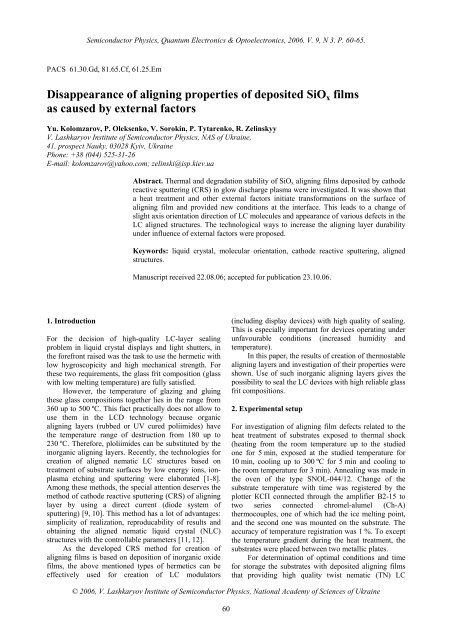
Semiconductor Physics, Quantum Electronics & Optoelectronics, 2006. V. 9, N 3. P. 60-65.<br />
PACS 61.30.Gd, 81.65.Cf, 61.25.Em<br />
<strong>Disappearance</strong> <strong>of</strong> <strong>aligning</strong> <strong>properties</strong> <strong>of</strong> <strong>deposited</strong> <strong>SiOx</strong> <strong>films</strong><br />
<strong>as</strong> caused by external factors<br />
Yu. Kolomzarov, P. Oleksenko, V. Sorokin, P. Tytarenko, R. Zelinskyy<br />
V. L<strong>as</strong>hkaryov Institute <strong>of</strong> Semiconductor Physics, NAS <strong>of</strong> Ukraine,<br />
41, prospect Nauky, 03028 Kyiv, Ukraine<br />
Phone: +38 (044) 525-31-26<br />
E-mail: kolomzarov@yahoo.com; zelinski@isp.kiev.ua<br />
1. Introduction<br />
Abstract. Thermal and degradation stability <strong>of</strong> <strong>SiOx</strong> <strong>aligning</strong> <strong>films</strong> <strong>deposited</strong> by cathode<br />
reactive sputtering (CRS) in glow discharge pl<strong>as</strong>ma were investigated. It w<strong>as</strong> shown that<br />
a heat treatment and other external factors initiate transformations on the surface <strong>of</strong><br />
<strong>aligning</strong> film and provided new conditions at the interface. This leads to a change <strong>of</strong><br />
slight axis orientation direction <strong>of</strong> LC molecules and appearance <strong>of</strong> various defects in the<br />
LC aligned structures. The technological ways to incre<strong>as</strong>e the <strong>aligning</strong> layer durability<br />
under influence <strong>of</strong> external factors were proposed.<br />
Keywords: liquid crystal, molecular orientation, cathode reactive sputtering, aligned<br />
structures.<br />
Manuscript received 22.08.06; accepted for publication 23.10.06.<br />
For the decision <strong>of</strong> high-quality LC-layer sealing<br />
problem in liquid crystal displays and light shutters, in<br />
the forefront raised w<strong>as</strong> the t<strong>as</strong>k to use the hermetic with<br />
low hygroscopicity and high mechanical strength. For<br />
these two requirements, the gl<strong>as</strong>s frit composition (gl<strong>as</strong>s<br />
with low melting temperature) are fully satisfied.<br />
However, the temperature <strong>of</strong> glazing and gluing<br />
these gl<strong>as</strong>s compositions together lies in the range from<br />
360 up to 500 ºC. This fact practically does not allow to<br />
use them in the LCD technology because organic<br />
<strong>aligning</strong> layers (rubbed or UV cured poliimides) have<br />
the temperature range <strong>of</strong> destruction from 180 up to<br />
230 ºC. Therefore, ploliimides can be substituted by the<br />
inorganic <strong>aligning</strong> layers. Recently, the technologies for<br />
creation <strong>of</strong> aligned nematic LC structures b<strong>as</strong>ed on<br />
treatment <strong>of</strong> substrate surfaces by low energy ions, ionpl<strong>as</strong>ma<br />
etching and sputtering were elaborated [1-8].<br />
Among these methods, the special attention deserves the<br />
method <strong>of</strong> cathode reactive sputtering (CRS) <strong>of</strong> <strong>aligning</strong><br />
layer by using a direct current (diode system <strong>of</strong><br />
sputtering) [9, 10]. This method h<strong>as</strong> a lot <strong>of</strong> advantages:<br />
simplicity <strong>of</strong> realization, reproducability <strong>of</strong> results and<br />
obtaining the aligned nematic liquid crystal (NLC)<br />
structures with the controllable parameters [11, 12].<br />
As the developed CRS method for creation <strong>of</strong><br />
<strong>aligning</strong> <strong>films</strong> is b<strong>as</strong>ed on deposition <strong>of</strong> inorganic oxide<br />
<strong>films</strong>, the above mentioned types <strong>of</strong> hermetics can be<br />
effectively used for creation <strong>of</strong> LC modulators<br />
© 2006, V. L<strong>as</strong>hkaryov Institute <strong>of</strong> Semiconductor Physics, National Academy <strong>of</strong> Sciences <strong>of</strong> Ukraine<br />
60<br />
(including display devices) with high quality <strong>of</strong> sealing.<br />
This is especially important for devices operating under<br />
unfavourable conditions (incre<strong>as</strong>ed humidity and<br />
temperature).<br />
In this paper, the results <strong>of</strong> creation <strong>of</strong> thermostable<br />
<strong>aligning</strong> layers and investigation <strong>of</strong> their <strong>properties</strong> were<br />
shown. Use <strong>of</strong> such inorganic <strong>aligning</strong> layers gives the<br />
possibility to seal the LC devices with high reliable gl<strong>as</strong>s<br />
frit compositions.<br />
2. Experimental setup<br />
For investigation <strong>of</strong> <strong>aligning</strong> film defects related to the<br />
heat treatment <strong>of</strong> substrates exposed to thermal shock<br />
(heating from the room temperature up to the studied<br />
one for 5 min, exposed at the studied temperature for<br />
10 min, cooling up to 300 ºC for 5 min and cooling to<br />
the room temperature for 3 min). Annealing w<strong>as</strong> made in<br />
the oven <strong>of</strong> the type SNOL-044/12. Change <strong>of</strong> the<br />
substrate temperature with time w<strong>as</strong> registered by the<br />
plotter КСП connected through the amplifier В2-15 to<br />
two series connected chromel-alumel (Ch-A)<br />
thermocouples, one <strong>of</strong> which had the ice melting point,<br />
and the second one w<strong>as</strong> mounted on the substrate. The<br />
accuracy <strong>of</strong> temperature registration w<strong>as</strong> 1 %. To except<br />
the temperature gradient during the heat treatment, the<br />
substrates were placed between two metallic plates.<br />
For determination <strong>of</strong> optimal conditions and time<br />
for storage the substrates with <strong>deposited</strong> <strong>aligning</strong> <strong>films</strong><br />
that providing high quality twist nematic (TN) LC
Semiconductor Physics, Quantum Electronics & Optoelectronics, 2006. V. 9, N 3. P. 60-65.<br />
structure were divided into three parts. First part w<strong>as</strong><br />
stored in a closed volume (drying bottle with silica gel),<br />
the second one w<strong>as</strong> stored under the room conditions<br />
(temperature w<strong>as</strong> 20…25 ºC and humidity 50…70 %),<br />
and third one – at the room temperature in a closed<br />
volume with saturated water vapor (distilled water).<br />
After that, every day one substrate from these three parts<br />
w<strong>as</strong> <strong>as</strong>sembled with the <strong>as</strong>-prepared test substrate and<br />
filled with NLC. After <strong>aligning</strong>, the obtained NLC structures<br />
were investigated using a polarization microscope.<br />
The images <strong>of</strong> the typical defects <strong>of</strong> TN LC structures<br />
were recorded. The quality <strong>of</strong> TN LC structures obtained<br />
by two test <strong>of</strong> the <strong>as</strong>-prepared and <strong>as</strong>sembled substrates<br />
w<strong>as</strong> high, and defects or imperfections were absent.<br />
To study the defects after thermal treatment <strong>of</strong> <strong>SiOx</strong><br />
<strong>aligning</strong> layers, four types <strong>of</strong> substrates were used. The<br />
first type w<strong>as</strong> made <strong>of</strong> K8 gl<strong>as</strong>s, the second one – silica,<br />
the third and fourth ones were made <strong>of</strong> gl<strong>as</strong>s and had the<br />
ITO electrodes (substrates for watch displays) opened<br />
and covered by SiO2, respectively. Deposition <strong>of</strong> <strong>SiOx</strong><br />
<strong>aligning</strong> layer w<strong>as</strong> carried out by the CRS method <strong>as</strong><br />
described in [10-13]. The parameters <strong>of</strong> the technological<br />
process were <strong>as</strong> follows: the applied cathode<br />
voltage U (from 2.5 up to 5 kV), current density J (from<br />
1 to 5 mA/cm 2 ), oxygen concentration kO (50 %). To<br />
study the preferable storage conditions <strong>of</strong> the prepared<br />
substrates with <strong>aligning</strong> layer, used were the substrates<br />
<strong>of</strong> the third and fourth types. The <strong>SiOx</strong> <strong>aligning</strong> layer<br />
w<strong>as</strong> on these substrates with the same parameters. In the<br />
course <strong>of</strong> deposition, three various values <strong>of</strong> oxygen<br />
concentrations kO (0, 50 or 100 %) were used.<br />
3. Results and discussion<br />
3.1. Defects <strong>of</strong> alignment after the heat treatment<br />
Our analysis showed that defects <strong>of</strong> alignment after the<br />
heat treatment differ and can be divided into four kinds<br />
according to the influence <strong>of</strong> the following factors:<br />
a) the heat treatment;<br />
b) substrate <strong>properties</strong>;<br />
c) evaporation <strong>of</strong> gl<strong>as</strong>s frit decomposition products;<br />
d) low temperature glue decomposition (tapes <strong>of</strong><br />
PVB, BF and others).<br />
a) b) c)<br />
Fig. 1. Defects <strong>of</strong> <strong>aligning</strong> at various annealing temperatures: 460 (a), 480 (b), and 500 ºC (c).<br />
© 2006, V. L<strong>as</strong>hkaryov Institute <strong>of</strong> Semiconductor Physics, National Academy <strong>of</strong> Sciences <strong>of</strong> Ukraine<br />
61<br />
At the annealing temperature in the range <strong>of</strong> 400 to<br />
520 ºC, <strong>aligning</strong> layers on silica, K8 gl<strong>as</strong>s and SiO2covered<br />
ITO electrodes (fourth type <strong>of</strong> substrates)<br />
created defectless high quality TN LC structures. It<br />
means that the <strong>SiOx</strong> <strong>aligning</strong> layer remains thermally<br />
stable up to 520 ºC for the enough wide ranges <strong>of</strong><br />
deposition technological parameters.<br />
Imperfect TN LC structures were obtained on the<br />
substrates <strong>of</strong> the third type (gl<strong>as</strong>s with opened ITO<br />
electrodes) when the annealing temperature w<strong>as</strong> higher<br />
than 450 ºC. These structures had a lot <strong>of</strong> defects such <strong>as</strong><br />
disclination lines surrounded by the squares <strong>of</strong> 0.1 to<br />
1 mm 2 located on the substrate surface in the area free <strong>of</strong><br />
ITO electrodes. The photos <strong>of</strong> these defects are shown in<br />
Fig. 1.<br />
However, the TN LC structures between ITO<br />
electrodes w<strong>as</strong> perfect after annealing <strong>of</strong> the substrates<br />
up to the temperature 515 ºC.<br />
The re<strong>as</strong>on <strong>of</strong> defect appearance on gl<strong>as</strong>s surface is<br />
the processes <strong>of</strong> gl<strong>as</strong>s lixiviation causing chemical<br />
interaction (for example, free sodium) with the <strong>deposited</strong><br />
<strong>SiOx</strong> film or mechanical destruction <strong>of</strong> <strong>aligning</strong> layer<br />
under the action <strong>of</strong> high annealing temperature. As w<strong>as</strong><br />
experimentally shown, the temperature <strong>of</strong> such defect<br />
appearance is in the range from 440 to 480 ºC and even<br />
sometimes up to 500 ºC and depending on the type <strong>of</strong><br />
gl<strong>as</strong>s substrates.<br />
As shown in Fig. 2, with incre<strong>as</strong>ing the cathode<br />
voltage the temperature <strong>of</strong> defect appearance w<strong>as</strong><br />
incre<strong>as</strong>ing, too. The re<strong>as</strong>on <strong>of</strong> such behavior is the<br />
higher temperature <strong>of</strong> ion treatment <strong>of</strong> substrate in the<br />
deposition process because <strong>of</strong> the greater ion energy.<br />
3.2. Defects related to the influence <strong>of</strong> gl<strong>as</strong>s frit<br />
Defects caused by the influence <strong>of</strong> evaporation <strong>of</strong> gl<strong>as</strong>s<br />
frit decomposition product on <strong>aligning</strong> layers at heat<br />
treatment have a sufficient difference in comparison<br />
with the considered above. In this c<strong>as</strong>e, the destruction<br />
<strong>of</strong> <strong>aligning</strong> layers w<strong>as</strong> observed on the surface <strong>of</strong> ITO<br />
electrodes. The photo <strong>of</strong> these defects is shown in Fig. 3.<br />
It w<strong>as</strong> noticed that defects appeared, when the annealing<br />
temperature w<strong>as</strong> by 20 to 40 ºC higher than that <strong>of</strong> gl<strong>as</strong>s
Semiconductor Physics, Quantum Electronics & Optoelectronics, 2006. V. 9, N 3. P. 60-65.<br />
frit melting. In Fig. 4 shown w<strong>as</strong> the experimental<br />
dependences <strong>of</strong> maximal annealing temperature<br />
providing the absence <strong>of</strong> defects on the temperature <strong>of</strong><br />
gl<strong>as</strong>s frit melting (for three types <strong>of</strong> gl<strong>as</strong>s frit with the<br />
values <strong>of</strong> melting temperature 380, 400 and 437 ºC).<br />
The analysis <strong>of</strong> ITO electrode defect appearance<br />
re<strong>as</strong>ons allows to <strong>as</strong>sume that destruction <strong>of</strong> alignment<br />
layer on ITO electrodes is the result <strong>of</strong> chemical<br />
interaction <strong>of</strong> fusible components <strong>of</strong> gl<strong>as</strong>s frit (for<br />
Fig. 2. Dependence <strong>of</strong> maximal temperature <strong>of</strong> substrate<br />
annealing (defectless orientation <strong>of</strong> TNLC) on the cathode<br />
voltage during SiO x <strong>aligning</strong> layer deposition.<br />
Fig. 3. Appearance <strong>of</strong> defects <strong>of</strong> the SiO2 <strong>aligning</strong> layer<br />
covering the ITO electrodes by frit gl<strong>as</strong>s vapor (480 ºC<br />
gluing) action.<br />
Fig. 4. Experimental dependences <strong>of</strong> maximal annealing<br />
temperature providing the absence <strong>of</strong> defects on the<br />
temperature <strong>of</strong> gl<strong>as</strong>s frit melting.<br />
© 2006, V. L<strong>as</strong>hkaryov Institute <strong>of</strong> Semiconductor Physics, National Academy <strong>of</strong> Sciences <strong>of</strong> Ukraine<br />
62<br />
example, compounds <strong>of</strong> lead) directly with the<br />
transparent conducting film that h<strong>as</strong> general formula<br />
In2O3:Sn, followed with a complete destruction <strong>of</strong><br />
<strong>aligning</strong> layer. The TN LC structure quality in the area<br />
free <strong>of</strong> ITO electrodes remains high.<br />
For the substrates <strong>of</strong> fourth type (made <strong>of</strong> gl<strong>as</strong>s and<br />
having the ITO electrodes covered with SiO2), these<br />
defects did not appear up to 520 ºC annealing<br />
temperature. It is natural to <strong>as</strong>sume that for excluding the<br />
defect appearance, it is necessary to provide the<br />
precision temperature control during gluing the<br />
substrates together with gl<strong>as</strong>s frit sealing. Thus, the<br />
incre<strong>as</strong>e <strong>of</strong> the gluing together temperature to<br />
500…515 ºC must be provided in the c<strong>as</strong>e when it is<br />
theoretically and practically grounded.<br />
3.3. Defects related to low temperature glues<br />
Defects <strong>of</strong> such type are mainly localized on a surface<br />
free <strong>of</strong> ITO electrodes and look similar to defects <strong>of</strong><br />
gl<strong>as</strong>s lixiviation, but they are more closely packed.<br />
Defects similar to these appeared over all the area<br />
covered by SiO2. Appearance <strong>of</strong> defects is caused by<br />
sedimentation <strong>of</strong> PVB and BF glues decomposition<br />
products on a surface <strong>of</strong> gl<strong>as</strong>s free <strong>of</strong> ITO electrodes or<br />
covered with SiO2. It should be noted that the examined<br />
defects appeared when superheating the glue or<br />
incre<strong>as</strong>ing the gluing time (at T = 80…100 ºC for 45 to<br />
60 min).<br />
Photos <strong>of</strong> typical defects caused by low<br />
temperature glue decomposition products on the <strong>aligning</strong><br />
layers are shown in Fig. 5.<br />
3.4. Influence <strong>of</strong> ionic treatment on a gl<strong>as</strong>s frit<br />
and ITO electrodes<br />
Using the <strong>SiOx</strong> <strong>aligning</strong> layer demands to take into<br />
account the influence <strong>of</strong> an ionic treatment on the<br />
<strong>properties</strong> <strong>of</strong> gl<strong>as</strong>s frit. High temperatures <strong>of</strong> substrate<br />
surface in the process <strong>of</strong> <strong>SiOx</strong> <strong>aligning</strong> layer deposition<br />
in a combination with ionic bombardment can result in<br />
destruction <strong>of</strong> gl<strong>as</strong>s frit partially or completely.<br />
Dependences <strong>of</strong> substrate surface temperature on<br />
technological parameters (cathode voltage, discharge<br />
power, concentrations <strong>of</strong> oxygen and argon, deposition<br />
Fig. 5. Typical defects caused by the influence <strong>of</strong> low<br />
temperature glue PVB and BF decomposition products on<br />
the <strong>aligning</strong> layer.
Semiconductor Physics, Quantum Electronics & Optoelectronics, 2006. V. 9, N 3. P. 60-65.<br />
angle) <strong>of</strong> <strong>SiOx</strong> <strong>aligning</strong> layer deposition were<br />
investigated. Some <strong>of</strong> these dependences are shown in<br />
Figs 6-8. The analysis <strong>of</strong> the dependences in Figs 6 to 8<br />
allows to draw the following conclusions.<br />
The substrate surface temperature in the course <strong>of</strong><br />
deposition <strong>of</strong> alignment layer strongly depends on the<br />
oxygen concentration, deposition angle and applied<br />
Fig. 6. Dependence <strong>of</strong> the substrate surface temperature during<br />
deposition on the cathode voltage for three various oxygen<br />
concentrations.<br />
Fig. 7. Dependence <strong>of</strong> the substrate surface temperature during<br />
deposition on the oxygen concentration for three various<br />
cathode voltages.<br />
Fig. 8. Dependence <strong>of</strong> the substrate surface temperature during<br />
deposition on the deposition angle for three various cathode<br />
voltages.<br />
© 2006, V. L<strong>as</strong>hkaryov Institute <strong>of</strong> Semiconductor Physics, National Academy <strong>of</strong> Sciences <strong>of</strong> Ukraine<br />
63<br />
cathode voltage. As were experimentally found, a gl<strong>as</strong>s<br />
frit during deposition becomes pl<strong>as</strong>tic at the temperature<br />
<strong>of</strong> 360 to 370 ºC and comparatively destroyed at the<br />
cathode voltages more than 4 kV. These circumstances<br />
put the following limitations on the deposition angle,<br />
cathode voltage and oxygen concentration: α ≤ 15º,<br />
U ≤ 4 kV, kO ≤ 50 %.<br />
To determine the optimal conditions and time for<br />
storage the substrates with <strong>deposited</strong> <strong>aligning</strong> <strong>films</strong> used<br />
w<strong>as</strong> the method described in Section 2.4.<br />
3.5. Influence <strong>of</strong> storage method on degradation<br />
<strong>of</strong> <strong>aligning</strong> layers<br />
After deposition <strong>of</strong> <strong>SiOx</strong> <strong>aligning</strong> layers at various<br />
oxygen concentrations, the substrates were stored in a<br />
closed volume (drying bottle with silica gel) for six days.<br />
After that they were <strong>as</strong>sembled and filled with NLC to<br />
create TN structures. The results <strong>of</strong> investigation <strong>of</strong> TN<br />
structures were shown in Fig. 9.<br />
The analysis <strong>of</strong> results showed that the degradation<br />
stability <strong>of</strong> <strong>aligning</strong> layers <strong>deposited</strong> in the atmosphere<br />
<strong>of</strong> oxygen 50 and 100 % is higher than in the atmosphere<br />
<strong>of</strong> pure argon. It is possibly caused by predominance in<br />
the <strong>SiOx</strong> alignment layer <strong>of</strong> lower silicon oxides, which<br />
much less shadow the surface <strong>of</strong> gl<strong>as</strong>s against moisture<br />
(the defects appear on gl<strong>as</strong>s mainly) and, at the same<br />
time, they very effective hydrate.<br />
a<br />
b<br />
c<br />
Fig. 9. Degradation <strong>of</strong> the SiO х <strong>aligning</strong> layer after six days <strong>of</strong><br />
storage in dry atmosphere, which w<strong>as</strong> <strong>deposited</strong> in: pure argon (a),<br />
mixture <strong>of</strong> 50 % oxygen and 50 % argon (b), pure oxygen (c).
Semiconductor Physics, Quantum Electronics & Optoelectronics, 2006. V. 9, N 3. P. 60-65.<br />
After storage <strong>of</strong> substrates in moist conditions the<br />
<strong>aligning</strong> <strong>properties</strong> <strong>of</strong> <strong>SiOx</strong> <strong>aligning</strong> layer <strong>deposited</strong> on<br />
gl<strong>as</strong>s are completely and very quickly destroyed (see<br />
Fig. 10).<br />
As the degradation <strong>of</strong> <strong>SiOx</strong> <strong>aligning</strong> layer is mainly<br />
determined by the presence <strong>of</strong> moisture, laboratory<br />
rooms in which the relative humidity from 40 to 80 %<br />
are useless for the long term storage <strong>of</strong> substrates after<br />
deposition. Nevertheless, at maintenance <strong>of</strong> some<br />
microclimate conditions <strong>of</strong> room (T = 20 ºC, humidity<br />
40 %) it is possible to guarantee the safe keeping <strong>of</strong><br />
<strong>deposited</strong> substrates for a few days. Fig. 11 represents<br />
a<br />
b<br />
Fig. 10. Degradation <strong>of</strong> the SiO x <strong>aligning</strong> layer <strong>deposited</strong><br />
on gl<strong>as</strong>s after storage in moist conditions for one (a) and<br />
two (b) days.<br />
a<br />
b<br />
Fig. 11. Degradation <strong>of</strong> the SiO x <strong>aligning</strong> layer after<br />
storage under room conditions for thirteen days: a) ITO<br />
electrodes covered by SiO 2, b) opened ITO electrodes.<br />
© 2006, V. L<strong>as</strong>hkaryov Institute <strong>of</strong> Semiconductor Physics, National Academy <strong>of</strong> Sciences <strong>of</strong> Ukraine<br />
64<br />
the TN LC structures, obtained between the substrates<br />
which were kept in the above laboratory conditions for<br />
thirteen days.<br />
4. Conclusions<br />
Thus, the results <strong>of</strong> researches allow to ground the<br />
choose <strong>of</strong> the following technological regimes for<br />
deposition <strong>of</strong> <strong>SiOx</strong> <strong>aligning</strong> layer for gl<strong>as</strong>s frit sealing:<br />
• cathode voltage is 4 kV (mainly, is limited to<br />
thermal stability <strong>of</strong> gl<strong>as</strong>s frit and possibilities <strong>of</strong> the<br />
high-voltage power supply <strong>of</strong> the industrial plants<br />
for CRS);<br />
• cathode current density is 5 mA/cm 2 (it is limited to<br />
the substrate heating temperature at the oxygen<br />
concentration 50 %);<br />
• oxygen concentration in the operating mixture <strong>of</strong><br />
g<strong>as</strong>es is 50 % (it is limited to the substrate heating<br />
temperature and requirements to the modern<br />
vacuum technological equipment);<br />
• deposition angle is 15º (it is determined by the<br />
requirement <strong>of</strong> high <strong>aligning</strong> <strong>properties</strong>, substrate<br />
heating temperature and rate <strong>of</strong> <strong>SiOx</strong> alignment<br />
layer deposition);<br />
• main factor determining the degradation <strong>of</strong> <strong>SiOx</strong><br />
<strong>aligning</strong> layers on storage is moisture. At the same<br />
time, to hydrogenate not <strong>SiOx</strong> alignment layer but<br />
surface <strong>of</strong> free gl<strong>as</strong>s;<br />
• <strong>SiOx</strong> <strong>aligning</strong> layer <strong>deposited</strong> on uncovered SiO2<br />
substrates can be storaged for 1-4 days under the<br />
room conditions, and they are able to demonstrate<br />
the perfect orientation, or 10 days in dry<br />
conditions;<br />
• <strong>SiOx</strong> <strong>aligning</strong> layer <strong>deposited</strong> onto uncovered SiO2<br />
substrates are considerably less exposed to the<br />
influence <strong>of</strong> moisture.<br />
References<br />
1. Z.M. Sun, J.M. Engels, I. Dozov, and G. Durand,<br />
Ar + beam sputtering on solid surfaces and nematic<br />
liquid crystal orientation // J. Phys. II France 4,<br />
p. 59-73 (1994).<br />
2. P. Chaudhari, J. Lacey, S.A. Lien, and J. Speidell,<br />
Atomic beam alignment <strong>of</strong> liquid crystal // Jpn J.<br />
Appl. Phys. 37(1-2), p. L55-L56 (1998).<br />
3. P. Chaudhari, J. Lacey, J. Doyle et al., Alignment<br />
<strong>of</strong> liquid crystal layers. United States Patent No<br />
6,061,114 (2000).<br />
4. P. Chaudhari, J. Lacey, J. Doyle, et al., Atomicbeam<br />
alignment <strong>of</strong> inorganic materials for liquidcrystal<br />
displays // Nature 411, p. 56-59 (2001).<br />
5. O. Yaroshchuk, R. Kravchuk, A. Dobrovolskyy,<br />
N. Klyui, and O. Korneta, LC alignment on the<br />
inorganic substrates treated with directed pl<strong>as</strong>ma<br />
flux // Proc. XI Intern. Symposium “Advanced<br />
Display Technologies”, Crimea, Ukraine, Sept. 8-<br />
12 (2002) p. 186-194.
Semiconductor Physics, Quantum Electronics & Optoelectronics, 2006. V. 9, N 3. P. 60-65.<br />
6. O. Yaroshchuk, R. Kravchuk, A. Dobrovolskyy,<br />
S. Pavlov, Pl<strong>as</strong>ma treatment <strong>as</strong> a method <strong>of</strong> inplane<br />
LC alignment // Proc. Eurodisplay’02,<br />
p. 421-424, 2002.<br />
7. P. Chaudhari, J. Lacey, J. Doyle et al., Method for<br />
forming alignment layer by ion beam surface<br />
modification // United States Patent No 6,665,033<br />
(2003).<br />
8. O. Yaroshchuk, R. Kravchuk, L. Dolgov, E. Telesh,<br />
A. Khokhlov, J. Brill, N. Fruehauf,<br />
M.A. Reijme, Liquid crystal alignment on the <strong>films</strong><br />
<strong>deposited</strong> by sputtering: dependence on target<br />
material and g<strong>as</strong>eous feed // Proc. XIV Intern.<br />
Symposium “Advanced Display Technologies”,<br />
Crimea, Ukraine, Oct. 10-14 (2005), p. 186-194.<br />
9. V. Sorokin, N. Kuzmin, P. Oleksenko, Yu. Kolomzarov,<br />
V. Semenist, R. Zelinskyy, Investigation<br />
<strong>of</strong> methods for molecular alignment in nematic and<br />
smectic liquid crystal displays // Mol. Cryst. Liquid<br />
Cryst. 215, p. 137-143 (1992).<br />
10. Yu. Kolomzarov, P. Oleksenko, V. Sorokin, P. Tytarenko,<br />
R. Zelinskyy, Oblique reactive cathode<br />
© 2006, V. L<strong>as</strong>hkaryov Institute <strong>of</strong> Semiconductor Physics, National Academy <strong>of</strong> Sciences <strong>of</strong> Ukraine<br />
65<br />
sputtering <strong>as</strong> a method for creation <strong>of</strong> orienting<br />
liquid crystal microrelief // Proc. XII Intern.<br />
Symposium “Advance Display Technology”,<br />
Korolyov, Moscow Region, Russia, August 25-28<br />
(2003), p. 150-153.<br />
11. Yu. Kolomzarov, P. Oleksenko, V. Sorokin, P. Tytarenko,<br />
R. Zelinskyy, Vacuum method for creation<br />
<strong>of</strong> liquid crystal orienting microrelief // Semiconductor<br />
Physics, Quantum Electronics and<br />
Optoelectronics 6(4), p. 528-532 (2003).<br />
12. Yu. Kolomzarov, P. Oleksenko, V. Sorokin, P. Tytarenko,<br />
R. Zelinskyy, Peculiar <strong>properties</strong> <strong>of</strong> LC<br />
orientation by thin inorganic oxide <strong>films</strong> obtained<br />
by glow discharge pl<strong>as</strong>ma / XV Conference on<br />
Liquid Crystals, edited by J. Zmija // Proc. SPIE<br />
5565 (Bellingham, WA, 2004) p. 359-364.<br />
13. Yu. Kolomzarov, P. Oleksenko, V. Sorokin, P. Tytarenko,<br />
R. Zelinskyy, Orienting <strong>properties</strong> <strong>of</strong> <strong>SiOx</strong><br />
<strong>films</strong> for high resolution LCD application // Proc.<br />
XIII Intern. SID Symposium ”Advance Display<br />
Technologies”, Raubichi, Belarus, Sept. 7-10<br />
(2004), p. 83-88.