PROBING THE ANDREEV DOUBLET
PROBING THE ANDREEV DOUBLET
PROBING THE ANDREEV DOUBLET

You also want an ePaper? Increase the reach of your titles
YUMPU automatically turns print PDFs into web optimized ePapers that Google loves.
tel-00772851, version 2 - 13 Jun 2013<br />
This thesis discusses two experiments highlighting the<br />
existence of a fermionic degree of freedom in the Josephson<br />
effect: the Andreev doublet. They are both performed on the most<br />
basic Josephson element, a one-atom contact between two superconducting<br />
electrodes.<br />
In the first one, we observed the disappearance of the supercurrent,<br />
which reflects the spontaneous trapping of a quasiparticle<br />
in one of two Andreev bound states.<br />
In the second experiment we achieved the photon-absorption<br />
spectroscopy of this two-level system, using a Josephson junction<br />
as an integrated on-chip microwave emitter and detector. The<br />
observed spectra are well accounted for by a spin-boson model<br />
including the Andreev doublet and an electromagnetic mode of the<br />
environment.<br />
Cette thèse décrit deux expériences mettant en lumière<br />
l'existence d'un dégré de liberté fermionique dans l'effet<br />
Josephson: le doublet d'Andreev. Elles sont toutes les deux<br />
réalisées sur l'élément Josephson le plus élémentaire qui soit, un<br />
contact atomique entre deux électrodes supraconductrices.<br />
Dans la première, nous avons observé la disparition du supercourant,<br />
qui traduit le piégeage spontané d'une quasiparticule<br />
dans l'un des deux états liés d'Andreev.<br />
Dans la seconde, nous avons réalisé la spectroscopie<br />
photonique de ce système à deux niveaux, en utilisant une jonction<br />
Josephson à la fois en tant qu'émetteur et détecteur microonde. On<br />
peut bien rendre compte des spectres observés avec un modèle<br />
spin-boson incluant le doublet d'Andreev et un mode électromagnétique<br />
de l'environnement.<br />
2013<br />
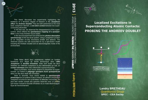
LOCALISED EXCITATIONS IN SUPERCONDUCTING<br />
ATOMIC CONTACTS: <strong>PROBING</strong> <strong>THE</strong> <strong>DOUBLET</strong><br />
Landry BRE<strong>THE</strong>AU<br />
Localized Excitations in<br />
Superconducting Atomic Contacts:<br />
<strong>PROBING</strong> <strong>THE</strong> <strong>ANDREEV</strong> <strong>DOUBLET</strong><br />
Landry BRE<strong>THE</strong>AU<br />
Quantronics Group<br />
SPEC - CEA Saclay
tel-00772851, version 2 - 13 Jun 2013<br />
LOCALIZED EXCITATIONS<br />
IN SUPERCONDUCTING ATOMIC CONTACTS:<br />
<strong>PROBING</strong> <strong>THE</strong> <strong>ANDREEV</strong> <strong>DOUBLET</strong><br />
Ph.D. dissertation<br />
by<br />
Landry BRE<strong>THE</strong>AU<br />
to obtain the degree of<br />
DOCTEUR de l’ECOLE POLYTECHNIQUE<br />
Ph.D. defense on February 1, 2013<br />
Committee in charge:<br />
Richard DEBLOCK<br />
Antoine GEORGES<br />
Leo KOUWENHOVEN<br />
Alberto MORPURGO (Rapporteur)<br />
Yuli NAZAROV (Rapporteur)<br />
Cristián URBINA<br />
Ph.D. Thesis directed by Hugues POTHIER and Cristián URBINA<br />
realized in the Quantronics Group<br />
Service de Physique de l’Etat Condensé, CEA-Saclay<br />
spec
tel-00772851, version 2 - 13 Jun 2013<br />
Cover<br />
Left picture: sketch of the energy spectrum of the Andreev bound states in the<br />
one-particle picture (see Part I, Fig. 2.8)<br />
Upper right picture: anomalous switching probability due to quasiparticle trapping<br />
(see Part II, Fig. 4.12)<br />
Lower right picture: measured excitation spectrum of the Andreev bound states<br />
(see Part III, Fig. 6.6)<br />
Localized excitations in superconducting atomic contacts: Probing the Andreev doublet<br />
Copyright © Février 2013 by Landry Bretheau<br />
Cover design by Landry Bretheau and Ioana Ocnarescu<br />
An electronic version of this dissertation is available at<br />
http://iramis.cea.fr/drecam/spec/Pres/Quantro/static/publications/phd-theses/<br />
http://hal.archives-ouvertes.fr/
tel-00772851, version 2 - 13 Jun 2013<br />
À mon Papa
tel-00772851, version 2 - 13 Jun 2013
tel-00772851, version 2 - 13 Jun 2013<br />
C’est à force d’observations, de réflexion, que l’on trouve.<br />
Ainsi, piochons, piochons continuellement.<br />
— Claude Monnet<br />
Il est idiot de monter une côte à bicyclette<br />
quand il suffit de se retourner pour la descendre.<br />
— Pierre Dac<br />
L’imagination est la plus scientifique des qualités.<br />
— Charles Baudelaire<br />
Quantum physics makes me so happy.<br />
It’s like looking at the universe naked.<br />
— Sheldon Cooper<br />
J’reprendrais bien un peu de purée !<br />
— Latex
tel-00772851, version 2 - 13 Jun 2013
tel-00772851, version 2 - 13 Jun 2013<br />
R E M E R C I E M E N T S<br />
Bien qu’en général loquace, l’écriture de ces remerciements m’est fort difficile.<br />
C’est assurément parce qu’ils signifient beaucoup tant j’ai de la gratitude et même<br />
souvent de l’amitié pour les personnes qui apparaissent dans ces quelques lignes.<br />
Je pourrais simplement les résumer à un MERCI suivi d’une liste de noms, un<br />
peu comme à la fin d’un film, mais cela resterait assez insipide. En réalité, il s’agit<br />
d’être sincère, et d’agrémenter ces mercis d’anecdotes personnelles, drôles, si possible<br />
sans tomber dans la caricature et tout en restant concis. Devant la difficulté<br />
de l’exercice, j’ai un temps pensé proposer une page de remerciements vierge ou<br />
le lecteur et heureux possesseur de cette thèse pourrait écrire ses propres remerciements<br />
à mon égard. Pris par un excès de modestie et comme je sais qu’il s’agit<br />
du chapitre qui sera le plus lu, je me lance.<br />
Les trois années (plus quelques mois) de thèse que j’ai passées au sein du groupe<br />
Quantronique ont été extrêmement intenses, d’un point de vue intellectuel, personnel<br />
et émotionnel.<br />
En premier lieu, je tiens à remercier mes deux directeurs de thèse préférés<br />
Hugues Pothier et Cristián Urbina. Merci de m’avoir supporté pendant ces trois<br />
ans de thèse, merci pour votre générosité, votre disponibilité et votre motivation<br />
au quotidien (et merci pour le temps très conséquent que vous avez consacré à la<br />
correction de ce manuscrit). Quelle belle école de découvrir la recherche avec vous !<br />
Chose assez extraordinaire, vous réussissez à allier rigueur, haut niveau, modestie,<br />
enthousiasme et autodérision. Cela se traduit par un travail d’équipe de qualité et<br />
dans la bonne humeur. On peut difficilement rêver mieux comme encadrants de<br />
thèse et comme collègues. Hugues, merci pour ton sens de l’humour sans pareil.<br />
J’adore ta vivacité d’esprit et ta faculté à conserver la moitié de ton cerveau à faire<br />
des blagues ou des vannes. Tu rends le quotidien plus léger. Cristián, merci pour<br />
ton humanité et ta sagesse. On a tellement discuté ensemble, et pas uniquement<br />
de physique. J’ai beaucoup appris et je te ressens un peu comme de ma famille.<br />
Daniel Estève, merci pour ton affection, ton caractère franc du collier, et pour<br />
tous les moments que tu as passé à m’expliquer la physique au tableau. Si le<br />
groupe Quantronique est une famille, tu y es pour beaucoup et tu y assumes très<br />
bien le rôle de père. Face aux bébés, tu es parfois même en mode papy gâteau,<br />
et j’adore comme tu harcèles les gens avec ton tact légendaire d’un petit “alors,<br />
c’est pour quand le bébé ? Il faut s’y mettre là !”. Je me souviens en particulier de<br />
ce formidable banquet chez toi, où on avait pu se délecter d’huitres format steak.<br />
Et le plaquage façon troisième ligne que tu avais mis à Andreas reste vraiment<br />
mémorable.<br />
Merci Pief Orfila pour ta disponibilité, ta bienveillance et ton grand sourire : tu<br />
rends la vie au labo plus simple. Et merci aussi pour ton sens de la dérision à<br />
l’égard de tous les gens du groupe.<br />
vii
tel-00772851, version 2 - 13 Jun 2013<br />
Marcelo Goffman, merci pour ton grand cœur et ta bonne humeur permanente.<br />
Même si c’était seulement pendant quelques mois, j’ai adoré travailler avec toi sur<br />
l’embryon de manip Majorana, et j’ai beaucoup appris. Et merci pour nous avoir<br />
donné accès à ta canne à 300 mK, et avoir gardé le sourire quand j’ai grillé les<br />
fils connectés aux batteries. Ton sourire justement et tes “che boludo” apportent le<br />
soleil dans le labo.<br />
Merci Denis Vion pour ta disponibilité et ta générosité en toutes circonstances.<br />
Que ce soit pour le MEB, Mathematica, Sonnet, tu as toujours été présent pour<br />
m’aider ... et aider l’ensemble de la communauté. En plus d’être un super physicien,<br />
tu es un peu une sorte d’homme-outil qui pousse la maîtrise de l’outil jusqu’à<br />
la compréhension de la logique de conception de l’outil même. Logique, après<br />
générosité, c’est un autre mot qui te caractérise. Tu es même le Torquemada de la<br />
logique et de l’intégrité ; c’est fascinant.<br />
Merci à Fabien Portier, mi-quantronicien, mi-nanoelectronicien et mi-molette (extravieille).<br />
Tu occupes une place bien à part pour moi. J’aime tellement parler<br />
physique, écouter de la zic, jouer à la coinche et manger des abats avec toi. Merci<br />
pour avoir participé à l’élaboration de ce pot dantesque. Et simplement, merci pour<br />
ta disponibilité, ta générosité et ton amitié.<br />
Merci à Pascal Senat pour la conception de la mécanique basse température et<br />
de la boîte de camembert du frigo. Et merci pour les discussions de tous les jours,<br />
les vannes et le très bon esprit lors des pots. Par contre, quelle faute de goût d’aller<br />
à la machine à café !<br />
Merci à Philippe Joyez pour le grand temps passé à parler notamment théorie<br />
P (E) et états d’Andreev, et le petit temps à tenter de Majoraniser ensemble. Face à<br />
ton manque de loquacité, j’ai toujours aimé te rentrer dans le lard pour te forcer à<br />
répondre à mes questions. Merci également pour les bières chez toi quand tu me<br />
détournais de mon entraînement de volley.<br />
Patrice Bertet, merci pour tout le temps que tu m’as donné à m’expliquer la<br />
physique. J’ai toujours adoré parler avec toi, car tu es d’une clarté rare. Merci aussi<br />
pour ton sens de l’humour quand je te charriais, notamment le fameux “Mais<br />
Patrice, tu ne connais pas le plaisir ...” de Cristián, que j’avais stoppé avant la fin<br />
de sa phrase (alors qu’on parlait de jouer au foot et marquer des buts).<br />
Merci à Thomas David, mon mentor en mécanique, toujours prêt à donner un<br />
coup de main et à discuter Itech, jeux videos et autres... Mention spéciale à ta<br />
journée des nouveaux arrivants en mode May the force be with you.<br />
Le groupe Quantronique, ce n’est pas que des vieux croutons, c’est aussi une<br />
armée de thésards et post-docs en pleine fleur de l’âge.<br />
En premier lieu, merci à mes deux post-docs, Maciej “baguette” Zgirski et Ça˘glar<br />
Girit (freestylise it !). Maciej, it was great facing the poisoning experiment together.<br />
Thanks for teaching me nanofabrication techniques, for the long talks at night and<br />
for your honesty about your thoughts, even the most conservative ones. Ça˘glar,<br />
ça a été tout simplement extraordinaire de travailler avec toi. Tu m’as tellement<br />
appris. Merci pour ta générosité, ta passion, ta confiance et ton soutien dans les<br />
moments difficiles. Je me souviens en particulier que tu m’avais confié (très tôt)<br />
que Claire était enceinte du futur Jin et ça m’avait beaucoup touché.<br />
viii
tel-00772851, version 2 - 13 Jun 2013<br />
Merci à Quentin Le Masne d’avoir eu la patience de me coacher lors de mes<br />
trois mois de stage précédant la thèse, et notamment de m’avoir fait découvrir<br />
les arcanes de la nano-fabrication. Merci à Andreas Dewes et Yuimaru Kubo, mes<br />
voisins de Bures-sur-Yvette, pour les soirées passés ensemble autour de bières allemandes<br />
et sakés japonais. Andreas, merci pour cette soirée magique après le pot de<br />
thèse de Simone ou tu as laissé JD conduire ta voiture. Yui, merci pour les supers<br />
cadeaux que tu m’as rapporté du Japon : gomu gomu no aligato ! Merci à Carles<br />
Altimiras, copain en devenir, pour ta passion contagieuse pour le foot, la physique,<br />
la bonne bière, et la bonne bouffe. Muchas gracias à Leandro Tosi pour m’avoir fait<br />
découvrir le maté : j’ai adoré le temps qu’on a passé ensemble, à maniper, discuter,<br />
jouer au foot et boire des bières ; c’était court mais intense.<br />
Merci également à François Mallet que j’apprends à découvrir maintenant, Charis<br />
Quay qui rigole si fort, Florian Ong qui me faisait rêver en tongs en salle blanche<br />
(j’ai été soft, j’ai pas fait de blague sur ong et tong), Agustin Palacios-Laloy pour<br />
le coaching sur Lyx, Max Hofheinz pour les discussions physiques qu’on a eu et<br />
le super accueil à Grenoble, Romain Lauro blagueur chuchoteur en séries, Vivien<br />
Schmitt mention spéciale bon esprit lors des pots (et ton stock de gnole dans ton bureau<br />
en cas de coup dur), Cécile Grezes qui n’oubliait pas de me charrier régulièrement,<br />
Olivier Parlavecchio et son goût si prononcé pour le jaune, Michael Stern et<br />
son “ça va bien ?” quotidien où on sent qu’il se soucie vraiment de comment ça<br />
va, et Xin Zhou toujours fraiche et souriante.<br />
Enfin, merci à Jean-Damien Pillet qui occupe une place bien à part ici étant<br />
donné qu’on est “super copains de la vie” depuis la primaire. C’était tout simplement<br />
génial de bosser dans le même groupe. Ça reste toujours un peu mystérieux<br />
pour moi qu’on se retrouve ensemble, après des chemins disjoints mais parallèles,<br />
et qui ne sont reliés qu’au moment de la thèse. La seule explication que je vois,<br />
c’est qu’on a tous deux excellent goût !<br />
Mais le SPEC ne se réduit pas au groupe Quantronique. Merci à nos plus proches<br />
voisins du groupe nanoélectronique. Christian Glattli, c’est toujours passionnant<br />
de parler physique avec toi (et merci pour Moriond!). Patrice “Iznogoud” Roche, ça<br />
change d’air d’avoir un physicien comme toi ; merci en particulier pour l’ensemble<br />
de tes blagues, et tout particulièrement pour celle des prêtres sous la douche qui<br />
reste la meilleure que j’ai entendu ces cinq dernières années. Preden Roulleau, c’est<br />
marrant comme nos routes se sont recroisées après ces randos sur glacier dix ans<br />
plus tôt à Aussois. Merci aussi à Iouri Moukharski, l’ours venu du froid (et prends<br />
bien soin de ma petite AX !).<br />
Merci aux nanomagnétiseurs, Olivier Klein, Michel Viret, Grégoire de Loubens,<br />
Claude Fermon, Myriam Pannetier-Lecœur et tous les jeunes pour nous avoir concurrencés<br />
sur la régularité des pots et des sessions gâteaux. Grâce à mon copain<br />
Benjamin Pigeau “marathonveganman” j’ai pu m’y incruster un bon nombre de<br />
fois ! Merci aussi à Olivier Rousseau pour tout le Kapton que tu nous as filé. Enfin<br />
merci aux membres des autres groupes qui participent à la vie du labo et que l’on<br />
peut croiser au détour de la salle café : entre autres Eric Varoquaux et Tito Williams,<br />
qui démontrent bien que la physique ça conserve, Alan Braslau, et mon fillot Ivan<br />
Dornic, docteur ès gravier. Merci à Jean-Marc Luck (dit Matthieu) de l’IPHT pour<br />
ix
tel-00772851, version 2 - 13 Jun 2013<br />
son aide sur mes petites questions de physique quantique. Merci également aux<br />
thésards des autres groupes qui ont participé à la bonne ambiance du labo, entre<br />
autres Rémy Lassalle-Balier (Mr macaron), Phuong-Anh Huynh, Julie Dubois, Andrei<br />
Mostovoi, Aurélie Solignac et Joël Acevedo (respo foot).<br />
Je tiens également à remercier les personnes qui font fonctionner le labo au<br />
quotidien. A la direction, Eric Vincent, François Daviaud et Patrice Roche. Au secrétariat,<br />
Nathalie Royer, Corinne Kopec-Coelho et Dijana Samson, les mamans du<br />
SPEC : Nathalie et Corinne, merci d’avoir eu la patience de m’expliquer une bonne<br />
dizaine de fois comment remplir un ordre de mission. A l’entretien, Nadine Le Bail<br />
avec qui j’ai pris plaisir à faire un petit brin de causette chaque jour. A l’atelier, Vincent<br />
Padilla, Dominique Duet, Jacques Prudowski, et Jean-Claude Tack : merci en<br />
particulier à Jean-Claude et Dominique pour la fabrication des pièces de la manip,<br />
et spéciale dédicace à Vincent pour ses conseils en harmonica et mobylette et pour<br />
sa folie grolandaise. J’y greffe Patrice Jacques qui m’a sauvé la mise en débouchant<br />
une bouteille d’hélium à coup de marteau. A la cryogénie, Philippe Forget, Mathieu<br />
de Combarieu et Patrick Pari : merci PP pour le rab d’hélium de ton doigt<br />
froid, pour la jolie manip de fontaine d’hélium superfluide avec le cryostat en<br />
verre, et pour si bien jouer ton personnage de PP ronchon. Au magasin, Pierre Janvier,<br />
toujours sympa et disponible et qui a toujours réussi à nous dégoter, même à<br />
la dernière minute, des bouteilles d’hélium. N’oublions pas le “maître de chantier”<br />
Jean-Michel Richomme et sa sonnerie Panthère Rose, la toujours souriante Nadine<br />
Genand-Riondet pour les subventions écoles, Claudine Chaleil responsable sécurité<br />
et salle blanche (avec Pief), et Roland Tourbot à la “bondeuse”. J’ai également<br />
une pensée spéciale pour certains membres du CEA qui nous facilitent le travail<br />
au quotidien : les fans du PSG, de moto et de Darth Vador au service des badges,<br />
le super responsable sécurité et son goût pour les photos de bébés carbonisés, et<br />
les membres de la FLS pour les parties de cache-cache dans la forêt.<br />
Pendant ma thèse, j’ai eu la chance de discuter avec de nombreux scientifiques<br />
qui m’ont permis d’améliorer ma compréhension de la physique. En premier lieu<br />
je remercie Manuel Houzet avec qui j’ai beaucoup échangé, ce qui s’est traduit par<br />
une collaboration sur la modélisation de notre manip (merci pour l’invitation à<br />
Grenoble !). Muchas gracias a los tres hispanohablantes Alfredo Levy Yeyati, Juan<br />
Carlos Cuevas y Sebastián Bergeret, por el recibimiento en Madrid y San Sebastián.<br />
Alfredo, te agradezco el haberme iniciado, junto a JD, al formalismo de Keldysh,<br />
y el haber sabido guardar silencio sobre nuestras correrías nocturnas por Madrid.<br />
Juan Carlos, gracias por habernos llevado de tapas por los mejores bares de Madrid.<br />
Sebastián, gracias por tu buen humor, tu pasión sin límites por la física y tu risa<br />
inimitable. Thanks to Hermann Grabert and Daniel Urban to show me the generalised<br />
Bogoliubov de Gennes formalism and to allow me to come to Capri. Special<br />
thanks to Vitaly Shumeiko and Yuli Nazarov for all you taught me about the Andreev<br />
bound states: thanks to you I understood the odd states ! And thanks Yuli<br />
for your “mauvaise foi” about P (E) theory: “I call ̷h banana and there is no longer<br />
anything quantum”. Merci à Michel Devoret pour son grand optimisme à chacune<br />
de ses visites : “des états impairs avec 100 µs de temps de vie, ça vous fait un ex-<br />
x
tel-00772851, version 2 - 13 Jun 2013<br />
cellent qubit !”. Thanks to Leonid Glazman for his questions about the odd states<br />
on the ski trails in the italian Alpes. Merci à Grégoire Ithier pour m’avoir fait visiter<br />
son labo pendant mon séjour à Windsor, à Eva Dupont-Ferrier pour son super<br />
accueil à Grenoble, and to Leo Kouwenhoven, Ronald Hanson and Leo Di Carlo<br />
for their warm welcome at Delft. Merci à Hélène Bouchiat pour les discussions<br />
dans les trains ou RER, à Silvano de Franceschi, sympa en toutes circonstances, au<br />
meethique Thierry Martin (j’ai un souvenir ému du plateau de fruits de mer “à<br />
la bonne franquette” en bord de mer) et au caustique Jérôme Cayssol (tu me dois<br />
toujours une bière). Merci aussi à Jean-Noël Fuchs, Hélène le Sueur, Tackis Kontos,<br />
Thibaut Jonckheere, Jacqueline Bloch, Julien Gabelli, Bertrand Reulet, Marco<br />
Aprili, Hervé Courtois et Francesco Giazotto.<br />
Je souhaite aussi remercier mes anciens professeurs avec qui j’ai continué à<br />
échanger. Merci Michel Héritier pour votre bienveillance sur mon avancée dans la<br />
science. Un grand merci à Benoît Douçot qui a toujours répondu à mes questions<br />
par email et n’a jamais rechigné à venir faire un tour à Saclay quand je le lui demandais.<br />
Je ne cesserai jamais d’être impressionné par ta profondeur en physique.<br />
Par contre, tu ne connais pas Lapinot ! Merci à Marc Gabay pour m’avoir pris<br />
comme chargé de TD (et merci KV Pham) et avoir répondu à mes questions existentielles<br />
sur les supras. Merci aussi à Pascal Simon pour les discussions Majorana,<br />
pour Aussois et la Sardaigne et pour les vannes.<br />
Une thèse c’est aussi l’opportunité au travers des conférences et des écoles de<br />
rencontrer d’autres jeunes apprenti-chercheurs de par le monde : Denis (I like),<br />
Alina, Mireia, Jörn and Pierre at Windsor, la team des grenoblois, Nico, Romain,<br />
Sergent, Whitehouse, Mathias à La Thuile, Anders and Alessandro at Capri, Natalia<br />
en Sardaigne, François et Mathias à Aussois. And Vincent, Daniel, Attila, Maja,<br />
Kun thanks for the warm welcome at Delft.<br />
I would like to thank very much the members of my thesis committee. First,<br />
thanks to the “rapporteurs” Alberto Morpurgo and Yuli Nazarov for taking the<br />
time to read the whole manuscript, and for writing such enthusiastic reviews. Special<br />
thanks to Yuli who made me king for a day on his blog with his kind words<br />
“The discussion with the opponent could have been more smooth, yet Landry managed<br />
to stay within the restrictions of formal politeness”. Richard Deblock, un<br />
grand merci pour ta lecture si attentive de mon manuscrit et l’ensemble des corrections<br />
que tu as fait l’effort de me transmettre. Leo Kouwenhoven, thanks for being<br />
part of my thesis committee, even if you could not be present the D-day. I’m glad<br />
that you are doing well now. Thanks for your interest and for your kind invitation<br />
to come to Delft. Enfin merci au président du jury, Antoine Georges, pour m’avoir<br />
fait découvrir “la physique des électrons dans les solides” et m’avoir conseillé, il<br />
y a de ça cinq ans, d’aller faire mon stage de M1 dans le groupe Quantronique.<br />
Je n’y étais pas allé, appelé par les sirènes parisiennes après deux ans passées<br />
sur le plateau de Palaiseau, mais j’avais bien gardé dans un coin de ma tête qu’il<br />
s’agissait d’une destination de choix.<br />
Je veux aussi remercier ma nouvelle équipe au LPA, le groupe Qélec : Benjamin<br />
Huard, François Mallet, Philippe Campagne-Ibarcq et Manu Flurin. Merci pour ce<br />
xi
tel-00772851, version 2 - 13 Jun 2013<br />
bel accueil et toutes les belles andouillettes à venir !<br />
Merci à tous mes copains, qui ont vécu de près ou de loin mes trois années de<br />
thèse : Olivier, Jd, Cécile, Lolo, Romain, Cristian, Pouille, Marion, Michou, Hélène,<br />
Lorenzo, Emma, Cyril, Hédi, Koju, Stan, Fabien, Benjamin, Flo, Pc, Otilia, Mihai<br />
et Roxana. Merci d’être mes amis et d’être là dans les moments heureux et difficiles.<br />
Merci de me charier et me remettre régulièrement en place. Et merci d’être<br />
venus en masse à ma soutenance. On a quand même descendu une vingtaine de<br />
bouteilles !<br />
Pour finir, je veux remercier ma famille pour leur amour et leur soutien sans<br />
borne. Merci à mon Papa, qui m’a fait tel que je suis et qui me manque tellement.<br />
Merci à ma Môman, qui m’a abreuvé et m’abreuve de son amour inconditionnel.<br />
Merci à ma meilleure grande soeur Lucile (virgule) que j’adore ; on sera toujours là<br />
l’un pour l’autre. Merci à mes grands-parents pour la merveilleuse usine à souvenir<br />
qu’ils m’ont offerte. Enfin, merci à ma Ioio, mon souffle, ma folie, mon picpalak<br />
pour la vie.<br />
Le groupe quantronique fin 2010.<br />
Devant, de gauche à droite : Ça˘glar Girit, Dijana Samson, Max Hofheinz, Patrice<br />
Bertet, Philippe Joyez, Denis Vion, Yuimaru Kubo, Landry Bretheau, Cristián<br />
Urbina, Thomas David. Derrière, de gauche à droite : Daniel Estève, Pief Orfila,<br />
Pascal Senat, Andreas Dewes, Hugues Pothier, Marcelo Goffman.<br />
xii
tel-00772851, version 2 - 13 Jun 2013<br />
C O N T E N T S<br />
1 introduction 1<br />
1.1 Andreev bound states in a nutshell . . . . . . . . . . . . . . . . . . . . 2<br />
1.2 Long-lived quasiparticles trapped in Andreev states . . . . . . . . . . 4<br />
1.3 Andreev states spectroscopy with a Josephson junction . . . . . . . . 7<br />
1.3.1 The Josephson junction spectrometer . . . . . . . . . . . . . . 7<br />
1.3.2 Detection of the excited Andreev state with the Josephson<br />
junction spectrometer . . . . . . . . . . . . . . . . . . . . . . . 8<br />
1.3.3 Quantum model . . . . . . . . . . . . . . . . . . . . . . . . . . 9<br />
1.4 Perspectives . . . . . . . . . . . . . . . . . . . . . . . . . . . . . . . . . 11<br />
I mesoscopic josephson effect and andreev bound states 13<br />
2 mesoscopic superconductivity and andreev bound states 15<br />
2.1 BCS Hamiltonian and Bogoliubov-de Gennes equation . . . . . . . . 15<br />
2.2 Homogeneous superconductor and representations . . . . . . . . . . 16<br />
2.2.1 Diagonalization of the Hamiltonian . . . . . . . . . . . . . . . 17<br />
2.2.2 Building the eigenstates: the one-particle picture . . . . . . . 17<br />
2.2.3 The excitation picture . . . . . . . . . . . . . . . . . . . . . . . 19<br />
2.2.4 The semiconductor picture . . . . . . . . . . . . . . . . . . . . 20<br />
2.2.5 Spectroscopy of superconductors . . . . . . . . . . . . . . . . . 22<br />
2.3 Normal-superconductor interface: the Andreev reflection . . . . . . . 24<br />
2.3.1 Energy dependence of the one-particle states . . . . . . . . . . 24<br />
2.3.2 Andreev reflection . . . . . . . . . . . . . . . . . . . . . . . . . 25<br />
2.4 Superconductor with both a phase gradient and a scattering potential 27<br />
2.4.1 Diagonalization of the Hamiltonian . . . . . . . . . . . . . . . 28<br />
2.4.2 The Andreev Bound States . . . . . . . . . . . . . . . . . . . . 28<br />
2.5 The Andreev two-level system . . . . . . . . . . . . . . . . . . . . . . 31<br />
2.5.1 The Andreev Hamiltonian . . . . . . . . . . . . . . . . . . . . . 31<br />
2.5.2 The Andreev current operator . . . . . . . . . . . . . . . . . . 32<br />
2.5.3 The Andreev inverse inductance operator . . . . . . . . . . . . 33<br />
2.5.4 Andreev Bound States as a spin- 1/2 in phase-dependent magnetic<br />
field . . . . . . . . . . . . . . . . . . . . . . . . . . . . . . 33<br />
2.5.5 Full quantization of the Andreev Hamiltonian . . . . . . . . . 34<br />
2.5.6 Extension to multiple channels . . . . . . . . . . . . . . . . . . 34<br />
2.6 The tunnel Josephson junction . . . . . . . . . . . . . . . . . . . . . . 35<br />
2.6.1 The Josephson Hamiltonian . . . . . . . . . . . . . . . . . . . . 35<br />
2.6.2 Currents through a Josephson junction . . . . . . . . . . . . . 35<br />
3 signatures of the abs and existing experimental evidence 37<br />
3.1 Current-phase relation . . . . . . . . . . . . . . . . . . . . . . . . . . . 37<br />
3.2 Flux modulation of the plasma frequency . . . . . . . . . . . . . . . . 40<br />
3.2.1 Classical inductance . . . . . . . . . . . . . . . . . . . . . . . . 40<br />
3.2.2 Quantum inductance . . . . . . . . . . . . . . . . . . . . . . . . 41<br />
3.3 Fractional Shapiro steps . . . . . . . . . . . . . . . . . . . . . . . . . . 42<br />
xiii
tel-00772851, version 2 - 13 Jun 2013<br />
xiv contents<br />
3.4 Multiple Andreev reflections . . . . . . . . . . . . . . . . . . . . . . . 43<br />
3.4.1 Dissipative MAR current . . . . . . . . . . . . . . . . . . . . . 43<br />
3.4.2 MAR shot noise . . . . . . . . . . . . . . . . . . . . . . . . . . . 48<br />
3.4.3 Photon-assisted MAR current . . . . . . . . . . . . . . . . . . . 50<br />
3.5 Quasiparticle-injection spectroscopy . . . . . . . . . . . . . . . . . . . 51<br />
II long-lived quasiparticles trapped in andreev bound states<br />
53<br />
4 poisoning measurements 55<br />
4.1 Experimental setup . . . . . . . . . . . . . . . . . . . . . . . . . . . . . 55<br />
4.1.1 Superconducting atomic contacts . . . . . . . . . . . . . . . . . 55<br />
4.1.2 The atomic-SQUID . . . . . . . . . . . . . . . . . . . . . . . . . 55<br />
4.1.3 A new design . . . . . . . . . . . . . . . . . . . . . . . . . . . . 57<br />
4.2 Principle of the measurements . . . . . . . . . . . . . . . . . . . . . . 59<br />
4.2.1 Characterization of the AC: I (V) measurement . . . . . . . . 59<br />
4.2.2 Switching current measurements . . . . . . . . . . . . . . . . . 59<br />
4.3 Evidence for poisoning . . . . . . . . . . . . . . . . . . . . . . . . . . . 64<br />
4.3.1 Correlation between switching events . . . . . . . . . . . . . . 64<br />
4.3.2 Stochastic suppression of the Andreev supercurrent . . . . . 66<br />
4.3.3 Poisoning and odd states . . . . . . . . . . . . . . . . . . . . . 68<br />
4.3.4 Multiple poisoning . . . . . . . . . . . . . . . . . . . . . . . . . 69<br />
4.4 Measurements of poisoning dynamics . . . . . . . . . . . . . . . . . . 69<br />
4.4.1 Exponential relaxation . . . . . . . . . . . . . . . . . . . . . . . 70<br />
4.4.2 Relaxation time and asymptotic probability as a function of<br />
the phase . . . . . . . . . . . . . . . . . . . . . . . . . . . . . . . 70<br />
4.4.3 Relaxation time and asymptotic probability as a function of<br />
the Andreev energy . . . . . . . . . . . . . . . . . . . . . . . . 74<br />
4.4.4 Origin of the boundaries of the anomalous phase region in<br />
Psw (ϕ, s) data . . . . . . . . . . . . . . . . . . . . . . . . . . . 75<br />
4.4.5 Origin of correlations in data without prepulses . . . . . . . . 76<br />
4.4.6 Initial poisoning . . . . . . . . . . . . . . . . . . . . . . . . . . 76<br />
4.5 Eliminating poisoning . . . . . . . . . . . . . . . . . . . . . . . . . . . 78<br />
5 modeling of the poisoning experiment 83<br />
5.1 Model for poisoning dynamics . . . . . . . . . . . . . . . . . . . . . . 83<br />
5.1.1 Master equation approach . . . . . . . . . . . . . . . . . . . . . 83<br />
5.1.2 Towards an interpretation of the energy threshold ? . . . . . . 86<br />
5.2 Why have we failed to detect the even excited state |+〉 ? . . . . . . . 87<br />
5.2.1 Relaxation due to photon emission . . . . . . . . . . . . . . . . 88<br />
5.2.2 Relaxation due to phonon emission . . . . . . . . . . . . . . . 89<br />
5.2.3 Discussion . . . . . . . . . . . . . . . . . . . . . . . . . . . . . . 90<br />
5.3 Conclusion . . . . . . . . . . . . . . . . . . . . . . . . . . . . . . . . . . 90<br />
5.4 Towards measuring the excited even state |+〉 . . . . . . . . . . . . . . 91<br />
III spectroscopy of andreev bound states with a josephson<br />
junction 93<br />
6 photon-absorption spectroscopy of the abs using a jjs 95<br />
6.1 Experimental setup . . . . . . . . . . . . . . . . . . . . . . . . . . . . . 95
tel-00772851, version 2 - 13 Jun 2013<br />
contents xv<br />
6.2 Experimental results . . . . . . . . . . . . . . . . . . . . . . . . . . . . 100<br />
6.2.1 Current-voltage characteristic of the Josephson junction spectrometer<br />
. . . . . . . . . . . . . . . . . . . . . . . . . . . . . . . 100<br />
6.2.2 Spectrum construction . . . . . . . . . . . . . . . . . . . . . . . 100<br />
6.2.3 Comparison of contacts . . . . . . . . . . . . . . . . . . . . . . 100<br />
6.3 Comparison with quantum model . . . . . . . . . . . . . . . . . . . . 103<br />
6.3.1 Andreev spin and plasma boson . . . . . . . . . . . . . . . . . 103<br />
6.3.2 Calculation of the spectra IJ (ϕ, VJ) . . . . . . . . . . . . . . . 105<br />
6.3.3 Amplitude of the resonances . . . . . . . . . . . . . . . . . . . 107<br />
6.3.4 Absorption and relaxation rates . . . . . . . . . . . . . . . . . 107<br />
6.4 Additional measurements . . . . . . . . . . . . . . . . . . . . . . . . . 108<br />
6.4.1 Big contact . . . . . . . . . . . . . . . . . . . . . . . . . . . . . . 108<br />
6.4.2 Library of spectra . . . . . . . . . . . . . . . . . . . . . . . . . . 109<br />
6.4.3 Out-of-equilibrium processes . . . . . . . . . . . . . . . . . . . 114<br />
6.5 Experiment on sample JS6 . . . . . . . . . . . . . . . . . . . . . . . . . 114<br />
6.6 Conclusions and perspectives . . . . . . . . . . . . . . . . . . . . . . . 116<br />
7 quantum theory for the spectroscopy of an atomic-squid<br />
by a jj 117<br />
7.1 Quantum description of electrical dipoles . . . . . . . . . . . . . . . . 117<br />
7.1.1 Josephson junction . . . . . . . . . . . . . . . . . . . . . . . . . 117<br />
7.1.2 Josephson channel . . . . . . . . . . . . . . . . . . . . . . . . . 118<br />
7.2 Quantum description of the electrical circuit . . . . . . . . . . . . . . 119<br />
7.2.1 Hamiltonian derivation . . . . . . . . . . . . . . . . . . . . . . 119<br />
7.2.2 Order of magnitudes of the parameters in our experiment . . 120<br />
7.3 Formal calculation of the Cooper pair current . . . . . . . . . . . . . 121<br />
7.3.1 Fermi’s golden rule . . . . . . . . . . . . . . . . . . . . . . . . . 121<br />
7.3.2 Comparison with the usual P(E) theory . . . . . . . . . . . . . 122<br />
7.4 Dealing with dissipation . . . . . . . . . . . . . . . . . . . . . . . . . . 122<br />
7.5 Solving the environment Hamiltonian . . . . . . . . . . . . . . . . . . 123<br />
7.5.1 First approximation . . . . . . . . . . . . . . . . . . . . . . . . 123<br />
7.5.2 The spin-boson model . . . . . . . . . . . . . . . . . . . . . . . 124<br />
7.5.3 Standard perturbation theory far from degeneracies . . . . . 126<br />
7.5.4 Jaynes-Cummings model close to degeneracy hνp = 2EA(ϕ) 129<br />
7.5.5 Beyond Jaynes-Cummings model: general perturbation theory 133<br />
7.5.6 Numerical resolution . . . . . . . . . . . . . . . . . . . . . . . . 134<br />
7.6 Extension to multiple channels . . . . . . . . . . . . . . . . . . . . . . 136<br />
7.6.1 Analytical resolutions . . . . . . . . . . . . . . . . . . . . . . . 136<br />
7.6.2 Numerical solution . . . . . . . . . . . . . . . . . . . . . . . . . 138<br />
7.7 IJ (ϕ, VJ) spectra . . . . . . . . . . . . . . . . . . . . . . . . . . . . . . 138<br />
7.8 Possible extensions . . . . . . . . . . . . . . . . . . . . . . . . . . . . . 138<br />
7.8.1 Modeling dissipation . . . . . . . . . . . . . . . . . . . . . . . . 138<br />
7.8.2 Beyond first order perturbation . . . . . . . . . . . . . . . . . . 138<br />
7.8.3 Out-of-equilibrium environment . . . . . . . . . . . . . . . . . 140<br />
8 switching spectroscopy of andreev bound states 141<br />
8.1 Current-phase relation measurement at equilibrium . . . . . . . . . . 141<br />
8.2 Switching spectroscopy . . . . . . . . . . . . . . . . . . . . . . . . . . . 142
tel-00772851, version 2 - 13 Jun 2013<br />
xvi contents<br />
8.2.1 Experimental protocol . . . . . . . . . . . . . . . . . . . . . . . 142<br />
8.2.2 Andreev transitions up to 2∆ . . . . . . . . . . . . . . . . . . . 144<br />
8.2.3 Transitions from the lower ABS to the continuum . . . . . . . 144<br />
8.2.4 Higher order processes . . . . . . . . . . . . . . . . . . . . . . 144<br />
8.2.5 Driving excitation during the bias measurement pulse . . . . 146<br />
8.2.6 Long-lived excited states ? . . . . . . . . . . . . . . . . . . . . . 146<br />
8.3 Sample and hold detector based on poisoning . . . . . . . . . . . . . 146<br />
8.3.1 Reduction of the atomic contact critical current . . . . . . . . 146<br />
8.3.2 Current-phase relation measurement in presence of microwaves147<br />
8.3.3 Odd states . . . . . . . . . . . . . . . . . . . . . . . . . . . . . . 148<br />
8.4 Comparison between spectra by absorption and by switching . . . . 149<br />
IV experimental techniques 151<br />
9 sample fabrication 153<br />
9.1 Sample PAL7 for switching experiment . . . . . . . . . . . . . . . . . 153<br />
9.1.1 Kapton wafer preparation . . . . . . . . . . . . . . . . . . . . . 153<br />
9.1.2 Optical lithography . . . . . . . . . . . . . . . . . . . . . . . . . 154<br />
9.1.3 Electron beam lithography . . . . . . . . . . . . . . . . . . . . 156<br />
9.2 Sample JT6 for spectroscopy experiment . . . . . . . . . . . . . . . . . 159<br />
9.2.1 Bronze wafer preparation . . . . . . . . . . . . . . . . . . . . . 159<br />
9.2.2 First electron beam lithography lithography . . . . . . . . . . 159<br />
9.2.3 Capacitor fabrication . . . . . . . . . . . . . . . . . . . . . . . . 159<br />
9.2.4 Second electron beam lithography lithography . . . . . . . . . 161<br />
9.2.5 Sample JS6 . . . . . . . . . . . . . . . . . . . . . . . . . . . . . . 164<br />
9.3 Nano-fabrication recipes . . . . . . . . . . . . . . . . . . . . . . . . . . 166<br />
9.3.1 Optical lithography . . . . . . . . . . . . . . . . . . . . . . . . . 166<br />
9.3.2 Electron-beam lithography . . . . . . . . . . . . . . . . . . . . 166<br />
9.3.3 Material deposition and lift-off . . . . . . . . . . . . . . . . . . 167<br />
9.3.4 Reactive ion etching . . . . . . . . . . . . . . . . . . . . . . . . 168<br />
10 low temperature measurements 169<br />
10.1 Sample Holder . . . . . . . . . . . . . . . . . . . . . . . . . . . . . . . 169<br />
10.2 Cryostat wiring . . . . . . . . . . . . . . . . . . . . . . . . . . . . . . . 171<br />
10.3 Room temperature connections and instruments . . . . . . . . . . . . 176<br />
10.3.1 Biasing . . . . . . . . . . . . . . . . . . . . . . . . . . . . . . . . 176<br />
10.3.2 Amplification . . . . . . . . . . . . . . . . . . . . . . . . . . . . 176<br />
10.3.3 Measurements . . . . . . . . . . . . . . . . . . . . . . . . . . . . 176<br />
V appendices 177<br />
a microscopic construction of the andreev bound states 179<br />
a.1 Normal state . . . . . . . . . . . . . . . . . . . . . . . . . . . . . . . . . 179<br />
a.1.1 Second quantization formalism . . . . . . . . . . . . . . . . . . 179<br />
a.1.2 Free electrons . . . . . . . . . . . . . . . . . . . . . . . . . . . . 180<br />
a.1.3 Repulsive scattering potential . . . . . . . . . . . . . . . . . . . 181<br />
a.2 Superconducting regime . . . . . . . . . . . . . . . . . . . . . . . . . . 184<br />
a.2.1 BCS Hamiltonian and Bogoliubov-de Gennes equation . . . . 184<br />
a.2.2 Homogeneous superconductor . . . . . . . . . . . . . . . . . . 185<br />
a.2.3 Normal-superconductor interface: the Andreev reflection . . 189
tel-00772851, version 2 - 13 Jun 2013<br />
contents xvii<br />
a.2.4 Construction of the Andreev Bound States . . . . . . . . . . . 190<br />
a.2.5 The Andreev two-level system . . . . . . . . . . . . . . . . . . 195<br />
b notes on the andreev two-level system 201<br />
b.1 First derivation (Ivanov and Feigelman) . . . . . . . . . . . . . . . . . 201<br />
b.2 Second derivation (Zazunov et al.) . . . . . . . . . . . . . . . . . . . . 201<br />
b.2.1 Phase-independent basis . . . . . . . . . . . . . . . . . . . . . . 201<br />
b.2.2 Current operator basis . . . . . . . . . . . . . . . . . . . . . . . 202<br />
b.2.3 Andreev states basis . . . . . . . . . . . . . . . . . . . . . . . . 202<br />
c hamiltonian description of an electromagnetic environment<br />
205<br />
c.1 Single-mode environment: the LC harmonic oscillator . . . . . . . . . 205<br />
c.1.1 Impedance calculation . . . . . . . . . . . . . . . . . . . . . . . 205<br />
c.1.2 Hamiltonian derivation in second quantization formalism . . 207<br />
c.2 Arbitrary impedance . . . . . . . . . . . . . . . . . . . . . . . . . . . . 207<br />
c.2.1 Impedance calculation: Caldeira-Leggett decomposition . . . 207<br />
c.2.2 Hamiltonian derivation in second quantization formalism . . 208<br />
d andreev bound states dynamics 209<br />
d.1 Semi-classical treatment . . . . . . . . . . . . . . . . . . . . . . . . . . 209<br />
d.1.1 Instantaneous two-level Hamiltonian . . . . . . . . . . . . . . 209<br />
d.1.2 Landau-Zener transition . . . . . . . . . . . . . . . . . . . . . . 210<br />
d.1.3 Rabi oscillations in presence of a classical microwave excitation211<br />
d.1.4 Berry phase of the Andreev bound states . . . . . . . . . . . . 212<br />
d.2 Quantum fluctuations of the phase . . . . . . . . . . . . . . . . . . . 213<br />
d.2.1 Full quantization of the Andreev Hamiltonian . . . . . . . . . 213<br />
d.2.2 Transition rates of an Andreev two-level system coupled to<br />
its electromagnetic environment . . . . . . . . . . . . . . . . . 214<br />
e supplementary materials on the switching experiment 217<br />
e.1 Characterization of PAL7 . . . . . . . . . . . . . . . . . . . . . . . . . 217<br />
e.2 Calculation of the switching probability . . . . . . . . . . . . . . . . . 218<br />
e.2.1 Escape theory for a single Josephson junction . . . . . . . . . 218<br />
e.2.2 Escape theory for an atomic-SQUID . . . . . . . . . . . . . . . 220<br />
f classical calculation of asymmetrical squids 223<br />
f.1 Two tunnel Josephson junctions in parallel . . . . . . . . . . . . . . . 223<br />
f.1.1 Critical current . . . . . . . . . . . . . . . . . . . . . . . . . . . 223<br />
f.1.2 Plasma frequency . . . . . . . . . . . . . . . . . . . . . . . . . . 224<br />
f.2 Tunnel JJ in parallel with a JC of transmission τ . . . . . . . . . . . . 225<br />
f.2.1 Critical current . . . . . . . . . . . . . . . . . . . . . . . . . . . 225<br />
f.2.2 Plasma frequency . . . . . . . . . . . . . . . . . . . . . . . . . . 226<br />
f.2.3 The tilted washboard potential . . . . . . . . . . . . . . . . . . 227<br />
g supplementary materials on spectroscopy experiments 229<br />
g.1 Equivalent circuit for sample JT6 . . . . . . . . . . . . . . . . . . . . . 229<br />
g.2 Determination of the transmissions of contacts U and V . . . . . . . 230<br />
g.3 Determination of the voltage VJ across the JJS . . . . . . . . . . . . . 230<br />
g.4 Subtraction procedure for the absorption spectroscopy . . . . . . . . 232<br />
g.5 Additional theoretical spectra . . . . . . . . . . . . . . . . . . . . . . . 232<br />
g.6 Switching spectrum for contact U . . . . . . . . . . . . . . . . . . . . . 235
tel-00772851, version 2 - 13 Jun 2013<br />
xviii contents<br />
h alternative method: solving the environment hamiltonian<br />
in the andreev charge basis 239<br />
h.1 Matrix representation of Henv . . . . . . . . . . . . . . . . . . . . . . . 239<br />
h.2 Symmetry and reduction of degeneracy . . . . . . . . . . . . . . . . . 240<br />
h.3 Numerical resolution . . . . . . . . . . . . . . . . . . . . . . . . . . . . 242<br />
i spectroscopy of the plasma mode of a symmetrical squid 245<br />
i.1 Experimental setup . . . . . . . . . . . . . . . . . . . . . . . . . . . . . 245<br />
i.2 Experimental results . . . . . . . . . . . . . . . . . . . . . . . . . . . . 246<br />
j ac je and dcb of a jj: classical calculation 249<br />
j.1 Motivations . . . . . . . . . . . . . . . . . . . . . . . . . . . . . . . . . 249<br />
j.2 Notations . . . . . . . . . . . . . . . . . . . . . . . . . . . . . . . . . . . 250<br />
j.3 Ohmic resistance as an environment: analytical resolution . . . . . . 251<br />
j.3.1 Notations . . . . . . . . . . . . . . . . . . . . . . . . . . . . . . 251<br />
j.3.2 r 1 . . . . . . . . . . . . . . . . . . . . . . . . . . . . . . . . . 251<br />
j.3.3 r < 1 . . . . . . . . . . . . . . . . . . . . . . . . . . . . . . . . . 252<br />
j.4 Arbitrary impedance Z(ω): perturbative resolution . . . . . . . . . . 256<br />
j.4.1 Notations . . . . . . . . . . . . . . . . . . . . . . . . . . . . . . 256<br />
j.4.2 Order 0 . . . . . . . . . . . . . . . . . . . . . . . . . . . . . . . . 258<br />
j.4.3 Order 1 . . . . . . . . . . . . . . . . . . . . . . . . . . . . . . . . 258<br />
j.4.4 Order 2 . . . . . . . . . . . . . . . . . . . . . . . . . . . . . . . . 260<br />
j.4.5 Order 3 . . . . . . . . . . . . . . . . . . . . . . . . . . . . . . . . 261<br />
j.4.6 Interpretation . . . . . . . . . . . . . . . . . . . . . . . . . . . . 262<br />
j.5 Discussion . . . . . . . . . . . . . . . . . . . . . . . . . . . . . . . . . . 263<br />
j.5.1 What comes from this calculation ? Harmonics: multi-Cooper<br />
pairs processes . . . . . . . . . . . . . . . . . . . . . . . . . . . 263<br />
j.5.2 What is quantum ? Sub-harmonics: multi-photons processes 264<br />
j.6 Numerical resolution . . . . . . . . . . . . . . . . . . . . . . . . . . . . 265<br />
j.6.1 Harmonic oscillator . . . . . . . . . . . . . . . . . . . . . . . . 265<br />
k ac je and dcb of a jc: classical calculation 269<br />
k.1 Hypothesis and notations . . . . . . . . . . . . . . . . . . . . . . . . . 269<br />
k.2 Ohmic resistance as an environment: analytical resolution . . . . . . 270<br />
k.2.1 Notations . . . . . . . . . . . . . . . . . . . . . . . . . . . . . . 270<br />
k.2.2 r 1 . . . . . . . . . . . . . . . . . . . . . . . . . . . . . . . . . 270<br />
k.2.3 r = 0 . . . . . . . . . . . . . . . . . . . . . . . . . . . . . . . . . 271<br />
k.2.4 r < 1 . . . . . . . . . . . . . . . . . . . . . . . . . . . . . . . . . 272<br />
k.3 Arbitrary impedance Z(ω): perturbative resolution . . . . . . . . . . 274<br />
k.3.1 Notations . . . . . . . . . . . . . . . . . . . . . . . . . . . . . . 274<br />
k.3.2 Order 0 . . . . . . . . . . . . . . . . . . . . . . . . . . . . . . . . 274<br />
k.3.3 Order 1 . . . . . . . . . . . . . . . . . . . . . . . . . . . . . . . . 275<br />
k.3.4 Perturbation in τ ≪ 1 . . . . . . . . . . . . . . . . . . . . . . . 275<br />
k.4 Conclusion . . . . . . . . . . . . . . . . . . . . . . . . . . . . . . . . . . 277<br />
l reflectometry measurements of an atomic-squid in a superconducting<br />
cavity 279<br />
l.1 Experimental setup . . . . . . . . . . . . . . . . . . . . . . . . . . . . . 279<br />
l.2 Experimental results . . . . . . . . . . . . . . . . . . . . . . . . . . . . 280<br />
l.3 Interpretation . . . . . . . . . . . . . . . . . . . . . . . . . . . . . . . . 284
tel-00772851, version 2 - 13 Jun 2013<br />
contents xix<br />
l.3.1 Level repulsion and avoided crossing . . . . . . . . . . . . . . 284<br />
l.3.2 Additional experiment on sample RAC3 . . . . . . . . . . . . 286<br />
l.3.3 Towards coherent manipulation of the ABS ? . . . . . . . . . . 287<br />
bibliography 289<br />
index 301
tel-00772851, version 2 - 13 Jun 2013<br />
A C R O N Y M S<br />
ABS Andreev bound states<br />
JC Josephson channel<br />
JJ Josephson junction<br />
AC Atomic contact<br />
MAR multiple Andreev reflections<br />
JJS Josephson junction spectrometer<br />
DCB dynamical Coulomb blockade<br />
xx
tel-00772851, version 2 - 13 Jun 2013<br />
I N T R O D U C T I O N<br />
A variety of circuits and devices have been developed based on the Josephson effect<br />
since its prediction and observation fifty years ago [1, 2, 3, 4, 5]. Currently, Josephson<br />
circuits that behave like artificial atoms [6] are revolutionizing the way we<br />
probe and exploit the laws of quantum physics. Experiments embedding these artificial<br />
atoms in microwave cavities can even surpass their atomic physics counterparts<br />
[7]. The crucial component in these circuits is the Josephson tunnel junction:<br />
two superconducting electrodes separated by a thin insulating barrier allowing<br />
weak tunneling of Cooper pairs. A Josephson junction (JJ) in a circuit acts as an anharmonic<br />
oscillator whose dynamics can be described in terms of a single bosonic<br />
degree of freedom: the superconducting phase difference across the junction. However,<br />
the Josephson effect is not only observed in tunnel junctions but also in other<br />
weak links such as point contacts, graphene, carbon nanotubes, semiconducting<br />
nanowires, and thin ferromagnetic layers [8]. The microscopic understanding of<br />
the Josephson effect applicable to all weak links is that discrete states called Andreev<br />
bound states [9, 10, 11], localized at the weak link, carry the supercurrent<br />
[12, 13, 14, 15]. Andreev states come in pairs in each conduction channel of the<br />
weak link, symmetric in energy about the Fermi level. A pair of states behaves<br />
like a spin- 1/2 and introduces a fermionic degree of freedom to the Josephson effect.<br />
My thesis explores this additional fermionic degree of freedom, ignored in<br />
Josephson circuits developed up to now.<br />
Is it possible to address and control “Andreev spins”? This thesis describes<br />
two experiments designed to answer this question using atomic contacts between<br />
superconducting electrodes. Superconducting atomic contacts are simple, ideal<br />
weak-links. They accommodate only a small number of channels, whose transmission<br />
can be varied and measured in situ [16, 17]. They allow quantitative comparison<br />
between theory and experiment, with no adjustable parameters. In our work,<br />
we have used nano-fabricated break junctions [18] to obtain atomic contacts. This<br />
allows for very stable contacts which can be integrated in on-chip circuits.<br />
Part I of this manuscript presents the main concepts of the mesoscopic Josephson<br />
effect and of Andreev bound states (ABS) in a personal view developed as I worked<br />
through the vast literature on the subject. It also presents experimental evidence<br />
for the existence of ABS prior to my thesis. Although much had been achieved in<br />
atomic contacts and in carbon nanotubes, the transition between the two ABS in a<br />
channel had never been directly observed. This was the main goal of my thesis<br />
work.<br />
While pursuing this goal we discovered that under some conditions a single<br />
quasiparticle can be trapped in the Andreev bound states of an atomic contact<br />
and stay there for remarkably long times. As we will see in Part II, this “poisoning”<br />
phenomenon illustrates the different types of microscopic excitations and the<br />
fermionic character of the ABS.<br />
1<br />
1
tel-00772851, version 2 - 13 Jun 2013<br />
2 introduction<br />
Using a JJ as an integrated on-chip microwave emitter and detector, we were able<br />
to perform the first photon-absorption spectroscopy of Andreev bound states.<br />
This experiment is described in Part III, which also contains the quantum theory I<br />
developed to explain the results. This result opens the way to coherent manipulation<br />
of this two level system, an Andreev qubit.<br />
Part IV presents the experimental techniques that were used during this work.<br />
Finally, several detailed calculations and additional experiments are presented<br />
in separate appendices (Part V).<br />
1.1 Andreev bound states in a nutshell<br />
Within the mesoscopic theory of the Josephson effect, the basic Josephson weak<br />
link is a single conduction channel of arbitrary transmission probability τ connecting<br />
two superconducting electrodes. For a channel shorter than the superconducting<br />
coherence length, the Josephson coupling between both sides is established by<br />
a single pair 1 of ABS [13, 14, 15]. As depicted in the left panel of Fig. 1.1, in the oneparticle<br />
picture of the superconducting state [19] the ABS lie at energies ±EAinside<br />
the superconducting gap [−∆, ∆]:<br />
E<br />
∆<br />
0<br />
−∆<br />
E A<br />
EA = ∆<br />
<br />
2∆ 1−τ<br />
π 2π<br />
-E A<br />
δ<br />
1 − τ sin 2<br />
δ<br />
E A<br />
-E A<br />
<br />
δ<br />
. (1.1)<br />
2<br />
Figure 1.1: Left: Energy spectra in the one-particle picture of the ABS as a function of the<br />
phase difference 1 δ between two superconducting electrodes through a single short channel 1<br />
τ = 0.95. Right: The four states obtained with various + occupation of the ABS. 1- 1-τ<br />
These 1-τ fermionic microscopic states are similar to Cooper pair states of the bulk<br />
superconductor 0 (see Chapter 2). The crucial , difference is that their condensation 0<br />
energy E/ ∆ −EA can be smaller in absolute value than the energy gap ∆ and depends I /<br />
on the phase difference δ. Contrary to states in the continuum, they are spatially<br />
localized inside the weak link when their energy is deep inside the gap. The right<br />
-<br />
panel of -1 Fig. 1.1 shows the four global states resulting from the possible fermionic -1<br />
π 2π 0<br />
π 2π<br />
0<br />
1 A new pair of ABS is likely to appear each time the length exceeds a multiple of the superconducting<br />
coherence length.<br />
R b<br />
V<br />
V<br />
I<br />
∆<br />
0<br />
−∆<br />
∆<br />
E A<br />
0<br />
-E A<br />
−∆<br />
{τ } i<br />
ϕ<br />
I0 δ γ<br />
-<br />
I (µA)<br />
δ<br />
1<br />
0.5<br />
0<br />
-0.5<br />
∆<br />
E A<br />
0<br />
-E A<br />
−∆<br />
∆<br />
E A<br />
0<br />
-E A<br />
−∆<br />
+<br />
e∆<br />
h<br />
supercurrent<br />
T 1 (µs<br />
p ∞<br />
ϕ / π
tel-00772851, version 2 - 13 Jun 2013<br />
1.1 andreev bound states in a nutshell 3<br />
occupations of the ABS. There are two even states: the ground state |−〉 and the<br />
excited state |+〉 with energies −EA and +EA, respectively. There are also two odd<br />
excited states [20] with zero energy, denoted by |↑〉 and |↓〉, obtained by adding or<br />
subtracting a single quasiparticle from the system in the ground state. The even<br />
and odd denomination comes from the number of electrons participating in these<br />
localized states. The two odd states are generally ignored in the literature because<br />
parity conservation is implicitly assumed.<br />
Because phase is the quantum conjugate variable to the number of Cooper pairs<br />
that have gone through the channel, the phase dependence of the Josephson coupling<br />
energy leads to a supercurrent. In the ground state it is given by:<br />
IA = 1 ∂ (−EA)<br />
=<br />
ϕ0 ∂δ<br />
∆ τ sin (δ)<br />
<br />
4ϕ0 1 − τ sin 2 E<br />
- +<br />
∆<br />
∆<br />
∆<br />
E E A<br />
A<br />
E 0<br />
0<br />
A<br />
-E -E A<br />
A<br />
−∆<br />
−∆<br />
2∆ 1−τ<br />
0<br />
δ<br />
π 2π<br />
<br />
(1.2)<br />
-E ∆<br />
∆<br />
A<br />
δ<br />
−∆<br />
where ϕ0 = ̷h/2e is the reduced flux quantum. -E The energies -E A<br />
Aand<br />
supercurrents of<br />
−∆<br />
−∆<br />
the four states |−〉, |+〉, |↑〉 and |↓〉 are represented in Fig. 1.2. The two even states<br />
E/ ∆<br />
1<br />
1-τ<br />
0<br />
-1<br />
0<br />
I<br />
I<br />
π 2π<br />
δ<br />
C<br />
L<br />
+<br />
,<br />
-<br />
E A<br />
ϕ<br />
δ γ<br />
0<br />
0<br />
δ<br />
E A<br />
2<br />
0<br />
-1<br />
π 2π<br />
1<br />
1- 1-τ<br />
Figure 1.2: Energies (left) and supercurrents (right) of the four different configurations of<br />
the ABS versus the phase difference for a superconducting short 1 single channel of trans-<br />
supercurrent<br />
mission τ = 0.95. Whereas the even states |−〉 and |+〉 carry opposite supercurrent, the<br />
odd R ones |↑〉 and |↓〉 do{τ not } i carry any. I0 0.5<br />
b<br />
ϕ<br />
δ γ<br />
|−〉 and |+〉 carry opposite supercurrents +IA and I (µA) −IA, 0 and are those usually<br />
V<br />
called the ABS. The two odd states |↑〉 and |↓〉 have zero energy, and therefore carry<br />
-0.5<br />
no supercurrent Vb -1<br />
2 . Hence, the phase dependence of the supercurrent reveals the<br />
occupation configuration of the Andreev system.<br />
At zero temperature, only the negative-energy states are filled-400 in the one-particle 0<br />
picture. The Josephson coupling energy is simply −EA, and the supercurrent V (µV) IA<br />
-600 -200 200<br />
is only3 carried by the ABS of negative energy. It is remarkable that a single micro-<br />
scopic state determines the flow of a macroscopic current in a many-body system.<br />
In prior work on ABS in the Quantronics group, the supercurrent-phase relation,<br />
i.e. the dc Josephson effect, has been measured and compared quantitatively with<br />
predictions Rb [21]. At finite voltage, fractional Shapiro steps resulting from the non-<br />
p<br />
harmonicity of the current-phase relation have been observed [22]. They fit well<br />
E A(δ)<br />
2 This is valid in a spin degenerate system. However, in presence of spin-orbit interaction, the odd<br />
V<br />
states can b also carry supercurrent [20].<br />
{τ } I 3 This is valid only in the short junction i limit, where phase 0dependence<br />
of continuum states is negligible<br />
[14]. Then, the Josephson supercurrent is only transported by the Andreev States.<br />
0<br />
I /<br />
e∆<br />
h<br />
T 1 (µs)<br />
400<br />
p ∞<br />
ϕ / π<br />
∆<br />
100<br />
600<br />
10<br />
1<br />
0.2<br />
0.1<br />
0<br />
2<br />
1<br />
0<br />
0 0.25
tel-00772851, version 2 - 13 Jun 2013<br />
4 introduction<br />
to the predictions of the mesoscopic theory for the ac Josephson effect. These two<br />
experiments probed successfully the ground state |−〉. On the other hand, measurements<br />
of the dissipative current at finite voltage [16], its associated shot noise<br />
[23], and photon assisted current [22] have been quantitatively explained in terms<br />
of Multiple Andreev Reflections (multiple Andreev reflections (MAR)). Although<br />
this MAR phenomenon relies on the Andreev internal degree of freedom, i.e. on the<br />
existence of the excited even state |+〉, the latter has never been directly observed.<br />
Apart from atomic contacts, ABS physics has been explored in other systems,<br />
such as superconductor normal superconductor (SNS) junctions [24, 25, 26, 27]. But<br />
the direct observation of discrete ABS has been achieved only recently by tunneling<br />
spectroscopy of a carbon nanotube connected to two superconducting aluminum<br />
electrodes [28]. This experiment is a quasiparticle addition spectroscopy in which<br />
transitions between the ground state |−〉 and the odd states |↑〉 and |↓〉 are probed.<br />
It is complementary to the experiments presented here and does not address the<br />
even excited state |+〉.<br />
1.2 Long-lived quasiparticles trapped in Andreev states<br />
Both theory and experiment indicate that the number of quasiparticles in superconductors<br />
decreases exponentially as the temperature is lowered, while their recombination<br />
time increases [29, 30]. However at temperatures much lower than the<br />
transition temperature, it is difficult to reach an equilibrium Fermi-Dirac distribution.<br />
For example, Martinis et al. [31] measured that in a JJ Qubit, at temperatures<br />
below 70 mK, the number of quasiparticles saturates. These non-equilibrium quasiparticles<br />
are detrimental and set a limit to the proper functioning of superconducting<br />
devices such as microwave resonators [32] and Josephson qubits [33, 34].<br />
More drastically, a single quasiparticle can determine the response of single<br />
Cooper pair devices [35, 36], which contain small superconducting islands in which<br />
the parity of the total number of electrons matters. The trapping of a single quasiparticle<br />
in such a superconducting island has been dubbed poisoning [37], as it<br />
inhibits the behavior expected of the ground state of the system. Remarkably, it<br />
has been argued [20] that quasiparticle trapping could also occur in ABS in a constriction<br />
between two superconductors, a system containing no island at all. This<br />
trapping should induce an excitation from the even ground state |−〉, to either one<br />
of the odd excited states |↓〉 or |↑〉, which in turn should manifest itself as a change<br />
of supercurrent. To reach these odd states one has to change the local parity of<br />
the system. This is exactly what happens in a tunneling spectroscopy experiment<br />
where electrons are injected from an auxiliary electrode [28]. This is also what<br />
happened spontaneously in our experiment [38].<br />
The principle of the experiment is sketched in Fig. 1.3 (a). An Atomic contact (AC)<br />
in parallel with a JJ forms what we call an “atomic-SQUID”. The current-voltage<br />
characteristic of a specific atomic-SQUID measured at 30 mK, with a distinct supercurrent<br />
branch, is shown in Fig. 1.3 (b). The Josephson supercurrent through the<br />
atomic-SQUID is modulated by the applied flux. Because of the large asymmetry<br />
between the AC and the JJ (critical current of the JJ I0 550nA much larger than<br />
the typical critical current of a one-atom aluminum contact ∼ 50nA), the modula
2∆ 1−τ<br />
tel-00772851, version 2 - 13 Jun 2013<br />
L<br />
2π<br />
2π<br />
-E -E 1<br />
A<br />
A<br />
0<br />
(a)<br />
2<br />
−∆<br />
−∆<br />
1<br />
1 1<br />
δ<br />
+<br />
1- 1-τ ϕ / π 1<br />
1.2 long-lived quasiparticles trapped 0.2 in andreev states 5<br />
∆<br />
1-τ<br />
∆<br />
(c)<br />
{0.994, 0.1<br />
E 0<br />
E 0<br />
,<br />
{0.96, 0.03<br />
A<br />
A<br />
0<br />
e∆<br />
0 0.25 0.50<br />
tionE/ corresponds ∆0<br />
essentially 0 to the current-phase relation p of the atomic I / contact. In<br />
{0.91, 0.62<br />
0.1 h<br />
∞<br />
practice -E what is actually-E {0.85,<br />
measured is the “switching current” of the SQUID, i.e. the<br />
EA / ∆0.22<br />
A<br />
A<br />
(b)<br />
current −∆<br />
-1for<br />
which the system −∆ jumps -<br />
{0.74, 0.01<br />
from the zero-voltage state -1 (or supercurrent<br />
0<br />
π 2π 0<br />
π 0 2π<br />
branch) to the dissipative branch.<br />
2<br />
δ<br />
δ<br />
1<br />
+<br />
I<br />
1- 1-τ<br />
1<br />
R b<br />
V b<br />
(a)<br />
sc<br />
NS V<br />
ϕ<br />
δ γ<br />
E<br />
{τ i }<br />
ω J<br />
ϕ<br />
,<br />
-<br />
0<br />
eVJ I0 {τ } i I0 ϕ<br />
0<br />
δ γ<br />
e∆ I (µA)<br />
I /<br />
h<br />
V b<br />
r<br />
1<br />
0.5<br />
0<br />
-0.5<br />
V J<br />
-1<br />
-600<br />
-400<br />
ω J<br />
I<br />
J<br />
-200<br />
0<br />
V (µV)<br />
Σ<br />
supercurrent<br />
200<br />
400<br />
600<br />
ϕ<br />
δ γ<br />
∆<br />
We attribute this effect to the trapping of a spurious 40 quasiparticle from the delocalized<br />
continuum states into the 20<br />
=2E ABS of this channel. This is sketched in Fig. 1.4,<br />
A<br />
drawn in 0the<br />
excitation picture where the<br />
π 2π δ two I ABS0are degenerate<br />
J<br />
4 . This trapping<br />
−∆<br />
(b)<br />
2eV=hω J<br />
∆<br />
0<br />
r<br />
E<br />
J<br />
E<br />
-1<br />
π 2π<br />
δ<br />
2e<br />
E<br />
ω J<br />
E A(δ)<br />
∆<br />
hω J<br />
ω J<br />
I<br />
J<br />
Σ<br />
(b)<br />
p<br />
(nA)<br />
60<br />
-20<br />
-40<br />
ϕ / π<br />
∆<br />
(c)<br />
0<br />
0 0.25 0.50 0.75<br />
-60<br />
-400 -200 0 200 400<br />
ϕ<br />
(µV)<br />
V J<br />
E A / ∆<br />
Figure 1.3: Left: I SchematicLsetup: an atomic contact (magenta triangles) forms an atomic-<br />
SQUID with a Josephson junction (green checked box). Reduced flux threading the loop<br />
ϕ is imposed by a superconducting coil. Phases δ and γ across contact and junction are<br />
1<br />
linked R as δ − γ = ϕ. The SQUID is connectedsupercurrent through superconducting lines. It is biased<br />
b<br />
ϕ<br />
by a voltage source Vb I in series with a resistance Rb. The current I is measured p from the<br />
voltage 0 drop across Rb. C0.5<br />
Right: δ Current-voltage characteristics γ<br />
of an atomic-SQUID∆ with<br />
contact V transmissions {0.95, 0.45, 0.10}. The supercurrent of the EA(δ) SQUID, indicated with an<br />
b<br />
arrow, is modulated I (µA) by<br />
0<br />
the{τ applied } flux. The Ifinite subgap current is mainly due to MAR<br />
γ<br />
i 0<br />
processes.<br />
-0.5<br />
150<br />
This technique has been used to measure accurately the supercurrent as a func-<br />
-1<br />
tion of phase in the ground state |−〉 [21]. However, for a series of samples we<br />
-400 0 400<br />
observed discrepancies from the expected behavior [38]. For highly transmitting<br />
V (µV)<br />
contacts the supercurrent is strongly reduced within a broad phase interval around<br />
-600 -200 200 600<br />
V 100<br />
π. This reduction corresponds exactly to the full suppression of the Andreev su- J<br />
percurrent of the most transmitted channel.<br />
sc<br />
N I<br />
0<br />
S<br />
J0 {τ } I<br />
Figure 1.4: Excitation −∆ spectrum: besides the usual continuum of states above i the energyL0<br />
gap which extends all across −∆ the structure there is a discrete Andreev spin degenerate<br />
doublet localized at the constriction. The doublet has energy EA (δ) above the ground<br />
state and can trap quasiparticles with a probability p. The degeneracy has been lifted here<br />
for clarity. (c) (d)<br />
E<br />
4 The different representations are discussed in Chapter 2.<br />
50<br />
0<br />
V b<br />
0<br />
(a)<br />
r<br />
V J<br />
150<br />
V 100<br />
J<br />
50<br />
0<br />
V b<br />
0<br />
(a)<br />
N<br />
ω J<br />
L<br />
π<br />
ϕ<br />
I<br />
I J0
tel-00772851, version 2 - 13 Jun 2013<br />
δ<br />
∆<br />
E A<br />
0<br />
-E A<br />
−∆<br />
∆<br />
E A<br />
0<br />
-E A<br />
−∆<br />
+<br />
-1<br />
π 2π<br />
0.5<br />
)<br />
1<br />
0<br />
-0.5<br />
-1<br />
-600<br />
-400<br />
-200<br />
6 introduction<br />
1<br />
1- 1-τ<br />
0<br />
I /<br />
0<br />
corresponds to an excitation from the even ground state |−〉, to either one of the<br />
odd excited states |↓〉 or |↑〉, which carry no supercurrent.<br />
Quasiparticle trapping is stochastic and described by a probability p. We have<br />
measured the dynamics of this nonequilibrium phenomenon as a function of the<br />
phase for different atomic contacts. The corresponding relaxation time T1 and<br />
asymptotic poisoning probability p∞ are shown in Fig. 1.5 as a function of Andreev<br />
energy of the most transmitted channel. Trapping is more efficient when<br />
the ABS are deep inside the superconducting gap, i.e. for phase around π and for<br />
high transmission, in which case the lifetime of trapped quasiparticles is found to<br />
exceed 100 µs. Moreover, the trapping depends on Andreev energy in a non-trivial<br />
way: it occurs essentially when the Andreev energy is smaller than half the superconducting<br />
gap. The origin of this sharp energy threshold is not quite understood,<br />
but could be related to processes involving the emission of photons of the plasma<br />
mode of the SQUID.<br />
e∆<br />
h<br />
V (µV)<br />
supercurrent<br />
200<br />
T 1 (µs)<br />
400<br />
p ∞<br />
ϕ / π<br />
100<br />
600<br />
10<br />
1<br />
0.2 {0.994, 0.10, 0.10}<br />
{0.96, 0.03, 0.03}<br />
0.1<br />
0<br />
2<br />
(b)<br />
{0.91, 0.62, 0.15}<br />
{0.85, 0.22, 0.22}<br />
{0.74, 0.01}<br />
1<br />
(a)<br />
(c)<br />
0<br />
0 0.25 0.50 0.75 1.00<br />
E A / ∆<br />
Figure 1.5: Relaxation data for five different atomic contacts [transmissions are given in<br />
panel (b)] as a function of Andreev energy of the most transmitted channel: (a) relaxation<br />
time T1, (b) asymptotic poisoning probability p∞. There is a sharp threshold at EA <br />
0.5 ∆ for all contacts. For each contact, the energy of the most transmitting channel varies<br />
between √ 1 − τ ∆ and ∆, as shown in (c).<br />
Let us mention that poisoning can be avoided altogether. If the large scale onchip<br />
wires connecting the SQUID are made of either a normal metal L or a superconductor<br />
with a lower gap than the device, they act as good quasiparticle traps<br />
and poisoning is not observed. In contrast, the samples described here had a fully<br />
superconducting environment. This was to optimize the lifetime of the even ex-<br />
V J<br />
150<br />
100
tel-00772851, version 2 - 13 Jun 2013<br />
1.3 andreev states spectroscopy with a josephson junction 7<br />
cited state |+〉 in order to allow for its detection in switching experiments.The idea<br />
was to shine microwaves through an on-chip coplanar antenna which couples to<br />
the flux threading the SQUID loop and to detect a change in supercurrent. We did<br />
not succeed in driving this transition, probably because the life-time of the excited<br />
state was still too short.<br />
1.3 Andreev states spectroscopy with a Josephson junction<br />
We then changed drastically the scheme to excite and detect transitions. Instead of<br />
measuring a change in the ABS current induced by an excitation, we measured the<br />
microwave power absorption by the ABS. This method has the advantage of not<br />
requiring a long-lived excited state. To perform this spectroscopy we used an onchip<br />
voltage biased Josephson junction both as an emitter and a detector. Having<br />
an on-chip emitter allows a high-frequency, broadband coupling which greatly<br />
facilitates the experiments.<br />
1.3.1 The Josephson junction spectrometer<br />
When a JJ is voltage-biased below the superconducting gap VJ < 2∆/e, there is a<br />
vanishingly small dc quasiparticle current 5 and an ac Cooper pair current at the<br />
Josephson frequency<br />
νJ = VJ<br />
. (1.3)<br />
2πϕ0<br />
Therefore, from the electrical point of view, a voltage-biased JJ acts as an on-chip<br />
ac current generator. This current flows through the environment of the junction<br />
where it can excite electromagnetic modes. If this happens, a finite dc current IJ<br />
flows through the junction. From the microscopic point of view (see Fig. 1.6), it<br />
can be interpreted as arising from inelastic tunneling of Cooper pairs through the<br />
insulating barrier: the energy 2eVJ released by a Cooper pair is absorbed in the<br />
environment as a photon6 of energy hνJ. Thus, each mode of the environment of<br />
the JJ should appear as a dc current peak in its sub-gap current-voltage IJ(VJ) characteristic.<br />
The peak position gives the mode frequency, and its amplitude the rate<br />
at which the mode absorbs photons. Consequently, a voltage-biased JJ behaves as<br />
an on-chip broadband spectrometer7 : we call it the Josephson junction spectrometer<br />
(JJS).<br />
This physics, directly related to dynamical Coulomb blockade in superconducting<br />
systems [39, 40, 41], is an active research subject, with experiments involving<br />
superconducting resonators as perfectly controlled environments [42, 43]. Spectrometers<br />
based on Josephson junctions are also used to characterize microwave<br />
properties of materials [44, 45] or mesoscopic circuits [46, 47, 48, 49]. Here, we<br />
have chosen to use Josephson spectroscopy to explore the Andreev physics.<br />
5 This is true for a tunnel junction where MAR processes are negligible.<br />
6 This is valid for first order processes where one Cooper pair emits one photon.<br />
7 The highest frequency is obtained when VJ = 2∆/e. For bulk aluminum, it is ∼ 170 GHz.
)<br />
200<br />
tel-00772851, version 2 - 13 Jun 2013<br />
400<br />
I L0<br />
γ<br />
8 introduction<br />
N<br />
eV J<br />
i<br />
JJS atomic-SQUID V J (µV)<br />
∆<br />
0<br />
−∆<br />
E<br />
2e<br />
E<br />
∆<br />
0<br />
−∆<br />
N<br />
L0<br />
-60<br />
-400 -200 0 200 400<br />
hν J<br />
2eV J =<br />
=2E A (δ)<br />
∆<br />
0<br />
−∆<br />
E<br />
hν J<br />
E A<br />
-E A<br />
π 2π<br />
Figure 1.6: Principle of Andreev spectroscopy: (left) BCS density of states in the two electrodes<br />
of the JJS, shifted by the bias energy eVJ. A Cooper pair tunneling through the<br />
insulating barrier releases energy 2eVJ as a photon of frequency νJ, which is absorbed in<br />
the atomic-contact by exciting the Andreev transition (right).<br />
1.3.2 Detection of the excited Andreev state with the Josephson junction spectrometer<br />
As sketched in Fig. 1.6, the idea is to drive the Andreev transition by matching the<br />
Josephson frequency of the spectrometer to its energy: hνJ = 2EA (δ, τ). In practice<br />
(see Fig. 1.7 (a)), a JJS (critical current IJ0 50 nA) is capacitively coupled through<br />
an on-chip capacitance Σ to an atomic-SQUID (critical current IL0 1 µA). Fig. 1.7<br />
(b) shows an example of the spectrometer IJ(VJ) characteristic for a particular<br />
atomic contact. In addition to a large peak near 45 µV, several smaller peaks are<br />
observed, which vary in position with the applied flux ϕ 8 .<br />
The two left-most panels of Fig. 1.8 display the current IJ through the spectrometer<br />
junction as a function of both the phase δ across the atomic contact and the bias<br />
voltage VJ, for two different atomic contacts. Some resonances depend strongly on<br />
flux and are very different from one contact to the other. We identify them as the<br />
Andreev resonances in the channels of the contacts. As shown by the dotted lines<br />
in the right-half of each panel, they are quite well accounted for by the Andreev<br />
transition energies 2EA (δ, τi), calculated using Eq. 1.1 with the corresponding sets<br />
of transmissions {τi}, independently measured from the I (V) of each SQUID 9 . The<br />
Andreev lines become increasingly faint at high energy.<br />
There are some additional lines in the spectra shown in Fig. 1.8 which do not<br />
correspond to Andreev transitions. Among them, two very large resonances, at<br />
VJ 45 µV and 90 µV, cross Andreev resonances and slightly vary with flux. They<br />
correspond to the plasma mode of the SQUID and its first harmonic, i.e. to transitions<br />
between the levels of the oscillator formed by the Josephson inductance of<br />
the SQUID and the total capacitance C in parallel with it. One can also see other<br />
lines, corresponding neither to an Andreev nor to a plasma resonance, which are<br />
explained below.<br />
8 The peaks which depend neither on flux nor on the contact realization are related to resonances in<br />
the external environment and can be safely subtracted from all measured IVs.<br />
9 In reality, the atomic-SQUID is also connected to a separate voltage source through additional lines<br />
not represented in Fig. 1.7 (a).<br />
δ
0<br />
tel-00772851, version 2 - 13 Jun 2013<br />
γ<br />
R b<br />
(a)<br />
V b<br />
V J<br />
I J0<br />
ϕ<br />
1.3 andreev states spectroscopy with a josephson junction 9<br />
ν J<br />
I<br />
J<br />
2e<br />
Σ<br />
ϕ<br />
δ γ<br />
{τ i }<br />
JJS atomic-SQUID<br />
I L0<br />
(b)<br />
10<br />
0 120 20<br />
0 IJ 0.1<br />
-20<br />
-40<br />
70 120<br />
-60<br />
-400 -200 0 200 400<br />
V J (µV)<br />
60<br />
40<br />
(nA)<br />
Figure 1.7: (a) Simplified schematic of the setup: a voltage-biased Josephson junction (yellow<br />
checked box) acts as a microwave source and detector. It is coupled through capacitor<br />
Σ to an atomic-SQUID. The ac Josephson current excites electromagnetic modes of the<br />
E<br />
atomic-SQUID and Andreev transitions in the contact. The E magnetic flux ϕ threading the<br />
E<br />
loop imposes the phase δ across the contact and determines the Andreev transition fre-<br />
∆<br />
quency of each channel. These photonic excitations are∆detected as sub-gap current peaks<br />
in the current-voltage characteristics ∆<br />
of the 2eVjunction. = (b) Example EA of a current-voltage<br />
J<br />
IJ(VJ) 0<br />
N<br />
characteristic of the JJS . The large peak=2E in the (δ) upper inset corresponds to the plasma<br />
A<br />
mode of the eVatomic-SQUID. 2e The IJ(VJ) characteristic is0 shown for two<br />
J<br />
π different 2π flux δval<br />
ues at higher magnification 0 (lower inset). N The small flux-dependent peaks correspond to<br />
Andreev transitions. −∆<br />
-EA −∆<br />
−∆<br />
1.3.3 Quantum model<br />
To describe the full spectra we have developed a quantum model to treat the JJS<br />
coupled to its environment. In this model, tunneling of Cooper pairs through the<br />
JJS is treated as a perturbation. The current is obtained by a Fermi golden rule<br />
using eigenstates and eigenenergies of the environment alone 10 .<br />
The environment of the JJS is restricted to the atomic-SQUID. Its Hamiltonian<br />
hν J<br />
hν J<br />
HSQUID = HA(δ) + ̷hωp(a + a + 1<br />
) (1.4)<br />
2<br />
contains two terms. The first one describes the AC. In the two-level system approximation<br />
11 , the Andreev Hamiltonian [50] of a Josephson channel 12 is<br />
HA(δ) = −EA (δ) σ z(δ)<br />
(1.5)<br />
where σz is the Pauli matrix. The physics of the ABS is analogous to that of a spin-<br />
1/2 in a magnetic field whose amplitude EA and direction depend both on the<br />
phase δ. The second term describes the JJ of the SQUID, which is treated simply as<br />
a harmonic oscillator 13 of frequency ωp/2π, the plasma frequency. The destruction<br />
10 This modeling is analogous to the well-known P(E) theory for Dynamical Coulomb Blockade [39, 40],<br />
except that the environment, which includes the Andreev doublet, is highly non-linear and cannot<br />
be described by an impedance.<br />
11 This is valid only when neglecting the continuum and assuming that parity is conserved, thus restricting<br />
to the subspace {|−〉 , |+〉}.<br />
12 For multiple channels contacts, the Hamiltonian is just the sum <br />
HA,τi of the Hamiltonian of each<br />
channel.<br />
13 It corresponds to a first order Taylor expansion of the Josephson Hamiltonian.<br />
i
tel-00772851, version 2 - 13 Jun 2013<br />
10 introduction<br />
ν J (GHz)<br />
ν J (GHz)<br />
80<br />
60<br />
40<br />
20<br />
0<br />
80<br />
60<br />
40<br />
20<br />
0<br />
Contact V<br />
Contact U<br />
0 π<br />
ϕ<br />
2π<br />
(nA)<br />
I J<br />
1<br />
0.1<br />
0.01<br />
Theory for contact V<br />
Theory for contact U<br />
0 π<br />
ϕ<br />
2∆<br />
3∆<br />
2<br />
∆<br />
∆<br />
2<br />
0<br />
2∆<br />
3∆<br />
2<br />
∆<br />
∆<br />
2<br />
0<br />
2π<br />
2eV J<br />
2eV J<br />
Figure 1.8: Experimental (left) and calculated (right) spectra IJ (VJ, ϕ) for contact V<br />
({0.987, 0.37, 0.12} (top) and U {0.942, 0.26, 0.081} (bottom). The blind regions (gray) are<br />
not accessible to measurement with this setup. The log current scale is the same for<br />
the two spectra. Dotted lines: theoretical Andreev resonances with the simple modeling<br />
2EA (ϕ, τi). The theoretical spectra were obtained using the quantum model detailed in<br />
Chapter 7. The calculated currents have been multiplied by 0.56 to match the measured<br />
ones.
tel-00772851, version 2 - 13 Jun 2013<br />
1.4 perspectives 11<br />
operator a is associated to the phase γ across the JJ. Since δ and γ are linked by the<br />
flux ϕ threading the superconducting loop, the two terms of the Hamiltonian are<br />
implicitly coupled.<br />
This Hamiltonian (1.4), corresponding to the spin-boson problem [51, 52], can<br />
be solved either analytically by approximation (Jaynes-Cummings approximation,<br />
perturbation theory) or numerically (see Chapter 7).<br />
This theory would predict infinitely sharp peaks in the IJ (VJ) of the JJS at voltages<br />
corresponding to each excitation energy of the environment. To take into<br />
account dissipation 14 , we introduced a single phenomenological damping parameter<br />
and replaced every peak by a Lorentzian peak with an empirical quality factor<br />
Q.<br />
Fig. 1.8 compares the experimental spectra (left) with the calculated ones (right)<br />
for two different atomic contacts. To discuss the different transitions, it is useful<br />
to label the bare states by |σ, n〉, where σ = ± accounts for the Andreev spin<br />
and n is the plasmon number. The model describes both the Andreev resonances<br />
(|−, 0〉 → |+, 0〉, of energy 2EA) and the plasma resonance (|−, 0〉 → |−, 1〉, of energy<br />
̷hωp). It also describes the higher harmonic transitions: |−, 0〉 → |+, 1〉, of energy<br />
2EA + ̷hωp and |−, 0〉 → |−, 2〉, of energy 2̷hωp. These processes correspond to<br />
the tunneling of one Cooper pair emitting two photons. They are therefore less<br />
probable which results in fainter transitions as seen in both experiment and calculation.<br />
This theory also succeeds in predicting the anti-crossings arising from the<br />
coupling between the Andreev-spin and the plasma-boson. Finally, the weakening<br />
of the signal at high VJ is well captured by the model, but a rigorous calculation<br />
of the amplitude and width of the different peaks is needed.<br />
1.4 Perspectives<br />
The experiments performed during this thesis show that both odd and even excitations<br />
of ABS can be addressed. The results raise several questions and open new<br />
perspectives.<br />
In the experiments on poisoning, what is the phenomenon behind the peculiar<br />
energy dependence of the lifetime of trapped quasiparticles? Could one takes advantage<br />
of the long life-times to implement the strategies proposed for individual<br />
spin manipulations and superconducting spin qubits [20]? In particular, there is a<br />
recent proposal to exploit the spin state of two trapped quasiparticles in a contact<br />
with two highly transmitting channels, based on the spin-blockade that inhibits<br />
quasiparticle recombination in triplet states [53]. Can the complete suppression of<br />
the macroscopic supercurrent when a single quasiparticle is trapped allow using a<br />
superconducting atomic contact as a quasiparticle detector? Quasiparticle trapping,<br />
which is likely to be a generic phenomenon in superconducting weak links, could<br />
be detrimental in some situations. It could be the case for experiments proposed<br />
to detect Majorana bound states in condensed matter systems [54]. Indeed, such<br />
14 In practice, the actual environment of the junction contains besides the SQUID some additional<br />
electromagnetic impedance with a dissipative component. This results in a continuum of environmental<br />
modes and the peaks acquire some width. Although in principle it is possible to include<br />
in an Hamiltonian treatment this impedance, we have just introduced a single phenomenological<br />
damping parameter.
tel-00772851, version 2 - 13 Jun 2013<br />
12 introduction<br />
states are related to the physics of exotic ABS, with their topological protection relying<br />
on parity conservation [55]. Therefore, the different methods to prevent or get<br />
rid of poisoning discussed in Section 4.5 could be essential for such experiments.<br />
In the photon-absorption spectroscopy experiment, what limits the lifetime of<br />
the excited even state |+〉? A long relaxation time is necessary to measure the<br />
supercurrent carried by |+〉 and to perform coherent manipulation of the ABS. A<br />
further step would be to couple the Andreev system to high quality resonators as is<br />
presently done in the field of cavity-QED. Can Josephson absorption spectroscopy<br />
be used to probe transitions in the GHz-THz range in other mesoscopic systems?
tel-00772851, version 2 - 13 Jun 2013<br />
Part I<br />
M E S O S C O P I C J O S E P H S O N<br />
E F F E C T A N D A N D R E E V<br />
B O U N D S TAT E S<br />
The first part is essentially theoretical and devoted to the presentation of the<br />
Andreev physics and its already existing experimental manifestations.
tel-00772851, version 2 - 13 Jun 2013
tel-00772851, version 2 - 13 Jun 2013<br />
M E S O S C O P I C S U P E R C O N D U C T I V I T Y A N D A N D R E E V<br />
B O U N D S TAT E S<br />
Completely validating the mesoscopic theory of the Josephson effect requires detection of the<br />
excited Andreev state. The theoretical background necessary to understand the experiments<br />
achieving this goal are presented in this chapter.<br />
First, we recall the standard description of a homogeneous superconductor in a meanfield<br />
approximation. This allows discussing the different representations of superconductors<br />
which are widely used in the literature but sometimes misleading: the one-particle picture,<br />
the excitation picture and the semiconductor picture. In particular it is useful to switch<br />
from one representation to another depending on the spectroscopy scheme being discussed.<br />
Then, by introducing a superconducting phase gradient and a scattering potential, we<br />
build explicitly the Andreev Bound States and derive their corresponding two-level Hamiltonian<br />
and current operator. Although this calculation leads to well-known results, the<br />
Hamiltonian formulation is easier to grasp than the conventional path-integral based method.<br />
At last, we discuss the case of the tunnel Josephson junction.<br />
This chapter presents only the physical concepts and results, with the complete calculations<br />
found in Appendix A.<br />
2.1 BCS Hamiltonian and Bogoliubov-de Gennes equation<br />
The goal of this section is to introduce the notations of second quantization, which<br />
leads to the Bogoliubov-de Gennes equation.<br />
One considers the case of an s-type superconductor. In a BCS mean-field approximation<br />
(see Ref. [56] and [57]), the effective Hamiltonian can be written as<br />
H = dr <br />
ψ † <br />
p2 σ(r) − µ + Uσ(r) ψσ(r)<br />
σ=↑,↓<br />
+ dr<br />
2m<br />
<br />
∆ (r) ψ †<br />
↑ (r)ψ†<br />
↓ (r) + ∆∗ (r) ψ↓(r)ψ↑(r)<br />
Ψ(r) =<br />
(2.1)<br />
where ψσ(r) (respectively ψ † σ(r)) is the annihilation (creation) field operator of an<br />
electron of spin σ at position r, ∆ is the self-consistent complex pairing field and<br />
Uσ the self-consistent potential. One notices that this approximate form, which is<br />
quadratic in fermion operators, does not conserve particle number. But spin and<br />
particle number parity are still good quantum numbers.<br />
<br />
The pairing interaction introduces anomalous correlations ψ †<br />
↑ (r)ψ† ↓ (r)<br />
<br />
and<br />
<br />
ψ↓(r)ψ↑(r) . Following Bagwell and Datta [19], one aims at transforming H into<br />
a form that looks just like the second quantized Hamiltonian for a set of noninteracting<br />
particles. To do so, one introduces the spinor field<br />
<br />
ψ↑(r)<br />
ψ †<br />
↓ (r)<br />
. (2.2)<br />
15<br />
2
tel-00772851, version 2 - 13 Jun 2013<br />
16 mesoscopic superconductivity and andreev bound states<br />
One can understand this field operator as a global annihilation of a “quasiparticle”<br />
made of a spin-up electron annihilation field, and a spin-down hole annihilation<br />
field. It conserves the spin and the parity. Using the anti-commutation rules1 , the<br />
Hamiltonian reads<br />
<br />
H = drΨ † (r)HBdGΨ(r) (2.3)<br />
where HBdG is a matrix Hamiltonian operator defined as<br />
⎛<br />
HBdG = ⎝<br />
p2 2m − µ + U↑(r)<br />
∆<br />
∆ (r)<br />
∗ (r)<br />
⎞<br />
⎠<br />
p2 − − µ + U↓(r)<br />
(2.4)<br />
To diagonalize Eq. 2.3, one first needs to solve the one-particle stationary Schrödinger<br />
equation<br />
<br />
HBdG<br />
uk(r)<br />
vk(r)<br />
= Ek<br />
uk(r)<br />
vk(r)<br />
. (2.5)<br />
which is known as the Bogoliubov-de Gennes equation. Here, analogously to the<br />
Dirac equation, the wave function of this quasiparticle is a 2-dimensional vector.<br />
With the choice of spinor (2.2), the upper component of the vector represents the<br />
“spin-up electron” amplitude of the quasiparticle, and the lower component its<br />
“spin-down hole” amplitude.<br />
One looks for an orthonormal basis of solutions −→ <br />
ϕk k , with −→ <br />
uk(r)<br />
ϕk(r) =<br />
,<br />
vk(r)<br />
such that dr t−→<br />
ϕk ∗ (r) −→<br />
ϕk ′(r) = δkk ′. Then, one can decompose Ψ(r) on this basis:<br />
Ψ = <br />
γk −→ ϕk, (2.6)<br />
k<br />
where the γk are fermionic operators. Injecting in Eq. 2.3, one gets a diagonal<br />
Hamiltonian.<br />
2.2 Homogeneous superconductor and representations<br />
Let us first consider the space invariant case Uσ(r) = Uσ and ∆(r) = ∆e iϕ . ∆ > 0<br />
is the modulus of the superconducting order parameter and ϕ ∈ R its phase.<br />
Uσ ∈ R is spin-dependent, which allows to describe for instance the case of an<br />
external magnetic field 2 . We will first diagonalize the Hamiltonian and build all its<br />
eigenstates. Then, we will discuss the different representations of superconductors.<br />
1 We are dropping the constant energy <br />
ξk + <br />
k∈R<br />
k,k ′ ∈R<br />
2m<br />
<br />
F dr ϕk ′(r)U ↓(r)ϕ ∗ k (r) resulting from the<br />
anti-commutation.<br />
2 This lifts spin degeneracy, which is essential to discuss the different representations.
tel-00772851, version 2 - 13 Jun 2013<br />
2.2 homogeneous superconductor and representations 17<br />
2.2.1 Diagonalization of the Hamiltonian<br />
One can show (see Section A.2.2) that the purely propagating wave functions<br />
⎧ ⎛ ⎞<br />
−−→<br />
⎪⎨<br />
ϕk− =<br />
−−→<br />
⎪⎩<br />
ϕk+ =<br />
⎝ vk<br />
⎛<br />
uk<br />
⎝ u∗ k<br />
−v ∗ k<br />
⎠ e ik.r<br />
⎞<br />
⎠ e ik.r<br />
are solutions of Eq. 2.5 of energies Ek±, with<br />
⎧<br />
uk = e<br />
⎪⎨<br />
⎪⎩<br />
−i ϕ <br />
1 2<br />
2 (1 +<br />
vk = −ei ϕ <br />
1 2<br />
2 (1 −<br />
<br />
Ek± = ± ∆2 + ˜ξ 2 k + β<br />
˜ξk = ̷h 2k2 2m<br />
˜ξk √<br />
∆2 + ˜ξ 2 )<br />
k<br />
˜ξk √<br />
∆2 + ˜ξ 2 )<br />
k<br />
(2.7)<br />
. (2.8)<br />
U↑+U↓<br />
− µ + 2 is the renormalized kinetic energy, and β = U↑−U↓<br />
2 can be<br />
seen as a Zeeman splitting energy. One considers that |β| < ∆. Then, for each k,<br />
there is a negative energy Ek− <br />
and a positive energy Ek+.<br />
−−→<br />
ϕk−, −−→ <br />
ϕk+ k<br />
forms an orthonormal basis of solutions, allowing to diagonalize<br />
the Hamiltonian:<br />
H = <br />
Ek−γ †<br />
γk−, γk+, γ †<br />
k−<br />
k<br />
k−γk− + Ek+γ †<br />
k+ γk+. (2.9)<br />
and γ†<br />
k+ are the fermionic annihilation and creation operator, nick-<br />
named “Bogoliubons”. They are related to the plane waves fermion operators by<br />
the Bogoliubov transformation<br />
<br />
where<br />
Rk =<br />
γk−<br />
γk+<br />
<br />
v ∗ k<br />
= RkΨk<br />
u ∗ k<br />
uk −vk<br />
<br />
(2.10)<br />
(2.11)<br />
is the unitary Bogoliubov matrix, and Ψk is the Fourier transform of the spinor<br />
(2.2)<br />
<br />
Ψk =<br />
ck↑<br />
c †<br />
−k↓<br />
2.2.2 Building the eigenstates: the one-particle picture<br />
. (2.12)<br />
This powerful description was first proposed by Bagwell and Datta [19]. We have<br />
found the Bogoliubons, the natural excitation operators of the problem, which<br />
diagonalize the Hamiltonian. We now build explicitly all the eigenstates of the<br />
system.
tel-00772851, version 2 - 13 Jun 2013<br />
18 mesoscopic superconductivity and andreev bound states<br />
2.2.2.1 Vacuum state<br />
To do so, one needs to know or guess one peculiar eigenstate3 . Indeed, if |V〉 is an<br />
eigenstate of eigenenergy EV, then any state γ †<br />
k± |V〉 or γk± |V〉 is also an eigenstate<br />
(if not equal to zero) with eigenenergy respectively EV + Ek± and EV − Ek±.<br />
Guided by Eq. 2.9, we are looking for a “vacuum” state of Bogoliubons, i.e.<br />
<br />
a state<br />
such that<br />
γk−<br />
γk+<br />
|V〉 =<br />
0<br />
0<br />
. Due to the unitary Bogoliubov transformation<br />
<br />
(2.10), it is equivalent to verify Ψk |V〉 =<br />
0<br />
0<br />
. It is straightforward to see that the<br />
“vacuum state”<br />
|V〉 = <br />
k<br />
c †<br />
−k↓ |0〉 (2.13)<br />
made of an empty band of up spins and a full band of down spins, fulfills this<br />
condition 4 . Therefore, it is an eigenstate 5 of the system with energy 6 EV = 0.<br />
2.2.2.2 Ground state<br />
On the other hand γ †<br />
k−<br />
|V〉 = 0 and γ†<br />
k+ |V〉 = 0 are eigenstates of respectively<br />
lower (EV + Ek− < EV) and higher energy (EV + Ek+ > EV) than the vacuum.<br />
Therefore, one immediately sees that<br />
|GS〉 = <br />
γ †<br />
k<br />
k−<br />
|V〉 (2.14)<br />
is the lower energy eigenstate, i.e. the ground state 7 , with eigenenergy EV + <br />
Ek−.<br />
k<br />
It is obtained by populating the vacuum |V〉 with Bogoliubons of negative energies.<br />
Using Eq. 2.10 and Eq. 2.12, one finds that<br />
|GS〉 = <br />
(uk + vkc †<br />
) |0〉 (2.15)<br />
k<br />
k↑c† −k↓<br />
which is the usual BCS ground state, made of intricate states, the Cooper pairs. It<br />
has even parity, zero total spin and zero total momentum.<br />
2.2.2.3 Superconducting density of states<br />
Like in a free fermion gas, all the eigenstates can be built by applying products of<br />
γ †<br />
k+ and γ†<br />
k− on |V〉. That is why this representation is called the “one-particle picture”.<br />
Starting from the reference eigenstate |V〉, one can compute the one-particle<br />
states energy E, which can be positive or negative, and derive the corresponding<br />
3 This is totally straightforward in the normal state, because |0〉, the vacuum of electrons, is an eigenstate.<br />
This is not the case here.<br />
4 Note that this description is arbitrary in the choice of the spinor, and of the corresponding vacuum<br />
(see Section A.2.2).<br />
5 Note that this “vacuum state” is not the ground state, but a very high energy excited state with<br />
maximally negative spin.<br />
6 Had we not dropped out the constant energy resulting from the anti-commutation, this energy would<br />
be EV = <br />
ξk + U↓ .<br />
7 This is true for an even number number of electrons in the system.
tel-00772851, version 2 - 13 Jun 2013<br />
2.2 homogeneous superconductor and representations 19<br />
superconducting density of states Ns by equating Ns(E)dE = 1<br />
2 Nn(ξ)dξ. The nor-<br />
mal density of states Nn can be considered constant and equal to the one at the<br />
Fermi level Nn(ξ) = Nn(0). This leads directly to<br />
Ns(E) = 1<br />
2 Nn(0)<br />
E<br />
⎧<br />
⎨<br />
⎩<br />
|E−β| √<br />
(E−β) 2−∆2 0<br />
if |E − β| > ∆ ∆+β<br />
∆−β<br />
otherwise<br />
. (2.16)<br />
As expressed by Eq. 2.16 and depicted in Fig. 2.1, the ground state is obtained by<br />
populating all the Bogoliubons of negative energies. One can create an excitation<br />
E<br />
∆+β<br />
0<br />
−∆+β<br />
Figure 2.1: Superconducting density of states in the one-particle picture, in presence of a<br />
Zeeman splitting β. The filled region corresponds to states occupied in the ground state.<br />
E<br />
E<br />
by adding a quasiparticle at positive energy by the action of γ E<br />
E<br />
∆+β<br />
†<br />
k+ on the ground<br />
state. It costs an energy Ek+ > ∆ + β. One can also remove a quasiparticle at<br />
negative energy by the action of γk− on the ground state, which costs an energy<br />
∆+β<br />
∆−β<br />
e<br />
−Ek− > ∆ − β. Therefore, there 0<br />
N is a gap in the excitation spectrum. When β = 0,<br />
N<br />
0<br />
∆−β<br />
eV> ∆−β<br />
eV2∆<br />
1p<br />
NS ex<br />
NS −<br />
E<br />
E<br />
-E<br />
−<br />
E<br />
E<br />
∆<br />
E<br />
0<br />
-E
tel-00772851, version 2 - 13 Jun 2013<br />
20 mesoscopic superconductivity and andreev bound states<br />
To do so, one performs an electron-hole transformation on the Bogoliubons of<br />
negative energy:<br />
⎧<br />
γ<br />
⎪⎨<br />
†<br />
γ †<br />
⎪⎩<br />
k↑<br />
Then, the Hamiltonian writes 8<br />
H = <br />
k<br />
≡ γ†<br />
k+ = u∗ k c†<br />
k↑ − v∗ k c−k↓<br />
−k↓ ≡ γk− = u∗ kc† −k↓ + v∗ kck↑ Ek↑ ≡ Ek+<br />
> 0<br />
E−k↓ ≡ −Ek− > 0<br />
<br />
Ek↑γ †<br />
k↑γk↑ + Ek↓γ †<br />
k↓γk↓ <br />
+ <br />
k<br />
(2.17)<br />
<br />
ξk + U↓ − Ek↓ . (2.18)<br />
Thus, a quasiparticle operator γ †<br />
kσ creates an excitation of momentum k and spin<br />
σ. The ground state is such as ∀k, σ, γkσ |GS〉 = 0: it is the vacuum of excitations9 .<br />
All the excited eigenstates are generated by repeated action of γ †<br />
kσ on |GS〉.<br />
Then, the excitation superconducting density of states is given by<br />
Ns(Eσ) = 1<br />
2 Nn(0)<br />
∆+β<br />
E<br />
0<br />
∆+β<br />
−∆+β<br />
∆−β⎧<br />
⎨ 0 (Eσ < ∆ + ɛσβ)<br />
ex<br />
0<br />
NS (2.19)<br />
⎩<br />
(Eσ > ∆ + ɛσβ)<br />
Eσ−ɛσβ<br />
√ (Eσ−ɛσβ) 2 −∆ 2<br />
where ɛ↑↓ = ±1. It is represented in Fig. 2.2. One sees that the one-particle picture<br />
E<br />
∆+β<br />
0<br />
E<br />
1p<br />
NS E<br />
∆+β<br />
∆−β<br />
0<br />
−∆+β<br />
−∆+β<br />
Figure 2.2: Spin-resolved superconducting density of states in the excitation picture, in<br />
−∆−β<br />
presence of a Zeeman splitting β.<br />
corresponds exactly to unfolding the density of states of the spin-down excitation<br />
to negative energy. Therefore, the degeneracy in the positive energy region is twice<br />
smaller in the one-particle picture. Contrary to the one-particle picture, this representation<br />
does not carry any information about the ground state. However, one<br />
E<br />
E<br />
keeps track here of the spin of the excitation. E<br />
∆+β<br />
∆<br />
2.2.4 The semiconductor ∆+β picture<br />
∆−β<br />
sc<br />
N<br />
0 e<br />
sc<br />
S<br />
N<br />
0<br />
N<br />
0<br />
NS ∆−β<br />
eV>2∆<br />
eV> ∆−β<br />
eV
p<br />
tel-00772851, version 2 - 13 Jun 2013<br />
∆+β<br />
∆−β<br />
0<br />
−∆+β<br />
−∆−β<br />
S<br />
C E<br />
κ -1<br />
E<br />
∆<br />
E A<br />
0<br />
1p<br />
NS x<br />
sc<br />
NS 2.2 homogeneous superconductor and representations 21<br />
one has to double the degrees ∆+βof<br />
freedom to bring the many-body Hamiltonian<br />
E<br />
(2.1) to the non-interacting form (2.3). This is done by introducing a 4-dimensional<br />
spinor of the form<br />
0 ⎛ ⎞<br />
sc<br />
NS ∆+β<br />
∆−β<br />
0<br />
E<br />
∆+β<br />
∆−β<br />
E<br />
0<br />
E<br />
E<br />
ex<br />
NS ex<br />
NS E<br />
−∆+β<br />
E<br />
∆+β<br />
∆−β<br />
0<br />
−∆+β<br />
−∆−β<br />
⎜<br />
Ψk<br />
⎜<br />
= ⎜<br />
⎝<br />
ck↑<br />
c †<br />
−k↓<br />
c †<br />
−k↑<br />
ck↓<br />
⎟ . (2.20)<br />
⎟<br />
⎠<br />
∆+β<br />
∆<br />
E<br />
V=0<br />
∆−βH<br />
= sc<br />
N<br />
sc<br />
S<br />
0<br />
∆<br />
0<br />
NS eV>2∆<br />
eV
tel-00772851, version 2 - 13 Jun 2013<br />
22 mesoscopic superconductivity and andreev bound states<br />
E<br />
2.2.5 Spectroscopy of superconductors<br />
0<br />
Up to now, we have diagonalized the Hamiltonian and found all its eigenstates.<br />
∆+β<br />
We now discuss how one probes the excitation spectrum of a superconductor−∆+β in an<br />
experiment. We will show that, depending ∆−β on the process, it is more convenient to<br />
choose one representation or another.<br />
0<br />
2.2.5.1 Quasiparticle-injection spectroscopy<br />
In a quasiparticle-injection spectroscopy, one typically connects the superconductor<br />
through a tunnel barrier to a normal metal, and shifts the electrochemical potential<br />
of the normal electrode by applying a voltage bias V. At positive voltage V > 0, an<br />
electron of spin σ and momentum k0 can tunnel into the superconductor. The corresponding<br />
excitation operator is c †<br />
k0σ , which decomposes on the excitation Bogoliubons<br />
as c †<br />
k0σ = u−k0γ† k0σ − v∗ −k0 γ−k0−σ. Therefore, c †<br />
k0σ |GS〉 = u−k0γ† k0σ |GS〉,<br />
and such an excitation is only possible when eV>∆ + ɛσβ. Similarly, at negative energy<br />
one can inject a hole c−k0−σ = u∗ k0 γ−k0−σ − vk0γ† E<br />
E<br />
E<br />
∆+β<br />
∆+β<br />
∆+β<br />
∆−β<br />
∆−β<br />
1p<br />
ex<br />
0<br />
N 0<br />
k0σ as soonN as eV ∆ + ɛσβ. This excited state has an<br />
odd parity and finite spin and momentum.The electron c †<br />
k0σ |0〉, which was part of<br />
one of the Cooper pairs is now present with certainty one. This state has a higher<br />
energy because this single electron does not benefit from the condensation energy.<br />
N N<br />
eV> ∆−β<br />
e<br />
E<br />
0<br />
e<br />
E<br />
∆+β<br />
∆−β<br />
0<br />
−∆+β<br />
−∆−β<br />
N S<br />
E<br />
A E<br />
B E<br />
h<br />
∆<br />
−∆<br />
0<br />
C E<br />
κ -1<br />
x<br />
sc<br />
NS ∆<br />
0<br />
−∆<br />
N N<br />
eV<br />
N
tel-00772851, version 2 - 13 Jun 2013<br />
c<br />
2.2 homogeneous superconductor and representations 23<br />
depicted one can inject either electrons at positive voltage bias or holes at negative<br />
voltage bias only if |eV| > ∆ − |β|.<br />
2.2.5.2 Photon-absorption spectroscopy<br />
In an unpolarised photon-absorption spectroscopy, one can neither change parity<br />
nor spin, and one can only transfer a small momentum compared to the Fermi<br />
wavevector δk ≪ kF. Therefore, the only possible excited states are<br />
γ †<br />
−k0−σγ† <br />
k0σ |GS〉 =<br />
k=k0<br />
(uk + vkc †<br />
k↑c† −k↓ ) ∗ (vk0 − uk0c† k0↑c† −k0↓ ) |0〉 . (2.23)<br />
Such states are made of all Cooper pair in their ground state except one. In the<br />
spin-analog sc<br />
N description of superconductivity due to Anderson (see Chapter 8 of<br />
S<br />
Ref. [61]), at fixed even parity a Cooper pair is like a spin in an effective magnetic<br />
field, representing the pairing energy. When aligned to the field, this spin has a<br />
negative energy: this is the ground state Cooper pair. When anti-aligned, it has<br />
the opposite positive energy: we interpret the k0 component of Eq. 2.23 as such an<br />
excited Cooper pair. These excited states have, as the ground state, zero spin and<br />
zero momentum, and are thus accessible by photon-absorption spectroscopy. The<br />
excited state is reached by applying two excitation operators. Therefore, the corresponding<br />
energy gap is 2∆, which as expected does not depend on the Zeeman<br />
energy.<br />
∆<br />
sc<br />
NS E<br />
E<br />
V=0<br />
0<br />
∆<br />
eV>2∆<br />
−∆ e<br />
∆<br />
sc<br />
NS 0<br />
2e<br />
E<br />
∆+β<br />
0<br />
−∆+β<br />
hω<br />
−∆<br />
1p<br />
NS Figure 2.5: Sketch of the photon-absorption spectroscopy, in the one-particle picture.<br />
The one-particle picture is well adapted to the representation of such excitation.<br />
The operation (2.23) was expressed in terms of the excitation Bogoliubons. In terms<br />
of the one-particle Bogoliubons, it amounts to applying γ †<br />
−k0+ γ−k0−, which cor-<br />
responds exactly to taking a quasiparticle of negative energy and promoting it to<br />
positive energy, as sketched in Fig. 2.5. E E<br />
∆<br />
0<br />
−∆<br />
sc<br />
NS sc<br />
NS eV<br />
∆<br />
0<br />
−∆<br />
E<br />
2e<br />
E<br />
2eV
tel-00772851, version 2 - 13 Jun 2013<br />
24 mesoscopic superconductivity and andreev bound states<br />
2.3 Normal-superconductor interface: the Andreev reflection<br />
Andreev reflection is the key concept to understanding electronic transport in inhomogeneous<br />
superconducting structures. In this case, one can no longer label states<br />
by their momentum.<br />
2.3.1 Energy dependence of the one-particle states<br />
In one-dimension, as in the normal case, all the “one-particle” states γ †<br />
k+ |V〉 and<br />
γ †<br />
k−<br />
|V〉 are four times degenerate in energy (±k and ±ξ). It is therefore more<br />
physical to index them by their excitation energy E in place of k. Instead of<br />
classifying the two types of solutions of Eq. 2.5 by their negative or positive en-<br />
ergy<br />
<br />
E<br />
<br />
(labeled by ± in Eq. 2.8), it is more convenient<br />
<br />
to distinguish electron-like<br />
ue<br />
ve<br />
exp (±ikex) and hole-like solutions<br />
uh<br />
vh<br />
exp (±ikhx), in the sense that<br />
this is what they describe when ∆ → 0 or when |Ek| ≫ ∆. To do so, one defines (in<br />
a spin degenerate case β = 0)<br />
⎧<br />
ue,h (E, ϕ) = e<br />
⎪⎨<br />
⎪⎩<br />
i ϕ <br />
1<br />
2<br />
2 1 + ηe,h 1 − <br />
1/2<br />
∆ 2<br />
E<br />
ve,h (E, ϕ) = e−i ϕ <br />
1<br />
2 sgn (E) 2 1 − ηe,h 1 − <br />
1/2<br />
∆ 2<br />
E<br />
<br />
√ <br />
E2−∆2 1/2<br />
ke,h (E) = kF 1 + ηe,h sgn (E)<br />
µ<br />
(2.24)<br />
where ηe,h = ±1 stands for the choice electron or hole (ηe,h = sgn (ξ) sgn (E)).<br />
As long as |E| > ∆, k ∈ R and one is dealing with purely propagating states.<br />
Such states are the only one possible in the spatially-invariant case.<br />
When the potential or the pairing energy depend on space, new states will be<br />
possible with |E| < ∆ and k /∈ R. By performing a Taylor expansion to first order,<br />
one gets<br />
ke,h (E) = kF + iηe,hκ (E) (2.25)<br />
with<br />
We have taken by convention:<br />
κ (E) = kF<br />
√ ∆ 2 − E 2<br />
2µ ≪ kF. (2.26)<br />
<br />
E2 − ∆2 <br />
= i sgn (E) ∆2 − E2 if |E| < ∆. (2.27)<br />
The Taylor expansion to first order is called the Andreev approximation and is<br />
valid when ∆ ≪ µ. These states are exponentially damped 11 on a length scale κ −1 .<br />
11 Note that these states oscillate at the same time that they decay, in contrast to what one finds for<br />
bound states in the normal state.
tel-00772851, version 2 - 13 Jun 2013<br />
1p<br />
ex<br />
0<br />
N 0 N S<br />
S<br />
-E<br />
2.3 normal-superconductor<br />
A<br />
interface: the andreev reflection 25<br />
−∆<br />
2.3.2 Andreev reflection<br />
Studying the elementary excitations in a normal metal layer backed by a semiinfinite<br />
superconductor, de Gennes and Saint-James found that electrons incoming<br />
from the normal side on the superconductor have a finite probability to be reflected<br />
as holes [9, 10]. Independently, Andreev performed similar calculations to explain<br />
the large change in thermal conductivity through a superconductor in an intermediate<br />
state, a regular arrangement of alternating normal and superconducting<br />
lamellas in an elongated plate, obtained by applying a magnetic field obliquely<br />
and close to the critical value [11]. In this lamellar S-N structure, he also found<br />
electron-hole reflections. The Bogoliubov-de Gennes formalism gives a simple way<br />
to calculate this “Andreev reflection”.<br />
The normal-superconductor interface corresponds to a discontinuity in the superconducting<br />
order parameter: ∆(r) = ∆eiϕθ(x) (with θ the Heaviside function)<br />
and Uσ(r) = 0. This system is spatially invariant for x < 0 and for x > 0. From<br />
Section 2.2, one has a basis of solutions on each side. We just want here to produce<br />
one peculiar solution.<br />
e<br />
−∆<br />
N S<br />
E<br />
A E<br />
B E<br />
h<br />
∆<br />
−∆<br />
0<br />
E<br />
∆<br />
E A<br />
0<br />
-E A<br />
Figure 2.6: Sketch of the Andreev reflection. The discontinuity in the superconducting<br />
order parameter behaves as a barrier potential. In addition to the usual specular reflection<br />
(not represented), the pairing interaction in the superconductor induces a new type of<br />
reflection, the Andreev reflection, in which a spin-up electron (red) is reflected into a spindown<br />
hole (white). When the energy of the incident propagating states in the normal<br />
region is smaller than ∆, they become evanescent in the superconducting region on a<br />
length scale κ −1 . Note that all waves should be at the same energy but are shifted for<br />
readability.<br />
When a spin-up electron of energy E incident from the normal electrode (ke ><br />
E<br />
E<br />
0) impinges on the superconducting one at x = 0, it can be reflected as a spinup<br />
electron in a usual specular reflection and not contribute to the current. But,<br />
due to the pairing interaction ∆ in the superconductor (∆c ∆<br />
E E A<br />
A<br />
1p<br />
ex<br />
0<br />
N 0<br />
N S<br />
S<br />
-EA †<br />
k↑c† −k↓ ) that couples spinup<br />
electrons and spin-down holes, it can also be reflected as a left-moving, spin-<br />
C E<br />
κ -1<br />
x<br />
−∆<br />
1p<br />
NS
tel-00772851, version 2 - 13 Jun 2013<br />
26 mesoscopic superconductivity and andreev bound states<br />
down hole 12 with a probability a (E, ϕ) in what is called an Andreev reflection<br />
process. This second situation is sketched in Fig. 2.6. The wavefunction describing<br />
this process is<br />
ψE (x) =<br />
<br />
+<br />
AE<br />
<br />
<br />
CE<br />
1<br />
0<br />
<br />
<br />
ue<br />
ve<br />
exp ikN e x + BE<br />
<br />
exp (ikex)<br />
<br />
θ (x)<br />
0<br />
1<br />
<br />
exp ikN h x θ (−x)<br />
(2.28)<br />
where ue,h, ve,h, ke,h and kN e,h have been defined in Eq. 2.24 with the superscript<br />
N in the normal region denoting that we have let ∆ → 0. Using the continuity<br />
equation at x = 0, one gets13 :<br />
<br />
AE = CEue<br />
BE = CEve<br />
. (2.29)<br />
By definition, the Andreev reflection probability is a (E, ϕ) = BE<br />
AE<br />
Eq. 2.24, one finds<br />
a (E, ϕ) = e−iϕ<br />
∆<br />
<br />
E − sgn (E) √ E 2 − ∆ 2 |E| > ∆<br />
E − i √ ∆ 2 − E 2 |E| < ∆<br />
= ve<br />
ue<br />
. Using<br />
. (2.30)<br />
Similarly, one can derive the Andreev reflection of a spin-down hole into a spinup<br />
electron. It is simply given by uh = a (E, −ϕ). For an electron impinging with<br />
vh<br />
an energy inside the gap |E| < ∆, the modulus of a (E, ϕ) is unity, i.e. the Andreev<br />
reflection is complete (left panel of Fig. 2.7). But the complex phase acquired in<br />
this reflection depends on the energy E (right panel of Fig. 2.7).<br />
In the Andreev approximation, the wavefunction (2.28) is a solution of Eq. 2.5<br />
with eigenenergy E. If |E| < ∆, the wave vector ke = kF + iκ (E) is complex: the<br />
wavefunction is evanescent in the superconductor, on a length scale κ −1 ≫ k −1<br />
F .<br />
When E = 0, this length is exactly the superconducting coherence length<br />
ξ = 2µ<br />
∆ k−1<br />
F<br />
̷hvF<br />
= . (2.31)<br />
∆<br />
12 This nomenclature makes sense in the one-particle picture described previously where all eigenstates<br />
are built upon the vacuum state.<br />
13 The derivative has also to be continuous in x = 0. This is only achieved in the zero-order Andreev<br />
approximation ke/h kN e/h kF. Otherwise, one needs to introduce a bigger wave function of the<br />
form<br />
<br />
1<br />
ψE (x) = AE exp<br />
0<br />
ikN e x <br />
1<br />
+ BE exp<br />
0<br />
−ikN e x <br />
0<br />
+ CE exp<br />
1<br />
ikN h x θ (−x)<br />
<br />
<br />
<br />
ue<br />
uh<br />
+ DE exp (ikex) + FE exp (−ikhx) θ (x)<br />
ve<br />
vh<br />
in order to take into account both Andreev and specular reflection.
tel-00772851, version 2 - 13 Jun 2013<br />
2.4 superconductor with both a phase gradient and a scattering potential 27<br />
a ( E, φ )<br />
1.0<br />
0.8<br />
0.6<br />
0.4<br />
0.2<br />
0.0<br />
-3 -2 -1 0 1 2 3<br />
E Δ<br />
( )<br />
arg ⎡⎣ a E, φ ⎤⎦<br />
φ + π<br />
φ + π 2<br />
-3 -2 -1 0 1 2 3<br />
Figure 2.7: Andreev reflection probability (left) and phase of the probability amplitude<br />
(right) as a function of the one-particle energy Im ⎡⎣ ⎡⎣ a ( E E , in φ φ = 0 0units<br />
) ⎤⎦<br />
⎤⎦<br />
of ∆. φ is the phase of the<br />
superconducting order parameter.<br />
− 1<br />
+ 1<br />
Re ⎡⎣ ⎡⎣ a ( E , φ φ = 0 ) ⎤⎦<br />
⎤⎦<br />
E = − Δ E = −∞ E = +∞ E = + Δ<br />
2.4 Superconductor with both a phase gradient and a scattering potential<br />
We now turn to the construction of the Andreev Bound States. The existence of<br />
these fermionic states, envisioned separately by Saint James [10] and Andreev [62]<br />
in normal-superconductor heterostructures E = 0<br />
− 1<br />
Figure 4: Modulus (top-left) and phase (top-right) of the Andreev reflection probability<br />
amplitude as a function of the quasiparticle energy in units of Δ . Bottom: polar<br />
representation of the Andreev reflection probability amplitude for φ = 0 . φ is the phase of the<br />
superconducting complex order parameter.<br />
We can now introduce this concept of Andreev reflection within the scattering theory of<br />
transport.<br />
3 Andreev bound states – current-phase relation – Josephson<br />
14 , is the key concept which universally<br />
explains the mesoscopic Josephson effects [12, 13, 14, 15]. One considers two superconductors<br />
with a phase difference δ linked through a coherent conductor. In the<br />
Landauer formalism [64], the conductor is fully characterized by its set of transmission<br />
channels {τi}. In this inhomogeneous geometry, new solutions are possible.<br />
If the conductor is very short15 , there is a pair of ABS of energy ±EA (δ, τi) inside<br />
the superconducting gap for each conduction channel. Contrary to the Cooper<br />
pair states found in the homogeneous case (Section 2.2), these states are spatially<br />
localized at the weak link.<br />
As Andreev reflection does not mix conduction channels, the problem can be<br />
treated as in the normal regime, in terms of independent conduction channels.<br />
We restrict ourselves to the one-channel case and the short-junction limit, where<br />
the length of the normal channel is zero. We model the scattering impurity as a<br />
repulsive delta function16 at x = 0: U(x) = Vδ (x), with V > 0. We force a phase<br />
difference δ across the scatterer: ∆(x) = ∆eiϕ(x) , with ϕ(x) = δ<br />
2sgn(x). One can<br />
show (see Section A.1.3) that the only parameter of interest is the transmission<br />
inductance<br />
1<br />
τ = , (2.32)<br />
2<br />
η<br />
We consider the simple situation of 1 + two kFsuperconducting<br />
reservoirs weakly coupled<br />
through a single short conduction channel of arbitrary transmission. In this context, weakly<br />
14 The calculation of the electron-hole reflection and the formation of the bound states is described<br />
coupled inmeans great details that ina the phase paperdifference authored by Saint-James can be sustained [10]. It wasbetween unfortunately both written sides. in French Short means<br />
smaller and than presumably the superconducting largely ignored because coherence of that. length, The paper so ofthat Andreev it is [11] possible was quoted to have much more quasiparticle<br />
states which frequently probe andboth the names sides, “Andreev and therefore reflection” can and “Andreev sense the bound two states” different became phases. the norm. Only<br />
recently, the name convention “Andreev-Saint-James” both for the reflections and for the bound<br />
To describe states has the been transport proposedproperties to be used [63]. of this structure we need to account for two different<br />
scattering 15 Meaning mechanisms. that its length On l is the smaller one than hand the the superconducting scattering due coherence to the length finite ξ, which reflection providesprobability a<br />
of the channel. scale for theOn extension the other of Cooper hand, pairs. Andreev For longer reflections conductors, n = due ⌊l/ξ⌋ to new the pairs superconducting of ABS enter in phase<br />
the superconducting gap.<br />
mismatch. Although these processes actually take place in the same region, it is convenient to<br />
16 δ(x) is here the Dirac function, not to confuse with the phase difference δ.<br />
assume they arise separately. For this purpose, we consider between the superconducting<br />
reservoirs a region where the pairing potential is zero, in other words we suppose that the<br />
connecting channel is normal, as depicted in Figure 5. As a consequence Andreev reflections<br />
occur at the two resulting fictitious NS interfaces, and normal scattering in the conduction<br />
φ<br />
E Δ<br />
35
tel-00772851, version 2 - 13 Jun 2013<br />
28 mesoscopic superconductivity and andreev bound states<br />
where η = mV<br />
̷h 2 is the inverse of the scattering length. This model allows deriving<br />
explicitly both the energies and the wave functions of the ABS. Here we will present<br />
only the results. The full derivation can be found in Section A.2.4.<br />
2.4.1 Diagonalization of the Hamiltonian<br />
The two orthonormal wave functions (σ = ±)<br />
−→<br />
φB <br />
b±e<br />
± (x) = exp (κx) A±<br />
−i δ 4<br />
ei δ <br />
<br />
e<br />
exp (ikFx) + B±<br />
4<br />
−i δ 4<br />
b±ei δ <br />
<br />
exp (−ikFx) θ(−x)<br />
4<br />
<br />
e<br />
+ exp (−κx) C±<br />
i δ 4<br />
b±e−i δ <br />
<br />
b±e<br />
exp (ikFx) + D±<br />
4<br />
i δ 4<br />
e−i δ <br />
,<br />
exp (−ikFx) θ(x)<br />
4<br />
(2.33)<br />
with the coefficients b±, A±, B±, C± and D± given in equations (A.69) and (A.70),<br />
are solutions of Eq. 2.5 of energies ±EA, where<br />
EA = ∆<br />
<br />
1 − τ sin 2<br />
<br />
δ<br />
2<br />
is the Andreev energy. These wave functions are localized on a length scale<br />
κ −1<br />
A =<br />
<br />
1 −<br />
ξ<br />
EA<br />
∆<br />
ξ<br />
<br />
= √ <br />
2 τ sin δ <br />
2<br />
(2.34)<br />
(2.35)<br />
where ξ is the superconducting coherence length defined in Eq. 2.31.<br />
The propagating solutions17 form a continuum at energies |E|<br />
<br />
> ∆. One can build<br />
−−→<br />
an orthonormal set of propagating solutions of eigenenergy E φ1E, −−→<br />
φ2E, −−→<br />
φ3E, −−→<br />
<br />
.<br />
One can decompose the spinor field (2.2) Ψ on the bound and continuum states<br />
and the Hamiltonian becomes diagonal:<br />
H = EA<br />
<br />
γ †<br />
A+ γA+ − γ †<br />
A−γA− <br />
+ <br />
E <br />
|E|>∆<br />
i∈{1,2,3,4}<br />
φ4E<br />
γ †<br />
iEγiE , (2.36)<br />
where γAσ are the Andreev operators and γiE are the continuum operators.<br />
2.4.2 The Andreev Bound States<br />
In addition to the continuum states that already exists in the uniform case (Section<br />
2.2), there are two new one-particle states 18 called the Andreev bound states<br />
(ABS) as shown in Fig. 2.8. In the one-particle picture (left panel of Fig. 2.8), they<br />
are non-degenerate, with energies ±EA. In the excitation picture (right panel of<br />
17 We have not derived explicitly here the continuum states.<br />
18 In the sense that one needs to apply only one Andreev creation operator γ †<br />
A−<br />
These two states are the one usually called the “pair of ABS”.<br />
or γ†<br />
A+ on the vacuum.
ex<br />
S<br />
E<br />
∆<br />
E A<br />
0<br />
∆<br />
E A<br />
0<br />
-E A<br />
−∆<br />
∆<br />
EA 0<br />
tel-00772851, version 2 - 13 Jun 2013<br />
p<br />
x<br />
E<br />
E<br />
∆<br />
E A<br />
∆<br />
E A<br />
0<br />
-E A<br />
−∆<br />
0<br />
-E A<br />
−∆<br />
∆<br />
E A<br />
0<br />
∆<br />
EA 0<br />
+<br />
E A<br />
+<br />
E A<br />
2.4 superconductor with both a phase gradient and a scattering potential 29<br />
Fig. 2.8), they are degenerate19 , with energy EA. Note that the density of states of<br />
the continuum is also modified20 −∆<br />
: the singularities at ±∆ have transformed into<br />
the ABS.<br />
ex<br />
NS E<br />
∆<br />
E A<br />
0<br />
-E A<br />
−∆<br />
0<br />
1p<br />
NS 2∆ 1−τ<br />
π 2π<br />
E<br />
∆<br />
E A<br />
0<br />
ex<br />
NS Figure 2.8: Density of states in the one-particle picture (left) and in the excitation picture<br />
(right), for a transmission τ = 0.9 and a phase δ = 3π/4.<br />
As shown in Fig. 2.9, the energy EA (δ, τ) depends strongly on the phase difference.<br />
The ABS connect to the continuum states when δ = 0 [2π]. Indeed what<br />
1p<br />
NS E<br />
∆<br />
0<br />
−∆<br />
2∆ 1−τ<br />
π 2π<br />
ex Figure N 2.9: Energy spectrum of the ABS as a function of the phase δ in the one-particle<br />
S<br />
picture. The continuous lines correspond to a transmission τ = 0.95. The minimum gap<br />
between the ABS is obtained at δ = π and is given by 2∆ √ 1 − τ. The dashed lines correspond<br />
to the ballistic case τ = 1.<br />
creates the ABS is the twist of the phase around a region called the weak link 21 .<br />
19 In presence of a Zeeman field or a magnetic impurity, the degeneracy is lifted. These two cases are<br />
addressed in Section A.2.4.<br />
20 This derivation is not done here since we have not exhibited the continuum states. The expression<br />
for the density of states of the continuum is calculated in Ref. [65] (Eq 53) and reads<br />
Ns(E) = 1<br />
2 Nn(0)<br />
|E| E2 − ∆2 E2 − ∆2 <br />
1 − τ sin2 (|E| > ∆) . (2.37)<br />
δ<br />
2<br />
21 In a bulk superconductor, the phase is homogeneous. It is called weak in the sense that one can twist<br />
the phase in this region.<br />
δ<br />
δ<br />
E<br />
∆<br />
E A<br />
0<br />
∆<br />
E A<br />
0<br />
-E A<br />
−∆<br />
∆<br />
EA 0<br />
-<br />
-E
tel-00772851, version 2 - 13 Jun 2013<br />
30 mesoscopic superconductivity and andreev bound states<br />
The impurity is not actually necessary to have the ABS: at transmission τ = 1, the<br />
“ballistic ABS” are given by (dashed lines in Fig. 2.9)<br />
<br />
δ<br />
E = ±∆ cos . (2.38)<br />
2<br />
A finite transmission allows specular reflexion in addition to Andreev reflexion: it<br />
couples these two reflectionless states, which opens a gap 2∆ √ 1 − τ at δ = π.<br />
In contrast with the continuum states, which are delocalized and propagating,<br />
the ABS are bound to the weak link, and decay in the superconducting electrodes<br />
on a length scale κ −1<br />
A , which diverges at δ = 0, where they melt in the continuum<br />
and become delocalized.<br />
As in the uniform case, the ground state is obtained by populating the vacuum<br />
|V〉 with Bogoliubons of negative energies, which now includes the ABS of negative<br />
energy (see left panel of Fig. 2.8):<br />
<br />
<br />
|GS〉 = γ †<br />
<br />
iE γ †<br />
A− |V〉 (2.39)<br />
Its energy is<br />
E
tel-00772851, version 2 - 13 Jun 2013<br />
1p<br />
NS E A<br />
0<br />
E<br />
E<br />
∆<br />
E A<br />
0<br />
-E A<br />
−∆<br />
∆<br />
E A<br />
0<br />
E A<br />
-<br />
1p<br />
NS ex<br />
NS E A<br />
0<br />
∆<br />
∆<br />
2.5 The Andreev two-level system<br />
E<br />
E<br />
∆<br />
E A<br />
0<br />
-E A<br />
−∆<br />
∆<br />
E A<br />
0<br />
E A<br />
1p<br />
NS ex<br />
NS E A<br />
0<br />
E A<br />
0<br />
2.5 the andreev two-level system 31<br />
Figure 2.10: Ground state and lower excited states, in the one-particle picture (top) and<br />
in the excitation picture (bottom). From left to right: even ground state, spin degenerate<br />
excited odd states, excited even state.<br />
0<br />
0<br />
0<br />
0<br />
-E When the ABS are deep -E inside the superconducting -E gap, i.e. when -E EA(δ) ≪ ∆ (at<br />
A<br />
A<br />
A<br />
A<br />
−∆ high transmission and −∆for<br />
phase δ around−∆ π), the continuum states −∆ can be ignored<br />
and these four states can be considered an isolated, two-level system, with energies<br />
-E 0 0<br />
E<br />
−EA and +EA<br />
A (when spin-degenerate).<br />
A<br />
∆<br />
∆<br />
∆<br />
∆<br />
EA 2.5.1<br />
0<br />
EA The Andreev Hamiltonian<br />
0<br />
EA 0<br />
EA 0<br />
In this limit, one can restrict to the first part of the Hamiltonian (2.36):<br />
<br />
HA = −EA<br />
One defines the Andreev spinor operator<br />
<br />
E<br />
E<br />
∆<br />
E A<br />
∆<br />
E A<br />
0<br />
-E A<br />
−∆<br />
∆<br />
E A<br />
0<br />
<br />
γ †<br />
A− γA− − γ †<br />
A+ γA+<br />
ΨA =<br />
γA−<br />
γA+<br />
<br />
1p<br />
NS ex<br />
NS E<br />
E<br />
∆<br />
E A<br />
∆<br />
E A<br />
∆<br />
0<br />
-E A<br />
−∆<br />
0<br />
E A<br />
+<br />
1p<br />
NS ex<br />
NS (2.41)<br />
(2.42)<br />
and the usual Pauli matrices:<br />
<br />
1 0<br />
I =<br />
0 1<br />
<br />
1<br />
σz =<br />
0<br />
0 1<br />
0 −i<br />
, σx = , σy =<br />
,<br />
1 0<br />
i 0<br />
<br />
0<br />
and<br />
−1<br />
−→ σ = σx −→ ex + σy −→ ey + σz −→ .<br />
ez<br />
(2.43)<br />
Then, the Andreev Hamiltonian reads<br />
HA = Ψ †<br />
A (−EAσz) ΨA . (2.44)<br />
E<br />
∆<br />
0<br />
−∆
ex<br />
S<br />
tel-00772851, version 2 - 13 Jun 2013<br />
∆<br />
∆<br />
∆<br />
∆<br />
EA EA EA EA 32<br />
ex<br />
ex<br />
ex<br />
0<br />
N 0<br />
N S 0<br />
NS S<br />
mesoscopic superconductivity and andreev bound states<br />
0<br />
∆<br />
E A<br />
0<br />
-E A<br />
−∆<br />
∆<br />
EA 0<br />
-<br />
-E A<br />
∆<br />
E A<br />
0<br />
-E A<br />
−∆<br />
∆<br />
EA 0<br />
∆<br />
E A<br />
0<br />
-E A<br />
−∆<br />
0 0<br />
Figure 2.11: The four states obtained with various occupations of the ABS, represented in<br />
the one-particle picture (top) and in the excitation picture (bottom). From left to right:<br />
ground even state |−〉, spin-degenerate odd states |↑〉 and |↓〉, excited even state |+〉. In<br />
this representation, the continuum states are ignored.<br />
2.5.2 The Andreev current operator<br />
The current field operator is<br />
C(x) = −i e̷h <br />
2m<br />
σ=↓↑<br />
∆<br />
EA 0<br />
∆<br />
E A<br />
0<br />
-E A<br />
−∆<br />
∆<br />
EA 0<br />
+<br />
E A<br />
<br />
ψ † σ(x)∇ψσ(x) − ∇ψ † <br />
σ(x)ψσ(x) . (2.45)<br />
One can restrict to the lower excitation energies by neglecting the continuum states:<br />
−→ −→<br />
Ψ (x) = γA− (x) + γA+ (x) . (2.46)<br />
Then one can derive the Andreev current operator, defined by 25<br />
φ B −<br />
φ B +<br />
CA = lim C(x) = lim<br />
x→0− x→0 +C(x).<br />
This calculation is done in Appendix A. One finds that<br />
where<br />
CA = Ψ †<br />
AIA <br />
σz + √ <br />
δ<br />
r tan σx ΨA<br />
2<br />
IA(δ, τ) = − 1<br />
is the Andreev supercurrent with<br />
25 Note that it is also equal to CA = 1<br />
ϕ0<br />
cussed in Appendix A.<br />
ϕ0<br />
dEA<br />
dϕ<br />
= ∆<br />
4ϕ0<br />
ϕ0 = ̷h<br />
2e<br />
τ sin(δ)<br />
<br />
1 − τ sin 2 ( δ<br />
2 )<br />
(2.47)<br />
(2.48)<br />
(2.49)<br />
(2.50)<br />
∂HA<br />
∂δ , which is not straightforward. This point is partly dis-<br />
ex<br />
NS
tel-00772851, version 2 - 13 Jun 2013<br />
the reduced flux quantum and<br />
2.5 the andreev two-level system 33<br />
r = 1 − τ (2.51)<br />
the reflection coefficient.<br />
Therefore, the current in the even states is given by 〈±| CA |±〉 = ∓IA: it exists<br />
in the absence of a voltage bias and is driven by the phase difference δ. This is<br />
the dc Josephson effect. On the contrary, the current in the odd states, which are<br />
annihilated by σx ˆ and σz, ˆ is zero26 . Note that the energy and current eigenstates<br />
are not the same ([HA, CA] = 0, ).<br />
The Andreev Hamiltonian (2.44) and the current operator (2.48) are written in<br />
the basis of energy states, called the Andreev basis27 . They are in perfect agreement<br />
with the results of Zazunov and Shumeiko [66].<br />
2.5.3 The Andreev inverse inductance operator<br />
For convenience, we introduce here the inverse inductance operator<br />
One finds that<br />
L −1<br />
A<br />
IA<br />
= Ψ†<br />
A<br />
ϕ0<br />
L −1<br />
A<br />
= 1<br />
ϕ 2 0<br />
d2HA . (2.52)<br />
dδ2 <br />
τ + (2 − τ) cos(δ)<br />
σz −<br />
2 sin(δ)<br />
√ <br />
rσy ΨA . (2.53)<br />
2.5.4 Andreev Bound States as a spin- 1/2 in phase-dependent magnetic field<br />
If one assumes that the electron parity is even and conserved, there are only two<br />
states remaining, |−〉 and |+〉. Projecting HA in the two-dimensional subspace<br />
{|−〉 , |+〉}, the Andreev Hamiltonian reads 28<br />
HA = −EA (δ) σ z(δ) . (2.54)<br />
The restriction to the even states allows dealing directly with Pauli matrices 29 . The<br />
physics of the Andreev states is analogous to that of a spin- 1/2 in a magnetic field<br />
of amplitude EA (δ). Both the amplitude and the direction of this effective magnetic<br />
field depend on the phase difference δ.<br />
26 This is true for a spin degenerate system (see Section A.2.4).<br />
27 One can also write them in other basis, like the current operator basis, or a phase independent basis<br />
(see Section A.2.4).<br />
28 The states |−〉 and |+〉 are one-particle states, starting from the vacuum |V〉. We change the calligraphy<br />
from H to H to signal that one switches from second to first quantization.<br />
29 σz(δ) is the z-Pauli matrix in the phase-dependent Andreev basis. It reads σz(δ) = −→ n (δ). −→ σ ,<br />
where −→ n (δ) = Im(Z) −→ ey + Re(Z) −→ <br />
ez / |Z|<br />
<br />
is a phase-dependent unit vector, with Z =<br />
∆ cos( δ 2 ) + i√r sin( δ 2 )<br />
<br />
exp(−i √ r δ 2 ).
tel-00772851, version 2 - 13 Jun 2013<br />
34 mesoscopic superconductivity and andreev bound states<br />
2.5.5 Full quantization of the Andreev Hamiltonian<br />
Up to now, the superconducting phase difference δ has been treated classically as<br />
an external parameter that allows tuning the Andreev levels. We now promote to<br />
a quantum operator, anticipating the role of quantum phase fluctuations. We note<br />
byδ0 its average value: δ → δ0 + ˆδ and 30 HA(δ) → HA(δ0 + ˆδ).<br />
There are two coupled degrees of freedom in this Hamiltonian: the electromagnetic<br />
degree of freedom and the spin-like Andreev degree of freedom. This corresponds<br />
to the spin-boson problem [51, 52]. In order to separate them, following<br />
Ref. [67], one performs a Taylor expansion of HA around the average phase δ0:<br />
HA(δ0 + ˆδ) = HA(δ0) + ϕ0 ˆδ CA(δ0) + 1<br />
2 ϕ2 0 ˆδ 2 L −1<br />
A (δ0) . (2.55)<br />
This is correct as long as quantum fluctuations are small 31 ˆδ , i.e. 2 ≪ 2π.<br />
Therefore, whereas diagonal terms of the current and inverse inductance operator<br />
only renormalize the mean Andreev energy, the non-diagonal ones allow<br />
transitions between the ABS. In particular, to zero order, the coupling term is<br />
〈+| ϕ0CA |−〉 = 〈−| ϕ0CA |+〉 = ϕ0IA(δ, τ) √ r tan <br />
δ<br />
2 , which is maximum at δ = π<br />
and increases with the transmission.<br />
2.5.6 Extension to multiple channels<br />
Up to now, we have treated the case of a single conduction channel of finite transmission<br />
τ between two superconducting electrodes, referred further as Josephson<br />
channel (JC). Because Andreev reflection does not mix up conduction channels,<br />
any Josephson element can be seen as a collection of independent JCs32 . Then, the<br />
Hamiltonian, current and inverse inductance operator are simply obtained by summing<br />
up the independent contribution of all conduction channels:<br />
⎧<br />
H =<br />
⎪⎨<br />
⎪⎩<br />
<br />
HA (τi)<br />
i<br />
C = <br />
CA (τi)<br />
i<br />
L = <br />
, (2.56)<br />
LA (τi)<br />
i<br />
where we neglect the continuum states.<br />
30 We will not always keep the hat notationˆin the following.<br />
31 This Taylor expansion is in general not trivial. This point is discussed in Section D.2.1.<br />
32 Note that the problem is now analogous to the one of many spins and one bosons. Since each spin is<br />
coupled to the bosonic mode, there exists an indirect coupling between the different Andreev spins.
tel-00772851, version 2 - 13 Jun 2013<br />
2.6 The tunnel Josephson junction<br />
2.6.1 The Josephson Hamiltonian<br />
2.6 the tunnel josephson junction 35<br />
The tunnel Josephson junction (JJ) is a large collection of JCs of small transmission<br />
channels τi ≪ 1 that share the same superconducting phase difference33 γ. In<br />
this limit, EA (γ, τ) ∆ 1 − τ<br />
2 sin2 γ<br />
2 and the ABS are stuck at the gap edge.<br />
The corresponding excitation energy 2EA is roughly 2∆ (∼ 90 GHz for Aluminum)<br />
for all values of the phase . As long as one considers energies much lower than<br />
the superconducting gap, all the fermionic degrees of freedom (both Andreev and<br />
continuum) are frozen in the ground state34 . Then, the Hamiltonian is written35 One defines the Josephson energy<br />
HJ = − <br />
EA (γ, τi) + <br />
E. (2.57)<br />
i<br />
EJ = ∆<br />
4<br />
E 2∆ (in a spin degenerate system β = 0). The energy gap is now twice larger<br />
because one needs to excite both left and right superconductors with γ †<br />
LㆠR , where<br />
the label denotes the electrode. It is well represented in the semiconductor picture,<br />
as shown in Fig. 2.12 (left).<br />
33 We have on purpose changed the symbol of the phase difference, since it is what we will use in the<br />
following for a JJ.<br />
34 On the contrary, for a superconducting atomic contact transmissions can be of order 1 and the<br />
dynamics of the Andreev spin-like degrees of freedom have to be considered.<br />
35 The operators are averaged in the fermionic ground state in a mean-field approximation.
E<br />
e<br />
0<br />
tel-00772851, version 2 - 13 Jun 2013<br />
E<br />
E<br />
∆<br />
E A<br />
0<br />
-E A<br />
−∆<br />
E<br />
∆<br />
E A<br />
0<br />
∆<br />
E A<br />
0<br />
-EA −∆<br />
∆<br />
EA 0<br />
E<br />
E<br />
∆<br />
E A<br />
0<br />
-E A<br />
−∆<br />
∆<br />
E A<br />
0<br />
∆<br />
E A<br />
0<br />
-EA −∆<br />
∆+β<br />
∆−β<br />
0<br />
−∆+β<br />
−∆−β<br />
-<br />
-E A<br />
-<br />
−∆−β<br />
1p<br />
NS ex<br />
NS 1p<br />
NS ex<br />
NS 36 mesoscopic superconductivity and andreev bound states<br />
sc<br />
NS E<br />
∆<br />
E A<br />
0<br />
-E A<br />
−∆<br />
E<br />
∆<br />
E A<br />
0<br />
∆<br />
E A<br />
0<br />
-EA −∆<br />
∆<br />
EA 0<br />
E<br />
E<br />
∆<br />
E A<br />
0<br />
-E A<br />
−∆<br />
∆<br />
E A<br />
0<br />
∆<br />
E A<br />
0<br />
-EA −∆<br />
sc<br />
NS ∆<br />
E<br />
E<br />
0<br />
∆<br />
eV>2∆<br />
−∆ e<br />
∆<br />
sc<br />
NS 0<br />
2e<br />
E<br />
0<br />
−∆<br />
E<br />
sc<br />
NS −∆<br />
E E<br />
V=0<br />
∆<br />
0<br />
−∆<br />
sc<br />
NS sc<br />
NS eV<br />
∆<br />
0<br />
−∆<br />
E<br />
2e<br />
E<br />
2eV= hω J<br />
Figure 2.12: Sketch of the currents through a Josephson junction, in the semiconductor<br />
picture. Left: When voltage biased above twice the superconducting gap |eV| > 2∆, a<br />
dissipative quasiparticle current can flow. Middle: At zero voltage bias, a dc current can<br />
E<br />
E<br />
flow (dc Josephson effect). It is driven by the superconducting phase difference and corresponds<br />
to∆a coherent flow∆ of Cooper pairs. To represent E it, one can imagine that there is a<br />
E E A<br />
A<br />
condensate of Cooper pairs 1p<br />
1p at the Fermi energy of each electrode. Right: At finite voltage<br />
1p<br />
N 0<br />
N S<br />
S 0<br />
N ∆<br />
S<br />
V, due to-Ethe ac Josephson -E effect, Cooper pairs tunnel back and forth at the Josephson<br />
A<br />
A<br />
frequency−∆νJ = −∆<br />
2∆ 1−τ δ<br />
0<br />
π 2π<br />
V<br />
2πϕ . If the electromagnetic environment of the JJ can absorb at energy<br />
0<br />
hνJ = 2eV, there is a net dc current of Cooper pairs at this voltage.<br />
2.6.2.2 Cooper pair current at zero voltage (dc Josephson effect)<br />
The supercurrent ∆ in the ∆ dc Josephson effect corresponds to a coherent flow of<br />
E E<br />
Cooper pairs A and appears A at zero bias voltage. To represent it in the semiconductor<br />
ex<br />
ex<br />
ex<br />
N 0<br />
N 0<br />
N S<br />
S<br />
S<br />
picture, one can imagine that there is a Cooper pair condensate at Fermi energy. As<br />
represented in the middle panel of Fig. 2.12, these Cooper pairs can flow between<br />
the two electrodes. The actual + direction cannot be guessed in this representation<br />
since this∆current is driven ∆ by the phase difference.<br />
E A<br />
0<br />
0<br />
-E -E A<br />
A<br />
2.6.2.3 Cooper pair current at finite voltage (ac Josephson effect)<br />
−∆<br />
−∆<br />
In 0 presence of0a bias voltage EAV, the phase oscillates at the Josephson frequency<br />
∆<br />
∆<br />
νJ = V . This is the ac Josephson effect. The oscillating phase causes the back<br />
2πϕ0<br />
ex<br />
NS E A<br />
0<br />
−∆<br />
E<br />
∆<br />
E A<br />
∆<br />
E A<br />
0<br />
0<br />
-EA −∆<br />
ex<br />
NS E A<br />
E A<br />
and forth tunneling of Cooper pairs, as shown in the right panel of Fig. 2.12. In the<br />
0<br />
absence of any electromagnetic environment, this tunneling at finite energy occurs<br />
through the emission and absorption of virtual photons of energy hνJ = 2eV,<br />
resultingEin an ac current E at frequency νJ (see right panel of Fig. 2.12). In the<br />
presence of ∆ an external∆ mode at frequency ν E=<br />
νJ, the emitted photon can be<br />
E A<br />
-E A<br />
EA 1p<br />
N 0 S<br />
-EA absorbed and lost to the environment, which results in a net dc current of Cooper<br />
1p<br />
1p<br />
N 0<br />
N ∆<br />
S<br />
S<br />
pairs. This is called inelastic Cooper pair tunneling.<br />
−∆<br />
E<br />
∆<br />
E A<br />
∆<br />
0<br />
E A<br />
0<br />
-EA −∆<br />
+<br />
ex<br />
NS −∆<br />
0<br />
−∆<br />
∆<br />
0<br />
−∆<br />
2∆ 1−τ<br />
π 2π<br />
δ<br />
sc<br />
NS
tel-00772851, version 2 - 13 Jun 2013<br />
2∆ 1−τ<br />
2<br />
ϕ<br />
S I G N AT U R E S O F A N D R E E V B O U N D S TAT E S<br />
This chapter discusses measurable signatures of Andreev Bound States and presents existing<br />
experimental results. Whereas properties of the ground state |−〉 have already been<br />
probed in different ways, the picture for excitation is far from comprehensive. In particular,<br />
the even excited state |+〉 had not been directly observed previously.<br />
3.1 Current-phase relation<br />
The supercurrent is a manifestation of the dc Josephson effect and is driven by the<br />
phase difference. From the microscopic point of view, it corresponds to a coherent<br />
flow of Cooper pairs. As shown in Fig. 3.1, the even Andreev Bound States<br />
|−〉 and |+〉 carry opposite supercurrents I± = ∓IA (where IA is defined in equation<br />
Eq. 2.49) whereas the odd states |↑〉 and |↓〉 do not carry any supercurrent 1 .<br />
Therefore, the supercurrent depends on the population of the ABS.<br />
∆<br />
∆ 1−τ<br />
−∆<br />
0<br />
E(δ) I(δ)<br />
0 2<br />
+<br />
,<br />
-<br />
-<br />
0 2<br />
e∆<br />
h<br />
e∆<br />
h<br />
0<br />
(1− 1−τ)<br />
Figure 3.1: Energies (left) and supercurrents (right) of the four states corresponding to<br />
the possible occupations of the 2 ABS versus the phase difference for a JC of transmission<br />
τ = 0.95. Whereas the even states |−〉 and |+〉 carry opposite supercurrent, the odd ones<br />
|↑〉 and |↓〉 do not carry any.<br />
In thermal equilibrium, the supercurrent through a Josephson element of mesoscopic<br />
code {τi}, at a given phase difference δ is given by [15]<br />
I (δ, τ) = <br />
IA [δ, τi] (f (−EA [δ, τi]) − f (EA [δ, τi]))<br />
i<br />
= <br />
<br />
EA [δ, τi]<br />
(3.1)<br />
IA [δ, τi] tanh<br />
.<br />
2kBT<br />
i<br />
If the temperature is such that kBT ≪ 2∆ √ 1 − τ, the system is essentially in the<br />
ground state and the supercurrent is simply<br />
I (δ) = <br />
IA [δ, τi] . (3.2)<br />
1 This is true for a spin degenerate system.<br />
i<br />
e∆<br />
h<br />
37<br />
3
π 2π<br />
δ<br />
tel-00772851, version 2 - 13 Jun 2013<br />
E<br />
∆<br />
0<br />
−∆<br />
38 signatures of the abs and existing experimental evidence<br />
1<br />
(1− 1−τ)<br />
0<br />
-1<br />
Fig. 3.2 depicts the current-phase relationship predicted for a typical atomic-size<br />
contact accommodating three conduction channels at zero temperature.<br />
I /<br />
e∆<br />
h<br />
I /<br />
e∆<br />
h<br />
1<br />
0<br />
-1<br />
0<br />
δ<br />
τ 1 =0.9<br />
τ 2 =0.7<br />
τ 3 =0.3<br />
π 2π<br />
Figure 3.2: Theoretical current-phase relationship at zero temperature (equation 3.2), for a<br />
typical atomic-size contact accommodating<br />
E<br />
three conduction channels {0.9, 0.7, 0.3}.<br />
E<br />
The maximum value of the supercurrent (with respect to the phase ) at zero<br />
temperature is called the critical current. For a JC of transmission E τ, it is given by<br />
I0 (τ) =<br />
∆<br />
3<br />
2<br />
∆<br />
1p<br />
NS p 0 E (δ)<br />
δ<br />
A<br />
LZ<br />
δ<br />
p 1p<br />
eV<br />
LZ 1<br />
∆<br />
0<br />
N<br />
π 2π<br />
S<br />
−∆<br />
-E (δ) δ<br />
1p<br />
A<br />
N<br />
1-p −∆<br />
0<br />
S<br />
LZ<br />
5<br />
4<br />
−∆<br />
∆<br />
<br />
1 −<br />
2ϕ0<br />
√ <br />
1 − τ . (3.3)<br />
In aluminum, where the superconducting gap is of the order of 200 µeV, the critical<br />
current is at most 50 nA2 per channel.<br />
tunnel junction In the case of a tunnel JJ, the ABS are stuck to the gap edges,<br />
and the system is in the ground state as long as kBT ≪ 2∆. The supercurrent at a<br />
given phase difference γ reads<br />
I (γ) = I0 sin (γ) (3.4)<br />
where I0 is the critical current defined in Eq. 2.61. In this case, it is proportional to<br />
the normal conductance Gn = 2 e2<br />
h<br />
τi<br />
i<br />
I0 = π ∆<br />
2 e Gn<br />
which is the Ambegaokar-Baratoff relation at zero temperature [68].<br />
(3.5)<br />
experimental evidence On the experimental side, the current-phase relation<br />
has been probed in superconducting atomic contacts, by switching measurements<br />
[21, 69], as shown in Fig. 3.3. This was achieved by placing a Josephson<br />
junction in parallel with an AC in a superconducting loop thus forming an “atomic-<br />
SQUID”. This geometry permits either phase or voltage biasing an AC, allowing<br />
2 Note that it is not proportional to τ 2 : the supercurrent cannot be seen as independent tunneling<br />
events of Cooper pairs. It is a coherent process.
C1<br />
0 Π 2Π<br />
Γ Γ 0<br />
sw sw<br />
I b Ib Ib nA nA<br />
40<br />
20<br />
0<br />
20 20<br />
40 40<br />
2Π 2Π Π Π<br />
3.1 current-phase relation 39<br />
0 Π 2Π<br />
Γ Γ 0<br />
Figure 3.3: Dots: Measured switching current as a function of the reduced flux ϕ in the<br />
loop for an atomic-SQUID. Grayed bands: Theoretical prediction for the same current at<br />
finite temperature using equation 3.1, with the set of transmissions {0.95, 0.185}deduced<br />
I sw<br />
b <br />
from theI(V) characteristic (figure taken from Ref. [70]). <br />
〈I sw<br />
b 〉 <br />
tel-00772851, version 2 - 13 Jun 2013<br />
<br />
<br />
<br />
current-phase relation<br />
<br />
4 . The same technique is used here.<br />
measurement of both the current-phase relation and the I(V) characteristic. Using<br />
the transmissions {τi} obtained from the I(V) 3 , a quantitative agreement without<br />
any adjustable parameters was obtained between the measured and the theoretical<br />
These experiments were performed at a temperature of 30 mK, such that kBT ≪<br />
2∆ √ 1 − τ for all values of τ explored. Only the negative energy ABS was therefore<br />
populated and comparison with the prediction (3.2) was quantitative. More<br />
recently, a similar experiment (see Ref. [72]) was performed at temperatures large<br />
enough to significantly populate the upper state, in which case a quantitative description<br />
was possible using Eq. 3.1.<br />
Current-phase relation measurements were also performed in other systems.<br />
In superconductor normal superconductor (SNS) heterostructures, non-sinusoidal<br />
current-phase relations were also measured [26] as well as temperature dependence<br />
of the supercurrent [24]. An inversion of supercurrent could even be measured<br />
by inducing a non-equilibrium electronic distribution function in the normal<br />
weak link [25]. SNS junctions can be described as a large number of long channels<br />
resulting in a large number of ABS. Even though the physics is similar, the description<br />
of such systems in term of ABS is not the most appropriate5 . Other experiments<br />
involve SQUIDs with junctions having nanotubes as weak links [74]. The presence<br />
of a barrier at the interface between the superconductors and the nanotubes leads<br />
to Coulomb interactions, and the description of such systems is more complex [75].<br />
non-equilibrium electronic distribution function<br />
01; 0.12 ± 0.015; 0.115 ± 0.01; 0.11 ± 0.01; 0.11 ± 0.01} <br />
0.01; 0.185 ± 0.05}<br />
3 This procedure relies on the MAR phenomenon and is explained in Section 3.4.1.<br />
4 Koops et al. had already observed in 1996 a non-sinusoidal current-phase relation for Nb atomic<br />
contacts, but a quantitative comparison with theory could not be achieved at that time, since the<br />
transmissions of the channels were not measured simultaneously [71].<br />
5 Eilenberger or Usadel equations are better adapted, see Ref. [73].
tel-00772851, version 2 - 13 Jun 2013<br />
40 signatures of the abs and existing experimental evidence<br />
3.2 Phase-dependent inductance and flux modulation of the plasma frequency<br />
3.2.1 Classical inductance<br />
In experiments performed at finite frequency, a Josephson junction may behave as<br />
a non-linear inductor. The inductance can be found by taking the time-derivative<br />
of Eq. 3.2 and using V = ϕ0 ˙δ:<br />
V = Lclass (δ) dI<br />
E<br />
1<br />
∆<br />
(3.6)<br />
dt<br />
with<br />
L −1<br />
0<br />
2∆ 1−τ ∂I<br />
class (δ) = ϕ−1 π 0 .<br />
∂δ 2π<br />
δ 0<br />
E/ ∆<br />
(3.7)<br />
In the case of a JC of transmission τ (see blue curve in Fig. 3.4)<br />
L −1−∆<br />
class (δ) = −ϕ2 0<br />
<br />
∂2EA ∂δ2 −1<br />
=<br />
IA<br />
ϕ0 sin(δ)<br />
cos(δ) + τ sin 4 ( δ<br />
2 )<br />
<br />
2 δ<br />
1 − τ sin ( 2 )<br />
-1<br />
0<br />
Note that this expression is negative around π, and that L −1<br />
class (π) →<br />
τ→1 −∞.<br />
-1<br />
L / qu<br />
-1<br />
L / class<br />
2<br />
2e∆<br />
2<br />
h<br />
2<br />
2e∆<br />
2<br />
h<br />
-<br />
τ<br />
τ<br />
1<br />
τ<br />
2<br />
0<br />
1−τ<br />
2<br />
-<br />
2 1−τ<br />
-1<br />
0<br />
1−τ<br />
π 2π<br />
δ<br />
I<br />
I 0<br />
0<br />
-I 0<br />
(3.8) π<br />
Figure 3.4: Theoretical inductance-phase relationship at zero temperature, for a JC of transmission<br />
τ = 0.7. Whereas theEblue line E corresponds to the classical calculation (3.8), E the E<br />
purple one comes from the quantum derivation (3.10).<br />
tunnel junction Similarly, a tunnel JJ can be seen as a non-linear inductor<br />
of inverse inductance at phase ∆ γ h ∆<br />
∆ e<br />
1p<br />
1p<br />
1p<br />
N N N h<br />
S<br />
S<br />
0<br />
0<br />
S<br />
L 0<br />
−∆ eV −∆<br />
−∆ e eV<br />
e<br />
τ<br />
τ<br />
−1<br />
J (γ) = I0<br />
cos (γ) . (3.9)<br />
ϕ0<br />
experimental evidence Reflectometry experiments have been performed<br />
[70] to measure the inductance-phase relation. A microwave signal at frequency<br />
ω/2π is sent on a transmission line terminated by an atomic-SQUID. The parallel<br />
combination L of the two non-linear inductors associated with the AC and the<br />
JJ, combined with the junction capacitance C, form an oscillator with a resonant<br />
2eV<br />
∆<br />
E<br />
E<br />
1p<br />
N e<br />
S<br />
1p<br />
∆<br />
E<br />
E<br />
δ<br />
∆<br />
∆<br />
0<br />
−2∆ 0<br />
e<br />
V<br />
−∆<br />
1p<br />
NS
Ω2Π<br />
tel-00772851, version 2 - 13 Jun 2013<br />
1.6<br />
1.5<br />
1.4<br />
3.2 flux modulation of the plasma frequency 41<br />
1<br />
frequency<br />
2π √ . This plasma frequency is modulated by the flux threading the<br />
LC loop. The reflected signal has a minimum at the plasma frequency. This modulation<br />
was detected in the experiment (see Fig. 3.5) but its shape<br />
<br />
could not be described<br />
quantitatively. Π 0 This disagreement Π 2Πmight<br />
lie in the use of the classical inductance<br />
(3.7) which does not take into account the Andreev degree of freedom.<br />
Π<br />
<br />
2<br />
Π<br />
1.3<br />
<br />
4<br />
<br />
Ω2ΠGHz<br />
1.7<br />
1.6<br />
1.3<br />
1.4<br />
1.3<br />
Ω2Π<br />
1.4<br />
Π 0 Π<br />
<br />
Figure 3.5: Measured reflection coefficient amplitude as a function of the excitation fre-<br />
|R| <br />
ϕ ω <br />
ωres = (LC) −1/2 quency ω/2π and reduced magnetic flux ϕ for a superconducting AC with transmissions<br />
{0.992, 0.089, 0.088} in parallel with a JJ of critical current 720 nA. It is maximum at the<br />
plasma resonance of the atomic-SQUID. The lines correspond to the calculation with the<br />
classical definition of the Josephson inductance (figure taken from Ref. [70]).<br />
<br />
Experiments on SNS systems have also probed a non-linear inductance by in- <br />
<br />
ductively coupling an NS ring to a multimode superconducting resonator [27]. A<br />
strong frequency dependence of the magnetic susceptibility is attributed to nonequilibrium<br />
occupation of the ABS.<br />
3.2.2 Quantum inductance<br />
<br />
From the quantum point of view, the inverse inductance operator is defined in<br />
<br />
Eq. 2.52. At zero temperature, the inductance in the ground state is (see purple<br />
curve in Fig. 3.4)<br />
L −1 IA τ + (2 − τ) cos(δ)<br />
qu (δ) =<br />
(3.10)<br />
ϕ0 sin(δ) 2<br />
<br />
0
tel-00772851, version 2 - 13 Jun 2013<br />
42 signatures of the abs and existing experimental evidence<br />
which differs from the classical expression6 . In particular, L−1 qu<br />
L −1 (π) = 1 − τ. This<br />
class<br />
expression does not diverge at δ = π and τ → 1.<br />
The quantity which is probed in a reflectometry experiment is the plasma frequency<br />
and one needs to derive the full Hamiltonian of the AC (using Eq. 2.41) and<br />
the Josephson junction (using Eq. 2.59). This treatment is done in Chapter 7 for a<br />
different experiment.<br />
3.3 Fractional Shapiro steps<br />
When a constant bias voltage V is applied to a Josephson element, its current<br />
oscillates at the Josephson frequency νJ (Eq. 1.3). To probe the ac components of<br />
the current, one applies an external microwave signal of frequency ωr/2π. The<br />
beatings of this signal with the Josephson current give rise to resonances in the dc<br />
current-voltage I (V) characteristic of the Josephson element, usually referred as<br />
“Shapiro steps”.<br />
This effect was first measured with a tunnel JJ by Shapiro [5]. Because the current<br />
phase relation of a Josephson junction (3.4) is sinusoidal, its current is purely<br />
harmonic at the frequency νJ. Then, the beatings appear when the Josephson frequency<br />
is proportional to the external frequency and its harmonics (νJ = pωr/2π,<br />
with p ∈ Z). Therefore, the so-called Shapiro steps are replicas of the supercurrent<br />
peak at well defined values of the dc voltage, given by<br />
V = pϕ0ωr. (3.11)<br />
In contrast, the current-phase relation of a JC of transmission τ close to 1 is<br />
non-sinusoidal (see Eq. 2.49 and Section 3.1). Therefore, the ac Josephson current<br />
oscillates not only at the Josephson frequency but also at higher harmonics qνJ.<br />
The bigger the transmission the higher the amplitude of the harmonics (see Fig. K.2<br />
and Fig. K.3 in Appendix K). Thus, beatings are possible when the frequencies are<br />
commensurate (νJ = p<br />
qνr, with p, q ∈ Z) and the Shapiro resonances appear at dc<br />
voltages given by:<br />
V = p<br />
q ϕ0ωr.<br />
Therefore new resonances with q > 1 are possible, called fractional Shapiro steps.<br />
The amplitudes of theses peaks have been calculated at zero temperature in Ref. [76],<br />
and with a more rigorous Fokker-Planck treatment in Ref. [77].<br />
experimental evidence As shown in Fig. 3.6, these fractional Shapiro resonances<br />
were observed in superconducting ACs [78, 22]. The fractional resonances<br />
appear only for highly transmitting channels and are small compared to the integer<br />
ones 7 .<br />
6 Note that for the current, the classical and quantum definitions give the same result. Moreover, in<br />
the tunnel case, the two definitions of the inductance are also the same.<br />
7 This is due to the fact that thermal phase fluctuations have a stronger effect on the former than on<br />
the latter. Moreover, for highly transmitting channels, they are superimposed with a relatively big<br />
MAR current, which make them hard to measure.
sizeable even at very low voltages.<br />
tel-00772851, version 2 - 13 Jun 2013<br />
I<br />
1/3<br />
1/2<br />
1<br />
3.4 multiple andreev reflections 43<br />
τ = {0.992, 0. 279, 0.278}<br />
Δ = 177 µeV<br />
10 nA<br />
0 10 20 30 40<br />
V (µV)<br />
Figure 3.6: Shapiro resonances for an AC containing a high-transmission channel, under<br />
an external microwave frequency νr = 9.3156 GHz , for three different values of the<br />
Figure 5: Shapiro microwave resonances power. Small for fractional an atomic resonances contact are containing observed. Black a dotted high transmission lines are exper- channel.<br />
The external imental microwave results. The frequency full grayedwas linesν are<br />
r = the 9.3156 predictions GHzof<br />
. the Small theory fractional of replicasresonances with no are<br />
other adjustable parameter than the temperature (figure taken from Ref. [78]).<br />
observed. Black dotted lines are experimental results. The full grayed lines are the predictions<br />
of the theory of replicas with no other adjustable parameter than the temperature.<br />
The three previous sections have presented experimental signatures of the properties<br />
of the ground state |−〉 of atomic contacts, in which only 8 the negative energy<br />
ABS is occupied.<br />
Photon assisted multiple Andreev reflections (PAMAR)<br />
3.4 Multiple Andreev reflections<br />
As mentioned before, when microwaves are applied to a contact, Shapiro resonances<br />
3.4.1 Dissipative MAR current<br />
appear on the dc IV characteristic superimposed on the background MAR current. The<br />
background In itself addition is also to themodified oscillatingby supercurrent the microwaves discusseddue in theto previous absorption chapter, or astimulated<br />
emission of dc-voltage one or several biased photons Josephsonduring elementthe cantransfer also carry of aelectronic dissipative dc charges current. through As MAR<br />
processes (see already Figure explained 6). The in voltage the case of threshold a tunnel for JJ (see the Section onset 2.6.2), of an ifm-photon the voltageassisted V is MAR<br />
process of order big enough n is given |eV| > by: 2∆, quasiparticles of charge e can tunnel through the barrier9 .<br />
This results in a step in current in the I (V) characteristic (see Fig. 3.7), for voltages<br />
V = ± 2∆<br />
e . The exact shape of the step reflects the BCS density of states. When<br />
|eV| ≫ 2∆ , the DOS is essentially constant in energy and the current is linear and<br />
proportional to the normal state conductance. When |eV| < 2∆ the dc current is<br />
vanishingly small in an ideal JJ 10 .<br />
2<br />
2Δ mhν<br />
r<br />
eV = ± (2)<br />
n n<br />
8 Except from thermal occupation or non-equilibrium distribution function of ABS in Refs. [24, 25, 72].<br />
9 Note that in this case, these tunneling events are independent.<br />
10 In absence of electromagnetic modes allowing inelastic tunneling of Cooper pairs.<br />
17
∆<br />
E<br />
0<br />
∆<br />
tel-00772851, version 2 - 13 Jun 2013<br />
e<br />
2e<br />
E<br />
∆<br />
0<br />
−∆<br />
44 signatures of the abs and existing experimental evidence<br />
eV<br />
1p<br />
NS π<br />
Figure 3.7: Current I of a Josephson junction, in units of ∆/eRt, where Rt is the normal<br />
tunnel resistance, as a function of the voltage V, in units of ∆/e. At zero voltage, there is a<br />
supercurrent branch due to dc Josephson effect. At voltage larger than the superconducting<br />
gap |eV| > 2∆, quasiparticle current can flow.<br />
3.4.1.1 From ABS to MAR current<br />
Strikingly, due to the existence of ABS, a finite, dissipative current can flow below<br />
the superconducting gap in JCs. Indeed, in the presence of a constant bias voltage<br />
V, the phase difference δ evolves in time, according to<br />
˙δ (t) = V<br />
ϕ0<br />
. (3.12)<br />
Consequently, the ABS energies, which depend on the phase, move inside the superconducting<br />
gap at the Josephson frequency νJ:<br />
δ (t) = 2πνJt. (3.13)<br />
In the adiabatic picture, the system is initially in its ground state. As the phase is<br />
swept across π, there is a finite probability to induce a non-adiabatic Landau-Zener<br />
transition [79] from the lower to the upper ABS as represented in the left panel of<br />
Fig. 3.8. If populated, the excited ABS empties in the continuum when the phase<br />
reaches 2π. At the same time, the ground ABS is filled by a quasiparticle, which<br />
can tunnel to the excited state through a Landau-Zener transition. Therefore, as<br />
sketched in the right panel of Fig. 3.8, the voltage-biased Andreev doublet behaves<br />
as a quasiparticle “elevator”. This results in a finite quasiparticle flow in a direction<br />
determined by the bias voltage.<br />
In the case of ABS, the Landau-Zener probability is (see Ref. [80] and Appendix D)<br />
<br />
pLZ = exp −π r∆<br />
<br />
. (3.14)<br />
e |V|<br />
As the transmission of the channel increases, the Andreev gap at δ = π shrinks<br />
and the transition probability increases. When the voltage is increased the phase
2∆<br />
e<br />
tel-00772851, version 2 - 13 Jun 2013<br />
0<br />
π<br />
π 4<br />
I 0<br />
-1<br />
π 2π<br />
E<br />
δ<br />
∆<br />
0<br />
−∆<br />
pLZ π 2π<br />
1-p LZ<br />
δ<br />
0<br />
1p<br />
NS π<br />
δ<br />
2π<br />
3.4 multiple andreev reflections 45<br />
eV<br />
∆<br />
0<br />
−∆<br />
E<br />
∆<br />
(δ)<br />
E δ<br />
A<br />
p 1p<br />
LZ 1<br />
0<br />
NS -E (δ) δ<br />
A<br />
5<br />
1 2 & 4 3 & 5<br />
p LZ<br />
Figure 3.8: Left: Landau-Zener transition between the two ABS (in a channel of transmission<br />
0.95): As the phase is swept at high speed across the Andreev gap (2∆ √ 1 − τ) at δ = π,<br />
a quasiparticle has a finite probability pLZ to tunnel from the negative energy ABS to the<br />
positive energy ABS. Right: The Andreev elevator: Under a bias voltage V, the ABS oscillate<br />
in the superconducting gap. When a Landau-Zener transition occurs (1), a quasiparticle<br />
is promoted to the upper band of the continuum (2) and leaves to the right electrode (3).<br />
During the next cycle, a quasiparticle fills the lower ABS, thus emptying the lower band of<br />
the continuum (4). This hole is filled by a quasiparticle coming from the left electrode (5).<br />
This whole process leads to dc current from left to right.<br />
is swept faster which also increases the probability. The associated dc current is<br />
simply [81]<br />
I = QνJpLZ<br />
(3.15)<br />
where Q is the charge transferred during one cycle11 . By a simple argument of<br />
energy conservation,<br />
Q = 2∆<br />
. (3.16)<br />
V<br />
Using equation Eq. 1.3, one gets<br />
I (V) = ∆<br />
<br />
sgn (V) exp −π<br />
πϕ0<br />
r∆<br />
<br />
. (3.17)<br />
e |V|<br />
However, this description is only valid at small voltages |eV| ≪ r∆, where the<br />
ABS can be defined as states slowly varying in time 12 . At higher voltage, this de-<br />
11 We are using the fact that the different Landau-Zener events are independent. Note the similarity<br />
with a voltage biased channel of transmission τ, in the normal state I = e eV h τ.<br />
12 This regime occurs at small voltages and connects quasistatic variations of the Josephson phase<br />
difference at V ∼ 0 with MAR at larger voltages.<br />
E<br />
−∆<br />
2<br />
4<br />
3<br />
E<br />
∆<br />
0<br />
−∆<br />
1p<br />
NS
tel-00772851, version 2 - 13 Jun 2013<br />
46 signatures of the abs and existing experimental evidence<br />
2<br />
scription -1fails<br />
2e∆ andτ L / one needs to develop a full theory for non-equilibrium ABS,<br />
2<br />
qu<br />
2<br />
I<br />
h<br />
0<br />
which leads to the MAR phenomenon.<br />
0<br />
τ 1−τ<br />
2 -<br />
2e∆ 2<br />
-1<br />
L / 2<br />
class h<br />
3.4.1.2 The MAR phenomenon<br />
τ<br />
1<br />
-<br />
2 1−τ<br />
π 2π<br />
δ<br />
This mechanism was -1 identified in 1982 within a semi-classical approach [82]. In<br />
0<br />
π 2π<br />
−2∆ 0<br />
the mid 1990s a complete quantum description was achieved by several groups<br />
δ<br />
V<br />
[80, 83, 84]. Here, we sketch qualitatively this phenomenon in a scattering picture.<br />
1p<br />
NS 1p<br />
NS 2eV<br />
∆<br />
0<br />
−∆<br />
∆<br />
0<br />
E<br />
e<br />
E<br />
−∆<br />
τ<br />
2e<br />
E<br />
h<br />
eV<br />
E<br />
∆<br />
0<br />
−∆<br />
∆<br />
0<br />
−∆<br />
eV<br />
1p<br />
NS 1p<br />
NS 0<br />
0<br />
I<br />
∆ e<br />
−∆ e<br />
0<br />
-I 0<br />
E<br />
E<br />
1p<br />
N 0<br />
S<br />
τ<br />
h<br />
eV<br />
∆<br />
−∆<br />
2∆<br />
e e<br />
Figure 3.9: Top: MAR processes of order 2 (left) and 3 (right), in a JC of transmission τ. In<br />
this figure the chemical potential of both reservoirs are kept at the same level. The voltage<br />
is taken into account through the kinetic energy gained by the electrons and the holes<br />
from the electrical field across the channel. Bottom: Sketch of the same two MAR processes<br />
in term of inelastic tunneling events of Cooper pairs and one quasiparticle (the chemical<br />
potential are here shifted by the bias voltage eV).<br />
Under a bias voltage V, electrons and holes gain or lose an energy eV when they<br />
propagate through the conduction channel. More precisely, a quasiparticle of energy<br />
E coming from the lower band of the left superconductor (see top of Fig. 3.9)<br />
is injected as an electron in the normal region 13 . After n 14 even (respectively odd)<br />
<br />
13 With a probability amplitude 1 − |a (E)| 2 .<br />
<br />
14 n (E, ∆−E<br />
V) = eV is the minimum number of Andreev reflection for a quasiparticle of energy E in<br />
the lower band to reach the upper band, under a voltage bias V.<br />
1p<br />
NS 2eV<br />
∆<br />
0<br />
−∆<br />
E<br />
e<br />
2e<br />
E<br />
∆<br />
0<br />
−∆<br />
eV<br />
1p<br />
NS 1p<br />
NS 0<br />
π<br />
π 4<br />
I 0<br />
π<br />
δ<br />
E<br />
∆<br />
0<br />
−∆
tel-00772851, version 2 - 13 Jun 2013<br />
3.4 multiple andreev reflections 47<br />
Andreev reflections, an electron (a hole) reaches the higher band of the right (left)<br />
superconductor where it recombines into a quasiparticle15 . This process is called<br />
the multiple Andreev reflections (MAR) of order n + 116 . After each Andreev reflection,<br />
a Cooper pair is created on the right or annihilated on the left. The n-th order<br />
process involves17 the transfer of a charge ne. It results in a net current from left<br />
to right.<br />
If one neglects the continuum and assumes that quasiparticles are essentially<br />
extracted at energy E = −∆ from the left electrode, the MAR process of the lowest<br />
possible order for a given voltage V is given by<br />
<br />
2∆<br />
n (V) =<br />
(3.18)<br />
eV<br />
and the corresponding transferred charge is<br />
<br />
2∆<br />
Q (V) = e . (3.19)<br />
eV<br />
which is the ceiling18 of Eq. 3.16.<br />
At each traversal of the conduction channel, an electron (a hole) has a probability<br />
τ to be transmitted. Therefore, the intensity of a MAR process of order n varies<br />
as the n-th power of the transmission τn . Because τ < 1, the current at a given<br />
voltage V is mostly dominated by the MAR process of the lowest possible order<br />
n (V) 19 . When 2∆<br />
2∆<br />
n |eV| < n−1 , the n-th order MAR process is dominant, and the<br />
current of a JC of transmission τ scales like τn . In the case of a multiple channel<br />
Josephson element, the MAR phenomenon happens in each channel independently.<br />
As the voltage bias is the same for all channels, the current scales like <br />
τn i . It is<br />
essential to understand that the MAR phenomenon is a coherent process occurring<br />
independently in each conduction channel 20 . That is why this process is completely<br />
negligible in the tunnel case τi ≪ 1.<br />
From the charge and energy point of view, a MAR process of order 2n can be<br />
understood as the inelastic tunneling of n Cooper pairs radiating an energy n2eV<br />
(see bottom left panel of Fig. 3.9). This energy is absorbed by the superconducting<br />
electrodes, as a quasiparticle being promoted to the upper continuum, and must<br />
be bigger than 2∆. Similarly, a MAR process of order 2n + 1 can be understood as a<br />
combined inelastic tunneling of n Cooper pairs and one quasiparticle (see bottom<br />
<br />
15 With a probability amplitude 1 − |a [E + n (E, V) eV]| 2 .<br />
16 Rigorously, this series is infinite and can continue on the continuum. Since the Andreev reflection<br />
probability becomes negligible for energies |E| ≫ ∆, to first order one can retain only those occurring<br />
in the superconducting gap. Note that the MAR process of order 1 is simply the transfer of one<br />
quasiparticle discussed in the tunnel case.<br />
17 The 2n-th order process involves the transfer of n Cooper pair. The 2n + 1-th order process involves<br />
the transfer of n Cooper pair and one quasiparticle. Therefore, it is a composite current of Cooper<br />
pairs and quasiparticles.<br />
18 ⌈x⌉ is the smallest integer greater than or equal to x<br />
19 The more so as the transmission decreases. When τ approaches one, the MAR of all orders contribute<br />
coherently.<br />
n <br />
20 If it was incoherent, the current would scale as τi .<br />
i<br />
i
tel-00772851, version 2 - 13 Jun 2013<br />
4<br />
48 signatures 3oftheabsandexistingexperimentalevidence<br />
eI / G 0 τ Δ<br />
right of Fig. 3.9). The Cooper pairs emit an energy n2eV which0.5is absorbed by<br />
2<br />
the tunneling quasiparticle and must be bigger than 2∆ − eV. We stress that these<br />
tunneling processes are coherent and must occur in the same conduction channel.<br />
1<br />
3.4.1.3 Determination of the set of transmissions {τi}<br />
Consequently, the I (V) characteristic is highly non-linear below0.1 2∆ and present<br />
current steps0at voltages 2∆/ne, which mark the onset of MAR of different orders<br />
0 1 2 3 4<br />
(see Fig. 3.10). It depends on all powers of every transmission coefficient and carries<br />
eI/G 0 Δ<br />
3<br />
2<br />
1<br />
eV/Δ<br />
0<br />
0 1 2 3 4<br />
0.2<br />
τ 1 =0.55<br />
τ 2 =0.11<br />
τ 3 =0.09<br />
Figure 3.10: Determination of the set of transmissions of a one-atom aluminum contact.<br />
The experimental I (V) characteristic (open dots) is decomposed into the sum of independent<br />
single channel characteristics (dashed curves). This particular contact contains three<br />
channels with transmission probabilities eV/Δ τ1 = 0.55 , τ1 = 0.11 and τ1 = 0.09. These probabilities<br />
were adjusted to get the best fit (continuous curve) (figure taken from Ref. [85]).<br />
Figure 3: (a) Theoretical current-voltage characteristics (in reduced units) of a single conduction channel between<br />
sufficient information to reconstruct the set of transmissions. By decomposing the<br />
two superconducting reservoirs, for a transmission probability τ ranging from 0.1 to 1 by steps of 0.1. The non<br />
measured total current into a sum of such elementary characteristics, each of them<br />
linearities correspond to the onset of decreasing order multiple Andreev reflections processes as the voltage increases.<br />
corresponding to a given transmission probability, one can determine the set of<br />
transmissions of any atomic-size contact. The individual transmission probabilities<br />
(b) Mesoscopic PIN code determination of a one-atom aluminum contact. The experimental IV ( ) characteristic<br />
(open of dots) the channels is decomposed areinto adjusted the sum of toindependent get the best single fitchannel of thecharacteristics measured(dashed I (V) characteristic<br />
curves). This particular<br />
[86]. contact Thiscontains automatically three channels yields with transmission the number probabilities of channels τ 1 = 0.55 having , τ 2 = 0.11aand<br />
non-negligible<br />
τ 3 = 0.09 . These<br />
probabilities transmission. were adjusted This so technique as to get the was best first fit (continuous developed curve). in These Refs. procedure [16, 85]. gives Wea have determination used<br />
accurate this to procedure the % level for throughout contacts containing this thesis up to five channels.<br />
6<br />
21 .<br />
3.4.2 MAR shot noise<br />
As shown in 1918 by Shottky, the discreteness of electric charge and the stochastic<br />
character of tunneling give rise to temporal fluctuations in the electrical current<br />
through vacuum diodes and tunnel junctions, called shot noise. When the current<br />
21 See for instance Section 4.2.1. For a detailed discussion on this procedure, see Chapter 1 of Ref. [85].
tel-00772851, version 2 - 13 Jun 2013<br />
3.4 multiple andreev reflections 49<br />
I is made up from perfectly independent shots, the white noise power spectrum<br />
assumes the well-known Poissonian form<br />
SI = 2eI (3.20)<br />
where e is the electron charge transferred at each shot. In experiments with mesoscopic<br />
conductors in the normal state, the electrons in each transport channel are<br />
correlated Our results due todemonstrate the Pauli principle that in which the sub-gap leads toregion a noisethe reduction: carrying transport processes<br />
between two superconducting electrodes SI = do F × carry 2eI large effective charges (see (3.21) Figure 8). For<br />
with F called the Fano factor22 not to high transmissions, the measured . The ratio effective charge clearly exhibits a staircase pattern, as<br />
Q ∗ = SI<br />
predicted, and all our measurements are in quantitative , agreement with MAR theory. (3.22)<br />
2I<br />
is called the effective charge. In the tunnel limit, it is simply equal to the charge e.<br />
Q * (e)=S I /2I<br />
5<br />
4<br />
3<br />
2<br />
1<br />
0<br />
0 1 2 3<br />
Dynamical Coulomb blockade<br />
2Δ/eV<br />
Figure 3.11: Effective charge, in units of e, as a function of the inverse reduced voltage for<br />
a contact in the superconducting state. Dashed line: MAR theory prediction in the tunnel<br />
Figure limit. 8: As Effective the voltage size of increases, the shot-noise MAR “pellets”, processesin ofunits lower of order e, as a set-in function oneof by the one inverse leading reduced to voltage<br />
for aa perfect contact staircase in the superconducting pattern. Dots: state. Data Dashed for an aluminum line : MAR atomic theory contact prediction within transmissions<br />
the tunnel limit. As the<br />
voltage {0.40, increases, 0.27, 0.03}. MAR Full processes line: MARof theory lower prediction order set-in for one this by set one ofleading transmissions to this perfect (figurestaircase taken pattern.<br />
Dots<br />
from<br />
: Data<br />
Ref.<br />
for<br />
[85]).<br />
an aluminum atomic contact with mesoscopic PIN code {0.40,0.27,0.03}. Full line : MAR<br />
theory prediction for this code.<br />
In the superconducting state, the current in the sub-gap region proceeds through<br />
MAR, which involves the transfer of multiple charge quanta. In the simple limit<br />
|eV| ≪ r∆, the current spectral density at low frequency is given by<br />
22 For a multichannel conductor {τi}, F = 1 − τ 2 i<br />
i<br />
SI = 2Q 2 νJpLZ (1 − pLZ) (3.23)<br />
/ τi.<br />
i<br />
The dynamical Coulomb blockade of single electron tunneling occurs when a small<br />
capacitance tunnel junction is placed in series with an impedance [33]. A tunnel event across<br />
the junction is accompanied by the passage of a charge e through the impedance. This can<br />
excite electromagnetic modes in the impedance and as a result electron tunneling is inelastic.
tel-00772851, version 2 - 13 Jun 2013<br />
50 signatures of the abs and existing experimental evidence<br />
where Q is the charge transferred during one cycle 23 . In the low voltage limit and<br />
for τ ≪ 1, pLZ ≪ 1 and, using Eq. 3.15, the effective charge is simply<br />
Q ∗ = Q = 2∆<br />
(3.24)<br />
V<br />
which can be very large.<br />
At higher voltage, this description fails and a full quantum MAR theory is necessary<br />
to compute the current spectral density [81, 87]. It predicts that in the tunnel<br />
limit, since τn ≪ τn−1 , only the MAR process of the lowest possible order n (V) contributes<br />
significantly to the current at a given voltage. Consequently, the effective<br />
charge is a multiple of the electronic charge. On the contrary, for larger transmissions<br />
different order MAR processes contribute to the current at any given voltage.<br />
Furthermore, as in the normal state, a Fano reduction factor also contributes, leading<br />
to an effective charge which is not necessarily a multiple of e.<br />
As shown in Fig. 3.11, this multiple-charge-quanta shot noise has been observed<br />
in superconducting ACs [23, 85]. For lower transmissions, the measured effective<br />
charge (red dots) resembles the ideal staircase pattern (dashed line) 24 . The exact<br />
shape is well taken into account by the MAR theory (solid red line).<br />
In SNS junctions, due to the large number of channels with transmissions following<br />
Dorokhov’s distribution, it is expected that[81]<br />
Q ∗ <br />
= 1 − 1 <br />
2∆<br />
√ . (3.25)<br />
2 V<br />
Experiments [88] do show an increased noise, but with a structure in voltage which<br />
goes beyond Eq. 3.25 and is not fully understood.<br />
3.4.3 Photon-assisted MAR current<br />
As mentioned before, when microwaves of frequency ωr/2π are applied to a contact,<br />
Shapiro resonances appear on the dc I (V) characteristic superimposed on<br />
the background MAR current. The background itself is also modified by the microwaves<br />
due to absorption or stimulated emission of one or several photons during<br />
the inelastic transfer of electronic charges through MAR processes. The voltage<br />
threshold for the onset of an m-photon assisted MAR process of order n is given<br />
by:<br />
eV = 2∆ m̷hωr<br />
± . (3.26)<br />
n<br />
This photon assisted MAR current is described by the microscopic MAR quantum<br />
theory [76]. As shown in Fig. 3.12, it has been measured in superconducting ACs<br />
[22, 78].<br />
The experimental evidence presented above were obtained in superconducting<br />
ACs and are reviewed in Refs. [89, 90]. The first three experiments are direct probes<br />
23 Note the similarity with the result for a voltage biased channel of transmission τ in the normal state<br />
for which I = 2e2 eV h τ (1 − τ).<br />
24 Which is valid in the tunnel limit. The low value of the current when the transmission is small makes<br />
it difficult to measure the noise in a regime closer to tunnel.<br />
n
tel-00772851, version 2 - 13 Jun 2013<br />
dI/dV / (2e 2 /h)<br />
4<br />
3<br />
2<br />
1<br />
hν r /(3e)<br />
3.5 quasiparticle-injection spectroscopy 51<br />
hν r /(2e)<br />
Δ = 177.6 µeV<br />
τ = {0.696, 0.270, 0.076}<br />
ν r = 8.2935 GHz<br />
0.5 1.0 1.5 2.0 2.5<br />
V / (Δ/e)<br />
Figure 3.12: Measured (black line) differential conductance of an AC in presence of microwave<br />
irradiation at νr = 8.2935 GHz. The sidebands around 2∆/e correspond to pho-<br />
ton assisted tunneling of single electrons from one superconducting electrode to the other.<br />
Figure 7: Measured (black line) differential conductance of an atomic contact in presence of<br />
The sidebands around 2∆/2e and 2∆/3e correspond to photon assisted MAR of order two<br />
microwave and irradiation three, respectively. at ν rThe<br />
= 8.2935 grayed line GHz is the. The prediction sidebands of the theory around of photon 2Δ assisted e correspond to<br />
MAR (for a perfectly voltage biased contact), in which the independently measured trans-<br />
photon assisted tunneling of single electrons from one superconducting electrode to the other.<br />
missions of the contact have been plugged (figure taken from Ref. [78]).<br />
The sidebands around 2Δ ( 2e)<br />
and 2Δ ( 3e)<br />
correspond to photon assisted MAR of order<br />
two and three, of the respectively. ground state The |−〉. On grayed the contrary, line is the MAR prediction phenomenon of the relies theory fundamen- of photon assisted<br />
multiple tally Andreev on thereflections Andreev internal (for a degree perfectly of freedom. voltage However, biased this contact), non-equilibrium in which we have<br />
phenomenon plugged the is not independently a direct probe of measured the excitedtransmissions states. of the contact.<br />
3.5 Quasiparticle-injection spectroscopy<br />
Direct measurement of ABS has been performed recently by Pillet et al. [28]. By tunneling<br />
spectroscopy, they measured the phase dependence of the density of states<br />
in a carbon nanotube connected to two superconducting electrodes, which reveals<br />
directly the ABS (see Fig. 3.13). As discussed in Section 2.2.5, such a spectroscopy<br />
The current phase relationship<br />
A direct induces measurement transitions between of the the equilibrium ground evencurrent state |−〉 phase and the relationship excited odd states requires to phasebias<br />
the atomic |↓〉 and contact. |↑〉, by addition This can ofbe a quasiparticle. achieved by Therefore, placing the the excitation contact energy in a superconducting is EA (ϕ). loop<br />
This measurement is a direct probe of the odd states<br />
and applying an external magnetic flux. Koops et al. [31] carried out such a measurement in<br />
Nb atomic contacts. However, the direct comparison with theory was lacking since the<br />
transmissions couldn’t be measured in this setup. Placing the contact in a superconducting<br />
loop makes it difficult, if not impossible, to voltage-bias it in order to extract the mesoscopic<br />
PIN code from the IV .<br />
We have designed and implemented an experiment, described in chapter 4, which allows for<br />
the two biasing schemes (voltage and phase) to be achieved in the same setup. In this<br />
experiment, the atomic contact is placed in parallel with a large Josephson tunnel junction<br />
0<br />
(see Figure 8), with a critical current I t one order of magnitude larger than the one of the<br />
contact. The contact forms with the tunnel junction a superconducting loop (an atomic<br />
contact-SQUID) hence allowing for an almost perfect phase bias. However, if an external bias<br />
0<br />
current I larger than I t is applied through the device, the tunnel junction acts as a reversible<br />
superconducting switch that “opens” electrically the loop. A voltage develops across the<br />
25 . However, the only quantity<br />
measured is the excitation absorption energy EA (ϕ).<br />
25 Similar tunneling spectroscopy experiments were performed in other systems [91, 92]. In these experiments,<br />
a quantum dot, either a self-assembled InAs quantum dot or a graphene quantum dot,<br />
was connected to a single superconducting terminal, which prevents form measuring the phase<br />
dependence of the ABS.<br />
hν r /e
tel-00772851, version 2 - 13 Jun 2013<br />
52 signatures of the abs and existing experimental evidence<br />
b<br />
E (μeV)<br />
200<br />
Δ<br />
0<br />
¬ Δ<br />
¬200<br />
¬3π/2 ¬π ¬π/2 0 π/2 π<br />
ϕ(mod<br />
2π)<br />
Coil current (mA)<br />
0 5 10 15 20 25<br />
¬3π/2 ¬π ¬π/2 0 0 2 π<br />
ϕ (mod 2π) DOS (A.U.)<br />
Figure 3.13: Differential conductance of the tunnel probe as a function of the bias voltage<br />
Figure 2 | Flux dependence of the ABS. a, Differential conductance of the<br />
tunnel probe at a fixed gate voltage as a function of the bias voltage V of<br />
the probe junction (vertical axis) and of the current in a coil (top axis) that<br />
controls the flux Φ through the loop. The sharp resonances are the<br />
signature of the ABS, and the periodicity of the pattern demonstrates that<br />
ABS coherently connect the two end contacts and are sensitive to their<br />
superconducting phase difference ϕ (bottom axis). The solid colour traces<br />
correspond to cross-sections of the data at the flux indicated by the dashed<br />
line. G0 = 2e2 V of the probe junction (vertical axis) and of the current in a coil (top axis) that controls<br />
the flux through the loop. The ABS appear as sharp resonances periodic in phase (figure<br />
taken from Ref. [28]).<br />
We conclude this chapter by stressing that although there is a full body of ex-<br />
/h denotes the conductance quantum. b, DOS in the CNT as<br />
periments probing ABS in different systems, the properties of the odd states |↓〉, |↑〉<br />
deconvolved and the excited from even the data state |+〉 in a, have assuming not been adirectly Bardeen–Cooper–Schrieffer<br />
measured.<br />
DOS in the tunnel probe. The device can be operated as a d.c.-current<br />
SQUID magnetometer by biasing it at a point that maximizes ∂I/∂Φ, as<br />
The two experiments presented in this thesis work are:<br />
indicated by a red circle. The fact that the phase is not zero at zero current<br />
in the coil 1. InisPart dueII, tomeasurement a residual magnetic of the properties field in of our the odd set-up. states |↓〉 and |↑〉 (super-<br />
current and relaxation time)<br />
play a central role in mesoscopic superconductivity and can be seen<br />
as the superconducting counterpart of the Landauer channels for<br />
the normal state: in both cases, only a handful of them suffices to account<br />
for all of the transport properties of complex many-electron<br />
systems such as atomic contacts or CNTs. In effect, the ABS concept<br />
quantitatively explains the Josephson effect in atomic contacts10 ; it<br />
also explains tunnelling spectroscopy of vortex cores and surface<br />
states in some superconductors11 . However, there has been so far<br />
no detailed direct spectroscopic observation of individual ABS.<br />
Interest in such spectroscopy has increased with recent proposals<br />
for using ABS as quantum bits8 2. In Part III, photon-absorption spectroscopy of transitions from the ground<br />
state |−〉 to the excited even state |+〉.<br />
, and Andreev reflection as a source<br />
6<br />
4<br />
3<br />
2<br />
1<br />
0<br />
DOS (A.U.)<br />
outer<br />
flux Φ<br />
phase<br />
differen<br />
(T ∼<br />
resona<br />
resona<br />
of the<br />
across<br />
of the<br />
the loo<br />
(see fo<br />
proced<br />
depend<br />
gate vo<br />
∂I/∂Φ<br />
combin<br />
our SQ<br />
momen<br />
presen<br />
(simila<br />
easier<br />
DOS s<br />
less int<br />
(see Su<br />
We<br />
the dis<br />
our na<br />
to sup<br />
detaile<br />
in this<br />
orbital<br />
Owing<br />
opposi<br />
Furthe<br />
an effe<br />
experim<br />
a spinsplittin<br />
level (w<br />
to the<br />
work 24<br />
positio<br />
large Ũ<br />
all) AB
tel-00772851, version 2 - 13 Jun 2013<br />
Part II<br />
L O N G - L I V E D<br />
Q U A S I PA RT I C L E S T R A P P E D I N<br />
A N D R E E V B O U N D S TAT E S<br />
The second part is dedicated to the presentation of the first experiment, where<br />
we have observed the spontaneous trapping of quasiparticles in ABS, and to its<br />
modeling.
tel-00772851, version 2 - 13 Jun 2013
tel-00772851, version 2 - 13 Jun 2013<br />
P O I S O N I N G M E A S U R E M E N T S<br />
In this chapter we present an experiment in which we observed the odd states |↑〉 and |↓〉 in<br />
a superconducting atomic contact. The excitation toward these states is uncontrolled and<br />
due to spontaneous trapping of spurious quasiparticles in one of the discrete subgap ABS<br />
formed at the contact. We call this phenomenon poisoning. We have measured the lifetime<br />
of the odd states: it is maximum at phase difference around π, when the ABS are deep inside<br />
the superconducting gap, and is found to exceed 100 µs. This work completes and extends<br />
the thesis of Quentin Le Masne, my predecessor in the Quantronics group, started in 2009<br />
[69].<br />
4.1 Experimental setup<br />
4.1.1 Superconducting atomic contacts<br />
We use the mechanically controllable break junction technique [93, 94] in its microfabricated<br />
version [18] to create atomic contacts. At cryogenic temperature, we<br />
break a suspended metallic thin-film micro-bridge (shown in Fig. 4.1 (d)) by bending<br />
a flexible substrate (Fig. 4.1 (e)) (see Chapter 10). The resulting electrodes are<br />
then brought back into contact and gently pulled apart while monitoring the I(V)<br />
characteristic. The advantages of this well-established technique are the following:<br />
• The channel transmissions are accessible from the I(V) characteristics (see<br />
Section 3.4.1).<br />
• They can be modified in situ by changing the stress on the constriction.<br />
• The contacts are stable up to several months at low temperatures.<br />
• The contacts can be integrated in on-chip circuits.<br />
4.1.2 The atomic-SQUID<br />
Measuring both the current-phase relation of an atomic contact and its I(V) characteristics<br />
requires apparently contradictory conditions:<br />
• For the former, one needs to phase-bias the atomic contact. To do so, the<br />
atomic contact must be placed in a small superconducting loop. The flux<br />
threading the loop fixes the phase ϕ.<br />
• For the latter, one needs to voltage-bias the same atomic contact, which cannot<br />
be achieved if it is shunted by a superconducting loop.<br />
To fulfill both conditions, one must be able to open and close this loop in situ<br />
with a reversible superconducting switch. This is achieved by placing a Josephson<br />
55<br />
4
tel-00772851, version 2 - 13 Jun 2013<br />
<br />
<br />
56 poisoning measurements<br />
<br />
<br />
<br />
<br />
<br />
<br />
<br />
<br />
<br />
<br />
<br />
<br />
<br />
<br />
Figure 4.1: (a) Large scale micrograph of the sample PAL7, showing the end of the current<br />
bias coplanar and fast flux (FF) lines. The bias line and the ground plane form planar<br />
capacitors with a common, floating, superconducting rectangular electrode placed below<br />
(capacitor C). From there the connections to the atomic-SQUID are made with 0.9 µmwide<br />
aluminum wires which are not visible at this scale, and have been redrawn for<br />
clarity. They appear on the photograph (b) as three dark lines with regularly spaced<br />
bright spots, one connected to the bias line, the two others to the ground plane. The<br />
bright spots are wider pillars that hold on the substrate since they are large enough not<br />
to be completely freed during the etching step. The fast flux coplanar line ends with a<br />
short close to the atomic-SQUID, the current in the upper half of the short creating a<br />
magnetic flux in the loop. Photograph (c) shows the SQUID loop, with the Josephson<br />
junction on the right and the suspended bridge where the atomic contacts are formed on<br />
the left. Five small square gold electrodes, intended as quasiparticle traps [95], are barely<br />
visible through the Aluminum layers. (d) SEM micrograph of the SQUID, seen under an<br />
angle: two angle evaporation of aluminum define the superconducting loop with a tunnel<br />
junction on the right arm, and a suspended micro-bridge on the left arm, which is broken<br />
at low temperature to form atomic contacts. (e) View of the sample holder, with a bent<br />
sample. The sample is clamped between the launchers of two SMA connectors, which<br />
are visible on the right-hand side, and a small metallic plate held with two screws at the<br />
bottom. The sample is bent with a brass blade held by a rod moving vertically (on the left).<br />
For this photograph, the bending was exaggerated, and the superconducting coil placed<br />
immediately above the sample was removed.
tel-00772851, version 2 - 13 Jun 2013<br />
4.1 experimental setup 57<br />
junction on the loop in parallel to the atomic contact, forming a device named<br />
the “atomic-SQUID” (see Fig. 4.1 (c,d)). In the sample used for the experiments<br />
described in this chapter, the critical current I0 ∼ 500 nA of the JJ is chosen to be<br />
much larger than the one of a typical aluminum one-atom contact (∼ 50 nA), so that,<br />
as far as the supercurrent is concerned, the atomic-SQUID essentially behaves like<br />
a slightly perturbed Josephson junction. A shielded superconducting coil (which<br />
had been withdrawn before taking the picture in Fig. 4.1 (e)) is placed 1 mm above<br />
the SQUID, for dc flux biasing.<br />
4.1.3 A new design<br />
The experiment was originally intended to detect the even excited state |+〉. The<br />
idea was to shine microwaves at the Andreev transition frequency 2EA/h, and<br />
to detect a change in the supercurrent 1 . Compared to samples previously fabricated<br />
to measure the current-phase relation [78, 70, 21, 72], we have completely<br />
redesigned the circuit around the atomic-SQUID:<br />
• The atomic-SQUID is connected to thin aluminum lines (Fig. 4.1 (a,b)) instead<br />
of large gold (normal) electrodes [78, 70, 21]. The thin lines provide inductance,<br />
and are combined to a planar capacitor (Fig. 4.1 (a)). This LC filter<br />
setup allows dc-biasing the atomic-SQUID while isolating it at microwave<br />
frequencies from the rest of the circuit. The purpose of this design was to<br />
optimize the relaxation time of the excited Andreev state 2 .<br />
• We use an on-chip, shorted 50 Ω coplanar wave-guide (fast flux (FF) on<br />
Fig. 4.1 (a,b,c)) as an antenna. The current through the short couples to the<br />
flux threading the atomic-SQUID loop located nearby.<br />
• The substrate is made out of Kapton (Fig. 4.1 (e)), an insulating polymer,<br />
instead of bronze, a metal, used in previous experiments. This allows having<br />
a coplanar waveguide and reduces dissipation which could be detrimental<br />
for the lifetime of |+〉.<br />
The bending mechanism was also changed (see Chapter 10) to improve the coupling<br />
to microwaves 3 . The sample is clamped on one side with two SMA launchers,<br />
and bending is forced by a pusher acting on the opposite side, as shown in Fig. 4.1<br />
(e).<br />
1 The two even states |−〉 and |+〉 carry opposite supercurrent (see Section 3.1).<br />
2 The details on the impedance seen from the contact and the corresponding expected relaxation time<br />
of the ABS are discussed in Section 5.2.<br />
3 In the previous setup, the sample was connected using spring-loaded pins that could follow the<br />
bending of the sample, but have very poor microwaves properties.
tel-00772851, version 2 - 13 Jun 2013<br />
<br />
58 poisoning measurements<br />
Fabrication details are given in Section 9.1. The equivalent schematic of the setup<br />
is shown in Fig. 4.2.<br />
<br />
R b<br />
V b<br />
I<br />
V<br />
C<br />
r(ω)<br />
L<br />
ϕ<br />
δ γ<br />
{τ i }<br />
Figure 4.2: Full schematic of the sample. An atomic contact (magenta triangles), of channel<br />
transmissions {τi}, forms a SQUID with a Josephson1.0 junction (green checked box). RePsw<br />
1<br />
duced P flux threading the loop ϕ is imposed by a superconducting coil. Phases δ and γ1<br />
sw<br />
across contact 0.8 and junction are linked as γ − δ = ϕ. The atomic-SQUID is biased through<br />
0.8<br />
an on-chip LC circuit (L 0.75 nH, C 60 pF). The losses in the capacitor are modeled<br />
by frequency-dependent 0.6<br />
series resistance r (ω) . The0.9 voltage V measured across the full<br />
0.6<br />
on-chip circuit corresponds, at low frequency, to the voltage drop across the SQUID. The<br />
current0.4 I is determined from the voltage across the bias resistor Rb 200 Ω.<br />
0.4<br />
ϕ=ϕ 2 =0.97π<br />
ϕ=ϕ 1 =0.2π<br />
0.2<br />
The results presented in this chapter were obtained 0.8 on a sample, referred 0.2 to<br />
0<br />
0.8 0.9 1.0<br />
0 0.5 1 1.5<br />
0<br />
further as sample PAL7, whose parameters are listed in Table 4.1 (see Section E.1).<br />
P sw<br />
1<br />
0.5<br />
0<br />
P 0<br />
sw<br />
0 50 100<br />
t (ms)<br />
0.62<br />
0.6<br />
s<br />
I 0<br />
s<br />
parameter ϕ / π sample pal7<br />
1<br />
Capacitor C 60 pF<br />
Inductor L 1.0<br />
750 pH<br />
JJ critical current I0<br />
JJ capacitance C0<br />
<br />
1<br />
(L+L0)C<br />
<br />
1<br />
2π L0C0<br />
0.85 0.90<br />
0<br />
P 1<br />
sw<br />
JJ equivalent inductance L0 = ϕ0<br />
Environment frequency νe 1<br />
2π<br />
Bare 0 plasma frequency νp0 =<br />
0.80<br />
s<br />
1<br />
Dressed plasma frequency νp 1<br />
1<br />
2π L<br />
0.9<br />
I0<br />
Bias resistor<br />
1<br />
Rb 200 Ω<br />
+ 1<br />
L0<br />
s<br />
ϕ 1<br />
P1 P sw=0.5<br />
sw=0.5<br />
P0 P sw=0.5<br />
sw=0.5<br />
0 50 100<br />
t (ms)<br />
ϕ 2<br />
I F<br />
(contact open) 0<br />
560 MHz<br />
0.8<br />
ϕ 2<br />
554 nA<br />
0.22 pF<br />
594 pH<br />
(contact open) 14 GHz<br />
1<br />
C0<br />
0 0.5 1 1.5<br />
(contact open) 19 GHz<br />
ϕ / π<br />
Table 4.1: Parameters of Sample PAL7 presented in this chapter.<br />
While characterizing samples of this new geometry, we found that the current-<br />
V V sw<br />
sw<br />
phase relation measurements presented strong anomalies, which became the focus<br />
of the experiment. We do not discuss here the unsuccessful attempts to induce<br />
transitions to |+〉 (this point is addressed in Section 5.2). Several atomic contacts<br />
were measured with this sample.<br />
U(s,ϕ) ω p (<br />
Psw 1<br />
0.8<br />
0.6<br />
0.4<br />
0.2<br />
0
tel-00772851, version 2 - 13 Jun 2013<br />
4.2 Principle of the measurements<br />
4.2 principle of the measurements 59<br />
4.2.1 Characterization of the atomic contact: I (V) measurement<br />
The current-voltage characteristic of the JJ alone, taken after opening completely<br />
the atomic contact, is shown with black open symbols in Fig. 4.3. As observed<br />
in other experiments with similar junctions [21, 72, 96], some current is found at<br />
sub-gap voltages 4 , here for |V| 200 µeV.<br />
The same figure presents with red solid symbols the I (V) characteristic of a<br />
SQUID with an atomic contact (called AC0): as compared to the previous curve,<br />
the large scale conductance is slightly increased, and a significant sub-gap current<br />
is visible. The difference between the two characteristics, which represents the<br />
contribution of the atomic contact to the dissipative current, is shown in the bottom<br />
of Fig. 4.3 with green open symbols. It is fitted (solid line) with the MAR theory<br />
(see Section 3.4.1) in order to obtain the transmission of its conduction channels,<br />
here {0.95, 0.45, 0.10}. The region |V| 200 µeV, where significant sub-gap current<br />
was already found in the I (V) characteristic of the JJ by itself, was excluded from<br />
the fit. As a consequence, the accuracy on the determination of the transmissions<br />
of the channels is not as good as in experiments with atomic contacts alone [89].<br />
It is here of the order of 1% for the largest transmission, and 3% for the second<br />
largest.<br />
4.2.2 Switching current measurements<br />
4.2.2.1 From the switching current of the SQUID to the current-phase relation of<br />
the AC<br />
The superconducting loop allows to phase-bias the atomic contact by applying an<br />
external magnetic flux φext. If the loop is sufficiently small so that the screening<br />
flux can be neglected 5 , the phase differences γ (across the tunnel junction) and δ<br />
(across the atomic-size contact) are linked through the reduced flux threading the<br />
loop ϕ = φext/ϕ0:<br />
δ = ϕ + γ. (4.1)<br />
The total current through the atomic-SQUID is simply given by the sum of the<br />
current in the JJ and the current in the atomic contact.<br />
I = I0 sin (γ) + IAC (ϕ + γ) . (4.2)<br />
4 This is probably due to inelastic tunneling of Cooper pairs emitting energy in parasitic modes of the<br />
electromagnetic environment.<br />
5 The geometric inductance of a 10 µm×10 µm loop is typically of the order of 10 pH, which is<br />
negligible as compared to the inductance of both the JJ (LJ ∼ 1 nH) and the atomic contact (LAC ∼<br />
10 nH). In this way, the phase drops essentially across these two last elements.
tel-00772851, version 2 - 13 Jun 2013<br />
60 poisoning measurements<br />
I (µA)<br />
I (µA)<br />
1.0<br />
0.5<br />
0.0<br />
-0.5<br />
-1.0<br />
0.10<br />
0.05<br />
Switching<br />
current<br />
JJ alone<br />
SQUID AC0<br />
-600 -400 -200 0 200 400 600<br />
JJ alone<br />
SQUID AC0<br />
SQUID - JJ<br />
fit<br />
0.00<br />
0 200 400 600<br />
V (µV)<br />
Figure 4.3: Top: I (V) characteristics of the JJ alone (black open symbols) and of a SQUID<br />
with an atomic contact labeled AC0 (red filled symbols). The switching current of<br />
the SQUID, indicated with an arrow, is modulated by the applied flux. Bottom: same<br />
data, and (green open symbols) I (V) characteristic of the atomic contact alone obtained<br />
by subtraction of the one of the junction from that of the SQUID. The transmissions<br />
{0.95, 0.45, 0.10} are found by fitting this I (V) characteristic with the MAR theory (green<br />
solid curve), excluding the region |V| < 200 µeV where the I (V) characteristics of the JJ<br />
alone presents resonances.<br />
(I − V ) <br />
<br />
<br />
<br />
<br />
I − V <br />
<br />
<br />
I − V <br />
<br />
|V | < 200 I −V <br />
<br />
(ϕ) of the atomic-SQUID is the maximum of this<br />
The critical current I0 aSQUID<br />
function for one value of ϕ. Because the critical current of the JJ I0 is much bigger<br />
<br />
<br />
<br />
<br />
I − Iat.c. ϕ<br />
<br />
<br />
<br />
<br />
<br />
<br />
<br />
<br />
<br />
<br />
<br />
<br />
<br />
<br />
<br />
(t)<br />
(t) <br />
<br />
V(t)<br />
<br />
<br />
<br />
<br />
tp
) ω p (s,ϕ)<br />
tel-00772851, version 2 - 13 Jun 2013<br />
4.2 principle of the measurements 61<br />
than the one of the atomic contact, the critical current of the atomic-SQUID is<br />
reached for γ π<br />
2 and is given by<br />
I 0 aSQUID (ϕ) = I0<br />
<br />
+ IAC ϕ + π<br />
<br />
100<br />
. (4.3)<br />
2<br />
The flux dependence of the critical current of the atomic-SQUID provides the<br />
current-phase relation of the atomic contact.<br />
10<br />
4.2.2.2 Switching as a stochastic phenomenon<br />
T 1 (µs)<br />
To measure the critical current, a bias current Ib is applied to the atomic-SQUID.<br />
The phase γ across the JJ is a dynamical variable governed by a Langevin equation,<br />
Thermal<br />
equivalent activation to the one obeyed by the position of a massive particle evolving in a<br />
tilted washboard potential [97, 98, 99]:<br />
MQT<br />
U(s,ϕ)<br />
U (γ) = −EJ cos (γ) − EJsγ + ωEAC (s,ϕ) (γ + ϕ) . (4.4)<br />
p<br />
The first term is the Josephson energy of the JJ, with EJ = ϕ0I0. The second one is<br />
the energy arising from the coupling to the bias source, with s = Ib the normalized<br />
I0<br />
current γ amplitude called the “tilt”, and theγlast term is the total Andreev energy<br />
of the atomic contact, which depends on the population of the different ABS of the<br />
contact (see Section E.2 for a detailed discussion of the potential). This potential,<br />
which is modulated by the flux, is sketched in Fig. 4.4.<br />
U(s,ϕ)<br />
γ<br />
Thermal<br />
activation<br />
MQT<br />
Figure 4.4: Tilted washboard potential. Due to thermal or quantum fluctuations, the particle<br />
can escape from the well. This corresponds to the switching from a zero voltage state<br />
to a finite voltage state.<br />
In the absence of thermal or quantum fluctuations, two states are possible for<br />
the particle:<br />
• When Ib < I0 aSQUID (ϕ), the potential U presents local minima, and the<br />
equivalent particle is trapped in one of them. Its position is fixed and the<br />
1<br />
E A(δ)<br />
velocity ˙γ = V/ϕ0 is zero. This corresponds to the supercurrent branch on<br />
the I (V) characteristic, resulting from the dc Josephson effect. -EA • When Ib I0 aSQUID (ϕ), the local minima disappear and the particle runs<br />
down the potential. This corresponds to a running state with a finite voltage.<br />
Switching between these two states should arise exactly at Ib = I0 aSQUID (ϕ). In<br />
an experiment, thermal and quantum fluctuations cause the particle to oscillate in<br />
the well and to have a finite probability to escape out of the well. Consequently the<br />
switching is stochastic, occurs for Ib < I0 aSQUID (ϕ), and described by a switching<br />
probability Psw.<br />
0 0.25<br />
0.5<br />
Γ out<br />
a<br />
∆ Γ out<br />
Γ 20<br />
Γ
tel-00772851, version 2 - 13 Jun 2013<br />
62 poisoning measurements<br />
4.2.2.3 Probing the switching current statistics: experimental protocol<br />
A standard method to measure the switching probability consists in applying N<br />
current pulses and monitoring the number n of voltage pulses appearing across<br />
the atomic-SQUID that signal the switching. In practice, we use pulses with shape<br />
shown in Fig. 4.5.<br />
V(t)<br />
<br />
(t)<br />
(t) <br />
<br />
<br />
T r<br />
sI 0<br />
t p<br />
N pulses<br />
n events<br />
<br />
<br />
<br />
Figure 4.5: Standard switching probability measurement scheme: a train of N pulses with<br />
normalized height Ib = sI0 and duration tp is applied on the bias of the atomic-SQUID.<br />
The repetition period is Tr. Typically, we use N = 10 4 , tp = 1 µs and Tr = 20 µs. The<br />
40 % lower plateau following each pulse holds the voltage at a finite value if switching<br />
has occurred, during a sustain time of 5 µs, hence facilitating detection. The number n of<br />
voltage pulses resulting from switching events is recorded by a counter detecting crossings<br />
through a threshold value (dotted line). The switching probability is Psw = n N .<br />
During a pulse, the phase γ has a finite probability Psw to go over the barrier<br />
and escape. If escape occurs, the phase runs down the potential and a finite voltage<br />
〈V〉 = ϕ0 〈 ˙γ〉 develops across the junction. In order to lengthen this voltage pulse<br />
and facilitate its measurement, the bias current is reduced to a value Isus < Ib during<br />
a sustain time 5 µs. The probability that switching occurs during this “sustain”<br />
is negligible. The voltage pulse is amplified and detected at room temperature by a<br />
counter. The system is then “reset” by lowering the current to zero. If the junction<br />
had switched, it gets retrapped on the supercurrent branch.<br />
The switching probability Psw is obtained as the ratio of number of voltage<br />
pulses across the JJ over N. It is measured as a function of the normalized current<br />
amplitude s = Ib<br />
I0 , in the range of current where Psw goes from 0 to 1. An example<br />
of such an “s-curve” is shown in Fig. 4.6. It was obtained for the Josephson<br />
junction alone, after breaking the AC. The switching probability varies fast from 0<br />
to 1 around a normalized current s0. The exact shape of such an s-curve is well<br />
understood (see Section E.2).<br />
4.2.2.4 Previous measurements<br />
Switching measurements were already performed in similar samples. As an example,<br />
we plot in Fig. 4.7 the switching probability as a function of the normalized<br />
bias current and the reduced flux Psw (ϕ, s), measured on a sample made of an<br />
atomic-SQUID connected to gold normal electrodes [72].
π<br />
tel-00772851, version 2 - 13 Jun 2013<br />
1.5<br />
1.5<br />
0.4<br />
0.2<br />
0<br />
1<br />
0.8<br />
0.6<br />
0.4<br />
P sw<br />
P sw (s)<br />
1.0<br />
0.8<br />
0.6<br />
0.4<br />
0.2<br />
4.2 principle of the measurements 63<br />
0<br />
0.84 0.86 0.88 0.90<br />
0.2<br />
Figure 4.6: Switching probability Psw (s) as a function of the normalized current amplitude<br />
0<br />
s = Ib I , for the Josephson junction of the SQUID. Data (red dots) obtained using N =<br />
0<br />
104 pulses of duration tp = 1 µs and repetition period Tr = 20 µs. Fit (black line) using<br />
the thermal escape theory (see Section E.2) with I0 = 554 nA and Tsw = 100 mK.<br />
Clearly, the switching probability evolves very rapidly from 0 to 1 in a narrow<br />
range of bias current which depends on the applied flux. Due to the large asymmetry<br />
between the JJ and the atomic contact, the reduced bias current s ∗ (ϕ) leading<br />
to a switching probability Psw = 0.5 is given to first order by<br />
s<br />
s ∗ (ϕ) = s0 + IAC (ϕ + arcsin (s0))<br />
. (4.5)<br />
Therefore, it corresponds essentially to the current-phase relation of the atomic<br />
contact, modulated around the switching current of the JJ alone and shifted in flux<br />
by arcsin (s0) 0.3π. To predict the exact dependence, one needs to consider the<br />
full dynamics of the phase in the potential (4.4) (see Section E.2).<br />
P<br />
sw<br />
1.<br />
0.8<br />
0.6<br />
0.4<br />
0.2<br />
0<br />
0.8<br />
ϕ=0.7π ϕ=0<br />
0.9 1<br />
s<br />
1<br />
0.9<br />
0.8<br />
I0<br />
0<br />
γ<br />
0.8 1.6<br />
ϕ/π<br />
Psw 1<br />
Figure 4.7: Left: Switching probability as a function of the reduced bias current, for two<br />
values of the external flux. Right: Switching probability Psw (ϕ, s) as a function of both the<br />
bias current and the flux. These measurements were obtained in a previous experiment<br />
(figure adapted from Ref. [72]), with a sample made of an atomic-SQUID connected to<br />
gold normal electrodes, for an atomic contact of transmissions {0.969, 0.137}.<br />
0.5<br />
0<br />
a<br />
∆-EA Γout Γ 20
tel-00772851, version 2 - 13 Jun 2013<br />
64 poisoning measurements<br />
4.3 Evidence for poisoning<br />
We now present measurements of the switching probability Psw (ϕ, s) for different<br />
atomic contacts on sample PAL7.<br />
4.3.1 Correlation between switching events<br />
The right panel of Fig. 4.8 shows the switching probability Psw as a function of<br />
both the flux and the normalized pulse height s for the contact AC0. As compared<br />
to the sample of Fig. 4.7, the switching probability does not vary sharply from<br />
Psw 0 (purple) to Psw 1 (red) for all values of the flux. Indeed, an anomalous<br />
region with an almost constant intermediate step at Psw 0.1 (blue) is observed<br />
for 0.7π < ϕ < 1.1π.<br />
P sw<br />
1<br />
0.8<br />
0.6<br />
0.4<br />
0.2<br />
0<br />
ϕ=ϕ 2 =0.97π<br />
ϕ=ϕ 1 =0.2π<br />
0.8 0.9 1.0<br />
s<br />
1.0<br />
0.9<br />
s<br />
0.8<br />
ϕ 1<br />
ϕ 2<br />
0 0.5 1 1.5<br />
ϕ / π<br />
Figure 4.8: Left: Switching probability Psw (s) measured as a function of the normalized<br />
Vsw pulse height s for fluxes ϕ1 = 0.20π (black, open symbols) and ϕ2 = 0.97π (orange, full<br />
symbols). Solid curves correspond to theoretical predictions. Right: Switching probability<br />
Psw (ϕ, s) as a function of both the flux ϕ and the normalized pulse height s. These<br />
data are obtained for the SQUID with contact AC0 ({0.95, 0.45, 0.10}), using the standard<br />
method described in Fig. 4.5.<br />
0<br />
0<br />
V sw<br />
The 0 left panel 50 of Fig. 100 4.8 presents 0 two cuts 50 for two100 values of the flux phase<br />
t (ms)<br />
t (ms)<br />
corresponding to switching currents close to its maximum and minimum values:<br />
ϕ1 = 0.20π (black symbols) and ϕ2 = 0.97π (orange symbols). These data are<br />
compared with the expected theoretical curves (solid lines) obtained using the<br />
escape theory described in Section E.2, with all the ABS taken in the ground state.<br />
Whereas the curve taken at ϕ1 is well fitted by theory, the one taken at ϕ2 has in<br />
common with theory only the value of s where the switching probability starts to<br />
rise.<br />
The inset of Fig. 4.9 shows a time-trace of switching events at a flux ϕ = 0.85π in<br />
the anomalous region. One observes long “blind” periods without any switching<br />
followed by bunched switching events. This intermittent behavior is reminiscent<br />
of the “blinking” observed in the fluorescence of molecules or quantum dots [100,<br />
101]. The histogram of time delays between switching events in the main panel<br />
Psw 1<br />
0.8<br />
0.6<br />
0.4<br />
0.2<br />
0<br />
P sw<br />
1<br />
0.5<br />
0
tel-00772851, version 2 - 13 Jun 2013<br />
0 50 100<br />
t (ms)<br />
0 50 100<br />
t (ms)<br />
4.3 evidence for poisoning 65<br />
of Fig. 4.9 displays a huge peak at short times and a long foot extending to large<br />
times. This proves that the associated switching events are correlated.<br />
number of<br />
events / n<br />
0.62<br />
0.6<br />
0.08<br />
0.06<br />
0.04<br />
0.02<br />
0<br />
0<br />
1<br />
voltage<br />
0<br />
0<br />
100 200 300 400 500 600 700 800<br />
pulse index<br />
20 40 60 80 100<br />
time between switching events / period<br />
Figure 4.9: n = 989 successive switching events are recorded, during a sequence of bias<br />
current pulses as in Fig. 4.5 with a pulse height such as Psw 0.1. Inset: Digitized voltage<br />
(0 if voltage below threshold, 0.12 1 if voltage above threshold) across the atomic-SQUID as<br />
a function of time (we only show the 1 trace corresponding to the first 800 bias current<br />
0.1<br />
pulses). Main panel: Histogram of time delays between switching events. Mind the gap<br />
in the vertical axis, introduced 0.08<br />
voltage because the number of events following one another is<br />
very large. number Theseof data0.06 were obtained for the SQUID with contact AC0 ({0.95, 0.45, 0.10}),<br />
at a flux events ϕ = 0.85π / n in the anomalous region of Fig. 4.8.<br />
0<br />
0.04<br />
0 100 200 300 400 500 600 700 800<br />
To ensure that the measurements are statistically pulse independent, index additional short<br />
0.02<br />
prepulses are applied before each measurement pulse (see Fig. 4.10). The prepulse<br />
height is 30% higher than 0<br />
0 the measurement 20 40 pulse so 60 as to force 80 switching 100 with<br />
certainty. Of course, the corresponding time between forcedswitching switching events events / period are ignored in the<br />
counting. During the prepulses, a voltage develops across the atomic contact, and<br />
1.3sI 0<br />
I b(t)<br />
0.1µs<br />
t<br />
t p<br />
sI 0<br />
Figure 4.10: Measurement scheme used in the following. Short prepulses 30% higher than<br />
the actual measurement pulses cause the system to always switch. With such pulses, successive<br />
switching events are uncorrelated.<br />
both the energy and the occupation of the Andreev levels evolve at the Josephson<br />
frequency. When the current is reset to zero, the Andreev levels are back to their<br />
energies ±EA(δ, τi). The system is left in a stochastic out-of-equilibrium situation<br />
which does not depend on the result of the previous measurement. In other words,
tel-00772851, version 2 - 13 Jun 2013<br />
66 poisoning measurements 0.62<br />
0.6<br />
1<br />
the prepulse induces a reinitialization of the system6 0.08 voltage<br />
. The measurement pulse is<br />
applied anumber time ∆t ofafter<br />
0.06 this reset. Using such “switching prepulses”, the switching<br />
events do<br />
events<br />
correspond<br />
/ n<br />
to independent 0 processes. Unfortunately, we kept no record<br />
0.04<br />
of the corresponding switching time 0 distribution.<br />
100 200 300 400 500 600 700 800<br />
pulse index<br />
Another way to get0.02 rid of correlations is to use dc flux pulses (see Section 4.5.0.3).<br />
We do not explain this technique here, but we show in Fig. 4.11 a time-trace of<br />
0<br />
switching events and the corresponding 0 20 histogram 40 of 60time delays 80 between 100 switching<br />
events, obtained for the same time atomic between contact switching and atevents the same / period flux value. Then,<br />
the switching events do correspond to independent processes.<br />
number of<br />
events / n<br />
0.12<br />
0.1<br />
0.08<br />
0.06<br />
0.04<br />
0.02<br />
0<br />
1<br />
voltage<br />
0<br />
0<br />
100 200 300 400 500 600 700 800<br />
pulse index<br />
0 20 40 60 80 100<br />
time between switching events / period<br />
Figure 4.11: Same measurements (for the same contact AC0 ({0.95, 0.45, 0.10}) and flux<br />
ϕ = 0.85π) as in Fig. 4.9, while using flux pulses. The pulse height was reduced compared<br />
to Fig. 4.9 to keep the switching probability at Psw 0.1. The solid line corresponds to<br />
the statistical distribution for independent events Psw (1 − Psw) x−1 , where x corresponds<br />
to the horizontal axis.<br />
4.3.2 Stochastic suppression of the Andreev supercurrent<br />
Measurements of the switching probability with prepulses are presented in Fig. 4.12,<br />
for contact AC0. Although the correlations have disappeared, there is still an<br />
anomalous region in the curves Psw(s, ϕ) (see right panel of Fig. 4.12) in the same<br />
flux range. However, the shape of Psw (s) in this region has changed. It now rises<br />
in two steps and displays a flat intermediate plateau, as seen for flux ϕ2 in the left<br />
panel of Fig. 4.12 (black symbols).<br />
This curve can be very precisely accounted for by the weighted sum of two<br />
different theoretical Psw(s) curves:<br />
Psw(s) = (1 − p)P − sw(s) + pP ↑,↓<br />
sw (s) , (4.6)<br />
with p = 0.36. The first one (blue, solid curve), P − sw(s), is the one predicted for<br />
the “pristine contact”, i.e. with all channels in the ground state. The second one<br />
(green, solid curve), P ↑,↓<br />
sw(s), is that of the “poisoned contact”. It corresponds ex-<br />
6 When two prepulses are applied (instead of a single one) with more than 1 µs delay between them,<br />
the first one has no effect, which indicates that a single prepulse does erase the memory of the<br />
system.
}<br />
3<br />
t<br />
tel-00772851, version 2 - 13 Jun 2013<br />
0.4<br />
0.2<br />
0<br />
ϕ=ϕ 2 =<br />
0.8 0.9 1.0<br />
s<br />
ϕ=ϕ 1 =<br />
4.3 evidence for poisoning 0.2 67<br />
0 0.5 1 1.5<br />
actly to the one predicted without taking into account the contribution of the<br />
ϕ / π<br />
most transmitting channel.<br />
P sw<br />
1<br />
0.5<br />
0<br />
P -<br />
sw<br />
0.80<br />
s<br />
0 50 100<br />
t (ms)<br />
0<br />
,<br />
Psw s<br />
0.85 0.90<br />
0.8<br />
1.0<br />
0.9<br />
s<br />
0.8<br />
ϕ 1<br />
P, P sw=0.5<br />
sw=0.5<br />
P- P sw=0.5<br />
sw=0.5<br />
0 50 100<br />
t (ms)<br />
100 200 300 400 500 600 700 800<br />
pulse index<br />
1<br />
0<br />
ϕ 2<br />
ϕ 2<br />
0 0.5 1 1.5<br />
ϕ / π<br />
Figure 4.12: Switching probability Psw(s, ϕ) using switching prepulses (see Fig. 4.10,<br />
∆t = 0.5 µs) for the SQUID with contact AC0 with transmissions {0.95, 0.45, 0.10}. Left:<br />
at ϕ2 = 0.97π (corresponds to the dashed line in the right panel). Black symbols:<br />
V V sw<br />
sw<br />
Psw(s) as measured. Solid curves: theoretical curves, P<br />
0<br />
0<br />
− sw(s) (blue) for the pristine contact<br />
({0.95, 0.45, 0.10}) and P ↑,↓<br />
sw(s) (green) for the poisoned contact, i.e. without the contribution<br />
of the most transmitting channel; intermediate line (black): fit of the data with the linear<br />
combination given by Eq. 4.6 with p = 0.36. Right: Color plot of Psw(s, ϕ). The white<br />
curves show the lines corresponding theoretically to Psw = 0.5 for the pristine contact<br />
({0.95, 0.45, 0.10}, solid line) and for the contact with the first channel poisoned (dashed<br />
line). Inset:<br />
This interpretation holds in the whole flux region where the switching curves<br />
have an intermediate plateau. This is illustrated in the right panel of Fig. 4.12,<br />
where the two lines corresponding to the equations P<br />
0.62<br />
1<br />
0.6<br />
0.08 voltage<br />
number of<br />
0.06<br />
events / n<br />
0<br />
0.04<br />
−,↑,↓<br />
sw (s, ϕ) = 0.5 are superimposed<br />
with the data. In the regions where Psw(s) has a standard shape, Psw(s)=0.5<br />
occurs at the position predicted for the pristine contact (P− sw(s, ϕ) = 0.5, solid line).<br />
In the region 0.7π < ϕ < 1.1π, Psw(s) has two steps (which appear in the figure as<br />
color gradients): one occurs at the position where P− sw(s, ϕ) = 0.5 (solid line), the<br />
other one at the position where P ↑,↓<br />
sw(s, ϕ) = 0.5 (dashed line), showing that<br />
Psw(s, ϕ) = (1 − p (ϕ))P − sw(s, ϕ) + p (ϕ) P ↑,↓<br />
sw (s, ϕ) . (4.7)<br />
The function 0.02 1 − p (ϕ) describes the height of the intermediate plateau in Psw(s).<br />
In Fig. 4.13, similar 0 comparisons are presented for three other ACs on the same<br />
0 20 40 60 80 100<br />
sample. They all have one almost perfectly transmitting channel, the other ones<br />
time between switching events / period<br />
with transmissions lower than 0.65. There again, in all cases, in a broad phase range<br />
around π, Psw(s) shows a plateau delimited by the predictions for the pristine<br />
(solid line) and 0.12 for the poisoned configurations, i.e. with the more transmitting<br />
contact in an odd configuration 1 (dashed line).<br />
0.1<br />
Therefore, the interpretation in term of a suppression of the supercurrent of<br />
0.08<br />
voltage<br />
thenumber most of transmitting channel seems correct. This suppression is stochastic with a<br />
0.06<br />
probability events / n<br />
0<br />
0.04<br />
0<br />
7 p (ϕ), since the data is precisely accounted for by the linear combination<br />
(4.7).<br />
100 200 300 400 500 600 700 800<br />
pulse index<br />
0.02<br />
7 One can observe vertical stripes in the anomalous regions. This reflects the flux dependence of p (ϕ),<br />
which is non-trivial 0 and will be analyzed in Section 4.4.6.<br />
0 20 40 60 80 100<br />
time between switching events / period<br />
0.4<br />
0<br />
Psw 1<br />
0.8<br />
0.6<br />
0.4<br />
0.2<br />
0<br />
P sw (s)<br />
1.0<br />
0.8<br />
0.6<br />
0.4<br />
0.2<br />
0<br />
0.84<br />
Γ + -
tel-00772851, version 2 - 13 Jun 2013<br />
{0.994, 0.10, 0.10}<br />
{0.96, 0.03, 0.03}<br />
{0.91, 0.62, 0.15}<br />
{0.85, 0.22, 0.22}<br />
{0.74, 0.01}<br />
p/2<br />
68 poisoning measurements<br />
s<br />
1.0<br />
0.9<br />
0.8<br />
0.7<br />
Γ in , Γ out<br />
(kHz)<br />
AC1<br />
{0.994, 0.10, 0.10}<br />
1000<br />
100<br />
10<br />
0 0.5 1 1.5<br />
1<br />
{0.994, 0.10, 0.10}<br />
{0.96, 0.03, 0.03}<br />
{0.91, 0.62, 0.15}<br />
{0.85, 0.22, 0.22}<br />
{0.74, 0.01}<br />
AC2<br />
{0.99, 0.59, 0.13}<br />
0 0.5 1 1.5 0 0.5 1 1.5<br />
<br />
AC3<br />
{0.993, 0.65, 0.46,<br />
0.10, 0.05}<br />
Figure 4.13: Color plot of the switching probability Psw(s, ϕ) using switching prepulses<br />
0.1<br />
(see Fig. 4.10, with ∆t = 2 µs) for SQUIDs made with three different ACs, each having<br />
one channel with a transmission 2<br />
close to 1: AC1: {0.994, 0.10, 0.10}; AC2: {0.998, 0.59, 0.13}<br />
and AC3: ϕ {0.993, / π0.65,<br />
0.46, 0.10, 0.05}. The color scale is the same as the one used in<br />
Fig. 4.12.The white curves 1 correspond theoretically to Psw = 0.5 for the pristine contact<br />
(solid line) and for the poisoned contact (dashed line).<br />
4.3.3 Poisoning and odd states<br />
The suppression of the supercurrent of the most transmitting channel reflects the<br />
fact that the system must be, in this channel, in one of the two odd states |↑〉 and<br />
|↓〉 8 0.75 1.00<br />
0<br />
0 0.25 0.50 0.75 1.00<br />
p∞ EA / ∆<br />
. We think that the excitation from the ground Andreev state towards one of<br />
the two odd states |↑〉 and |↓〉 is induced by the trapping of a spurious quasiparticle<br />
from the delocalized continuum to one of the discrete subgap ABS localized at the<br />
0.2 contact (as sketched in Fig. 4.14). This trapping is stochastic with a probability p.<br />
Γ<br />
in<br />
1.5<br />
0.1<br />
0.0<br />
Γout<br />
+<br />
Γ +-<br />
-<br />
0<br />
1-p<br />
E A(δ)<br />
p<br />
∆<br />
E A<br />
out<br />
in<br />
2E A(δ) 2∆<br />
Figure 4.14: Sketch of the poisoning phenomenon. Non-equilibrium quasiparticles in the<br />
continuum can get trapped with a probability p into the ABS localized at the constriction.<br />
Left: in the excitation picture. The trapping occurs in one of the two ABS (the spin degeneracy<br />
has been lifted for clarity). Right: in the one-particle picture. Either a quasiparticle<br />
falls from the upper continuum into the positive energy ABS or a quasihole jumps from<br />
the bottom continuum p/2 into the negative energy Γout ABS. Γin 8 In a spin degenerate system, they do not carry any supercurrent (see Section 3.1).<br />
Γ 20<br />
∆<br />
p<br />
p
tel-00772851, version 2 - 13 Jun 2013<br />
4.4 measurements of poisoning dynamics 69<br />
A similar phenomenon has first been observed in single Cooper pair devices<br />
[35, 36] containing small superconducting islands in which the parity of the total<br />
number of electrons matters. It has been dubbed “poisoning” [37], as it inhibits the<br />
behavior expected in the ground state of the system. Thus, we call p the poisoning<br />
probability, i.e. the probability for the AC to have a quasiparticle trapped in its<br />
most transmitting channel.<br />
4.3.4 Multiple poisoning<br />
In a contact with more than one highly transmitting channel, poisoning can affect<br />
several channels at once, as shown in Fig. 4.15 where the switching probability<br />
presents two intermediate plateaus. The first one near 0.5 corresponds to either<br />
one of the two first channels being poisoned: indeed, since they have very similar<br />
transmissions, one cannot distinguish two plateaus. The second one at 0.95<br />
corresponds to the situation in which both channels are poisoned.<br />
P sw<br />
1.0<br />
0.8<br />
0.6<br />
0.4<br />
0.2<br />
0.0<br />
0.60 0.65 0.70 0.75 0.80<br />
Figure 4.15: Measured switching probability as a function of s for a contact with two well<br />
transmitting channels: {0.96, 0.95, 0.60, 0.34, 0.30, 0.29, 0.27, 0.26, 0.24, 0.2}, taken at a flux<br />
within the poisoned region. The first plateau (Psw 0.55) can be attributed to situations<br />
where one of the two channels with highest transmission is poisoned, while the second<br />
one corresponds to situations where both are poisoned.<br />
4.4 Measurements of poisoning dynamics<br />
The previous experiments demonstrate that, in a certain parameter region, the<br />
system has a finite probability p to trap a quasiparticle, thus ending in an odd configuration<br />
after the prepulse. The poisoning seems to be more efficient for phases<br />
around π and for high transmissions, i.e. when ABS are deep inside the superconducting<br />
gap. In the following, we describe experiments exploring the dynamics of<br />
trapping and untrapping, by varying the delay ∆t between the prepulse and the<br />
measurement pulse (see Fig. 4.10).<br />
s
tel-00772851, version 2 - 13 Jun 2013<br />
70 poisoning measurements<br />
4.4.1 Exponential relaxation<br />
Data illustrating the method, taken on a contact with transmissions {0.91, 0.62,<br />
0.15}, in a flux region exhibiting poisoning, are shown in Fig. 4.16. The left panel<br />
shows Psw(s) for both a short (1 µs) and long (500 µs) delay ∆t. The right panel<br />
presents the complete dependence of Psw on ∆t at a bias value s = 0.826, for which<br />
P − sw ≈ 1 and P ↑,↓<br />
sw ≈ 0. The data are well fitted with an exponential dependence<br />
Psw(∆t) = P∞ + (P0 − P∞) exp(−∆t/T1). (4.8)<br />
One can then extract the initial poisoning probability just after the prepulse p0 =<br />
1 − P0, the asymptotic value at long times p∞ = 1 − P∞, and the relaxation time<br />
T1.<br />
P sw<br />
1.0<br />
0.8<br />
0.6<br />
0.4<br />
0.2<br />
1 µs<br />
580 µs<br />
0.0<br />
0.76 0.80 0.84 0.88<br />
s<br />
0.85<br />
0.80<br />
0.75<br />
0.70<br />
0.65<br />
0<br />
P0 T = 172 µs<br />
1<br />
200 400 600<br />
t (µs)<br />
P =0.815<br />
Figure 4.16: Left panel: Switching probability of contact {0.91, 0.62, 0.15} as a function of<br />
bias pulse height at fixed ϕ, for short (∆t = 1 µs, green solid squares) and long (∆t =<br />
580 µs, red open circles) delay between the prepulse and the measurement pulse. Right<br />
panel: Dots: Evolution with ∆t of the plateau height, measured at s = 0.826 (vertical line<br />
on the left panel). Solid line: exponential fit with Psw(∆t) = P∞ + (P0 − P∞) exp (−∆t/T1) .<br />
Note that the asymptotic probability is not zero. Therefore, switching during the<br />
prepulse is not the only mechanism producing quasiparticles in the continuum.<br />
4.4.2 Relaxation time and asymptotic probability as a function of the phase<br />
The dynamics of quasiparticle poisoning is strongly phase dependent. Measuring<br />
this phase dependence is however not trivial, because during the pulse sequence<br />
shown in Fig. 4.10, δ is not constant: it takes a value close to the imposed flux ϕ<br />
during ∆t, but is significantly shifted during the measurement pulse. This leads to<br />
situations in which relaxation is dominated by the one occurring at measurement.<br />
To circumvent this complication, we have designed a procedure that takes advantage<br />
of the fast flux line. It allows probing the relaxation from a fixed initial<br />
poisoning probability p0, with measurement occurring always at the same flux,<br />
the only variable being the phase δ during the waiting time.
tel-00772851, version 2 - 13 Jun 2013<br />
4.4.2.1 Method<br />
4.4 measurements of poisoning dynamics 71<br />
The protocol is shown in Fig. 4.17. We set the flux imposed by the external coil<br />
to a value ϕi such that p0 is large, and that the relaxation time during the measurement<br />
pulse (at phase ϕi + arcsin (s)) is much longer than the duration of the<br />
measurement pulse (1 µs), so that relaxation during the measurement can be neglected.<br />
We first take a switching curve Psw (s) and fit it with a weighted sum of<br />
two shifted curves as in the left panel of Fig. 4.12. We then fix a working point<br />
s0 corresponding to the intermediate plateau, and determine the switching probabilities<br />
corresponding to the pristine contact P − sw (s0) and to the poisoned contact<br />
P ↑,↓<br />
sw (s0) . For all the data presented in the following, the working point was chosen<br />
such that 9 P − sw (s0) > 0.99 and P ↑,↓<br />
sw (s0) 0.12. The probability p to be in an odd<br />
configuration is then inferred from<br />
Psw(s0) = (1 − p)P − sw(s0) + pP ↑,↓<br />
sw (s0) , (4.9)<br />
which is slightly more precise than the identification of p with 1 − Psw(s0). A<br />
measurement similar to that presented in Fig. 4.16 is then used to characterize the<br />
system at flux ϕi :<br />
p(ϕi, ∆t) = E p∞(ϕi)<br />
T1(ϕi) (p0 (ϕi) , ∆t) (4.10)<br />
where we have introduced the function E p∞<br />
T1 (p0, t) accounting for an exponential<br />
variation during time t starting from p0, with characteristic time T1 and asymptotic<br />
value p∞ :<br />
E p∞<br />
T1 (p0, t) ≡ p∞ + (p0 − p∞) exp (−t/T1) . (4.11)<br />
Using a dc flux pulse applied through the fast flux line between the prepulse and<br />
the measurement pulse, the flux phase is changed to a value ϕw for a time tw (in<br />
practice, we leave a 1 µs delay between the prepulse and the flux pulse to let the<br />
system stabilize; we also leave a delay of t 0 w =15 µs between the flux pulse and the<br />
measurement pulse to get rid of ringing effects after the fast flux pulse). During<br />
this dc flux pulse, the phase across the AC is then simply10 <br />
δ = ϕw.<br />
From the switching probability Psw tw + t0 <br />
w we calculate using Eq. 4.9 the<br />
probability p tw + t0 <br />
w to be in an odd configuration after the complete sequence.<br />
We observe that p tw + t0 <br />
w is not an exponential function of tw. The reason is that<br />
this probability results from two exponential relaxations with different parameters,<br />
as illustrated at the bottom of Fig. 4.17. The initial value p(0) = p0 (ϕi) results from<br />
the prepulse applied at phase flux ϕi (the function p0 (ϕi) is discussed farther).<br />
Follows an exponential evolution at phase flux ϕw during tw, leading to<br />
p(tw) = E p∞(ϕw)<br />
T1(ϕw) (p (0) , tw) . (4.12)<br />
During the last t 0 w = 15 µs, the phase flux is ϕi, so that<br />
p tw + t 0 w<br />
= E p∞(ϕi)<br />
T1(ϕi)<br />
<br />
p (tw) , t 0 <br />
w . (4.13)<br />
9 Except for the data taken at higher temperatures, where the rounding of the curves becomes comparable<br />
to their width, and P ↑,↓<br />
sw (s0) can be as high as 0.32.<br />
10 The phase drop arcsin (I (δ/I0)) across the JJ, at most of the order of 0.03π, is neglected.
tel-00772851, version 2 - 13 Jun 2013<br />
72 poisoning measurements<br />
B I A S<br />
R E S P O N S E<br />
Ib(t)<br />
I F(t)<br />
(t)<br />
p(0)<br />
p(t)<br />
1 µs<br />
T 1( w)<br />
t w<br />
w<br />
0 tw =15µs<br />
i<br />
T1(i) p(tw) t p<br />
i +(s) <br />
0<br />
p(t w+t w)<br />
Figure 4.17: Pulse sequence used to measure the phase dependence of the relaxation process.<br />
The first line corresponds to the signal applied to the current bias, the second one<br />
to the fast flux line. The two last lines sketch the corresponding evolution of the phase<br />
δ across the AC and of the poisoning probability p (t) respectively. The prepulse causes<br />
systematic switching, and the “running away” of the phase is not represented. The dotted<br />
line in δ(t) during the measurement pulse indicates that either the SQUID switches and<br />
the phase runs away, or it does not switch and δ simply follows the bias current. The<br />
prepulse and the measurement pulse are always applied at the same flux phase ϕi. The<br />
probability p (t) starts from p (0) after the prepulse, a value that depends on the flux ϕi;<br />
a flux phase ϕw is then applied during a time tw, and p(t) relaxes exponentially with a<br />
time constant T 1 (ϕw) towards p∞ (ϕw), reaching p (tw) . In the last step, the phase flux is<br />
restored to ϕi during t 0 w = 15 µs and p (t) evolves with the time constant T 1 (ϕi) towards<br />
p∞ (ϕi), reaching finally p(tw + t 0 w), the actual value accessed by the measurement (the<br />
schematic corresponds to a situation where p (tw) < p∞ (ϕi), hence p (t) increases in the<br />
last step). In the time interval between the prepulse and the measurement pulse, the bias<br />
current Ib is zero, and the phase δ across the AC is equal to the flux phase: δ = ϕw during<br />
tw, then δ = ϕi during t 0 w.<br />
Since the parameters p(0), T1 (ϕi) and p∞ (ϕi) have been determined in the<br />
first measurement without the flux pulse, Eq. 4.13 can be used to deduce p (tw)<br />
from p tw + t0 <br />
w . The function p (tw) is then an exponential, as expected, and its<br />
fit with Eq. 4.12 yields the asymptotic poisoning p∞ (δ) and the relaxation time<br />
T1 (δ) .<br />
4.4.2.2 Results<br />
Both p∞ (δ) and T1 (δ), measured at 30 mK, are shown in Fig. 4.18 for the SQUID<br />
with contact AC1. For this measurement, ϕi was 0.9 π, p0 (ϕi) = 0.29, and the<br />
sI 0
tel-00772851, version 2 - 13 Jun 2013<br />
1<br />
0<br />
0 0.25<br />
4.4 measurements of poisoning dynamics<br />
0.50 0.75 1.00<br />
0<br />
73<br />
0 0.25<br />
EA / ∆<br />
relaxation time at the measurement phase ϕi + 1 rad exceeded 100 µs. The phase<br />
T 1 (µs)<br />
100<br />
10<br />
1<br />
0.5 1.0 1.5<br />
δ/π<br />
Figure 4.18: Relaxation time T1 (blue points) and asymptotic poisoning probability p∞(red<br />
points) as a function of the phase δ imposed for a time ∆t between prepulse and measurement<br />
pulse. Data taken on SQUID with AC1 {0.994, 0.10, 0.10} at 30 mK. Measurements at<br />
|δ − π| > 0.5π show very fast relaxation that could not be resolved reliably in our setup.<br />
dependence of p∞ and T1 is symmetric and peaked at δ = π, where the relaxation<br />
is the slowest and p∞ the largest. A rapid decay of T1 by almost two orders of<br />
magnitude and a drop of p∞ to 0 are observed at |δ − π| 0.3π.<br />
Similar data taken on a variety of ACs are shown in Fig. 4.19. The phase interval<br />
in which poisoning occurs reduces when the transmission of the most transmitting<br />
channel diminishes. For contacts having all channels with transmissions smaller<br />
than 0.7, the poisoning probability p was too small to be measured.<br />
T 1 (µs)<br />
p <br />
100<br />
10<br />
1<br />
0.2<br />
0.1<br />
0.0<br />
0.0 0.5 1.0 1.5 2.0<br />
<br />
p ∞<br />
0.2<br />
0.1<br />
0.0<br />
{0.994, 0.10, 0.10}<br />
{0.96, 0.03, 0.03}<br />
{0.91, 0.62, 0.15}<br />
{0.85, 0.22, 0.22}<br />
{0.74, 0.01}<br />
Figure 4.19: Relaxation time T1 (upper panel) and asymptotic poisoning probability p∞<br />
(lower panel), measured at T = 20 mK, for five different ACs with the shown transmissions.<br />
1<br />
E A
tel-00772851, version 2 - 13 Jun 2013<br />
74 poisoning measurements<br />
The overall shape of both p∞ (δ) and T1 (δ) remains very similar when temperature<br />
is varied. The functions p∞ (δ) and T1 (δ) measured at various temperatures,<br />
are shown in Fig. 4.20 for contact AC1. Whereas the asymptotic poisoning probability<br />
p∞ (δ) hardly changes, the relaxation time T1 (δ) falls rapidly with temperature,<br />
and relaxation becomes too short to be measured above 250 mK.<br />
T 1 (µs)<br />
p <br />
100<br />
10<br />
1<br />
0.3 30 mK<br />
0.2<br />
101 mK<br />
168 mK<br />
214 mK<br />
0.1<br />
0.0<br />
0.5 1.0 1.5<br />
<br />
Figure 4.20: Relaxation time T1 and asymptotic poisoning probability p∞, as a function<br />
of the phase δ = ϕw applied during the dc flux pulse imposed for a time tw between<br />
the prepulse and the measurement pulse. The data are taken on the atomic contact AC1<br />
({0.994, 0.10, 0.10}), and at four different temperatures T indicated in the figures.<br />
4.4.3 Relaxation time and asymptotic probability as a function of the Andreev<br />
energy<br />
Instead of plotting the relaxation time T1 and the asymptotic poisoning probability<br />
p∞ as a function of the applied flux δ as in Fig. 4.19, we choose in Fig. 4.21 for the<br />
x-axis the Andreev energy EA (δ) of the most transmitting channel. Although the<br />
Andreev energy is clearly not the only relevant parameter, the relaxation times for<br />
all contacts roughly coincide. The most apparent differences are in the asymptotic<br />
poisoning probability p∞ which, for a given EA, diminishes when the transmission<br />
of the most transmitting channel increases. Two distinct regimes are evidenced in<br />
Fig. 4.21: when EA/∆ > 0.5, the relaxation time is very short and the asymptotic<br />
poisoning is negligible. In contrast, when the Andreev energy lies deep in the gap<br />
(EA/∆ < 0.5), relaxation is much slower and the asymptotic poisoning probability<br />
becomes sizable.<br />
{1,0.07,0.07}
tel-00772851, version 2 - 13 Jun 2013<br />
MQT<br />
<br />
T 1 (µs)<br />
<br />
p ∞<br />
δ / π<br />
100<br />
10<br />
1<br />
1<br />
4.4 measurements of poisoning dynamics 75<br />
<br />
0.2 {0.994, 0.10, 0.10}<br />
{0.96, 0.03, 0.03}<br />
{0.91, 0.62, 0.15}<br />
0.1<br />
{0.85, 0.22, 0.22}<br />
{0.74, 0.01}<br />
0<br />
2<br />
0<br />
0 0.25 0.50<br />
EA / ∆<br />
0.75 1.00<br />
Figure 4.21: Same relaxation data as Fig. 4.19 as a function of normalized Andreev state<br />
energy EA/∆ of most transmitting channel. Minimal value of EA/∆ is p∞ 100<br />
0.2<br />
√ 1 − τ (0.08 for<br />
the black points, 0.5 for the orange points) and is reached when δ = π, as shown in the<br />
lower panel. The relaxation time falls dramatically by two orders of magnitude above<br />
EA/∆ ≈ 0.5 for all contacts.<br />
T 1 (µs)<br />
4.4.4 Origin of the boundaries of the anomalous phase region in Psw (ϕ, s) data<br />
10<br />
0.1<br />
Coming back to the results presented in Fig. 4.13 and Fig. 4.12, the boundaries<br />
of the phase range in which poisoning occurs can be understood in the light of<br />
Fig. 4.21:<br />
1<br />
the left boundary corresponds to the phase ϕL at which T1 (ϕL)<br />
0.0<br />
becomes<br />
comparable 0.5with ∆t = 2 µs, leading to 1.0significant relaxation in 1.5 the time interval<br />
between the prepulse and the measurement pulse. The nature of the right boundary<br />
is different: it corresponds to the δ/π phase ϕR at which T1 (ϕR + γ (s)) becomes<br />
comparable with tp = 1 µs (we recall that γ (s) is the phase across the Josephson<br />
junction during the measurement pulse), leading to significant relaxation during<br />
the measurement pulse. In contrast with the left boundary, the position of the right<br />
one depends slightly on s through γ (s) , which explains why it is slightly tilted.<br />
Hence, in the simplest procedure where the flux is the same during+ the 0whole<br />
sequence, the effect of relaxation during the measurement pulse becomes predominant<br />
for ϕ > π, explaining why the intervals where poisoning is observed is not<br />
centered at π.<br />
Γ out<br />
E A(δ)<br />
Γ + -<br />
Γ in<br />
∆<br />
p/2<br />
Γ<br />
in<br />
Γout<br />
Γ +-<br />
-<br />
1-p<br />
Γ in , Γ out<br />
(kHz)<br />
E A(δ)<br />
δ / π<br />
p/2<br />
1000<br />
100<br />
10<br />
1<br />
0.1<br />
2<br />
1<br />
0<br />
0<br />
p
tel-00772851, version 2 - 13 Jun 2013<br />
76 poisoning measurements<br />
4.4.5 Origin of correlations in data without prepulses<br />
The anomalous statistics of the time intervals between switching events observed<br />
in the absence of prepulses (Fig. 4.8) can also be explained. If poisoning occurs after<br />
a measurement pulse, the system remains poisoned during a time T1 in average.<br />
Switching is then suppressed, giving rise to long “blind” periods. When the system<br />
unpoisons switching occurs again. The probability to get poisoned again being of<br />
the order of 0.1 − 0.4, several switching events can occur in a row.<br />
4.4.6 Initial poisoning<br />
4.4.6.1 Observations<br />
We have measured the initial poisoning p0 as a function of the phase δ across<br />
the atomic contact AC1 ({0.994, 0.10, 0.10}). The measurement protocol is shown in<br />
Fig. 4.22. The flux phase ϕpp is applied till 100 ns after the end of the prepulse;<br />
then the flux is reset to ϕi. Here again, the effect of relaxation at ϕi during the<br />
15 µs between the end of the flux pulse and the measurement pulse has to be<br />
corrected.<br />
The result of the measurement is displayed in Fig. 4.23. The chosen value of<br />
ϕi 0.9 π is indicated with a dashed line. At this flux, the relaxation before measurement<br />
is characterized by T1 = 167 µs and p∞ = 0.12.<br />
The initial poisoning phase dependence is roughly symmetric and maximum<br />
at ϕpp = π, which tells that the Andreev energy when the flux pulse is applied<br />
is the important parameter. However, the exact behavior is non trivial with clear<br />
oscillations in p0 (ϕpp). This irregular pattern is responsible for the vertical stripes<br />
in the data shown in Fig. 4.13. Similar patterns were found on the other contacts.<br />
To understand the influence of the different parameters, we have increased the<br />
duration of the current prepulse from 0.1 µs to 1 µs and decreased the one of the<br />
flux pulse 11 to 0.5 µs. We have seen that the flux pulse has an effect only when<br />
applied at the end of the prepulse. We have then increased the fall time of the bias<br />
current prepulse from 100 ns to 1 µs and seen that the effect appears when the<br />
flux pulse is applied during the last 500 ns of the prepulse. We conclude that what<br />
matters is the energy of the ABS when the phase stops evolving and the voltage<br />
goes to zero.<br />
4.4.6.2 Qualitative description of the mechanism leading to the initial poisoning<br />
During the prepulse, the system always switches and a voltage V develops across<br />
the AC. The phase δ then varies rapidly, at the rate V/ϕ0, and a finite dissipative<br />
current flows through the AC via MAR phenomena (see Section 3.4.1). This creates<br />
quasiparticles in the continuum on both sides of the contact, typically 10 4 per<br />
prepulse 12 . When the bias current is reset to zero, the phase eventually stops in a<br />
11 The flux pulse used was identical to the one in Fig. 4.24.<br />
12 The voltage across the SQUID after switching is of the order of V = 0.1 mV. For a contact of unit<br />
transmission, two quasiparticles are being created for each turn of the phase. For a 0.1 µs-long prepulse,<br />
the resulting number of quasiparticles is therefore 2 × 0.1 µs × 0.1 mV × 2e/h 10 4 .
tel-00772851, version 2 - 13 Jun 2013<br />
B I A S<br />
RESPONSE<br />
I b(t)<br />
I F(t)<br />
(t)<br />
p(t)<br />
4.4 measurements of poisoning dynamics 77<br />
20 µs<br />
pp<br />
p 0( pp)<br />
15 µs<br />
i<br />
T 1( i)<br />
t p<br />
i +(s) <br />
0 p(tw) Figure 4.22: Pulse sequence used to measure the phase dependence of the initial poisoning<br />
probability p0. The first line corresponds to the bias current, and the second one to the<br />
fast flux line. The third line sketches the evolution of the phase δ across the AC, and<br />
the last one that of the poisoning probability. The quantity that is studied is the poisoning<br />
probability p0 (ϕpp) just after the prepulse, which depends on the phase flux ϕpp applied<br />
to the contact during the prepulse. Note that the measuring pulse gives access to p t0 <br />
w ,<br />
which includes relaxation at flux ϕi during the last t 0 w = 15 µs. This relaxation is taken<br />
into account to obtain p0 (ϕpp).<br />
local minimum of the global potential (this is retrapping), and the configuration<br />
of the Andreev levels freezes. The experiment indicates that after this step, the<br />
population of the Andreev states generally does not correspond to the equilibrium<br />
situation: there is a poisoning probability p0 from which relaxation is subsequently<br />
observed.<br />
The exact process of poisoning after switching is not understood. One can however<br />
qualitatively grasp the mechanisms that can be relevant using the picture<br />
of the Andreev elevator that describes transport in the finite voltage state (see<br />
Section 3.4.1). This description is valid for small voltages, and should correctly describe<br />
the last oscillations preceding the retrapping. In this picture, the Andreev<br />
levels oscillate and coincide periodically with the gap edges of the continuum<br />
(when δ = 2nπ), loading the lower level with a quasiparticle at the lower continuum,<br />
and unloading it in the upper one. The quasiparticle is sometimes transferred<br />
from the lower level to the upper one by Landau-Zener tunneling. In this scenario,<br />
the system is always in an even configuration. However, many quasiparticles are<br />
created in the continuum, and the “loading” (or “unloading”) process can fail,<br />
leading to a situation where, after going through [102] δ = 2nπ, the lowest state
tel-00772851, version 2 - 13 Jun 2013<br />
78 poisoning measurements<br />
p 0<br />
0.5<br />
0.4<br />
0.3<br />
0.2<br />
0.1<br />
0.0<br />
0.0 0.5 1.0 1.5 2.0<br />
pp <br />
Figure 4.23: Initial poisoning p0 as a function of the phase δ = ϕpp across the atomic<br />
contact AC1 at the end of the prepulse. The pulse sequence used to gather this data-set is<br />
shown in Fig. 4.22. The dashed line indicates the value of the phase δ across the AC when<br />
only the dc flux ϕi is applied.<br />
is unoccupied while the upper one has emptied (or vice versa), leading to an odd<br />
configuration. If the system returns to the zero voltage state at this stage, the system<br />
stays trapped in the odd configuration. The oscillating structure for p0 (ϕpp)<br />
in Fig. 4.23 suggests that interferences during the phase dynamics may also play a<br />
role. Could this be linked with coherent Landau-Zener transitions (like in [103]) in<br />
the last oscillations of the phase? To test this idea we varied the rate of decay of the<br />
current at the end of the prepulse, which should change the Landau-Zener rates<br />
exponentially. The very weak dependence of p0 (ϕpp) on this parameter is not<br />
compatible with this scenario. No clear effect of the shape of the prepulses could<br />
be identified, and we did not find any explanation for the phase dependence of p0.<br />
4.5 Eliminating poisoning<br />
It is desirable to eliminate quasiparticle poisoning because it can be detrimental to<br />
measuring the even excited state |+〉.<br />
4.5.0.3 Quasiparticle poisoning antidote<br />
The experimental data indicate that when the phase δ across the AC is driven far<br />
from π, the system quickly relaxes to the ground state. Based on this result, we<br />
have developed a procedure to remove trapped quasiparticles. The principle, illustrated<br />
in Fig. 4.24, is to sweep the flux phase over 2π, with a pair of symmetric 13<br />
13 The symmetric shape also prevents from “ringing” effects.
tel-00772851, version 2 - 13 Jun 2013<br />
4.5 eliminating poisoning 79<br />
“antidote” pulses with amplitude π each, hence insuring that whatever the starting<br />
phase, δ crosses 0 or 2π.<br />
Relaxation measurement with cleaning<br />
B I A S<br />
R E S P O N S E<br />
Ib(t)<br />
I F(t)<br />
(t)<br />
0.5 µs 15 µs<br />
i+ <br />
i- <br />
t w<br />
w<br />
p(t) p(t w)<br />
0<br />
T 1( w)<br />
i<br />
T 1( i)<br />
i +(s) <br />
<br />
0 p(tw+tw) Figure 4.24: Pulse sequence used to measure the phase dependence of the relaxation process<br />
after the application of “antidote pulses”. The first line corresponds to the current<br />
bias, and the second one to the fast flux line. The third line sketches the evolution of<br />
the phase δ across the AC, and the last one that of the poisoning probability p (t). The<br />
antidote pulses are pairs of dc flux pulses applied in both directions, with an amplitude<br />
corresponding to a phase excursion of π on the phase δ. Their total duration was 0.5 µs;<br />
they are applied 1.5 µs after the prepulse. During the pair of antidote pulses, the phase<br />
visits regions where a trapped quasiparticle escapes rapidly, and the poisoning probability<br />
decays to 0.<br />
Antidote pulses were employed to record Psw (ϕ, s) on the SQUID with contact<br />
AC0, as shown in Fig. 4.25. We used the simplest current bias pulses, shown in<br />
Fig. 4.24, with antidote pulses applied on the flux line 1 µs before the measurement<br />
pulse. The region displaying poisoning in Fig. 4.12 has completely disappeared,<br />
and switching is regular for all values of the flux phase ϕ. Therefore, the antidote<br />
pulses allow curing poisoning by bringing the ABS to the gap edge where the<br />
trapped quasiparticle can diffuse away into the continuum at the electrodes.<br />
We have probed the poisoning dynamics starting from a “cured” situation (i.e.<br />
the ground Andreev state). Even starting from a cured configuration, the system<br />
relaxed to a poisoned one. In Fig. 4.26, we compare relaxation curves with and<br />
without the antidote pulses for contact AC1 ({0.994, 0.10, 0.10}) at ϕw = π, where<br />
sI 0
tel-00772851, version 2 - 13 Jun 2013<br />
80 poisoning measurements<br />
s<br />
1.0<br />
0.9<br />
0.8<br />
0 0.5 1<br />
<br />
1.5<br />
Figure 4.25: Color plot of the switching probability Psw (ϕ, s) using an antidote flux pulse<br />
1 µs before the measurement pulse, and without prepulse, for the SQUID with contact<br />
AC0 with transmissions {0.95, 0.45, 0.10}. The color scale is the same as the one used in<br />
Fig. 4.12. The white curve show the lines corresponding theoretically to Psw = 0.5 for the<br />
full contact. This plot is to be compared with Fig. 4.12.<br />
the poisoning probability was the highest. Whereas data taken as in Fig. 4.16 show<br />
initial poisoning with a probability p0 = 0.37, the poisoning probability extrapolates<br />
to 0 at tw = 0 when antidote pulses are applied (Fig. 4.26, top curve), indicating<br />
that poisoning is absent just after the pulses. The subsequent evolution is<br />
identical in both situations, tending exponentially to p = 0.23 with a time constant<br />
T1 = 220 µs. This fact was checked for different flux values and on many ACs. This<br />
data proves that the exponential behavior is robust, and that poisoning associated<br />
with residual quasiparticles has the same effect whatever the initial configuration.<br />
The procedure presented here allows obtaining unpoisoned configurations (as<br />
shown in Fig. 4.25) after the antidote pulses.<br />
4.5.0.4 Quasiparticle traps<br />
In previous experiments with ACs in SQUIDs [21, 78, 70, 72], poisoning was not observed.<br />
It is therefore possible to avoid poisoning altogether. In those experiments,<br />
the superconducting loop was directly connected to large normal metal electrodes,<br />
which acted as quasiparticle traps 14 .<br />
In contrast, our SQUID is contacted through very narrow and thin superconducting<br />
lines. Although we have placed small pieces of gold in direct contact with the<br />
present SQUID body (see Fig. 4.1 (b,c)), they did not act as efficient quasiparticle<br />
14 In the normal state, the density of states is not gapped. Therefore, excited quasiparticles from the<br />
superconductors which reach the normal metal rapidly relax to the Fermi energy.
tel-00772851, version 2 - 13 Jun 2013<br />
p<br />
0.4<br />
0.3<br />
0.2<br />
0.1<br />
0.0<br />
0 100 200 300 400 500 600<br />
t w (µs)<br />
4.5 eliminating poisoning 81<br />
Figure 4.26: Symbols: Poisoning probability as a function of time tw spent at phase π, for<br />
contact AC1 ({1, 0.07, 0.07}). Top curve is taken with the pulse sequence shown in Fig. 4.17,<br />
and shows frequent poisoning (p (0) = 0.37). Bottom curve has “antidote” flux pulses after<br />
the current prepulse (see Fig. 4.24), which suppress initial poisoning (p (0) = 0). Solid<br />
lines are exponential curves with identical time constants T1 = 220 µs and asymptotic<br />
value p = 0.23.<br />
traps. In fact, a normal metal electrode can only act as a trap if it is so large that<br />
the diffusion time of a quasiparticle through it exceeds the relaxation time of its<br />
energy, which was only marginally the case here.<br />
On the other hand, decoupling from dissipative parts of the circuit is an important<br />
requirement (see Ref. [67] and Section 5.2) in order to explore the physics of<br />
the Andreev qubit [104, 50, 66], and the use of normal metal traps is probably not<br />
advisable. As a consequence, there would always be quasiparticles ready to get<br />
trapped in the Andreev bound states. One method to get rid of them is to apply<br />
the “antidote pulses” described in the previous sub-section. Another method is to<br />
use connecting wires and a capacitor with a lower gap than the SQUID. We have<br />
fabricated such a sample using bilayers of aluminum and copper (45 nm of Al<br />
and 3 nm of Cu). The superconducting gap in this region is reduced by ∼ 30%<br />
(see 15 Ref. [105]). Fig. 4.27 shows Psw (ϕ, s) for the sample RAC4, with a highly-<br />
15 According to BCS theory, the critical temperature is given by<br />
<br />
Tc = 1.14 TD exp − 1<br />
<br />
N (0) V<br />
where TD is the Debye temperature, N (0) the electronic density of states at the Fermi level in the<br />
normal state and V the pairing energy. For Al, Tc = 1.2 K and TD = 426 K. For a Superconductor-<br />
Normal bilayer of widths dS and dN, the effective pairing energy Veff is reduced by the amount of<br />
time the electrons are in the normal region:<br />
dS<br />
Veff = V .<br />
dS + dN
tel-00772851, version 2 - 13 Jun 2013<br />
82 poisoning measurements<br />
transmitting channel (∼ 0.993). Even with such a high transmission, no poisoning<br />
is observed 16 .<br />
1.0<br />
0.9<br />
s<br />
0.8<br />
0 0.5 1 1.5<br />
ϕ / π<br />
1<br />
0.8<br />
0.6<br />
0.4<br />
0.2<br />
P sw<br />
Figure 4.27: Color plot of the switching probability Psw (ϕ, s), using standard pulses<br />
(see Fig. 4.5). These measurements were obtained in an experiment on sample<br />
RAC4, with aluminum-copper electrodes, for an atomic contact of transmissions<br />
{0.993, 0.387, 0.17, 0.16}.<br />
This rough estimation is a lower bound since it does not take into account the reflection of electrons<br />
at the S-N interface. Then, the bilayer critical temperature is<br />
T Al/Cu = TAl<br />
TAl<br />
1.14 TD<br />
d N/dS<br />
0.67 TAl.<br />
Since the gap is proportional to the critical temperature, it is reduced by a factor 0.67.<br />
16 Sample RAC4 was fabricated for another experiment (reflectometry measurements of an atomic-<br />
SQUID in a superconducting cavity), not presented in this manuscript. As samples RAC4 and PAL7<br />
have different geometries and because quasiparticle diffusion depends on the actual geometry, this<br />
is not firm proof that poisoning was suppressed by the gap engineering.<br />
0
tel-00772851, version 2 - 13 Jun 2013<br />
M O D E L I N G O F T H E P O I S O N I N G E X P E R I M E N T<br />
In this chapter, we present modeling of the observed poisoning dynamics. Then, we discuss<br />
why our attempts to address the excited state |+〉 have been unsuccessful.<br />
5.1 Model for poisoning dynamics<br />
We have modeled our results with a master equation approach, taking into account<br />
all the relaxation processes which allow transitions from one Andreev configuration<br />
to another. Although this model captures some of the observed features<br />
(exponential relaxation), it does not describe the energy dependence observed in<br />
Fig. 4.21, and fails to explain the striking threshold behavior. Clearly, an ingredient<br />
is missing in the model. Only recently, a new idea emerged involving the plasma<br />
frequency of the SQUID, which could at least qualitatively explain this behavior.<br />
5.1.1 Master equation approach<br />
5.1.1.1 Poisoning and unpoisoning rates<br />
The left panel of Fig. 5.1 depicts the different relaxation and excitation processes<br />
conserving parity and spin, and involving the Andreev doublet. We define the<br />
rates Γin (solid blue arrows) and Γout (dashed orange arrows) corresponding to an<br />
increase or a decrease of the number of quasiparticles 1 in the Andreev doublet.<br />
Note that the single arrow processes conserve the number of quasiparticles: the<br />
excitation in red is of the form γ †<br />
kσ γAσ (where these operators have been defined<br />
in Chapter 2) with the energy ∆ − EA; the relaxation in blue is of the form γ †<br />
Aσ γkσ<br />
with the energy − (∆ − EA). On the contrary, the double arrow processes do not<br />
conserve the number of quasiparticles (but conserve the electron parity): the relaxation<br />
in red is of the form γk−σγAσ with the energy − (∆ + EA); the excitation in<br />
blue is of the form γ †<br />
Aσ γ†<br />
k−σ with the energy ∆ + EA. The big black arrow (Γ+−)<br />
does not involve continuum states. It corresponds to a relaxation from the excited<br />
even state |+〉 to the the ground state |−〉; it is of the form γAσγA−σ with the energy<br />
−2EA. Since we do not inject microwaves in the system, we have not included<br />
excitations from |−〉 to |+〉. The right panel of Fig. 5.1 shows all the processes<br />
that induce transitions among the four configurations accessible to the Andreev<br />
doublet.<br />
All the microscopic processes involved are in principle rather slow because they<br />
either require energy absorption or the presence of quasiparticles in the continuum<br />
[20]. However, since the data show no trace of the even excited state |+〉 (which<br />
should carry an opposite supercurrent with respect to the ground state), we as-<br />
1 The word “quasiparticles” has to be understood here in its meaning within the excitation picture.<br />
83<br />
5
l<br />
)<br />
MQT<br />
tel-00772851, version 2 - 13 Jun 2013<br />
δ/π<br />
84 modeling of the poisoning experiment<br />
Γ out<br />
E A(δ)<br />
Γ + -<br />
Γ in<br />
∆<br />
p/2<br />
Γ<br />
in<br />
Γout<br />
+<br />
Γ +-<br />
-<br />
0<br />
1-p<br />
p/2<br />
Figure 5.1: Model for the dynamics of the population of the Andreev configurations in<br />
the excitation representation (left), and in the configurations space (right). Quasiparticles<br />
can jump in and out the Andreev levels at rates Γin and Γout. If both levels of the Andreev<br />
doublet are occupied, the system can decay directly to the ground state (rate Γ+− assumed<br />
to be much faster than all other rates). The occupations of all four configurations are 1 − p<br />
(ground state), p/2 (odd configurations), and 0 (excited state).<br />
a<br />
e<br />
e<br />
∆sume -EAthat theΓ relaxation out rate Γ Γ+− out is much larger than Γin and∆ Γout. -EAThis hypothesis Γin is discussed in Section 5.2.<br />
∆<br />
The master equation for theEpopulation A 1 − p of the ground state |0〉, and p/2 of<br />
each of the odd configurations<br />
Γ +-<br />
2 |↑〉 and |↓〉 (see right hand side of Fig. 5.1), is:<br />
d (1 − p)<br />
= −2 (1 − p) Γin + p (Γout + Γin), (5.1)<br />
dt<br />
the term +pΓin corresponding to transitions from the odd configurations through<br />
the excited state |+〉 which relaxes very fast to the ground state. Since we observe<br />
an exponential dependence of p(t) (see Fig. 4.26), Γin and Γout must be timeindependent.<br />
Under this assumption, one gets for the relaxation time and the asymptotic poisoning<br />
probability:<br />
1<br />
T1 =<br />
Γout + 3Γin<br />
, p∞ =<br />
2Γin<br />
Γout + 3Γin<br />
. (5.2)<br />
The energy dependence of Γin and Γout can then be extracted from the data (see<br />
Fig. 5.2) using these expressions.<br />
Although the Andreev energy is clearly not the only relevant parameter, + the rates<br />
for all contacts roughly coincide. When EA/∆ > 0.5, Γin is smaller than Γout by 2 to<br />
3 orders of magnitude. In contrast, the regime when the Andreev , energy lies deep<br />
in the gap (EA/∆ < 0.5) corresponds to a smaller ratio Γout/Γin. At EA/∆ 0.5, Γout<br />
drops by two orders of magnitude. Therefore the peculiar energy dependence of<br />
-<br />
both the relaxation time and the asymptotic probability, with a sharp threshold, is<br />
essentially ruled by the unpoisoning mechanism of rate Γout.<br />
2 We assume a perfect spin degeneracy. Then, the two odd configurations are perfectly equivalent.<br />
E A
.10}<br />
3}<br />
5}<br />
2}<br />
tel-00772851, version 2 - 13 Jun 2013<br />
p ∞<br />
.2<br />
.1<br />
.0<br />
+<br />
t<br />
1.00<br />
Γ +-<br />
0<br />
Γ in , Γ out<br />
(kHz)<br />
E A(δ)<br />
δ / π<br />
p/2<br />
1000<br />
100<br />
10<br />
1<br />
0.1<br />
2<br />
1<br />
0<br />
{0.994, 0.10, 0.10}<br />
{0.96, 0.03, 0.03}<br />
{0.91, 0.62, 0.15}<br />
{0.85, 0.22, 0.22}<br />
{0.74, 0.01}<br />
5.1 model for poisoning dynamics 85<br />
out<br />
0 0.25 0.50 0.75 1.00<br />
E A / ∆<br />
Figure 5.2: Relaxation rates Γin and Γout extracted from the data of Fig. 4.21, as a function of<br />
the Andreev energy EA/∆ of the most transmitting channel, for five different ACs. There<br />
is a sharp threshold at EA/∆ ≈ 0.5 for all contacts. Minimal value of EA/∆ is √ 1 − τ (0.08<br />
for the black points, 0.5 for the orange points) and is reached when δ = π, as shown in<br />
(d). Inset of panel (c): Rates Γin (resp. Γout) are for processes increasing (resp. decreasing)<br />
the number of quasiparticles in contact.<br />
5.1.1.2 Discussion of time-independence of rates: decay of the extra quasiparticles<br />
created during the prepulse<br />
p<br />
All the relaxation processes involving the continuum are proportional to the quasiparticle<br />
density. An important ∆observation<br />
is that when two switching prepulses<br />
are applied separated by more than 1 µs, the first one has no effect. This indicates<br />
that quasiparticles created by switching matter only during 1 µs. Therefore the<br />
quasiparticle density is constant at the time scales probed by relaxation experi-<br />
Γ out<br />
E A<br />
in<br />
2E A(δ) 2∆<br />
ments, which is compatible with the fact that Γin and Γout are time-independent.<br />
One possibility for quasiparticles to disappear is through recombination. However,<br />
we think that they most probably diffuse away very quickly, as shown by the following<br />
evaluation.<br />
To evaluate the decay of the density nqp of quasiparticles due to diffusion,<br />
we start from the number of quasiparticles created during the prepulse, 104 , as<br />
we evaluated at the beginning of Section 4.4.6.2. Within the duration of the prepulse,<br />
they spread over ∼ Dqp × 0.1 µs > DN × 0.1 µs 50 µm (with Dqp <br />
=<br />
DN/ 1 − (∆/E) 2<br />
the diffusion constant for quasiparticles of energy E in the su-<br />
Γ<br />
Γ in<br />
∆<br />
p<br />
p<br />
0
tel-00772851, version 2 - 13 Jun 2013<br />
86 modeling of the poisoning experiment<br />
perconducting state 3 , DN being the value in the normal state), i.e. over the whole<br />
area of SQUID (see Fig. 4.1 (c)). The density at the end of the prepulse is therefore<br />
n 0 qp ≈ 100 µm 3 . Diffusion is then one-dimensional because it is limited by<br />
the three thin and narrow inductive lines, and a rough estimate (using again the<br />
diffusion constant DN instead of Dqp) indicates that the density decays within a<br />
few microseconds below 10 µm 3 , which is the typical background value found for<br />
Al films at low temperatures in Refs. [33, 31]. The quasiparticles created by the<br />
prepulse can therefore be neglected when describing the dynamics of poisoning<br />
relaxation.<br />
5.1.1.3 Non-equilibrium quasiparticles in stationary state<br />
Our experiment indicates that in the steady state quasiparticles are present in<br />
the continuum. Given the low temperatures, these cannot be equilibrium quasiparticles:<br />
from the gap ∆ ∼ kB × 2 K, the normal density of states at Fermi energy<br />
Nn (0) ∼ 2.15 × 10 47 J −1 m −3 , one estimates at T = 100 mK a density of<br />
∼ 10 −2 qp.µm −3 , i.e. less than a single quasiparticle in the SQUID area (∼ 10 µm ×<br />
10 µm × 0.1 µm).<br />
In fact, several experiments [33, 32, 34] find that the number of quasiparticles<br />
saturate below 100 mK. For example, Shaw et al. measured an out-of-equilibrium<br />
quasiparticle density of 10 qp.µm −3 at a base temperature of 18 mK. These nonequilibrium<br />
quasiparticles are attributed to spurious noise. Blackbody radiation, cosmic<br />
rays and background radioactivity are listed as plausible sources [31].<br />
5.1.1.4 Temperature dependence<br />
The temperature dependence of the relaxation time and asymptotic probability<br />
shown in Fig. 4.20 demonstrate that the rates Γin and Γout increase with temperature<br />
in the same manner. However, the narrow temperature range in which they could<br />
be measured does not allow to extract a clear activation energy.<br />
5.1.1.5 Quasiparticle dynamics in superconductors<br />
To go further one needs to plug microscopic ingredients to model the rates Γin<br />
and Γout. The mechanisms commonly used to describe quasiparticle dynamics in<br />
superconductors are the emission and absorption of photons or phonons. However,<br />
it is difficult to imagine how any of these processes could lead to such a sharp<br />
threshold at energy 0.5 ∆, so that by the time we wrote the paper [38] we did not<br />
have an explanation for this observation.<br />
5.1.2 Towards an interpretation of the energy threshold ?<br />
Only recently, a new idea emerged involving the plasma frequency of the SQUID<br />
that could qualitatively explain this behavior. The threshold energy at 0.5 ∆ could<br />
be a mere coincidence and actually be related to the plasma frequency instead of<br />
3 In contrast with what is often stated, Usadel theory indicates that quasiparticles in superconductors<br />
diffuse much faster than in the normal state (see for example Ref. [106]).
QT<br />
tel-00772851, version 2 - 13 Jun 2013<br />
1<br />
0.5 1.0 1.5<br />
δ/π<br />
5.2 why have we failed to detect the even excited state |+〉 ? 87<br />
the gap, since νp ∼ 19 GHz and 0.5 ∆ ∼ h ∗ 21.5 GHz. In the following we propose<br />
+ 0<br />
a scenario in which the plasma mode is involved.<br />
5.1.2.1 Unpoisoning mechanisms<br />
The threshold in the relaxation is essentially due to the unpoisoning rate Γout (see<br />
Fig. 5.2). As shown in Fig. 5.3, one can distinguish four different mechanisms4 Γout Γ Γ<br />
in<br />
+-<br />
∆ p/2 Γout<br />
p/2<br />
Γout EA(δ) which induce a transition from a poisoned Γin<br />
odd state |↑〉 or |↓〉 to the ground Estate Γ A<br />
|−〉. The second + - and third ones are relaxation mechanisms and involve the presence<br />
of a quasiparticle in the continuum. One can - 1-p reasonably consider that the extra<br />
quasiparticles are at the gap edge, therefore these processes involve a well-defined<br />
energy difference: a threshold is not expected.<br />
a<br />
∆-EA Γout e<br />
Γout E A<br />
∆<br />
0.0<br />
∆-EA<br />
Γ +-<br />
E A(δ)<br />
Figure 5.3: Unpoisoning mechanisms. The exponent a (resp. e) labels processes in which<br />
absorption (resp. emission) of energy is involved.<br />
The first and last mechanisms are possible only in presence of an external source<br />
of energy. The quasiparticle can be promoted at any energy larger than the gap:<br />
there is a threshold. Since the threshold energy is much smaller for the first process<br />
(∆ − EA vs. ∆ + EA), it can be considered as the dominant unpoisoning mechanism.<br />
5.1.2.2 Emission of photons by the plasma mode<br />
The energy threshold could be understood if the+ energy ∆ − 0.5∆ = 0.5∆ was available<br />
in the environment. It happens that 0.5∆ is also very close to our estimation<br />
,<br />
of the plasma energy h × 19 GHz. Could it be that the plasma oscillator is not in<br />
its ground state, but is instead cooled by the Andreev - state by untrapping of quasiparticles<br />
when hνp > ∆ − EA ? If the plasma mode is well coupled to the Andreev<br />
doublet, one would also expect a resonance in the inverse process Γin by emission<br />
instead of absorption? Further theoretical work is in progress to quantify these<br />
effects [107].<br />
5.2 Why have we failed to detect the even excited state |+〉 ? Relaxation between<br />
|+〉 and |−〉<br />
Whether by trapping of quasiparticles or as a result of a microwave excitation,<br />
one expects the system to reach the even excited state |+〉. However, |+〉 is never<br />
observed in this experiment. We attribute this fact to a large value of the relaxation<br />
rate Γ+− to the ground state. Two contributions to this rate can be evaluated.<br />
4 The two last processes involve in addition the instantaneous relaxation from |+〉 to |−〉.<br />
e<br />
Γin E A<br />
Γ +-<br />
∆<br />
a<br />
Γin ∆<br />
2E A(δ) 2∆<br />
Γ 20<br />
p<br />
Γ in<br />
∆
tel-00772851, version 2 - 13 Jun 2013<br />
88 modeling of the poisoning experiment<br />
5.2.1 Relaxation due to photon emission<br />
The first one is the rate Γ em<br />
+− of the process in which a photon is emitted into the<br />
electromagnetic environment of the AC. It reads (see Section D.2.2 and Ref. [67])<br />
Γ em<br />
+− = π∆<br />
<br />
Re Z(<br />
2̷h<br />
2EA<br />
̷h )<br />
RQ<br />
<br />
<br />
(1 − τ)<br />
EA<br />
∆<br />
1 − EA<br />
where Z is the environment impedance seen from the atomic contact and<br />
3<br />
∆<br />
2<br />
(5.3)<br />
RQ = h<br />
6 kΩ (5.4)<br />
4e2 is the superconducting resistance quantum. The scale of this rate is given by<br />
π∆/ <br />
2̷hRQ 660 MHz/Ω.<br />
microwave environment seen by the atomic contact For the actual<br />
circuit design (Fig. 4.2), the environment impedance Z as seen from the atomic<br />
contact is:<br />
Z −1 (ω) = jC0ω + 1<br />
jL0ω +<br />
jLω +<br />
1<br />
1<br />
(r(ω)+ 1<br />
jCω) −1 +R −1<br />
b<br />
, (5.5)<br />
where L0 = ϕ0/I0, C0 are the Josephson junction equivalent inductance and capacitance,<br />
respectively. The dissipation is modeled through a frequency-dependent<br />
resistance r (ω) in series with the capacitor. Unfortunately, we could only characterize<br />
it at low-frequency ∼ [400 MHz , 800 MHz] (see Section E.1). In that range,<br />
the average value was r 0.33 ± 0.04 Ω. As we do not have more information, we<br />
simply use the same value for all frequencies.<br />
Fig. 5.4 shows Re [Z] between 0 and 100 GHz. It presents two widely separated<br />
modes:<br />
• A low-frequency mode corresponding to the LC-oscillator, slightly modified<br />
by the inductance of the Josephson junction:<br />
νe 1<br />
<br />
1<br />
560 MHz.<br />
2π (L + L0) C<br />
• A high-frequency mode which is essentially the bare plasma frequency of<br />
the junction, slightly modified by the inductance of the environment:<br />
νp 1<br />
<br />
2π<br />
1<br />
C0<br />
<br />
1 1<br />
+ 19 GHz.<br />
L L0<br />
Between 0.65 GHz and 16 GHz and above 20.7 GHz, Re [Z] is smaller than 1 Ω.<br />
This tank circuit was designed to give a small Re [Z] in a broad frequency range so<br />
as to ensure a small relaxation rate for the ABS in the atomic contact.
.6 0.8 1.0<br />
tel-00772851, version 2 - 13 Jun 2013<br />
5.2 why have we failed to detect the even excited state |+〉 ? 89<br />
Re[Z] (Ω)<br />
1000<br />
10<br />
0.1<br />
0.001<br />
0.1 0.5 1 5 10 20 50 100<br />
Frequency (GHz)<br />
Figure 5.4: Real part of the impedance of the environment seen from the atomic contact,<br />
for a constant series resistance r = 0.33 Ω.<br />
estimated relaxation rate The resulting rate Γ em<br />
+− is shown as solid lines<br />
in Fig. 5.5 for different transmissions. It decreases rapidly as the Andreev energy<br />
increases. For τ = 0.995, a peak is visible in Γ em<br />
+−, corresponding to the Andreev<br />
frequency 2EA/h coinciding with the high frequency mode at 19 GHz.<br />
5.2.2 Relaxation due to phonon emission<br />
The second contribution to Γ+− is the rate Γ ph<br />
+− of the process in which a phonon is<br />
emitted. An upper bound to this rate 5 has been calculated in Refs. [66, 108] in the<br />
limit EA ≪ ∆:<br />
Γ ph<br />
+− (1 − τ) ∆<br />
EA<br />
Magnitude (dB)<br />
-30<br />
-40<br />
-50<br />
-60<br />
0<br />
τ −1<br />
ph (EA) , (5.6)<br />
with τ −1<br />
ph (E) = κph E 3 the bulk electron-phonon relaxation rate at energy E. Experiments<br />
6 [109, 111] on similar Al films give κph 3 MHz. (kB.K) −3 . The corresponding<br />
predictions are shown with dashed lines in Fig. 5.5 for transmissions<br />
0.80, 0.95 and 0.995. Contrary to the photon emission rate, the phonon emission<br />
rate increases with Andreev energy.<br />
5 The rate is reduced due to the confinement of the bridge where the atomic contact is formed (see<br />
Ref. [66]). Recently Y. Nazarov pointed out that there is an additional reduction factor of 10−5 [53].<br />
6 The definition of the electron-phonon scattering rate τ −1<br />
ph (E) in Ref. [66] is related to the characteristic<br />
rate τ −1<br />
0 introduced in Ref. [29] by τ −1<br />
0 = τ−1<br />
ph (kBTc) . It differs by a factor 6ξ (3) ≈ 7 from the<br />
inelastic rate τ−1 ep (T) due to electron-phonon processes in Ref. [109], which is an average on the<br />
scattering rates of electrons with energies in the width of the Fermi distribution [110]. Assuming<br />
that the matrix element for emission of phonons with energy ε is κphε2 , one has τ −1<br />
ph = κphE3 and<br />
τ−1 ep = 6ξ (3) τ −1<br />
ph .<br />
0.2<br />
0.4<br />
Frequen
tel-00772851, version 2 - 13 Jun 2013<br />
90 modeling of the poisoning experiment<br />
Γ + - (MHz)<br />
10 4<br />
10 2<br />
1<br />
10 -2<br />
10 -4<br />
10 -6<br />
0.8<br />
τ = 0.95<br />
0.995<br />
0.0 0.2 0.4 0.6<br />
E / ∆ A<br />
0.8 1.0<br />
Re[Z] (Ω)<br />
Figure 5.5: Calculated relaxation rate Γ+− from the excited singlet to the ground state, as a<br />
function of the Andreev energy EA/∆, for transmissions τ = 0.8, 0.95 and 0.995. Two contributions<br />
are plotted: rate for photon emission into the electromagnetic environment Γ em<br />
+−<br />
(solid lines) and upper bound for the phonon emission rate Γ ph<br />
+− (dashed lines). The two<br />
colored areas indicate the experimental windows for the two different detection strategies<br />
of state |+〉. Purple area: for spontaneous quasiparticle trapping after a prepulse, which is<br />
only observed for EA/∆ < 0.5 and after a delay of 1 µs. Orange area: for microwave excitation,<br />
which can be sent up to 20 GHz ∼ 0.25 ∆, and with a detection bandwidth estimated<br />
roughly around 10 MHz.<br />
5.2.3 Discussion<br />
In the phase interval where poisoning is observed (below 0.5 ∆, purple area), the<br />
large value of Γ+− (at the MHz scale, which is the upper bound to the measured<br />
values of Γin,out, see Fig. 5.2) can be attributed to losses in the electromagnetic<br />
environment of the AC and, to a lesser amount, to phonon emission. Only for high<br />
transmission τ > 0.95 and Andreev energy EA ∼ 0.4 ∆ do these estimates suggest<br />
than|+〉 could have been detected.<br />
In order to detect |+〉 when microwaves are applied, its lifetime must be significant<br />
at the scale of the measurement pulse, which is not evident from the results<br />
of our estimation of relaxation by photon emission (see orange area).<br />
Note however that the estimation of Γ+− depends crucially on the value of losses<br />
in the capacitor, which has only been characterized at low frequency. In Fig. 5.5,<br />
the series resistance is taken constant and equal to r = 0.33 Ω. At the Andreev<br />
frequency 2EA/h, the losses could easily be different, and the conclusions that we<br />
draw irrelevant.<br />
5.3 Conclusion<br />
We have observed and characterized the excited odd states |↑〉 and |↓〉. As expected<br />
for a spin-degenerate system, they do not carry supercurrent. In this experiment<br />
the excitation is uncontrolled and results from trapping of spurious quasiparticles<br />
but we have implemented strategies to eliminate poisoning. The phenomenon be-<br />
1000<br />
10<br />
0.1<br />
0.001<br />
0.1
tel-00772851, version 2 - 13 Jun 2013<br />
5.4 towards measuring the excited even state |+〉 91<br />
hind the peculiar energy dependence of the dynamics of trapped quasiparticles<br />
remains to be understood. Is it intrinsic or related to the plasma mode?<br />
5.4 Towards measuring the excited even state |+〉<br />
Attempts to induce transitions from |−〉 to |+〉 with microwaves applied on the fast<br />
flux line were unsuccessful in this experiment. This is probably due to the short<br />
life-time of |+〉, as explained in Section 5.2.<br />
To measure this transition, we decided to change drastically the scheme to excite<br />
and detect transitions. Instead of measuring a change in the ABS current induced by<br />
an excitation, we measured the microwave power absorption by the ABS, in which<br />
case a short life-time is favorable.
tel-00772851, version 2 - 13 Jun 2013
tel-00772851, version 2 - 13 Jun 2013<br />
Part III<br />
S P E C T R O S C O P Y O F A N D R E E V<br />
B O U N D S TAT E S W I T H A<br />
J O S E P H S O N J U N C T I O N<br />
The third part describes the second experiment, where we have performed the<br />
first photon-absorption spectroscopy of ABS using a voltage-biased Josephson<br />
junction as an on-chip spectrometer, together with the quantum theory we<br />
developed to explain the results. At last, a new type of spectroscopy is presented<br />
involving both excitation by a Josephson junction spectrometer and switching<br />
measurement.
tel-00772851, version 2 - 13 Jun 2013
tel-00772851, version 2 - 13 Jun 2013<br />
N<br />
eV J<br />
0<br />
−∆<br />
2e<br />
P H O T O N - A B S O R P T I O N S P E C T R O S C O P Y O F T H E A N D R E E V<br />
B O U N D S TAT E S U S I N G A J O S E P H S O N J U N C T I O N<br />
(a)<br />
(b)<br />
S P E C T R O M E T E R<br />
R b<br />
0 120<br />
In this chapter, we present an experiment accessing the transition between the ground state<br />
|−〉 and the excited even state |+〉 by photon-absorption spectroscopy. It was performed by<br />
V 2e δ γ<br />
0.1<br />
coupling a superconducting J<br />
atomic contact to a voltage-biased Josephson junction, used as<br />
an on-chip, Vb broadband IJ0 spectrometer.<br />
{τ } I 70 120<br />
i L0<br />
6.1 Experimental<br />
JJS<br />
setup<br />
atomic-SQUID<br />
0<br />
−∆<br />
N<br />
=2E A (δ)<br />
π 2π<br />
A simplified equivalent circuit is shown in Fig. 6.1. A schematic closer to the actual<br />
geometry is shown in Fig. G.1.<br />
R b<br />
V b<br />
C<br />
ν J<br />
I<br />
J<br />
L<br />
V J<br />
Σ<br />
ν J<br />
I<br />
J<br />
I J0<br />
2e<br />
ϕ<br />
Σ<br />
0<br />
−∆<br />
ϕ<br />
δ γ<br />
{τ i }<br />
I S<br />
JJS atomic-SQUID<br />
L<br />
I L0<br />
hν J<br />
-E A<br />
20<br />
0 IJ -20<br />
-40<br />
-60<br />
-400 -200 0 200 400<br />
V J (µV)<br />
Figure 6.1: Simplified equivalent circuit of sample JT6. Left part: a voltage-biased Josephson<br />
junction (yellow checked box) behaves as a microwave current source, emitting photons<br />
at Josephson frequency νJ. Right part: an atomic contact (magenta triangles), of<br />
channel transmissions {τi}, forms a SQUID with a Josephson junction (green checked<br />
box). Reduced flux threading the loop ϕ is imposed by a superconducting coil and allows<br />
to tune the ABS energy. Phases δ and γ across contact and junction are linked as δ − γ = ϕ.<br />
The JJS [respectively the SQUID] is biased by a voltage source Vb [Ub ] through an on-chip<br />
LC filter (L 0.89 nH, C 20 pF) and a series resistance Rb = 2kΩ [rb = 200Ω] placed<br />
at the same temperature as the sample. The current IJ (red) [IS (magenta)] is measured<br />
from the voltage drop across Rb [rb]. These two parts, which are independent from the<br />
dc point of view, are coupled through an on-chip capacitor Σ 30 pF.<br />
• On the right-hand, an aluminum AC is placed in parallel with a tunnel JJ<br />
(critical current IL0 ∼ 1 µA about 20 times larger than the critical current of<br />
atomic contacts) to form an atomic-SQUID (see Fig. 6.2 (e,c,d)). An external<br />
superconducting coil is used to apply a dc flux ϕ through the SQUID loop.<br />
10<br />
C<br />
U b<br />
r b<br />
95<br />
60<br />
40<br />
δ<br />
6<br />
(nA)
tel-00772851, version 2 - 13 Jun 2013<br />
96 photon-absorption spectroscopy of the abs using a jjs<br />
(a) (b)<br />
L<br />
(c) (d)<br />
Acc.V Spot Magn<br />
10.0 kV 3.0 16000x<br />
Det<br />
SE<br />
WD<br />
8.3<br />
Exp<br />
0<br />
2 µm<br />
(e) (f)<br />
Σ<br />
C<br />
250 µm<br />
2 µm<br />
100 µm<br />
10 µm<br />
Acc.V Spot Magn<br />
10.0 kV 3.0 16000x<br />
Figure 6.2: SEM micrograph of the sample JT6 at different magnifications. (a) The end of<br />
the current bias lines contact three rectangular electrodes which form planar capacitors<br />
with a common, floating and superconducting rectangular electrode placed below, implementing<br />
the filtering capacitors C. From there the connections to the atomic-SQUID and<br />
the JJS are made with three 5 µm-wide aluminum wires, which serve as the inductors<br />
L. (b) The SQUID and the JJS are connected to two rectangular electrodes which form<br />
the coupling capacitor Σ with the superconducting rectangular electrode underneath. (d)<br />
Tilted SEM micrograph shows the Josephson junction of the SQUID (enlarged in (c)), the<br />
suspended micro-bridge (enlarged in (e)) and the JJS (enlarged in (f)).<br />
• On the left-hand, a second JJ (critical current IJ0 ∼ 50 nA, much smaller<br />
than the critical current of the SQUID) is used as an on-chip broad-band<br />
microwave source and detector [44, 45, 48], the Josephson junction spectrometer<br />
(JJS) (see Fig. 6.2 (f,d)).<br />
Σ<br />
Det<br />
SE<br />
WD<br />
8.3<br />
Exp<br />
0<br />
ϕ<br />
2 µm
tel-00772851, version 2 - 13 Jun 2013<br />
6.1 experimental setup 97<br />
• The two parts are independent at dc but coupled at high frequencies through<br />
an on-chip capacitor Σ 30 pF (see Fig. 6.2 (b)).<br />
• Each part of the circuit is connected to low frequency biasing and measurement<br />
circuits through on-chip LC filters. The inductors L are realized<br />
with long aluminum wires, while the capacitors C are planar capacitors (see<br />
Fig. 6.2 (a)). At the high frequencies relevant for spectroscopy measurements,<br />
the LC filters present high impedance compared to the coupling capacitor Σ.<br />
The currents IJ and IS in the JJS and the atomic-SQUID are measured from<br />
the voltage drop across the bias resistors Rb and rb with low-noise voltage<br />
amplifiers. A third twisted-pair is used to measure the voltage VS across<br />
the atomic-SQUID. The voltage VJ across the JJS is determined from the bias<br />
voltage Vb with an accurate calibration of the bias line (see Section G.2).<br />
Fabrication details are given in Section 9.2.<br />
As already explained (see Section 4.1), the atomic-SQUID geometry allows for<br />
each atomic contact either to measure the current-voltage characteristic, from which<br />
one determines the transmissions of its conduction channels (see Section 3.4.1 and<br />
Section 4.2.1), or to tune with the external flux ϕ the ABS energies ±EA (δ, τ): at<br />
zero bias voltage (Ub = 0), γ 0 and δ ϕ due to the large asymmetry of the<br />
SQUID 1 .<br />
The idea behind this setup is to use the JJS to drive and detect the Andreev<br />
transition. When the JJS is biased at voltage VJ, it emits microwaves at the Josephson<br />
frequency<br />
νJ = VJ<br />
(6.2)<br />
2πϕ0<br />
which can be absorbed by its electromagnetic environment. When photons are<br />
absorbed at a rate Γ, a finite dc current<br />
〈IJ〉 = 2eΓ (6.3)<br />
must flow through the junction so that the dc power 〈IJ〉 VJ delivered by the voltage<br />
source compensates for the microwave power hνJΓ dissipated in the environment.<br />
As depicted in Fig. 6.3, at the microscopic level, this dc current arises from inelastic<br />
tunneling of Cooper pairs through the insulating barrier: the energy 2eVJ released<br />
by a Cooper pair is absorbed in the environment as a photon 2 of energy hνJ.<br />
Thus, each mode of the environment of the JJS should appear as a dc current<br />
peak in its sub-gap current-voltage IJ(VJ) characteristic. The peak position gives<br />
the mode frequency, and its amplitude the rate at which the mode absorbs photons.<br />
Consequently, the spectroscopy consists simply in measuring the dc current IJ<br />
though the JJS, as a function of both the voltage VJ across the JJS and the phase<br />
1 The error of this approximation is of the order of Iac (ϕ) /IL0 (where Iac is the current through the<br />
atomic contact), since the loop current is Iac (ϕ) and the phase across the JJ<br />
<br />
Iac (ϕ)<br />
γ arcsin<br />
≪ 1. (6.1)<br />
IL0<br />
2 This is valid for first order processes where one Cooper pair emits one photon. The higher order<br />
terms are discussed in Chapter 7 and Appendix J.
)<br />
200<br />
tel-00772851, version 2 - 13 Jun 2013<br />
400<br />
I L0<br />
γ<br />
i<br />
JJS atomic-SQUID V J (µV)<br />
98 photon-absorption spectroscopy of the abs using a jjs<br />
N<br />
eV J<br />
∆<br />
0<br />
−∆<br />
E<br />
2e<br />
E<br />
∆<br />
0<br />
−∆<br />
N<br />
L0<br />
-60<br />
-400 -200 0 200 400<br />
hν J<br />
2eV J =<br />
=2E A (δ)<br />
∆<br />
0<br />
−∆<br />
E<br />
hν J<br />
E A<br />
-E A<br />
π 2π<br />
Figure 6.3: Principle of Andreev spectroscopy: (left) BCS density of states in the two electrodes<br />
of the JJS, shifted by the bias energy eVJ. A Cooper pair tunneling through the<br />
insulating barrier releases energy 2eVJ as a photon of frequency νJ, which is absorbed in<br />
the atomic-contact by exciting the Andreev transition (right).<br />
δ ϕ across the atomic contact. Note that this method is particularly well adapted<br />
to the spectroscopy of the Andreev doublet hνJ = 2EA (δ, τ), since the excitation<br />
frequency νJ is widely tunable (up to 4∆<br />
h ∼ 170 GHz for aluminum, compared to<br />
the maximum energy of the Andreev transition 2∆ ∼ h × 85 GHz) and does not<br />
require a long-lived excited state.<br />
The results presented in this chapter were obtained on a sample, JT6 (see Fig. 6.2),<br />
whose parameters are listed in Table 4.1.<br />
parameter sample jt6<br />
Filtering capacitor C 20 pF<br />
Inductor L 0.89 nH *<br />
Coupling capacitor Σ 30 pF<br />
JJS critical current IJ0<br />
SQUID JJ critical current IL0<br />
Junctions total capacitance Ct<br />
SQUID JJ equivalent inductance L0 = ϕ0<br />
IL0<br />
Loop inductance Ll<br />
JJS bias resistor Rb<br />
Atomic-SQUID bias resistor rb<br />
Plasma frequency νp 1<br />
2π<br />
2 1<br />
L + L0<br />
1<br />
Ct<br />
48 nA<br />
1.06 µA<br />
280 fF *<br />
311 pH<br />
20 pH<br />
200 Ω<br />
2 kΩ<br />
(contact open) 22.1 GHz<br />
Table 6.1: Parameters of Sample JT6 presented in this chapter. Stars (*) indicate values<br />
inferred from fits of the spectra (see Section 7.2.2).<br />
δ
tel-00772851, version 2 - 13 Jun 2013<br />
ϕ=0<br />
ϕ=π<br />
150<br />
400<br />
I J<br />
I J<br />
(nA)<br />
(nA)<br />
60<br />
40<br />
20<br />
0<br />
-20<br />
-40<br />
6.1 experimental setup 99<br />
-60<br />
-400 -200 0 200 400<br />
1<br />
0.1<br />
0.01<br />
0<br />
50<br />
V J (µV)<br />
V J (µV)<br />
100<br />
ϕ=1.15π<br />
ϕ=π<br />
Figure 6.4: Current-voltage IJ(VJ) characteristic of the JJS, for contact V {0.985, 0.37, ..}, at<br />
different magnifications. Top: at large scale and at flux ϕ = 0. In the subgap region, a<br />
large peak is visible near 45 µV. Bottom: at higher magnification (log current scale) and<br />
for two different flux values ϕ = 1.15 π (black line) and ϕ = π (red line). The gray regions<br />
are unstable and thus not accessible to measurement. In addition to the large peak, several<br />
smaller peaks are observed.<br />
80<br />
150<br />
IJ 100<br />
V (µV) ν (GHz)<br />
J J<br />
60<br />
40<br />
150<br />
(nA)<br />
1<br />
0.1<br />
I J<br />
I J<br />
(nA)<br />
(nA)<br />
1<br />
0.1<br />
0.01<br />
0<br />
1<br />
0.1<br />
0.01<br />
0<br />
0.001 0
tel-00772851, version 2 - 13 Jun 2013<br />
100 photon-absorption spectroscopy of the abs using a jjs<br />
6.2 Experimental results<br />
We now present spectroscopy measurements IJ (ϕ, VJ), for different atomic contacts.<br />
6.2.1 Current-voltage characteristic of the Josephson junction spectrometer<br />
Fig. 6.4 shows the current-voltage IJ(VJ) characteristic of the JJS at two values of<br />
the flux, for a particular contact, measured at 30 mK. The fit of the IV curve at<br />
eV > 2∆ and the Ambegaokar-Baratoff formula [68] yield the critical current of<br />
the JJS: IJ0 48 nA. At large scale (see top panel of Fig. 6.4), one essentially sees a<br />
single sub-gap peak near 45 µV. Several smaller peaks are observed in the blow-up<br />
shown in the bottom panel of Fig. 6.4. The position of some of the peaks changes<br />
with flux ϕ indicating that they correspond to modes associated with the SQUID.<br />
Two sections of the IV curve are not accessible to measurement (gray regions in<br />
the bottom panel of Fig. 6.4):<br />
• around 50 µV, the local differential conductance exceeds the slope −R −1<br />
b of<br />
the load-line [112];<br />
• near zero voltage, the junction retraps onto the supercurrent branch.<br />
These instability regions are responsible for the hysteretic behavior of the IV curve<br />
of the junction. In practice, the junction is set to final voltage by applying a bias<br />
larger than the critical current; then the IJ(VJ) characteristic is recorded while<br />
decreasing VJ.<br />
6.2.2 Spectrum construction<br />
The top panel of Fig. 6.5 shows the IJ(VJ) characteristic for two different flux<br />
values, with flux-independent background subtracted (see Section G.4. The bottom<br />
panel of Fig. 6.5 shows the current IJ through the JJS as a function of both the flux<br />
ϕ and the voltage VJ across the JJS.<br />
6.2.3 Comparison of contacts<br />
Fig. 6.6 displays the spectra IJ (ϕ, VJ) for two different atomic contacts, U and V.<br />
The most remarkable features are the V-shaped resonances which fan out from<br />
ϕ = π toward higher energies. These resonances, which depend strongly on flux<br />
and are very different on U and V, are the Andreev resonances. To confirm this,<br />
we superpose on each spectrum plots (dashed lines in the right-half of each panel)<br />
of the expected Andreev transition energies 2eVJ = 2EA (ϕ, τi), calculated using<br />
Eq. 1.1 with the known sets of transmissions {τi}. The transmissions were independently<br />
measured from the IVs of the SQUID: contact U {0.942, 0.26, ...} and contact<br />
V {0.985, 0.37, ...} 3 . Andreev resonances corresponding to the most-transmitting<br />
3 In addition to the two most-transmitted channels, both contact U and V are made of 4 other channels<br />
of mean transmission 0.08 for U and 0.12 for V (see Section G.2 for the determination of the<br />
transmissions).
tel-00772851, version 2 - 13 Jun 2013<br />
I J<br />
(nA)<br />
150<br />
100<br />
1<br />
0.1<br />
0.01<br />
0<br />
50<br />
100<br />
V J (µV)<br />
V J (µV) ν J (GHz)<br />
50<br />
0<br />
0<br />
π<br />
ϕ<br />
0<br />
2π<br />
6.2 experimental results 101<br />
80<br />
60<br />
40<br />
20<br />
ϕ=1.15π<br />
ϕ=π<br />
150<br />
(nA)<br />
Figure 6.5: Top: Current-voltage IJ(VJ) characteristic of the JJS for contact V, for fluxes<br />
ϕ = 1.15 π (black line) and ϕ = π (red line). A flux-independent background has been<br />
subtracted (see Section G.4). Bottom: Current IJ as a function of both the flux ϕ and the<br />
voltage VJ. The right axis gives the corresponding Josephson frequencies νJ. The gray<br />
regions near 0 and 50 µV are not accessible to measurement, as discussed in Section 6.2.1.<br />
I J<br />
1<br />
0.1<br />
0.01
tel-00772851, version 2 - 13 Jun 2013<br />
102 photon-absorption spectroscopy of the abs using a jjs<br />
channel are visible and well reproduced by theory, but they become increasingly<br />
faint at high energy and when ϕ is far from π. The resonances corresponding to<br />
the second channels are barely visible.<br />
150<br />
100<br />
V J (µV) 2eV J<br />
50<br />
0<br />
0<br />
Contact V Contact U<br />
π<br />
ϕ<br />
2π<br />
2∆<br />
3∆<br />
2<br />
∆<br />
∆<br />
2<br />
0<br />
0<br />
π<br />
ϕ<br />
80<br />
60<br />
0<br />
2π<br />
40<br />
ν (GHz) J<br />
Figure 6.6: Spectra IJ (ϕ, VJ) for contact V {0.985, 0.37, ...} (left) and contact U {0.942, 0.26, ...}<br />
(right). The color scale is the same as for Fig. 6.5. The dashed lines are the theoretical<br />
positions of the Andreev resonances according to the simple modeling 2eVJ = 2EA (ϕ, τi).<br />
In addition to the Andreev transitions, there is a much brighter spectroscopic<br />
line (∼ 4 nA, color scale red) common to the two contacts which is located at<br />
2eVJ 0.5∆ (22 GHz) and hardly varies with flux. This line corresponds to the<br />
large peak at VJ 45 µV in Fig. 6.4 and Fig. 6.5. Only the low energy half of this<br />
resonance is accessed because of the too-large negative differential conductance on<br />
the high-energy side, as discussed in Section 6.2.1. We identify this resonance as<br />
excitation of the plasma mode of the SQUID, at frequency νp, the plasma frequency.<br />
The bare plasma frequency is the resonant frequency of the oscillator formed by<br />
the Josephson inductance of the SQUID LSQ and the parallel capacitance Ct <br />
280 fF (sum of the SQUID and spectrometer capacitances). It is renormalized by<br />
the environment inductance L and is given by<br />
νp (ϕ) = 1<br />
2<br />
2π L +<br />
1<br />
LSQ (ϕ)<br />
20<br />
<br />
1<br />
. (6.4)<br />
Ct<br />
Its flux dependence is inherited from LSQ (ϕ), the inductance of the parallel combination<br />
of the atomic contact and the Josephson junction. Since the atomic-SQUID<br />
is in general very asymmetric, the inductance is dominated by the JJ inductance
tel-00772851, version 2 - 13 Jun 2013<br />
6.3 comparison with quantum model 103<br />
L0 = ϕ0<br />
I0 0.3 nH, and νp only slightly modulates in flux. In first approximation,<br />
the plasma frequency is given by<br />
with<br />
ν 0 1<br />
p <br />
2π √ LeffCt<br />
L −1<br />
eff = 2L−1 + L −1<br />
0<br />
(6.5)<br />
. (6.6)<br />
The energy 2eVJ = hν 0 p associated with the plasma frequency is plotted as a blue<br />
dashed-line in Fig. 6.7 and concurs with the experimental data. The Andreev lines<br />
cross the plasma resonance and become fainter at higher energies. This abrupt<br />
decrease in spectrometer signal can be understood as the shunting of emitted microwaves<br />
by the capacitance Ct.<br />
In the spectra shown in Fig. 6.6, there are some additional lines above the plasma<br />
resonance and of smaller amplitude (∼ 100 pA). These lines appear to be replicas<br />
of Andreev and plasma transitions shifted up in frequency by ν 0 p, at energies<br />
2eVJ = νp + 2EA (ϕ, τ1) and 2eVJ = 2ν 0 p (purple and cyan dotted lines in Fig. 6.7).<br />
One also observes anti-crossings between some of the spectroscopy lines. These<br />
observations and the resonance amplitudes are accounted for by the following<br />
model.<br />
6.3 Comparison with quantum model<br />
6.3.1 Andreev spin and plasma boson<br />
We sketch here a quantum model to calculate the spectra, and compare experiment<br />
and theory; details are given in Chapter 7.<br />
In this model, tunneling of Cooper pairs through the JJS is treated as a perturbation.<br />
The current is obtained by a Fermi golden rule using eigenstates and<br />
eigenenergies of the JJS environment alone. The environment of the JJS, which is<br />
restricted to the atomic-SQUID, has two types of degrees of freedom:<br />
• the Andreev modes (one per channel), which are fermionic spin-like degrees<br />
of freedom, with energies 2EA (ϕ, τi);<br />
• the plasma mode, which is a bosonic degree of freedom, with energy hνp.<br />
They share the phase γ and are coupled through a spin-boson Hamiltonian, derived<br />
in Chapter 7. One labels the bare states by |{σi} , n〉, where σi = ± accounts<br />
for the Andreev spin 4 of the channel i and n ∈ N is the plasmon number. In the<br />
left side of Fig. 6.7, we show the uncoupled energy spectrum for the combined<br />
system, in the case of a single channel. Associated to each Andreev state there is a<br />
ladder of plasmon excitations.<br />
The JJS shines microwaves on its environment and may induce transitions from<br />
the ground state |−, 0〉 to any excited state. The one-photon processes drive either<br />
the plasma mode 2eVJ = hνp (blue dashed arrow in Fig. 6.7) or the Andreev one<br />
4 We assume parity conservation and neglect quasiparticle poisoning. Thus, one only considers the<br />
even states |−〉 and |+〉.
tel-00772851, version 2 - 13 Jun 2013<br />
104 photon-absorption spectroscopy of the abs using a jjs<br />
-,3<br />
-,2<br />
-,1<br />
-,0<br />
2eV J<br />
{ hν<br />
=<br />
2EA p<br />
2hν p<br />
hν p + 2E A<br />
+,3<br />
+,2<br />
+,1<br />
+,0<br />
2∆<br />
3∆<br />
2<br />
2eV J<br />
∆<br />
∆<br />
2<br />
0<br />
0<br />
π<br />
ϕ<br />
2π<br />
0 π<br />
ϕ<br />
Figure 6.7: Left: Uncoupled energy spectrum schematics: each state is labeled |−, n〉 or<br />
|+, n〉 for Andreev spin in the ground (|−〉) or excited (|+〉) state and n photons in the<br />
plasma mode. Starting from the ground state |−, 0〉, single photon processes can excite the<br />
plasma mode |−, 1〉 (blue dashed arrow) or the Andreev transition |+, 0〉 (green dashed<br />
arrow), or two-photon processes can doubly excite the plasma mode |−, 2〉 (cyan dotted<br />
arrow) or excite both the Andreev transition and the plasma mode |+, 1〉 (purple dotted<br />
arrow). Right: Theoretical bare transition energies as a function of the flux ϕ for contact<br />
V (central panel) and U (right panel). The green dashed lines are the Andreev resonances<br />
2EA. The blue dashed lines are the plasma resonance of the JJ alone hνp. The dotted lines<br />
are the two-photon processes 2hνp (cyan) and 2EA + hνp (purple). The measured spectra<br />
of Fig. 6.6 are used as semi-transparent backgrounds.<br />
2eVJ = 2EA (green dashed arrow); they correspond to the simultaneous tunneling<br />
of one Cooper pair and absorption of one photon. There can also be two-photon<br />
transitions 2eVJ = 2hνp (cyan dotted arrow) and 2eVJ = 2EA + hνp (purple dotted<br />
arrow), which correspond to the tunneling of one Cooper pair and absorption of<br />
two photons. As will be discussed in Chapter 7, these harmonic processes arise<br />
from the non-linearity of the JJS. The corresponding bare transition energies are<br />
plotted as a function of the flux ϕ in Fig. 6.7 for contact V and U. They are overlaid<br />
on the spectra and agree with the data everywhere except where the two-types of<br />
two-photon transitions intersect, near ϕ = π and 2eVJ = ∆.<br />
Here, at degeneracy 2EA = hνp, the plasmon and Andreev states hybridize and<br />
there is an avoided crossing (left side of Fig. 6.8). The hybridization is especially<br />
strong for contact U, where at flux π the expected undressed excitations 2eVJ =<br />
2EA + hνp and 2eVJ = 2hνp almost intersect (right panel of Fig. 6.7, crossing of<br />
dotted cyan and purple lines), but the data shows a level repulsion of 0.14∆ 5 . One<br />
computes the eigenstates and eigenenergies analytically by approximation (Jaynes-<br />
5 This corresponds to a large effective coupling constant Ωx,1 = 0.14∆/ √ 2 0.1∆ (4.3 GHz),<br />
which is a significant fraction of the transition frequency: Ωx,1/2hνp 10 %. This is close to<br />
enter the “ultrastrong-coupling regime” [113, 114, 115] but no significant deviations from the<br />
Jaynes–Cummings physics was observed.<br />
2π
tel-00772851, version 2 - 13 Jun 2013<br />
6.3 comparison with quantum model 105<br />
Cummings approximation, perturbation theory) or numerically (see Chapter 7).<br />
The calculated transition frequencies are shown in Fig. 6.8, for contact V and U<br />
and one predicts anti-crossings.<br />
-,3<br />
-,2<br />
-,1<br />
-,0<br />
+,3<br />
+,2<br />
+,1<br />
+,0<br />
2∆<br />
3∆<br />
2<br />
2eV J<br />
∆<br />
∆<br />
2<br />
0<br />
0<br />
π<br />
ϕ<br />
2π<br />
0 π<br />
ϕ<br />
Figure 6.8: Left: Energy spectrum schematics: at degeneracy 2EA (ϕ, τi) = hνp, the plasma<br />
and Andreev transitions hybridize. Right: The black and white solid lines are the transition<br />
energies as a function of the flux ϕ for contact V (central panel) and U (right panel),<br />
when the coupling of the plasma mode and the Andreev spin are taken into account. They<br />
are obtained by numerical diagonalization of a 56 × 56 matrix Hamiltonian. The measured<br />
spectra Fig. 6.6 are used as backgrounds.<br />
6.3.2 Calculation of the spectra IJ (ϕ, VJ)<br />
Once the eigenstates and eigenenergies are known, the Cooper pair current current<br />
through the JJS is obtained using Fermi’s golden rule (see Eq. 7.21). This model,<br />
which ignores the dissipative part of the environment of the SQUID, predicts infinitely<br />
sharp transitions. We have arbitrarily given them a Lorentzian shape with<br />
a quality factor of 13, which corresponds to that of the plasma peak.<br />
The calculated IJ (VJ,δ) spectra are shown as color plots in the right-most panels<br />
of Fig. 6.9, for contacts V and U. The model describes both the Andreev resonances<br />
(|−, 0〉 → |+, 0〉, of energy 2EA) and the plasma resonance (|−, 0〉 → |−, 1〉, of energy<br />
hνp). It also describes the higher harmonic transitions: |−, 0〉 → |+, 1〉, of energy<br />
2EA + hνp and |−, 0〉 → |−, 2〉, of energy 2hνp. These harmonics processes are<br />
less probable which results in fainter transitions as seen in both experiment and<br />
calculation. The theory also predicts the anti-crossings arising from the coupling<br />
between the Andreev-spin and the plasma-boson.<br />
2π
tel-00772851, version 2 - 13 Jun 2013<br />
106 photon-absorption spectroscopy of the abs using a jjs<br />
ν J (GHz)<br />
ν J (GHz)<br />
80<br />
60<br />
40<br />
20<br />
0<br />
80<br />
60<br />
40<br />
20<br />
0<br />
Contact V<br />
Contact U<br />
0 π<br />
ϕ<br />
2π<br />
Theory for contact V<br />
Theory for contact U<br />
0 π<br />
ϕ<br />
2∆<br />
3∆<br />
2<br />
∆<br />
∆<br />
2<br />
0<br />
2∆<br />
3∆<br />
2<br />
∆<br />
∆<br />
2<br />
0<br />
2π<br />
2eV J<br />
2eV J<br />
Figure 6.9: Comparison between experimental (left) and calculated (right) spectra<br />
IJ (ϕ, VJ) for contact V (top) and U (bottom). The color scale is the same as for Fig. 6.5.<br />
The calculated spectra were obtained using the quantum model detailed in Chapter 7. The<br />
calculated currents have been multiplied by 0.56 to match the measured ones.
tel-00772851, version 2 - 13 Jun 2013<br />
)<br />
6.3.3 Amplitude of the resonances<br />
6.3 comparison with quantum model 107<br />
The global weakening of the signal at high VJ is well captured by the model. However,<br />
the agreement for the amplitude and width of the different peaks is not<br />
quantitative, as shown in Fig. 6.10. There is a factor ∼ 0.56 in amplitude between<br />
theory and experiment which is not understood. This may be related to the fact<br />
that we have neglected in our quantum model the external impedance made of<br />
the on-chip inductors and capacitors, and the circuit outside the chip. A rigorous<br />
treatment of dissipation is needed.<br />
I J<br />
(nA)<br />
1<br />
0.1<br />
0.01<br />
0.001<br />
0<br />
2eVJ 0 ∆ 2∆<br />
50<br />
100<br />
V J (µV)<br />
Theory x 0.56<br />
150<br />
Data<br />
Figure 6.10: Comparison between measured (red) and calculated (black) IJ (VJ) at ϕ = π,<br />
for contact V. The theoretical curve is multiplied by 0.56 to match the measured one.<br />
6.3.4 Absorption and relaxation rates<br />
From the amplitude IJ of a resonance, one extracts a lower bound to the absorption<br />
rate<br />
. (6.7)<br />
2e<br />
From the width δVJ, one extracts an upper bound to the relaxation rate<br />
Γmin = IJ<br />
γmax = 2eδVJ<br />
. (6.8)<br />
h<br />
For the Andreev resonance around 25 µV in Fig. 6.10, one obtains Γmin 1 GHz<br />
and γmax 2 GHz to give orders of magnitude. The fine analysis of the spectra<br />
remains to be done to extract the phase dependence of the rates.
tel-00772851, version 2 - 13 Jun 2013<br />
108 photon-absorption spectroscopy of the abs using a jjs<br />
100<br />
∆<br />
6.4 Additional measurements<br />
V (µV) J<br />
6.4.1 Big contact<br />
2eVJ 2<br />
Fig. 6.11 shows the spectrum IJ (ϕ, VJ) for contact Y, which is made of a large<br />
number of channels. Its transmissions could not be accurately extracted from the<br />
IV characteristic of the SQUID, but one can estimate from the MAR current about<br />
∼ 25 channels. In Fig. 6.11, the plasma frequency modulates with flux on a wider<br />
range (0.1∆ = h × 4 GHz) than for contacts U and V and one can resolve a large<br />
number of Andreev transitions for ϕ close to π6 50<br />
∆<br />
2<br />
20<br />
0<br />
0 . Such a spectrum is however too 0<br />
0<br />
π<br />
2π 0<br />
π<br />
2π<br />
complicated to be quantitatively described by our model.<br />
ϕ<br />
ϕ<br />
150<br />
100<br />
V (µV) ν (GHz)<br />
J 40 J<br />
50<br />
0<br />
0<br />
-,3<br />
-,2<br />
2eV J<br />
{ hν<br />
=<br />
2EA p<br />
2hν p<br />
Contact Y<br />
π<br />
ϕ<br />
hν p + 2E A<br />
+,2<br />
+,1<br />
+,0<br />
2∆<br />
3∆<br />
2<br />
∆<br />
∆<br />
2<br />
80<br />
60<br />
20<br />
0<br />
2π<br />
I J<br />
(nA)<br />
1<br />
0.1<br />
0.01<br />
Figure 6.11: Spectrum IJ (ϕ, VJ) for contact Y, made of a large number of channels. The<br />
region [1.38 π, 2π] × [52 µV, 180 µV] has not been measured and is just obtained by symmetrization<br />
around π of the left region.<br />
6 The atomic contact being no longer small compared to the JJ of the SQUID, the phase drop across<br />
the JJ γ can no longer be neglected in the relation δ − γ = ϕ. Therefore, the reduced flux ϕ and the<br />
phase δ across the atomic contact are no longer equal. As a consequence, δ varies rapidly with ϕ<br />
when ϕ π.<br />
2eVJ +,3<br />
60<br />
40<br />
ν (GHz) J
tel-00772851, version 2 - 13 Jun 2013<br />
6.4.2 Library of spectra<br />
6.4 additional measurements 109<br />
The spectra of a several other contacts have been measured with a slightly different<br />
protocol. Instead of measuring IJ (VJ) curves for each value of ϕ, we have measured<br />
IJ (ϕ) curves for each value of VJ. Moreover each curve was measured with<br />
coupling so that 〈δIJ〉 = 0 over a period. With this technique, phase-independent<br />
resonances are not seen, but the absolute value of the dc current through the JJS is<br />
lost.<br />
Fig. 6.12 and Fig. 6.13 show the corresponding δIJ (ϕ, VJ) spectra for different<br />
atomic contacts 7 .<br />
Data taken for small contacts are well reproduced by theory, as shown in Fig. 6.14<br />
and Fig. 6.15 for contacts K, L N and D 8 . The theory for the other contacts are<br />
shown in Section G.5. Most of the features have already been discussed for contacts<br />
V and U.<br />
7 The ac coupling yields a zero time-averaged current at each value of VJ. In the spectra, we have<br />
furthermore subtracted the flux-averaged current on one period.<br />
8 In the theoretical spectrum for contact D, only the three most-transmitted channels have been taken<br />
into account.
tel-00772851, version 2 - 13 Jun 2013<br />
110 photon-absorption spectroscopy of the abs using a jjs<br />
150<br />
100<br />
V (µV) J<br />
50<br />
0<br />
150<br />
100<br />
V (µV) J<br />
50<br />
0<br />
0<br />
Contact K<br />
Contact L<br />
π<br />
ϕ<br />
Current / 50<br />
Current / 50<br />
2π<br />
(pA)<br />
δI J<br />
10<br />
8<br />
6<br />
4<br />
2<br />
0<br />
-2<br />
-4<br />
Contact J<br />
Contact I<br />
0 π<br />
ϕ<br />
Current / 50<br />
Current / 50<br />
2π<br />
2∆<br />
3∆<br />
2<br />
∆<br />
∆<br />
2<br />
0<br />
2∆<br />
3∆<br />
2<br />
∆<br />
∆<br />
2<br />
0<br />
2eV J<br />
2eV J<br />
Figure 6.12: Spectra δIJ (ϕ, VJ) for different atomic contacts: contact K ({0.81, 0.17}), J<br />
({0.8, 0.385, 0.385}), L ({0.92, 0.4, 0.25}) and I ({0.95, 0.33, 0.21}). The currents below the<br />
plasma resonance have been divided by 50. The (linear) current gray scale is the same<br />
for the four spectra. The dashed lines are the theoretical Andreev resonances according to<br />
the simple modeling 2eVJ = 2EA (ϕ, τi).
tel-00772851, version 2 - 13 Jun 2013<br />
150<br />
100<br />
V J (µV)<br />
50<br />
0<br />
150<br />
100<br />
V J (µV)<br />
50<br />
0<br />
0<br />
(pA)<br />
δI J<br />
δI J<br />
8<br />
4<br />
0<br />
-4<br />
(pA)<br />
15<br />
5<br />
-5<br />
Contact N<br />
Contact E<br />
π<br />
ϕ<br />
Current / 50<br />
Current / 50<br />
2π<br />
(pA)<br />
δI J<br />
δI J<br />
6.4 additional measurements 111<br />
8<br />
4<br />
0<br />
-4<br />
(pA)<br />
20<br />
10<br />
0<br />
-10<br />
Contact D<br />
Contact G<br />
0 π<br />
ϕ<br />
Current / 50<br />
Current / 50<br />
2π<br />
2∆<br />
3∆<br />
2<br />
∆<br />
∆<br />
2<br />
0<br />
2∆<br />
3∆<br />
2<br />
∆<br />
∆<br />
2<br />
0<br />
2eV J<br />
2eV J<br />
Figure 6.13: Spectra δIJ (ϕ, VJ) for different atomic contacts: contact N ({0.99, 0.2}),<br />
D ({0.987, 0.63, 0.57, 0.26}), E (big) and G (big). The currents below the plasma resonance<br />
have been divided by 50. The dashed lines are the theoretical Andreev<br />
resonances according to the simple modeling 2eVJ = 2EA (ϕ, τi). For contact<br />
E and G, we also show a tentative fit of the positions of the Andreev transitions<br />
with transmissions {0.995, 0.955, 0.82, 0.725, 0.328, 0.328, 0.276, 0.201, 0.127} for E<br />
and {0.99, 0.99, 0.97, 0.93, 0.87, 0.87, 0.82, 0.64, 0.59, 0.52,0.52, 0.42, 0.42, 0.32, 0.32, 0.23} for<br />
G, which are compatible with the MAR currents.
tel-00772851, version 2 - 13 Jun 2013<br />
112 photon-absorption spectroscopy of the abs using a jjs<br />
150<br />
100<br />
V (µV) J<br />
50<br />
0<br />
150<br />
100<br />
V (µV) J<br />
50<br />
0<br />
0<br />
(pA)<br />
δI J<br />
8<br />
4<br />
0<br />
-4<br />
Contact K<br />
Contact L<br />
π<br />
ϕ<br />
Current / 50<br />
Current / 50<br />
2π<br />
Theory for contact K<br />
Theory for contact L<br />
0 π<br />
ϕ<br />
Current / / 50<br />
Current / / 50<br />
2π<br />
2∆<br />
3∆<br />
2<br />
∆<br />
∆<br />
2<br />
0<br />
2∆<br />
3∆<br />
2<br />
∆<br />
∆<br />
2<br />
0<br />
2eV J<br />
2eV J<br />
Figure 6.14: Comparison between experimental (left) and calculated (right) spectra<br />
δIJ (ϕ, VJ) for contact K (top) and L (bottom). The currents below the plasma resonance<br />
have been divided by 50 (in theory plots, currents for 2eVJ < ∆/2). The calculated spectra<br />
were obtained using the quantum model detailed in Chapter 7. The current gray scale<br />
is the same for the four spectra. The calculated currents have been multiplied by 0.56 to<br />
match the measured ones.
tel-00772851, version 2 - 13 Jun 2013<br />
150<br />
100<br />
V J (µV)<br />
50<br />
0<br />
150<br />
100<br />
V J (µV)<br />
50<br />
0<br />
0<br />
(pA)<br />
δI J<br />
8<br />
4<br />
0<br />
-4<br />
Contact N<br />
Contact D<br />
π<br />
ϕ<br />
Current / 50<br />
Current / 50<br />
2π<br />
6.4 additional measurements 113<br />
Theory for contact N<br />
Theory for contact D<br />
0 π<br />
ϕ<br />
Current / 50<br />
Current / 50<br />
2π<br />
2∆<br />
3∆<br />
2<br />
∆<br />
∆<br />
2<br />
0<br />
2∆<br />
3∆<br />
2<br />
∆<br />
∆<br />
2<br />
0<br />
2eV J<br />
2eV J<br />
Figure 6.15: Comparison between experimental (left) and calculated (right) spectra<br />
δIJ (ϕ, VJ) for contact N (top) and D (bottom). (following of Fig. 6.14)
tel-00772851, version 2 - 13 Jun 2013<br />
114 photon-absorption spectroscopy of the abs using a jjs<br />
6.4.3 Out-of-equilibrium processes<br />
In the spectra of contacts K and J, there is an anti-resonance just below the plasma<br />
frequency which is not described by the modeling 9 . It might correspond to a transition<br />
from |−, 1〉 to |+, 1〉, at frequency 2EA − hνp (see Fig. 6.16). This process requires<br />
that the initial state is not the ground state but the excited state |−, 1〉, which<br />
is populated by the simultaneous drive of the plasma transition |−, 0〉 → |−, 1〉 .<br />
This would explain why this transition is observed when its frequency is close to<br />
the plasma frequency: 2EA − hνp ∼ hνp.<br />
= { hνp 2eVJ 2E -hν A p<br />
-,1<br />
-,0<br />
150<br />
100<br />
V (µV) J<br />
+,2<br />
+,1<br />
-,2 +,0<br />
50<br />
0<br />
0 π<br />
ϕ<br />
Contact K Contact J<br />
Current / 50<br />
2π<br />
(pA)<br />
δI J<br />
10<br />
8<br />
6<br />
4<br />
2<br />
0<br />
-2<br />
-4<br />
0 π<br />
ϕ<br />
Current / 50<br />
2∆<br />
3∆<br />
2<br />
∆<br />
∆<br />
2<br />
0<br />
2π<br />
2eV J<br />
Figure 6.16: Left: Uncoupled energy spectrum schematics. When 2eVJ = hνp, single photon<br />
process can excite the plasma transition|−, 0〉 → |−, 1〉 (blue dashed arrow). If |−, 1〉<br />
has not yet relaxed, the transition |−, 1〉 → |+, 1〉 can subsequently happen (orange dashed<br />
arrow). It is possible only when the resonant frequencies of these two transitions are close,<br />
2EA − hνp ∼ hνp. Right: Transition energies 2EA − hνp as a function of the flux ϕ for<br />
contact K (central panel) and J (right panel). The measured spectra of Fig. 6.12 are used<br />
as backgrounds.<br />
6.5 Experiment on sample JS6<br />
This spectroscopy experiment was also performed on a similar but different sample,<br />
named JS6 (see fabrication details in Section 9.2.5). The main difference was<br />
that the critical current of the JJS was larger IJ0 180 nA, and that of the JJ of the<br />
SQUID was smaller IL0 400 nA.<br />
Fig. 6.17 displays the spectrum dIJ<br />
dϕ (VJ, ϕ) for two different atomic contacts. In<br />
a voltage window between 65 µV and 130 µV, one can clearly see few transitions<br />
that depend strongly on flux and are very different between spectra. These are<br />
the Andreev resonances in the different channels of the contacts, whose transition<br />
energies hνJ = 2EA (ϕ, τi) are plotted in the right-half of each panel as dashedlines,<br />
using the known sets of transmissions {τi} independently measured from<br />
9 It is also barely visible in the spectrum of contact N.
tel-00772851, version 2 - 13 Jun 2013<br />
V J (µV)<br />
200<br />
150<br />
100<br />
50<br />
0<br />
100<br />
(pA)<br />
I J<br />
50<br />
0 -500<br />
0 π<br />
2π<br />
0 π<br />
ϕ<br />
2π<br />
ϕ<br />
6.5 experiment on sample js6 115<br />
0 π<br />
ϕ<br />
V J =105 µV<br />
2π<br />
100<br />
80<br />
60<br />
ν (GHz) J<br />
Figure 6.17: Top: Flux derivative of the current through the JJS<br />
{0.72} {0.99,0.66}<br />
dIJ dϕ (ϕ) (black) and integrated<br />
current IJ (red) as a function of the flux ϕ. These data were obtained on sample<br />
JS6, for contact with transmissions {0.72} and for voltage VJ = 105 µV. Bottom: Spectra<br />
dIJ dϕ (VJ, ϕ) on sample JS6 for two different atomic contacts with transmissions {0.72} (left)<br />
and {0.99, 0.66} (right). The dashed lines are the theoretical Andreev resonances with the<br />
simple modeling 2EA (ϕ, τi).<br />
500<br />
0<br />
dI J<br />
(pA/rad)<br />
dϕ<br />
40<br />
20<br />
0<br />
Echelles !<br />
(pA<br />
δI J
tel-00772851, version 2 - 13 Jun 2013<br />
116 photon-absorption spectroscopy of the abs using a jjs<br />
the I (V) of the SQUID. Note that, compared to the spectra (see Fig. 6.6) measured<br />
on sample JT6, one can detect the Andreev transitions to higher frequency (till<br />
60 GHz).<br />
In addition to the Andreev resonances, there are many other flux dependent resonances,<br />
which make the spectra much more complex. We think that because the<br />
excitation by the JJS was much stronger it could drive higher order harmonics. This<br />
is compatible with the fact that the aspect ratio between the JJS and the JJ of the<br />
SQUID was much bigger than in the experiment on sample JT6 10 : IJ0/IL0 ∼ 0.45<br />
compared to 0.045. In this strong-drive regime, both multi-Cooper pair and multiphoton<br />
processes are possible (see Chapter 7 and Appendix J). In particular, in<br />
the low frequency region [10 µV, 95 µV], one can see both harmonics and subharmonics<br />
of the plasma resonance. Above 130 µV, there are many parasitic resonances<br />
that could be related to higher order processes involving both the plasma<br />
resonance and the superconductor continuum. This forest of peaks prevent from<br />
seeing Andreev resonances above this threshold. This experiment is much more<br />
complicated to model since one needs to take into account those higher order processes<br />
(see Chapter 7).<br />
6.6 Conclusions and perspectives<br />
Our experiment demonstrates photon-absorption spectroscopy of the ABS spectrum,<br />
i.e. transitions between the ground state |−〉 to the excited even state |+〉.<br />
At the microscopic level, these transitions are excitations of a single Cooper pair<br />
in a one-atom contact. Not only do we clearly resolve the transitions between the<br />
ABS, but we also identify spectroscopic lines arising from hybridization with electromagnetic<br />
modes of the circuit in which the contact is embedded, as well as<br />
multi-photon processes.<br />
The photon spectrometry of ABS was achieved using a voltage-biased Josephson<br />
junction as a spectrometer. This excitation scheme which has already been used<br />
in a wide range of situations [44, 45] has many advantages. The source is directly<br />
on-chip, its frequency is widely tunable (up to 170 GHz for aluminum) and is<br />
controlled by an external dc voltage. One measures a dc response. In contrast, it<br />
would not be an easy task to use an external microwave source and fabricate a<br />
cryogenic wiring working in this broad frequency range.<br />
In our experiments, the spectroscopy sensitivity at frequencies larger than the<br />
plasma frequency is much weaker than below because of the shunting of the ac<br />
current by the SQUID JJ capacitor. Improved performances and simpler spectra<br />
should be achieved by replacing the JJ of the SQUID by an inductor l. The plasma<br />
mode will be determined by l and the JJS capacitor. By choosing l ∼ 10 pH, and<br />
increasing the critical current of the JJS to ∼ 1 µA in order to keep a similar coupling,<br />
the plasma mode will be repelled above the superconducting gap 2∆. Since the<br />
spectrum suffices to characterize the contacts, we are also planning to remove the<br />
connecting wires to the atomic-SQUID. The lifetime of the ABS should then get<br />
larger. An experiment along these lines is in preparation.<br />
10 Experiment on sample JS6 was performed first. Sample JT6 was designed with a JJS with much<br />
smaller critical current in order to get rid of high order resonances.
tel-00772851, version 2 - 13 Jun 2013<br />
Q U A N T U M T H E O RY F O R T H E S P E C T R O S C O P Y O F A N<br />
AT O M I C - S Q U I D B Y A J O S E P H S O N J U N C T I O N<br />
In this chapter, we develop a quantum model to describe the experiment presented in Chapter<br />
6. The basic idea is to divide the circuit in two parts: the Josephson junction spectrometer<br />
and its environment. The Hamiltonian of the Josephson junction spectrometer is treated as<br />
a perturbation. Using Fermi’s golden rule, one can derive the Cooper pair current through<br />
this junction as a function of the eigenstates and eigenenergies of the environment. Because<br />
the Hamiltonian describing the environment is not analytically diagonalizable, one finds<br />
its eigenstates and eigenenergies either analytically by approximation (Jaynes-Cummings<br />
approximation, perturbation theory) or numerically. This derivation was performed in collaboration<br />
with Manuel Houzet.<br />
7.1 Quantum description of electrical dipoles<br />
This section is mainly intended to fix the notations.<br />
7.1.1 Josephson junction<br />
The physics of an ideal JJ is ruled by the two Josephson relations:<br />
I = I0 sin(γ) and V = ϕ0 ˙γ (7.1)<br />
withγ the phase difference across the junction and ϕ0 = ̷h<br />
2e the reduced flux quantum.<br />
The junction can be seen as a non-linear inductor of inductance<br />
LJ(ϕ) =<br />
ϕ0<br />
. (7.2)<br />
I0 cos(γ)<br />
The Hamiltonian (2.59) of an ideal JJ is derived in Section 2.6. A real Josephson<br />
junction corresponds to an ideal one in parallel with a capacitor of capacitance C.<br />
It is thus an anharmonic oscillator whose quantum dynamics is described by the<br />
Hamiltonian<br />
H = Q 2 /2C − EL cos(γ), (7.3)<br />
with the Josephson energy<br />
EL = ϕ0I0. (7.4)<br />
One defines N = −Q/2e, the dimensionless charge operator, such as [N, γ] = −i.<br />
Thus<br />
H = ECN 2 − EL cos(γ) (7.5)<br />
with<br />
the charging energy for pairs.<br />
EC = 2e2<br />
C<br />
(7.6)<br />
117<br />
7
tel-00772851, version 2 - 13 Jun 2013<br />
118 quantum theory for the spectroscopy of an atomic-squid by a jj<br />
When γ ≪ 1, one can perform the Taylor expansion cos(γ) = 1 − 1<br />
2 γ2 + O γ 4 .<br />
Retaining only the second order term one can view the junction as an harmonic<br />
oscillator (see Section C.1.2),<br />
H = hνp(a † a + 1<br />
). (7.7)<br />
2<br />
This oscillation mode is called the plasma mode and its frequency<br />
νp =<br />
√ 2ECEL<br />
h<br />
= 1<br />
<br />
2π<br />
I0<br />
ϕ0C<br />
(7.8)<br />
the plasma frequency. The eigenstates of this Hamiltonian are “the plasmon states”<br />
(a † ) n |0〉 of eigenenergies (n + 1<br />
2 )hνp. The phase and charge operators can be written<br />
as a function of the annihilation and creation operators as<br />
γ = √ <br />
z a + a †<br />
We have here introduced a dimensionless parameter z as<br />
z = πZp<br />
RQ<br />
and N = i √ z(a − a † ) . (7.9)<br />
=<br />
<br />
EC<br />
2EL<br />
(7.10)<br />
where Zp =<br />
<br />
ϕ0<br />
I0C is the junction characteristic impedance and RQ = h<br />
4e2 <br />
6 kΩ the superconducting resistance quantum. z determines the size of phase and<br />
charge fluctuations:<br />
<br />
〈0| γ2 |0〉 = 2 √ <br />
z and 〈0| N2 |0〉 = 1/ √ z. (7.11)<br />
The Taylor expansion used above is therefore justified to describe the states with<br />
few excitations 1 as long as z ≪ 1.<br />
Despite the ideal JJ being the best known Josephson element, there is a more<br />
fundamental Josephson element, described hereafter.<br />
7.1.2 Josephson channel<br />
The most basic Josephson element is a single conduction channel of arbitrary transmission<br />
τ, connecting two superconducting reservoirs, nicknamed JC. The two<br />
Josephson relations are in this case I = IA(δ, τ) and V = ϕ0 ˙δ, where δ is the superconducting<br />
phase difference across the JC and IA is defined in Eq. 2.49. In addition<br />
to the plasma mode describing the dynamics of the phase, there is an additional<br />
spin-like degree of freedom governed by the Andreev states physics. As described<br />
in Section 2.5, the Hamiltonian describing this system is HA(δ) (Eq. 2.54), the twolevel<br />
Hamiltonian, with the phase δ considered as a quantum operator. Therefore,<br />
it accounts both for the inductive energy of the Josephson element and for the<br />
internal energy of the Andreev states.<br />
1 Corrections to harmonicity can be dealt with by considering quartic terms in a, a † .
tel-00772851, version 2 - 13 Jun 2013<br />
7.2 quantum description of the electrical circuit 119<br />
7.2 Quantum description of the electrical circuit used for spectroscopy<br />
Under a voltage bias V, a Josephson junction spectrometer (JJS) of energy EJ =<br />
ϕ0IJ0 radiates microwaves into its electromagnetic environment. The goal is to<br />
predict the dc current flowing through the JJS as a function of V, as a result of<br />
processes in which a Cooper pair tunnels through the barrier’s junction while<br />
emitting photons that are absorbed in its environment. This physics is directly related<br />
to dynamical Coulomb blockade (dynamical Coulomb blockade (DCB)), in<br />
which tunneling of charge through a small tunnel junction is modified by its electromagnetic<br />
environment [39, 116, 117, 40]. It was first observed in small normal<br />
tunnel junctions [118, 119, 120], for which the presence of an environment reduces<br />
the conductance at low bias voltage, hence the name blockade 2 . Oppositely, for<br />
a superconducting Josephson junction the presence of an environment allows a<br />
dc current of Cooper pairs [41, 46, 47, 48, 49, 42, 43]. In these experiments, the<br />
electromagnetic environment is something well defined, like a superconducting<br />
resonator or a diffusive resistor, and described as a collection of bosonic modes.<br />
In our experiment, this excitation scheme drives a fermionic mode, the Andreev<br />
doublet.<br />
7.2.1 Hamiltonian derivation<br />
The equivalent electrical circuit was shown in Fig. 6.1. Assuming that the capacitors<br />
are essentially shorts at the relevant frequencies and using Thevenin’s theorem, the<br />
circuit as seen from the spectrometer Josephson junction is represented in Fig. 7.1.<br />
α<br />
φ V<br />
I J0<br />
2e<br />
ν J<br />
C t<br />
V IL0 IJ<br />
γ<br />
Zout is an0.5 electromagnetic impedance accounting for the circuit outside the chip.<br />
Ω<br />
The x1<br />
total Hamiltonian τ of the circuit is<br />
z ∆ 2<br />
Ω τ<br />
H = HJ + Hsource + Henv. (7.12)<br />
z1<br />
4<br />
1− 1−τ<br />
1−τ<br />
z ∆<br />
2<br />
0<br />
Ω τ( 1−τ)<br />
y2<br />
−<br />
2 This blockade 4 1phenomenon<br />
−<br />
z ∆<br />
τ also occurs in quantum point contacts with arbitrary transmissions. The<br />
physics of strong blockade has been recently explored by embedding a1− 1−τ<br />
− single quantum channel<br />
of tunable transmission in an adjustable on-chip circuit of impedance comparable 2 to the resistance<br />
Ωz2<br />
quantum [121].<br />
z ∆ 0.5<br />
0 π 2π<br />
ϕ<br />
ϕ<br />
{τ i }<br />
Figure 7.1: Electrical circuit as seen from the Josephson junction spectrometer.<br />
δ<br />
L<br />
2<br />
Z out
tel-00772851, version 2 - 13 Jun 2013<br />
120 quantum theory for the spectroscopy of an atomic-squid by a jj<br />
We model the source as a large capacitor CV → ∞, with an initial charge number<br />
NVi = CV V<br />
2e . Thus, this capacitor is described through the quantum conjugated<br />
variables NV and φV, with [NV, φV] = −i, and<br />
Hsource = ECV N2 V<br />
(7.13)<br />
2e2<br />
with ECV = CV the charging energy3 . Its eigenstates are the number states |NV〉<br />
(NV ∈ R), with eigenenergy ECV N2 V .<br />
The environment is made of an atomic contact, in parallel with an ideal JJ of<br />
critical current IL0, a capacitance Ct = CL0 + CJ0 (combination of the SQUID JJ<br />
and JJS capacitors), an inductor L/2 and an impedance Zout. In the linear approx-<br />
imation for the SQUID JJ, the inductor only renormalizes the Josephson energy:<br />
EL = ϕ0<br />
<br />
IL0 + 2ϕ0<br />
L<br />
<br />
. The environment Hamiltonian is<br />
Henv = ECN 2 − EL cos(γ) + Hac(δ) + Hout, (7.14)<br />
where Hac = HA (τi) is the Hamiltonian of the atomic contact and Hout the one<br />
i<br />
of the external impedance Zout. The phase across the SQUID JJ γ and the phase<br />
across the atomic contact δ are linked4 by the external flux applied through the<br />
loop: δ = γ + ϕ, with ϕ = BextS<br />
. The environment Hamiltonian can therefore be<br />
ϕ0<br />
written just in terms of the SQUID Josephson junction phase γ:<br />
Henv = ECN 2 − EL cos(γ) + Hac(ϕ + γ) + Hout, (7.15)<br />
with [N, γ] = −i.<br />
The JJS Hamiltonian is HJ = −EJ cos(α), where α is the phase across it. In this<br />
geometry, the phases are linked by α = γ − φV . Thus,<br />
HJ = − EJ<br />
2<br />
e iγ e −iφV + e −iγ e iφV . (7.16)<br />
7.2.2 Order of magnitudes of the parameters in our experiment<br />
In our experiments, at 30 mK, the superconducting gap ∆ was of the order of<br />
180 µeV = h ∗ 43.5 GHz. The parameters of sample JT6 are displayed in Table 7.2.<br />
Both the plasma frequency and the critical currents of the junctions were measured.<br />
Ignoring the parallel inductance L/2, the bare parameter z is z0 0.021. We<br />
found z = 0.012 by fitting the anti-crossing in the spectrum of contact U, which<br />
corresponds 5 to a parallel inductor L/2 0.44 nH and a total capacitance for the<br />
junctions Ct 280 fF. This value of z was used to calculate all the spectra.<br />
3 Classically, ϕV = V t. The quantum treatment of the voltage source V as a capacitor allows to<br />
ϕ0<br />
introduce ˆϕV , which is a quantum operator. One has to take the limit CV → ∞ only at the end.<br />
4 We neglect the geometrical inductance of the loop, which is of the order of 20 pH.<br />
5 The inductor value is compatible with the estimation 0.3 pH/µm obtained by Sonnet. This estimation<br />
takes into account the ground plane, the measured 2 µm polyimide thickness and its dielectric<br />
constant 2.7 [122]. The relevant inductor length is ∼ 1.35 mm and corresponds to the length of the<br />
central inductive wire L ′ (see Section G.1). The capacitance is in agreement with the value expected<br />
from the size of both Josephson junctions (4.9 µm2 ), assuming the conversion factor 57 fF/µm². It<br />
is reduced by 30% compared to the factor 75 fF/µm² given in Section E.1 for sample PAL7. That is<br />
explained by the fact that the oxidation was performed at higher pressure (300 mbar), which gives a<br />
thicker oxide layer.
tel-00772851, version 2 - 13 Jun 2013<br />
7.3 formal calculation of the cooper pair current 121<br />
EJ<br />
∆<br />
hνp<br />
∆<br />
z<br />
EL<br />
∆<br />
EC<br />
∆<br />
Zp<br />
JT6 0.55 0.51 0.012 20.5 0.012 25.4 Ω<br />
Table 7.2: Parameters of sample JT6.<br />
7.3 Formal calculation of the Cooper pair current<br />
The total Hamiltonian H cannot be diagonalized analytically. Along the lines of the<br />
P(E) theory for DCB [39, 40], the tunneling rate of Cooper pairs through the JJS is<br />
obtained with Fermi’s golden rule using HJ as a perturbation, and assuming that<br />
the environment is initially in thermal equilibrium.<br />
7.3.1 Fermi’s golden rule<br />
Let us suppose that the eigenstates |k〉 and eigenenergies Ek of Henv are known<br />
(ground state |0〉, E0). The eigenstates of Hsource + Henv are then the |NV, k〉, with<br />
eigenenergy ECV N2 V + Ek (ground state |NVi , 0〉, ECV N2 + E0).<br />
Vi<br />
At zero temperature6 and finite voltage V, the forward tunneling rate for Cooper<br />
pairs corresponds to the transition rate from the ground state to all excited states,<br />
as given by Fermi’s golden rule:<br />
Γ(V) = 2π <br />
|〈NV, k| HJ |NVi ̷h<br />
, 0〉|2 δ <br />
2<br />
Ek − E0 + ECV NV − N 2 <br />
Vi . (7.17)<br />
NV ,k<br />
Since e −iφV is a translation operator of charge that verifies e −iφV |NV〉 = |NV − 1〉,<br />
one gets<br />
<br />
〈NV f| e −iφV |NV i〉 2 <br />
=<br />
From the energy point of view<br />
Ef − Ei = ECV<br />
N 2 Vf − N2 Vi<br />
= ECV<br />
1 if |NV f〉 = |NV i − 1〉<br />
0 otherwise<br />
. (7.18)<br />
(−2NVi + 1) → −2eV, (7.19)<br />
CV →∞<br />
which corresponds to the work done by the voltage source when a Cooper pair<br />
goes across the JJS. Therefore, the tunneling rate is<br />
<br />
〈k| e iγ |0〉 2 δ [2eV − (Ek − E0)] . (7.20)<br />
Γ(V) = π<br />
2̷h E2 J<br />
k<br />
By symmetry, the backward tunneling rate is Γ(−V) and the dc current through<br />
the JJS is IJ(V) = 2e (Γ(V) − Γ(−V)), i.e. 7<br />
IJ(V)<br />
= π<br />
2 EJ<br />
<br />
〈k| e iγ |0〉 2 (δ [2eV − (Ek − E0)] − δ [2eV + (Ek − E0)]) . (7.21)<br />
IJ0<br />
k<br />
6 At finite temperature, the initial state is no longer the ground state but a thermal distribution.<br />
7 Note that the current through the JJS IJ is derived here as a function of the bias voltage V and not<br />
as a function of the dc voltage VJ across the JJS. They are however equal within the framework of<br />
this theory, which is a perturbative expansion to first order in EJ (see Appendix J for a classical<br />
derivation of higher order terms, which induce a correction in VJ).
tel-00772851, version 2 - 13 Jun 2013<br />
122 quantum theory for the spectroscopy of an atomic-squid by a jj<br />
From the microscopic point of view, it corresponds to the inelastic tunneling of a<br />
Cooper pair through the JJS’s barrier while emitting the energy 8 2eVJ = hνJ in the<br />
JJS’s environment (see Fig. 6.3).<br />
To derive the current, one needs to calculate the excitation energies E ex<br />
k = Ek −<br />
E0 and the transition probabilities Pk = 〈k| e iγ |0〉 2 .<br />
7.3.2 Comparison with the usual P(E) theory<br />
In the usual P(E) theory [39, 40], the environment is purely electromagnetic and<br />
describable by an impedance Z(ω). Then, following Caldeira and Leggett [123],<br />
one can decompose it as a continuous sum of harmonic oscillators to derive an<br />
exact expression for the current:<br />
IJ(V)<br />
IJ0<br />
= π<br />
2 EJ [P(2eV) − P(−2eV)] . (7.22)<br />
P(E) is the probability to emit the energy E in the environment and is<br />
P(E) = 1<br />
∞ <br />
dt exp J(t) + i<br />
2π̷h −∞<br />
E<br />
̷h t<br />
<br />
where J(t) is the phase-phase correlation function, at zero temperature 9 :<br />
∞<br />
J(t) = 2<br />
0<br />
(7.23)<br />
dω ReZ(ω)<br />
[exp (−iωt) − 1] (7.25)<br />
ω RQ<br />
that only depends on the impedance.<br />
In our experiment, due to the strong non-linearity of the Andreev degree of<br />
freedom the environment cannot be reduced to a simple impedance. Therefore, one<br />
cannot use this result and has to extend this theory for our peculiar environment.<br />
To do so, one must find the eigenenergies and eigenstates of this environment as<br />
will be shown in Section 7.5.<br />
7.4 Dealing with dissipation<br />
According to Eq. 7.21, the Cooper pair current is given by a sum of Dirac peaks,<br />
whose position correspond to an excitation energy of the environment, and whose<br />
weight is proportional to the corresponding transition probability. In this theory,<br />
the current is finite only if the environment is made of a continuum of states. In our<br />
model, this is provided by the parallel electromagnetic impedance Zout. To deal<br />
8 To first order, this energy is emitted in the form of one photon of frequency 2eVJ/h. To higher order,<br />
multi-photon processes are possible: one Cooper pair tunnels while emitting n photons, each of<br />
frequency 2eVJ/nh.<br />
9 At finite temperature T,<br />
∞<br />
<br />
<br />
dω ReZ(ω) ̷hω<br />
J(t) = 2<br />
coth (cos (ωt) − 1) − i sin (ωt) , (7.24)<br />
0 ω RQ 2kBT<br />
where kB is the Boltzmann constant.
tel-00772851, version 2 - 13 Jun 2013<br />
7.5 solving the environment hamiltonian 123<br />
with this impedance, one can perform a Caldeira-Leggett decomposition [123] into<br />
an infinite sum of harmonic oscillators (see Section C.2):<br />
RQ<br />
Hout =<br />
∞<br />
n=1<br />
̷hωn(a + nan + 1<br />
<br />
πZn<br />
with γn = (an + a + n), Zn = 1<br />
n Re[Zout(ωn)] and<br />
) (7.26)<br />
2<br />
∞<br />
γn = γ. (7.27)<br />
This is a hard problem because it corresponds to a spin coupled to a continuum<br />
of bosonic modes. To simplify it, we are just going to consider that the environment<br />
consists only of the Andreev mode and the plasma mode of the SQUID<br />
and introduce a phenomenological damping parameter that represents the effect<br />
of all the other modes. Concretely, we drop out Hout and replace any Dirac peak<br />
π<br />
2 EJδ [E − E0] by a quasi-Lorentzian distribution 10<br />
Q EJ<br />
E0<br />
<br />
1 +<br />
where Q is an empirical quality factor.<br />
1<br />
Q 1−(E/E 0 ) 2<br />
E/E 0<br />
7.5 Diagonalizing the environment Hamiltonian Henv<br />
2<br />
n=1<br />
(7.28)<br />
To compute the excitation energies and their corresponding transition probabilities,<br />
one needs to find the eigenstates and eigenenergies of the environment. The main<br />
issue is that Henv is not analytically solvable. It reduces to a spin-boson problem<br />
[51, 52], which is ubiquitous in physics. It appears in the physics of a two-level<br />
atom coupled to a single mode of the quantized radiation field (Complement AVI<br />
of Ref. [124]), or to its own center-of-mass motion in an atomic trap [125, 126]. To<br />
solve this problem, one proceeds through successive approximations.<br />
7.5.1 First approximation<br />
The Hamiltonian is<br />
Henv (ϕ) = ECN 2 − EL cos(γ) + Hac(ϕ + γ). (7.29)<br />
First, we restrict to the case of a single channel of transmission τ: Hac = HA.<br />
Second, we treat the Josephson junction as a simple harmonic oscillator. This is<br />
valid at small plasmon number n ≪ EL<br />
2EC ∼ 103 and thus legitimate here. Then, up<br />
to a constant energy the Hamiltonian becomes<br />
Henv (ϕ) = hνp(a † a + 1<br />
2 ) + HA(ϕ + γ) . (7.30)<br />
10 Actually, this function is the real part of the impedance of an harmonic oscillator of resonant energy<br />
E0 and quality factor Q (see Section C.2).
tel-00772851, version 2 - 13 Jun 2013<br />
124 quantum theory for the spectroscopy of an atomic-squid by a jj<br />
There are two types of degrees of freedom in this Hamiltonian: the bosonic<br />
degree of freedom, whose characteristic energy is the plasma frequency of the<br />
atomic-SQUID, and the spin-like Andreev degree of freedom, whose characteristic<br />
energy is the Andreev energy. They are coupled through HA(ϕ + γ). In order to<br />
separate them, one performs a Taylor expansion of HA around the average phase<br />
γ0 = 〈 ˆγ〉:<br />
HA(ϕ + ˆγ) = HA(ϕ + γ0) + ϕ0 ˆ δγ CA(ϕ + γ0)<br />
+ 1<br />
2ϕ2 0 ˆ δγ 2 L −1<br />
A<br />
(ϕ + γ0)<br />
(7.31)<br />
where ˆ<br />
δγ = ˆγ − γ0. This is correct as long as quantum fluctuations are small, i.e.<br />
ˆ<br />
δγ 2<br />
≪ 2π. In our system, due to the large asymmetry between EL h ∗ 900<br />
GHz and EA ∆ h ∗ 43 GHz, the phase dynamics is essentially ruled<br />
<br />
by the<br />
<br />
big Josephson junction of the SQUID. Thus, to a good approximation δγ ˆ<br />
2<br />
=<br />
2 √ z 0.22 ≪ 2π and γ0 is given 11 by the minimum of −EL cos(γ), i.e. γ0 = 0.<br />
Therefore, the Hamiltonian becomes<br />
Henv (ϕ) = hνp(a † a + 1<br />
2<br />
7.5.2 The spin-boson model<br />
) + HA(ϕ)<br />
√<br />
+ϕ0 z(a + a † )CA(ϕ) + 1<br />
2 ϕ2 0 z(a + a† ) 2 L −1<br />
Thus, in the Andreev basis (see Section B.2.3), the Hamiltonian is<br />
with<br />
and<br />
Henv (ϕ) = H0 + Hc<br />
A (ϕ).<br />
H0 = hνp(a † a + 1<br />
2 ) − EAσz<br />
<br />
+ Ωz2 a † a + 1<br />
<br />
σz<br />
2<br />
Hc = Ωz1(ϕ)(a + a † )σz(ϕ) + Ωx1(ϕ)(a + a † )σx(ϕ)<br />
+ 1<br />
2Ωz2(ϕ) a2 + a †2 σz(ϕ)<br />
+Ωy2(ϕ) a † a + 1<br />
<br />
2 1 + a2 + a †2 σy(ϕ)<br />
We have here introduced the coupling energies<br />
√ √<br />
ϕ<br />
Ωx1 = ΩA z 1 − τ tan( 2 )<br />
√<br />
z<br />
Ωz1 = ΩA<br />
Ωy2 = −ΩAz √ 1 − τ<br />
Ωz2 = 1 τ+(2−τ) cos(ϕ)<br />
2ΩAz sin(ϕ)<br />
(7.33)<br />
(7.34)<br />
(7.35)<br />
. (7.36)<br />
(7.37)<br />
11 If the SQUID is current biased below its critical current IB < IS0 (ϕ), one would have<br />
<br />
IB<br />
γ0 arcsin<br />
, (7.32)<br />
IS0 (ϕ)<br />
where IS0 (ϕ) is the total critical current of the SQUID. This Taylor expansion should totally fail<br />
down as the “tilt” approaches 1.<br />
IB<br />
IS0(ϕ)
tel-00772851, version 2 - 13 Jun 2013<br />
α<br />
I J0<br />
2e<br />
7.5 solving the environment hamiltonian 125<br />
with a natural prefactor<br />
τ sin(ϕ)<br />
ΩA(ϕ) = ϕ0IA(ϕ) = ∆ <br />
4 1 − τ sin 2 ( ϕ<br />
2 )<br />
C γ<br />
δ Z<br />
t<br />
out<br />
φV V I {τ }<br />
L0 i<br />
IJ<br />
. (7.38)<br />
Their phase-dependence is represented in Fig. 7.2. A similar derivation can be<br />
found in Ref. [127].<br />
Ωx1<br />
z ∆<br />
Ωz1<br />
z ∆<br />
Ω<br />
z ∆<br />
y2<br />
Ω<br />
z ∆<br />
z2<br />
−<br />
0<br />
τ( 1−τ)<br />
4 1−τ<br />
0.5<br />
0 π 2π<br />
P<br />
e zPzP<br />
10<br />
0 2<br />
6<br />
ez The first two terms account respectively for the dynamics of the plasmon and the<br />
Andreev spin. The third term can be seen as a dc-Stark shift. Although small (of<br />
2<br />
zP order z), its flux P dependence, with a maximum at ϕ = 0 and minimum at ϕ = π<br />
2<br />
(see Fig. 7.2), is essential to account for the flux modulation of the SQUID plasma<br />
frequency.<br />
The spin and boson degrees of freedom are coupled through Hc. The most important<br />
term is Ωx,1, which is of order<br />
ϕ<br />
2<br />
Eex<br />
∆<br />
√ z and allows transition between Andreev<br />
states. As seen in Fig. 7.2, it is minimum at ϕ = 0 and maximum at ϕ = π.<br />
Due to the coupling terms, this spin-boson Hamiltonian cannot be analytically<br />
diagonalized. We will first present analytical results obtained using perturbation<br />
theory, by assuming that the coupling coefficients are much smaller than the plasma<br />
and Andreev energies |Ωi,k| ≪ hνp , 2EA. This is always true except for highly<br />
transmitted channels (τ 1 − √ z/4 0.97) around ϕ π. We will use √ z as a<br />
small dimensionless parameter ( √ z 0.11). In a second step, we compare with<br />
numerical solutions.<br />
1<br />
0.5<br />
τ<br />
2<br />
τ<br />
4<br />
ϕ<br />
ϕ<br />
1−<br />
τ<br />
1− 1−<br />
2<br />
τ<br />
1− 1−<br />
−<br />
2<br />
Figure 7.2: Phase dependence of the coupling energies Ωx1 (red) and Ωz1 (blue) in unit of<br />
√ z∆, and Ωy2 (orange) and Ωz2 (green) in unit of z∆. In the figure, τ = 0.8.<br />
In H0, the terms commute and therefore share the same eigenstates |σ, n〉, where<br />
σ = ± accounts for the Andreev spin and n ∈ N is the plasmon number. This set of<br />
eigenstates {|σ, n〉 1 /σ = ± and n ∈ N} is a basis for the Andreev⊗plasmon Hilbert<br />
space. Their eigenenergies are<br />
Eσn = σEA + (n + 1<br />
2 ) (hνp − σΩz2) . (7.39)<br />
τ
tel-00772851, version 2 - 13 Jun 2013<br />
126 quantum theory for the spectroscopy of an atomic-squid by a jj<br />
7.5.3 Standard perturbation theory far from degeneracies<br />
The eigenstates and eigenvalues of Henv are derived using a standard perturbation<br />
theory, in the eigenbasis|σ, n〉 of H0, with Hc the perturbation. This is valid as long<br />
as the |σ, n〉 are non-degenerate.<br />
To lighten the formula, we introduce the notation<br />
⎧<br />
⎪⎨ Ep = hνp<br />
EpσA = hνp + σEA . (7.40)<br />
⎪⎩<br />
Epσ2A = hνp + σ2EA<br />
7.5.3.1 Ground state<br />
To second order in √ z, the ground state |GS〉 is<br />
<br />
|GS〉 = 1 − Ω2 x1<br />
2E2 −<br />
p+2A<br />
Ω2 z1<br />
2E2 <br />
|−, 0〉 −<br />
p<br />
Ωz1 |−, 1〉<br />
Ep<br />
− Ωx1<br />
<br />
Ωx1Ωz1<br />
Ωy2<br />
|+, 1〉 + − i |+, 0〉<br />
Ep2A EpEp+2A 4EA<br />
+ 1<br />
<br />
Ω2 x1<br />
Ωz,2 − 2 |−, 2〉<br />
+<br />
√ 2Ep<br />
Its eigenenergy is, to second order:<br />
Ep+2A + Ω2 z1<br />
Ep √<br />
2Ωx1Ωz1EA<br />
Ωy2<br />
− i EpEp+AEp+2A 2 √ 2Ep+A<br />
EGS = E−0 − Ω2 z1<br />
Ep<br />
<br />
|+, 2〉 .<br />
(7.41)<br />
− Ω2 x1 . (7.42)<br />
Ep+2A<br />
To derive the transition probabilities, one has to compute e iγ |GS〉:<br />
e iγ |GS〉 = exp i √ z(a + a † ) |GS〉<br />
= e − z 2 exp i √ za † exp i √ za |GS〉 .<br />
Up to second order in √ z,<br />
eiγ |GS〉 = e− z <br />
2 1 − Ω2 x1<br />
2E2 −<br />
p+2A<br />
Ω2 z1<br />
2E2 − i<br />
p<br />
√ z Ωz1<br />
<br />
|−, 0〉<br />
Ep<br />
<br />
+ i √ z − Ωz1<br />
<br />
|−, 1〉 − Ep<br />
Ωx1 |+, 1〉<br />
Ep+2A <br />
Ωx1Ωz1 + EpEp+2A − i√z Ωx1<br />
<br />
Ωy2<br />
− i |+, 0〉<br />
Ep+2A 4EA<br />
<br />
1 Ω2 + √2Ep x1<br />
Ep+2A + Ω2 z1 Ωz2 − Ep 2 − 2i√ <br />
zΩz1 − z<br />
<br />
√ |−, 2〉<br />
2<br />
√ √<br />
2Ωx1Ωz1EA<br />
2Ωy2<br />
+<br />
− i<br />
EpEp+AEp+2A 4Ep+A − i√ √ <br />
2Ωx1 z |+, 2〉 .<br />
Ep+2A<br />
(7.43)<br />
(7.44)<br />
It has a zero order component on |−, 0〉, an order one component on |−, 1〉 and<br />
|+, 1〉, and an order two component on |+, 0〉, |−, 2〉 and |+, 2〉.
tel-00772851, version 2 - 13 Jun 2013<br />
7.5.3.2 Excited eigenstates<br />
7.5 solving the environment hamiltonian 127<br />
Because of the form of the ground state, in order to calculate the transition probabilities<br />
to fourth order in √ z, one only needs to find the excited eigenstates up to<br />
order 2 on |−, 0〉, order 1 on |−, 1〉 and |+, 1〉, and order 0 on |+, 0〉, |−, 2〉 and |+, 2〉.<br />
Thus<br />
⎧<br />
|λ+0〉 = |+, 0〉 − Ωx1<br />
Ωz1 |−, 1〉 + |+, 1〉<br />
Ep−2A Ep<br />
Ωx1Ωz1<br />
Ωy2<br />
−<br />
+ i |−, 0〉<br />
4EA<br />
⎪⎨<br />
⎪⎩<br />
Ep(Ep−2A)<br />
|λ+1〉 = |+, 1〉 + Ωx1<br />
|−, 0〉<br />
Ep+2A √<br />
2Ωx1<br />
Ep+2A √<br />
2Ωx1Ωz1EA<br />
√ 2Ωz1<br />
|λ+2〉 = |+, 2〉 +<br />
−<br />
|−, 1〉 − |+, 1〉<br />
Ep<br />
1<br />
EpA<br />
Ωy2<br />
+ i EpEp+2A 2 √ <br />
|−, 0〉<br />
2<br />
|λ−1〉 = |−, 1〉 + Ωz1 |−, 0〉<br />
|λ−2〉 = |−, 2〉 +<br />
+ 1<br />
√ 2Ep<br />
The corresponding energies are:<br />
⎧<br />
⎨<br />
⎩<br />
Ep √<br />
2Ωz1<br />
Ep <br />
Ω2 z1<br />
|−, 1〉 +<br />
Ep + Ω2 x1<br />
Ep−2A<br />
√<br />
2Ωx1<br />
Ep−2A<br />
1 + 2Ωz2 |+, 1〉<br />
<br />
|−, 0〉<br />
˜E+n = E+n − Ω2 z1<br />
Ep + Ω2 (2n+1)2EA+Ep<br />
x1 4E2 A−E2p ˜E−n = E−n − Ω2 z1<br />
Ep − Ω2 (2n+1)2EA−Ep<br />
x1 4E2 A−E2p 7.5.3.3 Transition probabilities, excitation energies and current<br />
. (7.45)<br />
(7.46)<br />
To fourth order in √ z, only three transition probabilities from the ground state are<br />
non-zero:<br />
⎧ <br />
⎪⎨<br />
〈λ−1| e<br />
⎪⎩<br />
iγ |GS〉 2 = ze−z <br />
〈λ−2| eiγ |GS〉 2 = 1<br />
2z2e−z <br />
〈λ+0| eiγ |GS〉 2 = ze−z 2 2Ωx1Ep<br />
. (7.47)<br />
4E 2 A −E2 p<br />
They are shown in the top panel of Fig. 7.3.<br />
Therefore, at lowest order, the current (7.21) displays three peaks at the bias<br />
voltage matching the three excitation energies:<br />
⎧<br />
⎪⎨<br />
2eV = ±<br />
⎪⎩<br />
4EA<br />
˜E−1 − EGS = Ep + Ωz2 − Ω 2 x1<br />
4E2 A − E2p 8EA<br />
˜E−2 − EGS = 2 (Ep + Ωz2) − Ω 2 x1<br />
4E2 A − E2p 4EA<br />
˜E+0 − EGS = 2EA − Ωz2 + Ω 2 x1<br />
4E2 A − E2p . (7.48)<br />
The excitation spectrum is represented in the bottom panel of Fig. 7.3.<br />
The amplitudes of these peaks are proportional to the matrix elements (7.47).<br />
The first and second one modulate with flux and correspond, respectively, to the<br />
plasma resonance of the atomic-SQUID and its second harmonic. The first peak is
tel-00772851, version 2 - 13 Jun 2013<br />
128 quantum theory for the spectroscopy of an atomic-squid by a jj<br />
P<br />
E ex<br />
∆<br />
P<br />
1<br />
10 -2<br />
10 -4<br />
10 -6<br />
2<br />
1<br />
0<br />
1<br />
10 -2<br />
10 -4<br />
0<br />
0<br />
π 2π<br />
ϕ<br />
π 2π<br />
ϕ<br />
ze -z<br />
1<br />
2<br />
z 2 e -z<br />
Figure 7.3: Results of the theory at the lowest order in perturbations, for a channel of<br />
transmission τ = 0.98. Transition probabilities P (top) and excitation energies Eex in units<br />
of ∆ (bottom) of the first resonances, as a function of the reduced flux ϕ. Blue corresponds<br />
to one plasmon excitation, green to two plasmons and red to Andreev excitation. This<br />
perturbation theory is not valid close to the degeneracy point hνp = 2EA(ϕ), where<br />
a divergence is found. The black dashed lines represent the bare plasma frequency, its<br />
second harmonic, the Andreev energy and the sum of the plasma and Andreev energy.<br />
ze -z<br />
1<br />
2<br />
z 2 e -z
tel-00772851, version 2 - 13 Jun 2013<br />
7.5 solving the environment hamiltonian 129<br />
of order z and the largest. The second one is of order z 2 . This first two peak weights<br />
are exactly the same as those of a standard P(E) derivation, with just a bosonic<br />
mode. The third resonance corresponds essentially to the Andreev transition. It<br />
modulates with flux through 2EA (ϕ) in a much wider range. It is also of order z 2 .<br />
The existence of this resonance is the goal of our calculation.<br />
However, these calculations are only valid far from degeneracy 12 hνp = 2EA(ϕ).<br />
At degeneracy, one cannot considered the coupling parameters as a perturbation<br />
and this treatment leads to non-physical divergences. Another model is necessary.<br />
7.5.4 Jaynes-Cummings model close to degeneracy hνp = 2EA(ϕ)<br />
In the region close to degeneracy hνp = 2EA, the problem can be reduced to a<br />
Jaynes-Cummings model [128].<br />
7.5.4.1 Resolution<br />
One introduces the Pauli matrices σ+ = 1<br />
2 (σx − iσy) and σ− = 1<br />
2 (σx + iσy). Moving<br />
from the Schrödinger picture to the interaction picture (rotating frame), we<br />
obtain<br />
Hc = Ωz1aσz exp (−iωpt)<br />
<br />
+Ωx1a σ− exp −i Ep+2A<br />
̷h t<br />
−i 1<br />
2Ωy2a2 <br />
<br />
+ σ+ exp −i Ep−2A<br />
̷h t<br />
<br />
+ Ωz2<br />
2 a2 exp (−i2ωpt) σz<br />
a <br />
−iΩy2<br />
† 1 a + 2<br />
<br />
σ− exp −i 2EA<br />
̷h t<br />
<br />
<br />
σ− exp −i 2Ep+A<br />
̷h t<br />
<br />
+ σ+ exp −i 2Ep−A<br />
̷h t<br />
<br />
+h.c.<br />
(7.49)<br />
where ωp = 2πνp is the angular plasma frequency. This Hamiltonian contains<br />
both fast and slow oscillating components. To get a solvable model, one does the<br />
rotating wave approximation and keeps only the slowest oscillating terms, at frequency<br />
Ep−2A<br />
h . This is valid when |hνp − 2EA(ϕ)| ≪ hνp, i.e. in the vicinity of the<br />
degeneracy.<br />
Transforming back into the Schrödinger picture we get<br />
H JC<br />
env = H0 + Ωx1<br />
The ground state of this Hamiltonian is<br />
<br />
aσ+ + a † σ−<br />
<br />
. (7.50)<br />
|GS〉 = |−, 0〉 , of eigenenergy EGS = −EA + 1<br />
2 (hνp + Ωz2) . (7.51)<br />
We find the excited eigenstates by block-diagonalization of the Hamiltonian in the<br />
subspace {|+, n〉 , |−, n + 1〉}:<br />
⎛<br />
⎜<br />
⎝ EA + (n + 1<br />
2 ) (hνp<br />
√<br />
− Ωz2) Ωx1 n + 1<br />
√<br />
n + 1 −EA + (n + 3<br />
⎞<br />
⎟<br />
⎠ (7.52)<br />
Ωx1<br />
2 ) (hνp + Ωz2)<br />
12 Actually, this standard perturbation theory should fail and diverge at any degeneracy. Here, it does<br />
not happen at 2hνp = 2EA(ϕ) because we have kept all the terms up to order 4 in √ z.
tel-00772851, version 2 - 13 Jun 2013<br />
130 quantum theory for the spectroscopy of an atomic-squid by a jj<br />
One introduces the detuning<br />
⎪⎨<br />
⎪⎩<br />
δn1 = EA − 1<br />
2 hνp − (n + 1) Ωz2 . (7.53)<br />
Then the eigenstates are<br />
⎧<br />
|ν− <br />
<br />
θn1<br />
θn1<br />
n 〉 = − sin 2 |+, n〉 + cos 2 |−, n + 1〉<br />
with<br />
Wn1 =<br />
of eigenenergy E −<br />
ν = hνp(n + 1) + n 1<br />
|ν + <br />
<br />
n 〉 = cos |+, n〉 + sin |−, n + 1〉<br />
θn1<br />
2<br />
θn1<br />
2<br />
2 Ωz2 − Wn1<br />
of eigenenergy E ν + n = hνp(n + 1) + 1<br />
2 Ωz2 + Wn1<br />
δn1<br />
(7.54)<br />
<br />
δ2 n1 + Ω2 x1 (n + 1) and θn1<br />
√ <br />
Ωx1 n + 1<br />
= arctan<br />
. (7.55)<br />
Let us mention that<br />
⎧<br />
⎪⎨ cos<br />
⎪⎩<br />
2<br />
<br />
θn1<br />
2 = 1<br />
<br />
<br />
2 1 + sgn [δn1] 1 +<br />
sin 2 <br />
θn1<br />
2 = 1<br />
<br />
<br />
2 1 − sgn [δn1] 1 +<br />
Therefore, at zero detuning (δn1 = 0), cos αn1<br />
2<br />
|ν + n<br />
√ 1 <br />
2<br />
− 2<br />
Ωx1 n+1<br />
δn1<br />
√<br />
Ωx1 n+1<br />
〉 are equal weight superpositions of |+, n〉 and |−, n + 1〉.<br />
7.5.4.2 Transition probabilities, excitation energies and current<br />
To second order<br />
δn1<br />
1 (7.56)<br />
2<br />
− 2<br />
αn1 1 = sin 2 = √2 ; then, |ν− n 〉 and<br />
e iγ |GS〉 = |−, 0〉 + i √ z |−, 1〉 − z<br />
√ 2 |−, 2〉 . (7.57)<br />
To fourth order in √ z, only four matrix elements are non-zero:<br />
⎧<br />
⎪⎨<br />
⎪⎩<br />
<br />
ν − <br />
<br />
0 eiγ |GS〉 2 = ze−z cos2 θ01<br />
2<br />
<br />
ν + <br />
<br />
0 eiγ |GS〉 2 = ze−z 2<br />
sin <br />
θ01<br />
2<br />
<br />
ν − <br />
<br />
1 eiγ |GS〉 2 1 = 2z2e−z cos2 <br />
θ11<br />
2<br />
<br />
ν + <br />
<br />
1 eiγ |GS〉 2 1 = 2z2e−z sin 2 <br />
θ11<br />
2<br />
. (7.58)<br />
They are shown in the top panel of Fig. 7.4.<br />
The current (7.21) through the JJS displays four peaks at the bias voltages matching<br />
the excitation energies:<br />
⎧<br />
⎪⎨<br />
2eV = ±<br />
⎪⎩<br />
E ν − 0 − EGS = EA + 1<br />
2 hνp − W01<br />
E ν + 0 − EGS = EA + 1<br />
2 hνp + W01<br />
E ν − 1 − EGS = EA + 3<br />
2 hνp − W11<br />
E ν + 1 − EGS = EA + 3<br />
2 hνp + W11<br />
(7.59)
tel-00772851, version 2 - 13 Jun 2013<br />
P<br />
E ex<br />
∆<br />
1<br />
10 -2<br />
10 -4<br />
10 -6<br />
2<br />
1<br />
0<br />
0<br />
0<br />
ϕ<br />
7.5 solving the environment hamiltonian 131<br />
π 2π<br />
ϕ<br />
π 2π<br />
ϕ<br />
ze -z<br />
1<br />
2<br />
z 2 e -z<br />
Figure 7.4: Results of the theory with the Jaynes-Cummings approximation (solid lines),<br />
for a channel of transmission τ = 0.98. They are compared with the results obtained using<br />
the standard perturbation theory (black dashed lines). Transition probabilities P (top) and<br />
excitation energies Eex (in units of ∆) (bottom) of the first resonances, as a function of<br />
the reduced flux ϕ. Blue corresponds to transition towards <br />
−<br />
ν0 , red towards ν +<br />
0 , green<br />
towards <br />
−<br />
ν1 and purple towardsν +<br />
1 .
tel-00772851, version 2 - 13 Jun 2013<br />
132 quantum theory for the spectroscopy of an atomic-squid by a jj<br />
with Wn1 and θn1 defined in Eq. 7.55. The excitation spectrum is shown in the<br />
bottom panel of Fig. 7.4. Contrary to the standard perturbation theory, the Jaynes-<br />
Cummings approximation does not predict any divergence. It is only valid close<br />
to degeneracy 13 |hνp − 2EA| ≪ hνp and one should expect corrections far from<br />
degeneracy.<br />
The amplitudes of the current peaks are proportional to the matrix elements<br />
(7.58). They correspond to excitations towards composite states. The first two resonances<br />
describe the anti-crossing between the plasma (hνp) and the Andreev resonance<br />
(2EA). The last two resonances describe the anti-crossing between higher<br />
harmonic resonances at 2hνp and hνp + 2EA. Far from degeneracy, this last resonance<br />
is of higher order in √ z and thus invisible. One can see it here only through<br />
the coupling to the second harmonic of the plasma frequency.<br />
7.5.4.3 Limitations of the Jaynes-Cummings model far from degeneracy<br />
The Jaynes-Cummings model is valid when |δ01| ≪ hνp. In the following, we<br />
analyze it far from degeneracy |δ01| ≫ hνp.<br />
If δ01 > 0 , the first resonance at lower energy corresponds essentially to the<br />
plasma transition, the second one at higher energy corresponds essentially to the<br />
Andreev transition. Using Eq. 7.55 and Eq. 7.56, one finds:<br />
⎧ <br />
⎪⎨<br />
⎪⎩<br />
ν − <br />
iγ 2<br />
0 e |GS〉 −z<br />
= ze<br />
<br />
ν + <br />
iγ 2<br />
0 e |GS〉 −z<br />
= ze<br />
Ωx1<br />
Ep−2A<br />
⎧<br />
⎪⎨<br />
2 ,<br />
⎪⎩<br />
E ν − 0 − EGS = hνp + Ωz2 + Ω2 x1<br />
Ep−2A<br />
E ν + 0 − EGS = 2EA − Ωz2 − Ω2 x1<br />
Ep−2A<br />
The opposite case, when δ01 < 0 (when the Andreev energy is much smaller<br />
than the plasma frequency, which happens for highly transmitting channel and ϕ<br />
around π), gives<br />
⎧<br />
⎪⎨<br />
⎪⎩<br />
<br />
ν − <br />
iγ 2<br />
0 e |GS〉 −z<br />
= ze<br />
<br />
ν + <br />
iγ 2<br />
0 e |GS〉 −z<br />
= ze<br />
Ωx1<br />
Ep−2A<br />
2<br />
⎧<br />
⎪⎨<br />
,<br />
⎪⎩<br />
E ν − 0 − EGS = 2EA − Ωz2 − Ω2 x1<br />
Ep−2A<br />
E ν + 0 − EGS = hνp + Ωz2 + Ω2 x1<br />
Ep−2A<br />
These results are very similar to the ones obtained earlier using the standard<br />
perturbation theory (Eq. 7.46 and Eq. 7.47). The only error made by using Jaynes-<br />
Cummings approximation far from degeneracy is in<br />
Ω2 x1 , which is small but<br />
2EA+hνp<br />
not negligible. For instance, for ϕ around π, and Andreev frequency small compared<br />
to plasma frequency, it leads to an underestimation of the Andreev weight<br />
by a factor 4. But in most cases, the error is completely negligible and the Jaynes-<br />
Cummings model gives an excellent description. An improvement is obtained by<br />
a perturbation theory in the basis of the states found by the Jaynes-Cummings<br />
model.<br />
13 One can also solve this Hamiltonian at a second degeneracy point 2hνp = 2EA(ϕ) introducing an<br />
other Jaynes-Cummings Hamiltonian<br />
H JC2<br />
env = H0 + Ωy,2<br />
<br />
a<br />
2i<br />
2 σ+ − a †2 <br />
σ− . (7.60)<br />
This would allow to predict the anti-crossing between the second harmonic of the plasma resonance<br />
and the Andreev resonance. However, this correction is one order of magnitude smaller than the one<br />
at degeneracy hνp = 2EA(ϕ) (z ≪ √ z) and we will not derive it here.<br />
.<br />
.
tel-00772851, version 2 - 13 Jun 2013<br />
7.5 solving the environment hamiltonian 133<br />
7.5.5 Beyond Jaynes-Cummings model: general perturbation theory<br />
The Jaynes-Cummings model gives the exact eigenstates of HJC env. They correspond<br />
to the eigenstates of Henv as long as |δ01| ≪ hνp. Results valid in a broader<br />
parameter range are found by a perturbative treatment of the terms of Henv not<br />
included in HJC env, using as an unperturbed basis the eigenstates of HJC env, which<br />
are no longer degenerate.<br />
7.5.5.1 Eigenstates and eigenenergies<br />
One introduces H fast<br />
env = Henv − H JC1<br />
env. To second order in √ z, one needs to com-<br />
pute ⎧⎪ ⎨<br />
⎪⎩<br />
| ˜ν σ n 〉 = |νσ <br />
<br />
ν<br />
n 〉 +<br />
{k1 ,σ1}={n,σ} σ <br />
1 <br />
k1<br />
Eνσ −E ν σ<br />
n ν 1<br />
k1<br />
σ1<br />
<br />
<br />
H k1<br />
fast<br />
+<br />
<br />
<br />
ν<br />
{k2 ,σ2}={n,σ} σ <br />
1<br />
k1 Hfast <br />
<br />
env ν σ <br />
2<br />
k2 ν σ <br />
2<br />
k2 Hfast env |νσn 〉<br />
Eνσ −E σ<br />
n ν 2<br />
k2<br />
E ˜ν σ n = Eνσ <br />
<br />
ν<br />
+ n<br />
{k1 ,σ1}={n,σ} σ <br />
1 <br />
k1 Hfast env |νσn 〉<br />
<br />
<br />
2<br />
Eνσ −E σ<br />
n ν 1<br />
k1<br />
env |νσn 〉<br />
<br />
. (7.61)<br />
I have done this analytically in Mathematica. However, the corresponding expressions<br />
are quite cumbersome so I do not write them explicitly here.<br />
7.5.5.2 Transition probabilities and excitation energies<br />
Using the expressions of the first eigenstates and eigenenergies, the probabilities<br />
for the first transitions read:<br />
⎧<br />
<br />
˜ν − <br />
<br />
0 eiγ |GS〉 2 = ze−z θ01 cos 2<br />
<br />
θ01<br />
(2EA+3Ep) sin 2<br />
+|Ep−2A|<br />
+Ωx1<br />
√ <br />
<br />
θ01<br />
θ01<br />
2<br />
2 cos 2 sin(θ11)−sin 2 cos(θ11)<br />
4EpEp+2A<br />
⎪⎨<br />
⎪⎩<br />
(2EA+3Ep) cos<br />
−Ωx1<br />
<br />
˜ν + <br />
<br />
0 eiγ |GS〉 2 = ze−z θ01 sin 2<br />
<br />
θ01<br />
2<br />
−|Ep−2A| √ <br />
<br />
θ01<br />
θ01<br />
2<br />
2 sin 2 sin(θ11)+cos 2 cos(θ11)<br />
4EpEp+2A<br />
and their corresponding excitation energies<br />
⎧<br />
⎨<br />
⎩<br />
E ˜ν − 0 − EGS = EA + 1<br />
2 hνp − W01 + E − p0<br />
E ˜ν + 0 − EGS = EA + 1<br />
2 hνp + W01 + E + p0<br />
(7.62)<br />
. (7.63)<br />
The expressions of E − p0 and E+ p0 , both of second order in √ z, are not given here for<br />
simplicity.<br />
This result is more general and compatible with the two limits computed above.<br />
Indeed, close from degeneracy, √ z ≪ <br />
α01 cos <br />
2 sin α01 1<br />
2 √2 , and one<br />
recovers the result (7.58) of the Jaynes-Cummings model. Far from degeneracy,<br />
|δ1| ≫ Ωx,1 with δ1 < 0 for instance, sin α01<br />
α11<br />
α01 Ωx1<br />
2 = sin 2 = 1, cos 2 = − δ1 ,<br />
cos √<br />
α11<br />
Ωx1<br />
2 = − 2 δ1 and Ω11 = − δ1<br />
2 . Thus sin <br />
α01<br />
2 − α11 = −1, +<br />
˜ν <br />
0 eiγ |GS〉 2 =
tel-00772851, version 2 - 13 Jun 2013<br />
134 quantum theory for the spectroscopy of an atomic-squid by a jj<br />
ze−z and ˜ν − <br />
<br />
0 eiγ |GS〉 2 = ze−zΩ2 1<br />
x1 − 2EA−hνp +<br />
2 1 , which corresponds<br />
2EA+hνp<br />
exactly to the results (7.47) obtained far from degeneracy. It also works fine for the<br />
energies: in this limit E − p0 Ω2 x1<br />
2EA+hνp and E+ p0 − Ω2 x1<br />
2EA+hνp .<br />
Using the same technique, the next two transition probabilities ˜ν − <br />
<br />
1 eiγ |GS〉 2 and ˜ν + <br />
<br />
1 eiγ |GS〉 2 and their corresponding energies were derived. These probabilities<br />
are an order smaller than the previous ones. Up to second order, they<br />
essentially correspond to the second harmonic of the plasma frequency.<br />
Fig. 7.5 shows the transition probabilities (top panel) and the excitation spectrum<br />
(bottom panel). One sees that the Jaynes-Cummings approximation is excellent for<br />
the spectrum and one can safely extend its range of validity. With respect to the<br />
transition probabilities, the error made by using the Jaynes-Cummings approximation<br />
is not negligible and one needs the perturbation model. Indeed, the corrections<br />
can be of the same order of magnitude and are thus essential.<br />
This derivation is laborious but useful to understand the physics. These solutions<br />
are valid both at degeneracy |hνp − 2EA| ≪ hνp and far from it. However,<br />
they are not strictly valid at |2hνp − 2EA| ≪ hνp, and we are neglecting here this<br />
anti-crossing. To have something valid everywhere, one needs to diagonalize the<br />
Hamiltonian numerically.<br />
7.5.6 Numerical resolution<br />
7.5.6.1 Eigenstates and eigenenergies<br />
The former results are analytical but cumbersome. It is easier to diagonalize the<br />
environment Hamiltonian numerically. To do so, it has to be written as a matrix in<br />
the basis of the {|σ, n〉}. This matrix being infinite, it needs to be truncated. In the<br />
subspace {|−,0〉,|+,0〉,|−,1〉,|+,1〉,|−,2〉,|+,2〉,|−,3〉,|+,3〉}, the matrix Hamiltonian is<br />
⎛<br />
E<br />
⎜ −0 −i<br />
⎜<br />
⎝<br />
1 2 Ωy2 Ωz1 Ω 1√<br />
x1<br />
Ω<br />
2<br />
z2 −i 1 √ Ω<br />
2<br />
y2 0 0<br />
i 1 2 Ωy2 E +0 Ωx1 −Ωz1 i 1 √ Ω<br />
2<br />
y2 − 1 √ Ω<br />
2<br />
z2 0 0<br />
Ωz1 Ωx1 E−1 −i 3 2 Ω √ √ <br />
y2 2Ωz1 2Ωx1<br />
32 Ωz,2 −i 32 Ωy,2 Ωx1 −Ωz1 i 3 2 Ω √<br />
y2 E +1<br />
2Ωx1 − √ <br />
2Ωz1 i 32 Ωy,2 − 32 Ωz,2 1√ Ω<br />
2<br />
z2 −i 1<br />
√ √<br />
√ Ω<br />
2<br />
y2 2Ωz1 2Ωx1 E−2 −i 5 2 Ω √ √<br />
y2 3Ωz,1 3Ωx,1<br />
i 1 √ Ω<br />
2<br />
y2 − 1 √<br />
√ Ω<br />
2<br />
z2 2Ωx1 − √ 2Ωz1 i 5 2 Ω √<br />
y2 E +2 3Ωx,1 − √ 3Ωz,1 √ √<br />
0 0<br />
32 Ωz,2 −i 32 Ωy,2 3Ωz,1 3Ωx,1 E−3 −i 7 2 Ωy,2 √<br />
0 0 i 32 Ωy,2 − 32 Ωz,2 3Ωx,1 − √ 3Ωz,1 i 7 2 Ω ⎞<br />
⎟<br />
⎠<br />
y,2 E +3<br />
where Eσn was introduced in Eq. 7.39. Then, one finds numerically its eigenvectors<br />
and eigenvalues. Such a truncation is a low energy approximation that only<br />
allows finding the low energy states. Of course, the bigger the subspace, the more<br />
accurate the results. The zeros in the matrix arise from the fact that we are using<br />
a Taylor expansion limited to second order (Eq. 7.33) of the Hamiltonian that allows<br />
coupling between states separated at maximum by two photons. This is an<br />
approximation and a limitation of our modeling.<br />
7.5.6.2 Transition probabilities and excitation energies<br />
To obtain accurate enough results, I have used a 14 × 14 matrix. Fig. 7.6 shows<br />
the transition probabilities (top panel) and the excitation spectrum (bottom panel)<br />
(7.64)
tel-00772851, version 2 - 13 Jun 2013<br />
P<br />
E ex<br />
∆<br />
P<br />
1<br />
10 -2<br />
10 -4<br />
10 -6<br />
2<br />
1<br />
0<br />
10 -2<br />
10 -4<br />
10 -6<br />
0<br />
0<br />
7.5 solving the environment hamiltonian 135<br />
π 2π<br />
ϕ<br />
π 2π<br />
ϕ<br />
ze -z<br />
1<br />
2<br />
z 2 e -z<br />
Figure 7.5: Results of the general perturbation theory (solid lines) for a channel of transmission<br />
τ = 0.98. They are compared with the results obtained using the Jaynes-Cummings<br />
approximation (thin dashed lines). Transition probabilities P (top) and excitation energies<br />
Eex (in units of ∆) (bottom) of the first resonances, as a function of the reduced flux ϕ.<br />
Blue corresponds 1 to transition towards <br />
−<br />
ν0 , red towards ν +<br />
0 , green towardsν− 1 and<br />
purple towards <br />
+<br />
ν 1 .<br />
ze -z<br />
1<br />
2<br />
1<br />
z 2 e -z<br />
E
tel-00772851, version 2 - 13 Jun 2013<br />
136 quantum theory for the spectroscopy of an atomic-squid by a jj<br />
for a channel of transmission τ = 0.98. With this method, one has a direct access<br />
to the full spectrum. Here, we have computed all the resonances whose energy is<br />
smaller than 2∆. These results are in excellent agreement with the analytical perturbation<br />
theory. However, one can notice some unexpected asymmetry of the transition<br />
probabilities around π. This is probably due to the finite Taylor expansion<br />
performed at the beginning. But as it only concerns the very small transition probabilities,<br />
one can safely neglect this error in practice. We present in Appendix H an<br />
alternative numerical method which consists in writing the Hamiltonian in another<br />
basis and which does not require such approximations. The transition probabilities<br />
are then symmetrical around π.<br />
7.6 Extension to multiple channels<br />
Up to now, we have considered the case of a single channel contact. In the experiment,<br />
the contacts have several channels (usually 3 for Aluminum one-atom<br />
contacts), and the theory has to be extended. To do so, one adds the Hamiltonians<br />
of all channels: <br />
. We restrict here to 3 channels.<br />
HA,τi<br />
i<br />
We are now dealing with the physics of 3 spins and a boson. These spins are<br />
coupled to the same bosonic mode but not directly coupled one with another. All<br />
the approximations made before are still valid as long as the whole atomic contact<br />
critical current remains small as compared to the critical current of the SQUID<br />
junction, that is to say as long as the atomic-SQUID remains very asymmetrical.<br />
Typically, a 3 channels contact has a critical current below 100 nA, which is 10<br />
times smaller than the critical current of the SQUID junction.<br />
7.6.1 Analytical resolutions<br />
It is straightforward to extend the standard perturbation theory since it is just at<br />
the lowest order a sum of the results of the previous theory. Thus, one predicts<br />
one plasma resonance and three Andreev resonances. This is only valid far from<br />
degeneracies, and therefore not very interesting.<br />
The extension of the Jaynes-Cummings model and the perturbation theory in<br />
Jaynes-Cummings basis to multiple channels is much more involved. If only one<br />
Andreev resonance crosses the plasma resonance, one can treat it in a 2 × 2 Jaynes-<br />
Cummings model as done previously, in each subspace {|+,σ2,σ3,n〉,|−,σ2,σ3,n+1〉}.<br />
Then, one has to perform a general perturbation theory in the Jaynes-Cummings<br />
basis. This is not just a sum of results of the previous calculation and requires an<br />
extension, which I have not done.<br />
At last, if n Andreev resonances cross the plasma resonance, one has to solve<br />
this in a 2n × 2n Jaynes-Cummings model, which is even more complicated. At<br />
this point numerical calculations are needed.
tel-00772851, version 2 - 13 Jun 2013<br />
P<br />
E ex<br />
∆<br />
1<br />
10 -2<br />
10 -4<br />
10 -6<br />
10 -8<br />
2<br />
1<br />
0<br />
0<br />
0<br />
0<br />
π 2π<br />
7.6 ϕextension<br />
to multiple channels 137<br />
π 2π<br />
ϕ<br />
π 2π<br />
ϕ<br />
ze -z<br />
1<br />
2<br />
1<br />
6<br />
z 2 e -z<br />
z 3 e -z<br />
Figure 7.6: Transition probabilities P (top) and excitation energies Eex (in units of ∆)<br />
(bottom) of the first resonances, as a function of the reduced flux ϕ, for a channel of<br />
transmission τ = 0.98. The solid lines are obtained by numerical diagonalization of a<br />
14 × 14 matrix Hamiltonian.<br />
E
tel-00772851, version 2 - 13 Jun 2013<br />
138 quantum theory for the spectroscopy of an atomic-squid by a jj<br />
7.6.2 Numerical solution<br />
As before, the Hamiltonian is written as a truncated matrix in the basis of the<br />
{|σ1, σ2, ..., σN, n〉}, where σi = ±labels the Andreev spin of the i th channel, N is<br />
the number of channels and n the photon number. Larger matrices are necessary<br />
to obtain accurate results.<br />
The corresponding calculation was done for a one-atom contact with three channels<br />
τ1 = 0.99, τ2 = 0.8 and τ3 = 0.6, and a 56 × 56 matrix. The transition probabilities<br />
and excitation energies are shown in Fig. 7.7.<br />
7.7 IJ (ϕ, VJ) spectra<br />
The theoretical spectra shown in Fig. 6.9, Fig. 6.14, Fig. 6.15, Fig. G.4 and Fig. G.5<br />
were obtained with the numerical method sketched in 7.6.2, using 6 photon levels.<br />
7.8 Possible extensions<br />
7.8.1 Modeling dissipation<br />
We have modeled the dissipation by introducing a phenomenological damping<br />
parameter. In doing so, one does not model microscopically the width of the resonances.<br />
In particular, one looses the information on the natural width of the ABS,<br />
i.e. on their relaxation time. To do better, one needs to deal with the actual external<br />
impedance Zout (ω). Such a derivation is not straightforward: it is the problem of<br />
one (or a few) spin coupled to a continuum of bosons. An additional difficulty is<br />
that in practice, it is difficult to determine the electromagnetic impedance seen by<br />
the atomic-SQUID at the frequencies corresponding to the Andreev transitions.<br />
7.8.2 Beyond first order perturbation<br />
Through Fermi’s golden rule, this theory is a perturbative expansion to first order<br />
in EJ. It can only predict current peaks corresponding to inelastic tunneling of<br />
1 Cooper pair emitting n photons. In P(E) theory [40], it is legitimate 14 as long<br />
as EJP(2eV) ≪ 1. From the experimental point of view, a convenient criterion is<br />
IDC ≪ I0.<br />
The higher order terms have been formally 15 derived in Ref. [129]. They correspond<br />
to higher harmonics in the Josephson ac current which can be seen micro-<br />
14 P(E) theory describes the phenomenon of DCB, which is usually observed in junctions in “charge<br />
regime” EJ/EC ≪ 1. In our experiment, this condition is not fulfilled, but we can still use this<br />
perturbative expansion to first order as the actual validity condition EJP(2eV) ≪ 1 can be achieved<br />
with a weakly absorbing environment.<br />
2̷h EJ0<br />
n=0<br />
ReZ( E ̷h )<br />
ReZ( 2eV<br />
̷h )I0<br />
V<br />
It is also interesting to notice that this dimensionless term EJP(E) → 2<br />
E→∞ EJ<br />
E RQ<br />
= 1 π<br />
which is (within a factor of π) the same dimensionless term as the one used in the perturbative<br />
resolution of the classical treatment of this problem derived in Appendix J.<br />
15 It is an exact expansion (i.e. not perturbative) of the form Γ(V) = i<br />
+∞ <br />
i EJ<br />
2n+1 0<br />
2eV an(V).
tel-00772851, version 2 - 13 Jun 2013<br />
P<br />
E ex<br />
∆<br />
P<br />
1<br />
10 -2<br />
10 -4<br />
10 -6<br />
10 -8<br />
2<br />
1<br />
0<br />
1<br />
10 -2<br />
10 -4<br />
0<br />
0<br />
7.8 possible extensions 139<br />
π 2π<br />
ϕ<br />
π 2π<br />
ϕ<br />
ze -z<br />
1<br />
2<br />
1<br />
6<br />
z 2 e -z<br />
z 3 e -z<br />
Figure 7.7: Transition probabilities P (top) and excitation energies Eex (in units of ∆)<br />
(bottom) of the first resonances, as a function of the reduced flux ϕ, for a one-atom<br />
contact with three channels τ1 = 0.98, τ2 = 0.8 and τ3 = 0.6. The solid lines are obtained<br />
by numerical diagonalization of a 56 × 56 matrix Hamiltonian.<br />
ze -z<br />
1<br />
2<br />
z 2 e -z
tel-00772851, version 2 - 13 Jun 2013<br />
140 quantum theory for the spectroscopy of an atomic-squid by a jj<br />
scopically as the inelastic tunneling of p Cooper pairs emitting q photons. The first<br />
one is of the order of (EJP(2eV)) 3 . In experiment on sample JT6, IDC < 0.15 and<br />
I0<br />
we have not seen such higher processes16 . This is why this first order expansion is<br />
legitimate. However, in the experiment on sample JS6, the spectrometer Josephson<br />
junction had a larger critical current, and it is necessary to consider higher order<br />
terms. They could lead to sub-harmonics arising from multi-Cooper pair tunneling<br />
(see Appendix J for a discussion on harmonics and sub-harmonics).<br />
7.8.3 Out-of-equilibrium environment<br />
It was assumed that the environment is in its ground state each time a Cooper pair<br />
tunnels. This requires for the relaxation time of the excited environment states to<br />
be shorter than the inverse tunnel rate. If this is not the case, there is a feedback<br />
from the environment on the tunneling rate and it can change significantly the<br />
physics. For a bosonic mode, it can lead to stimulated emission and lasing. For<br />
a fermionic mode, such as the Andreev one, it is even more drastic because it<br />
can totally saturate the absorption and thus block Cooper pair tunneling. In a<br />
coherent regime, it could lead to Rabi oscillations of the Andreev two level system<br />
that could be directly detected as a Cooper pair current at the Rabi frequency. To<br />
account for these effects, one needs another theoretical framework. This is what<br />
A. C. Doherty has recently developed in a master equation approach [130] for a<br />
bosonic environment.<br />
In our experiment, we might have observed out-of-equilibrium effects, as shown<br />
in Section 6.4.3, with transitions at energy 2EA − hνp. They become possible when<br />
the bosonic mode is simultaneously driven out-of-equilibrium.<br />
On the other hand, up to now, we have not seen evidence of a fermionic saturation.<br />
But such a regime seems accessible since we can reach situations where the<br />
relaxation rate and absorption rates become comparable (see Section 6.3.4). Therefore,<br />
we would benefit from an extension of Doherty’s model [130] to our system<br />
containing a fermionic mode.<br />
16 Except in switching experiments.
=<br />
hν J<br />
A (δ)<br />
tel-00772851, version 2 - 13 Jun 2013<br />
∆<br />
0<br />
−∆<br />
E<br />
hν J<br />
S W I T C H I N G S P E C T R O S C O P Y O F A N D R E E V B O U N D<br />
S TAT E S<br />
E A<br />
In this chapter, we present a complementary experiment to the one presented in Chapter 6,<br />
performed π on the same 2π sample δ JT6 and with the same experimental setup. It is also a spectroscopy<br />
of Andreev bound states, relying on excitation by a Josephson junction spectrome-<br />
-EA ter and on the poisoning phenomenon discussed in Part II. With this alternative technique,<br />
we measured the Andreev transition in a broader energy range, up to 2∆. We also accessed<br />
more complex transitions, involving both the Andreev bound states and the continuum.<br />
8.1 Current-phase relation measurement at equilibrium<br />
The experimental setup presented in Section 6.1 also allows us to probe the supercurrentphase<br />
relation of the atomic contact, which is a direct signature of the configuration<br />
of the Andreev two level system of each channel (see Section 3.1). As in the poisoning<br />
experiment in Chapter 4, the supercurrent-phase relation is obtained through<br />
switching measurements, by applying trains of pulses with the voltage source Ub<br />
(see Fig. 6.1) and monitoring the number of voltage pulses appearing across the<br />
atomic-SQUID that signal switching (see Section 4.2.2). With this setup however,<br />
this measurement can be done either at equilibrium (i.e. in absence of microwaves)<br />
or under irradiation from the JJS.<br />
Fig. 8.1 shows the switching probability Psw as a function of both the flux ϕ and<br />
the normalized pulse height s for contact V ({0.985, 0.37, ...}). This measurement is<br />
obtained in absence of microwaves, i.e. when the JJS is at zero voltage bias. The<br />
P sw<br />
1<br />
0.8<br />
0.6<br />
0.4<br />
0.2<br />
0<br />
0.88<br />
ϕ=ϕ 2<br />
0.92<br />
s<br />
0.96<br />
ϕ=ϕ 1<br />
1.00<br />
1.0<br />
0.96<br />
s<br />
0.92<br />
ϕ 1<br />
ϕ 2<br />
0 0.5 1 1.5 2<br />
ϕ / π<br />
Psw 1<br />
Figure 8.1: Right: Switching probability Psw (ϕ, s) as a function of both the reduced bias<br />
current s and the flux ϕ, at equilibrium. These data are obtained for the SQUID with<br />
contact V ({0.985, 0.37, ...}) using the method described in Fig. 4.10 with switching pre-<br />
Psw pulses. 1 The solid line is the theoretical reduced current-phase relation s<br />
P 1<br />
sw<br />
1.0<br />
∗ (ϕ) predicted<br />
from escape theory (see Section E.2). Left: Cuts Psw (s) at the positions of the dashed<br />
0.8<br />
lines.<br />
0.8<br />
0.6<br />
0.4<br />
0.2<br />
0<br />
0.88<br />
0.92<br />
s<br />
0.96<br />
1.00<br />
0.96<br />
s<br />
0.92<br />
0 0.5 1 1.5 2<br />
ϕ / π<br />
0.8<br />
0.6<br />
0.4<br />
0.2<br />
0<br />
0.6<br />
0.4<br />
141<br />
0.2<br />
0<br />
8
tel-00772851, version 2 - 13 Jun 2013<br />
142 switching spectroscopy of andreev bound states<br />
switching probability does not vary sharply from Psw 0 (light blue) to Psw 1<br />
(red) for all values of the flux: there is an anomalous region in a flux range around<br />
π with an intermediate step at Psw 0.9 (vertical yellow stripes). As already discussed<br />
in Chapter 4, this is due to spontaneous poisoning of ABS by quasiparticles<br />
from the continuum. With this sample however the poisoning probability is much<br />
weaker than what has been measured for sample PAL7. This may be related to the<br />
different geometries 1 of samples JT6 and PAL7.<br />
8.2 Switching spectroscopy<br />
The experiment presented in Chapter 6 clearly demonstrates that transitions from<br />
the ground state |−〉 to the excited even state |+〉 are induced by the JJS. The present<br />
experiment probes the change in supercurrent associated with this transition.<br />
8.2.1 Experimental protocol<br />
In the power absorption spectroscopy presented in Chapter 6, we measured the dc<br />
current through the JJS IJ (ϕ, VJ) as a function of its voltage VJ (which is proportional<br />
to the emitted Josephson frequency νJ) and the flux ϕ in the SQUID loop<br />
(which tunes the ABS energies ±EA (δ, τ)). Here we perform the same experiment<br />
except that we measure the switching probability Psw (ϕ, VJ) of the SQUID instead<br />
of the dc current of the JJS.<br />
The protocol is the following:<br />
• In absence of microwaves (VJ = 0), for each flux value ϕ, one fixes a working<br />
point s ∗ such as Psw (s ∗ , ϕ) = 0.5.<br />
• Then, one “switches on the microwaves”: at each flux ϕ, one measures the<br />
switching probability Psw (s ∗ , ϕ, VJ) as a function of the voltage VJ across<br />
the JJS.<br />
One thus detects a change in the switching probability of the atomic-SQUID associated<br />
to the excitation by the JJS. Fig. 8.2 shows a gray scale plot of the corresponding<br />
Psw (ϕ, VJ) curves for contact V ({0.985, 0.37, ...}). This spectrum differs in several<br />
respects from the ones presented in Chapter 6. (the two spectra are replotted side<br />
by side in Fig. 8.6). A similar spectrum for contact U is shown and discussed in<br />
Section G.6.<br />
1 In sample PAL7, the atomic-SQUID is at the end of long and narrow superconducting lines. In<br />
sample JT6, the atomic-SQUID is directly connected to large superconducting electrodes. This could<br />
play a role since quasiparticle diffusion and thus poisoning depend on the actual geometry.
tel-00772851, version 2 - 13 Jun 2013<br />
150<br />
8.2 switching spectroscopy 143<br />
V J (µV) 2eV J<br />
100<br />
50<br />
P sw<br />
0<br />
0<br />
0.3<br />
0.4<br />
Contact V<br />
0.5<br />
π<br />
ϕ<br />
0.6<br />
0.7<br />
2π<br />
0.8<br />
2∆<br />
3∆<br />
2<br />
Figure 8.2: Switching probability Psw (ϕ, VJ) as a function of both the voltage VJ across<br />
the JJS and the flux ϕ threading the SQUID loop. The reduced bias current s ∗ is chosen to<br />
satisfy Psw (s ∗ , ϕ) = 0.5 at VJ = 0. These data were obtained on contact V.<br />
∆<br />
∆<br />
2<br />
0
tel-00772851, version 2 - 13 Jun 2013<br />
144 switching spectroscopy of andreev bound states<br />
8.2.2 Andreev transitions up to 2∆<br />
Among all resonances, we clearly identify the Andreev lines of the two mosttransmitting<br />
channels. The dashed-lines in the right panel of Fig. 8.3 show the<br />
Andreev transition energies 2eVJ = 2EA (ϕ, τi) calculated using Eq. 1.1 with the<br />
known sets of transmissions {τi} for contact V. Note that the Andreev transitions<br />
are detected in a broader energy range (almost 2 up to 2∆) compared to the power<br />
absorption spectrum presented in Chapter 6. The transition corresponding to the<br />
second channel with transmission 0.37 is very well resolved, as a very narrow line.<br />
The resonances corresponding to the low-transmission channels ∼ 0.12 are however<br />
still not visible.<br />
8.2.3 Transitions from the lower ABS to the continuum<br />
Some additional structures in the spectrum do not correspond to simple Andreev<br />
transitions. In particular, there is a broad pocket centered at ϕ = π, with a minimum<br />
at VJ 110 µV, whose lower border resembles an Andreev line. Its position is<br />
well accounted for by the energy ∆ + EA (ϕ, τ1) (solid blue line in the right panel<br />
of Fig. 8.3), where τ1 = 0.985. We interpret this feature as transitions from the<br />
lower ABS to the continuum (see Fig. 8.3), which explains the threshold behavior 3 .<br />
We could not detect such transitions in the power absorption spectroscopy. The<br />
pocket intensity presents horizontal stripes: the intensity changes seem related to<br />
crossing of external modes of the electromagnetic environment (see for instance a<br />
decrease of the intensity around 120 µV).<br />
8.2.4 Higher order processes<br />
In the low energy part of the spectrum, one can see sharp resonances that modulate<br />
strongly in flux. They correspond to transition energies EA (ϕ, τ1) + 3 µeV<br />
and EA (ϕ, τ1) − 11 µeV (yellow dotted lines in the right panel of Fig. 8.3). They<br />
could be related to higher order processes in which two Cooper pairs tunnel<br />
through the barrier of the JJS while emitting one photon at energy 2EA and emitting<br />
(respectively absorbing) another photon at energy 7 µeV (respectively 22 µeV):<br />
4eVJ = 2EA + 7 µeV and 4eVJ = 2EA − 22 µeV. These extra modes are not understood.<br />
2 Unfortunately, the spectrum for contact V was measured only until VJ 170 µV, i.e. 2eVJ 0.95 × 2∆.<br />
The spectrum for contact U in Fig. G.6 was however taken on a broader voltage range and one clearly<br />
detects the Andreev lines up to the continuum.<br />
3 A line is also found at ∆ + EA (ϕ, τ2) (solid red line above VJ 110 µV in the right panel of Fig. 8.3),<br />
with τ2 = 0.37, but it does not appear as a boundary, strangely enough.
tel-00772851, version 2 - 13 Jun 2013<br />
150<br />
V J (µV)<br />
100<br />
50<br />
0<br />
2E A<br />
0<br />
Vertical scale of 1.8% reduction of the 8.2spectrum switching png spectroscopy 145<br />
Contact V<br />
π<br />
ϕ<br />
∆+E A<br />
2π<br />
Contact V<br />
0 π<br />
ϕ<br />
2E A<br />
2∆<br />
3∆<br />
2<br />
0<br />
2π<br />
2eV J<br />
Figure 8.3: Switching spectrum Psw (ϕ, VJ) for contact V (same scale as Fig. 8.2). Right:<br />
The dashed lines are the Andreev resonances 2eVJ = 2EA (ϕ, τi). The solid lines correspond<br />
to the energy thresholds of transitions from the lower ABS to the continuum<br />
2eVJ = ∆ + EA (ϕ, τi). The dotted lines correspond to higher order transitions of energies<br />
2eVJ = EA (ϕ, τ1) + 3 µeV and 2eVJ = EA (ϕ, τ1) − 11 µeV. Left: The thin dashed lines are<br />
the Andreev resonances 2eVJ = 2EA (ϕ + 0.3π, τi) shifted in flux by arcsin (s0) 0.3π.<br />
These transitions occur during the measurement pulse. Bottom: Sketch of the different<br />
transitions.<br />
∆<br />
∆<br />
2
tel-00772851, version 2 - 13 Jun 2013<br />
146 switching spectroscopy of andreev bound states<br />
8.2.5 Driving excitation during the bias measurement pulse<br />
At last, there are two images of the same spectrum. This is especially visible for<br />
the Andreev lines (see left panel of Fig. 8.3). The flux shift between the two images<br />
exactly corresponds to arcsin (s0) 0.3π, where s0 is the reduced bias current<br />
through the JJ of the SQUID during the measurement pulse. Therefore, the leftmost<br />
image corresponds to transitions induced during the measurement pulse, when<br />
δ = ϕ + arcsin (s0). These transitions are more blurred, probably because the top<br />
of the pulse is not flat enough.<br />
8.2.6 Long-lived excited states ?<br />
More importantly, the transitions that we discussed above (shown in the right<br />
panel of Fig. 8.3) are induced during the time interval between two measurement<br />
pulses, when no current flows through the SQUID and δ = ϕ. Therefore, the states<br />
which are detected must live long enough to be subsequently detected during the<br />
measurement pulse, through a resonant change of the switching probability. By<br />
resetting VJ to 0 a time ∆t before the measurement pulse, we have measured the<br />
lifetime of the detected states. At VJ = 140 µV and ϕ = π ( the red dashed line in<br />
the right panel of Fig. 8.3), we found a time 10 µs. This time is much larger than<br />
the typical relaxation (500 ps) and absorption (1 ns) times of the excited state |+〉<br />
extracted from the width and amplitude of the Andreev resonance in the power<br />
absorption spectroscopy (see Section 6.3.4). The interpretation, developed below, is<br />
that the state detected is not the excited state |+〉.<br />
8.3 Sample and hold detector based on poisoning<br />
Until now, we have only shown the place in the (VJ, ϕ) plan where the switching<br />
probability changes under the action of the JJS. However, we have not analyzed the<br />
nature of the change in term of Psw.<br />
8.3.1 Reduction of the atomic contact critical current<br />
Apart from the black stripes in the bottom of the spectrum, all the resonances<br />
appear as white lines (or area) in the central region, vanish at flux ∼ π/2 and<br />
∼ 3π/2 and become black beyond these values. This change of sign is related to<br />
the one of the equilibrium current-phase relation s ∗ (ϕ) displayed as a solid line in<br />
the right panel of Fig. 8.1. This indicates that the changes in switching probability<br />
associated to these resonances all correspond to a decrease in absolute value of<br />
the critical current of the atomic contact.
tel-00772851, version 2 - 13 Jun 2013<br />
8.3 sample and hold detector based on poisoning 147<br />
8.3.2 Current-phase relation measurement in presence of microwaves<br />
0 0.5 1 1.5 2<br />
Measurements of the switching probability Psw (ϕ, s) as aϕ / function π of both the<br />
reduced bias current s and the flux ϕ were performed while emitting microwaves.<br />
In Fig. 8.4, the JJS was biased at a voltage VJ = 150 µV.<br />
P sw<br />
0.6<br />
0.4<br />
0.2<br />
0<br />
1<br />
0.8<br />
0.6<br />
0.4<br />
0.2<br />
0<br />
0.88<br />
0.88<br />
ϕ=ϕ 2<br />
0.92<br />
0.92<br />
s<br />
s<br />
0.96<br />
0.96<br />
ϕ=ϕ 1<br />
1.00<br />
1.00<br />
0.96<br />
s<br />
0.92<br />
1.0<br />
0.96<br />
s<br />
0.92<br />
ϕ 1<br />
ϕ 2<br />
0 0.5 1 1.5 2<br />
ϕ / π<br />
0.8<br />
0.6<br />
0.4<br />
0.2<br />
0<br />
Psw 1<br />
Figure 8.4: Right: Switching probability Psw (ϕ, s) as a function of both the reduced bias<br />
current s and the flux ϕ, for contact V, while the JJS is biased at a voltage VJ = 150 µV.<br />
Left: Cut Psw (s) at the position of the dashed line.<br />
Fig. 8.4 is different from Fig. 8.1, with a much bigger anomalous region. In this<br />
flux region, the JJS induces transitions from the lower Andreev state of the most<br />
transmitting channel to the continuum (see Section 8.2.3), leaving the ABS in an<br />
odd configuration. Since the odd states |↑, ↓〉 do not carry supercurrent, it reduces<br />
the switching probability.<br />
Similar measurements were performed at different voltages VJ. One could as<br />
well observe anomalous regions arising from the reduction of the critical current<br />
of the atomic contact. In all cases, this reduction corresponds to a cancellation of<br />
the Andreev supercurrent of one (or more) of the channels. An inversion of the<br />
supercurrent was however never observed.<br />
0.8<br />
0.6<br />
0.4<br />
0.2<br />
0
tel-00772851, version 2 - 13 Jun 2013<br />
148 switching spectroscopy of andreev bound states<br />
8.3.3 Odd states<br />
Therefore, the changes in switching probability displayed in Fig. 8.2 (apart from<br />
the black stripes) reflect the fact that the system is found (for one of the channels)<br />
in one of the two odd states |↑〉 and |↓〉. This explains the long measured relaxation<br />
times.<br />
With respect to the transitions from the lower Andreev states to the continuum,<br />
this is expected since the Andreev doublet ends after the excitation in an odd<br />
configuration. Moreover, the long life time of the odd states explains why this<br />
transition was not observed in the absorption spectroscopy.<br />
Regarding the transitions from the lower Andreev states |−〉 to the upper Andreev<br />
states |+〉, one would however expect to measure an inversion of the supercurrent.<br />
This detection was unsuccessful in this experiment, probably due to a too<br />
short life-time of |+〉 compared to the absorption time 4 .<br />
However, the Andreev transition could be detected in the switching spectrum<br />
due to another phenomenon. As sketched in Fig. 8.5, while being in the excited<br />
state |+〉, a spurious quasiparticle from the delocalized continuum can get trapped<br />
in the lower ABS localized at the contact (in the one-particle picture). The system<br />
then stays blocked in one of the two odd states, which live long enough to be<br />
subsequently detected by switching 5 .<br />
E A(δ)<br />
∆<br />
2E A(δ) 2∆<br />
Figure 8.5: Sketch of the poisoning phenomenon. Starting from the excited even state |+〉,<br />
non-equilibrium quasiparticles in the continuum can get trapped into the ABS localized at<br />
the constriction. Left: in the excitation picture. A quasiparticle from the continuum can<br />
recombine with one of the two quasiparticles excited in the ABS (the spin degeneracy has<br />
been lifted for clarity). Right: in the one-particle picture. Either a quasiparticle decays<br />
from the upper continuum into the negative energy ABS, or a quasihole jumps from the<br />
bottom continuum into the positive energy ABS.<br />
4 These two times seem yet comparable at low Andreev energy (see Section 6.3.4)...<br />
5 To make this scenario work, the trapping probability in the upper ABS must be larger than the one<br />
in the lower ABS. This is reasonable since the energy lost by trapping is bigger in the first case.
8.4 comparison between spectra by absorption and by switching 149<br />
8.4 Comparison between spectra by absorption and by switching<br />
Fig. 8.6 shows a comparison between spectra by absorption and by switching for<br />
contact V. Strikingly, and thanks to poisoning6 , the switching spectroscopy allows<br />
an even more accurate detection of the Andreev transition than the power absorption<br />
spectroscopy. It also allows to access more complex transitions that could not<br />
be detected in absorption spectroscopy, such as transitions from ABS<br />
of the spectrum png<br />
to the continuum.<br />
tel-00772851, version 2 - 13 Jun 2013<br />
150<br />
V J (µV)<br />
100<br />
50<br />
0<br />
0<br />
Spectrum by photon-absorption<br />
π<br />
ϕ<br />
2π<br />
Spectrum by switching<br />
0 π<br />
ϕ<br />
2π<br />
2∆<br />
3∆<br />
2<br />
2eV J<br />
Figure 8.6: Comparison between spectra by photon-absorption IJ (ϕ, VJ) (left) and by<br />
switching (right) for contact V {0.985, 0.37, ...}.<br />
At low frequency, one can see large black stripes in the switching spectrum, indicating<br />
an increase of the switching probability. They might correspond to resonant<br />
activation of the current-biased atomic-SQUID [131]. This phenomenon happens<br />
when the excitation frequency νJ matches the plasma frequency in the tilted wash-<br />
<br />
board potential νp 1 − s2 1/4<br />
∼ 15 GHz, which is largely reduced compared to the<br />
one at zero bias (see Section E.2).<br />
On the other hand, the plasma resonance at zero bias hνp and its harmonics<br />
2hνp are not detecting by switching. Since the plasma mode has a low quality<br />
factor Q ∼ 13, the excitation achieved during the time interval before the measurement<br />
pulse relaxes very fast (in ∼ 0.6 ns) and has no effect on the switching<br />
probability. However, the hybrid resonance at energy hνp + 2EA is not detected<br />
either by switching, which is not explained by this argument.<br />
6 Note however, that the poisoning phenomenon limits in principle the microwave absorption by the<br />
Andreev doublet.<br />
∆<br />
∆<br />
2<br />
0
tel-00772851, version 2 - 13 Jun 2013
tel-00772851, version 2 - 13 Jun 2013<br />
Part IV<br />
E X P E R I M E N TA L T E C H N I Q U E S
tel-00772851, version 2 - 13 Jun 2013
tel-00772851, version 2 - 13 Jun 2013<br />
S A M P L E FA B R I C AT I O N<br />
Most of the techniques used to fabricate the samples measured in this thesis are standard,<br />
based on microlithography and thin-film deposition. However, the design of capacitors deserves<br />
some description, as well as sample fabrication on flexible substrates. This chapter<br />
gives detailed recipes for the fabrication of samples in the poisoning experiment (PAL7) and<br />
the spectroscopy experiment (JT6).<br />
9.1 Sample PAL7 for switching experiment<br />
The development phase of the manufacturing of sample PAL7 was essentially done<br />
during the thesis of Quentin Le Masne, my predecessor in the Quantronics group<br />
[69].<br />
9.1.1 Kapton wafer preparation<br />
Atomic contacts are obtained by bending a substrate with a microlithographed suspended<br />
bridge. The samples are fabricated on a flexible substrate; silicon wafers<br />
cannot be used. For sample PAL7, to achieve good microwave transmission through<br />
the flux line, an insulating wafer was required to allow the design of a coplanar<br />
waveguide. We have used Kapton (Kapton HN from DuPont TM ), a plastic material<br />
with dielectric constant ɛr = 3.2.<br />
Kapton plates (500 µm-thick) are first cut into 2-inch wafers. The wafer is polished<br />
using a polisher (P320 MECAPOL, PRESI):<br />
1. The wafer is glued with wax on a large metallic block:<br />
2. Rough polishing is performed using Nylon disks and diamond paste with<br />
9 µm-large grains, for 30 min at 150 rpm. This removes the largest scratches<br />
and diminishes the thickness of the wafer by typically 50 µm.<br />
3. Three fine polishes (6 µm, 3 µm and 1 µm) are performed with soft disks at<br />
150 rpm. The local residual roughness is eventually of the order of 50 nm,<br />
with a few deeper scratches.<br />
Planarization is improved using a polyimide layer. We used a solution of pure<br />
PI2610 (HD MicroSystems TM ). This solution is spun at 2000 rpm during 1 min<br />
(initial slow ramp of 10 s), terminated by 3 s at 6000 rpm to avoid edge effects. The<br />
wafer is then baked 1 h in an oven at 180 °C (or on a hot plate 3 min at 120 °C and<br />
3 min at 180 °C depending on the wafers), and cured for one hour at 350 °C in a<br />
vacuum chamber under a residual pressure of 10 −6 mbar (∼ 1 h 20 to reach 350 °C<br />
at 4 °C/min, then 1 h at 350 °C). The final thickness of the layer is typically 2.5 µm.<br />
This process reduces the local roughness to less than 5 nm, and fills most of the<br />
scratches.<br />
153<br />
9
tel-00772851, version 2 - 13 Jun 2013<br />
154 sample fabrication<br />
9.1.2 Optical lithography<br />
Three consecutive steps of optical lithography (the actual recipes are detailed in<br />
Section 9.3.1) are then used to fabricate the capacitors, the on-chip antenna, the<br />
large contact pads, the connecting wires, and the quasiparticle traps, using the<br />
three masks shown in Fig. 9.1. A wafer contains seven 14 mm × 14 mm chips.<br />
capacitor fabrication Each capacitor is obtained by two electrodes overlapping<br />
a common bottom electrode buried under a thin dielectric layer. As a result,<br />
one obtains two capacitors in series. We have used 5 to 10 nm-thick aluminum oxide<br />
(AlOx) as a dielectric, obtained by depositing a stack of several ∼ 1.5 nm-thick<br />
layers, oxidized one-by-one. A difficulty with this method is that the edges of the<br />
bottom electrode are not completely covered with the thin AlOx layer, creating<br />
possibly short circuits with the top electrode. To circumvent this difficulty 1 , both<br />
bottom electrode and dielectric layer are deposited under angles in the first step<br />
(red pattern in Fig. 9.1). The top electrodes are then deposited under an angle in the<br />
second step (blue pattern in Fig. 9.1). The key point is that connecting wires to the<br />
top electrodes all climb from the soft edge (top edge of red rectangle in Fig. 9.1),<br />
thus preventing from short at the edges. This is the reason for the cumbersome<br />
design of the capacitor. These steps are illustrated in Fig. 9.2.<br />
mask 1: bottom capacitor electrodes Mask 1 defines the bottom capacitor<br />
electrodes. 29.5-nm of aluminum 2 are deposited at 0.1 nm/s under an angle<br />
of 50°. To diminish the grain size, the films are deposited on the wafer held at low<br />
temperature ( 160 K) using a liquid nitrogen flow cooling. It is then oxidized<br />
during 5 min at 500 mbar in Ar-O2 (85% − 15%). Five ∼ 1.5 nm aluminum layers<br />
are subsequently deposited, at a rate of 0.1 nm/s, under different angles (47°, 45°,<br />
42°, 39° and 36°), each oxidized at 500 mbar during 5 min in Ar-O2 (85% − 15%).<br />
mask 2: top capacitor electrodes, contact pads, antenna Mask 2<br />
defines the top electrodes of the capacitors (overlap over 0.01 mm 2 ), the large scale<br />
contact pads and the antenna. 30-nm of aluminum are deposited at 0.1 nm/s under<br />
an angle of 50°, at 160 K. To avoid the oxidation of this layer and facilitate<br />
the connection to it, 2 nm-thick copper layer and then 2 nm-thick gold layer are<br />
deposited at 0.5 nm/s on top of it. The copper buffer layer prevents from the<br />
formation of a gold-aluminum intermetallic with poor conductivity.<br />
With this technique, the capacitor C = 60 ± 5 pF (corresponding to 6 ± 0.5 nF/mm 2 )<br />
was obtained with a good reproducibility. At dc, the measured capacitors leakage<br />
was a few MΩ. In sample PAL7, we have measured at room temperature a capacitor<br />
C = 58 pF.<br />
mask 3: quasiparticle traps and alignment crosses The last mask<br />
defines the quasiparticle traps and alignment crosses. 2 nm of titanium are first<br />
1 This technique allows to save one lithography step, compared to what was done in [72], where an<br />
additional polyimide protecting layer was involved.<br />
2 The thicknesses given in this chapter for layers evaporated under an angle θ take into account the<br />
angle correction cos (θ): here 46 ∗ cos (50°) 29.5 nm.
tel-00772851, version 2 - 13 Jun 2013<br />
(a)<br />
5 cm<br />
(c)<br />
(e)<br />
14 mm<br />
1<br />
QUANTRONICS<br />
<strong>ANDREEV</strong> SPECTRUM 1<br />
1<br />
1<br />
3 4 5<br />
QUANTRONICS<br />
<strong>ANDREEV</strong> SPECTRUM 3<br />
3<br />
1<br />
3 3 3<br />
2<br />
6 7<br />
100<br />
200<br />
1000<br />
1000<br />
200<br />
100<br />
9.1 sample pal7 for switching experiment 155<br />
6<br />
1:1<br />
2:1<br />
4:1<br />
1<br />
100<br />
200<br />
2<br />
2<br />
1<br />
1000<br />
1000<br />
1<br />
200<br />
100<br />
100<br />
100<br />
200<br />
200<br />
1000<br />
1000<br />
100<br />
100<br />
200<br />
200<br />
1000<br />
1000<br />
1:1<br />
2:1<br />
4:1<br />
100<br />
100<br />
200<br />
200<br />
1000<br />
1000<br />
QUANTRONICS<br />
<strong>ANDREEV</strong> <strong>ANDREEV</strong> SPECTRUM SPECTRUM 23<br />
1<br />
12<br />
3<br />
1<br />
1:1<br />
2:1<br />
4:1<br />
3 4 5<br />
1:1<br />
2:1<br />
4:1<br />
100<br />
100<br />
200<br />
200<br />
1000<br />
1000<br />
100<br />
100<br />
200<br />
200<br />
1000<br />
1000<br />
100<br />
100<br />
200<br />
200<br />
1000<br />
1000<br />
QUANTRONICS<br />
<strong>ANDREEV</strong> SPECTRUM 2<br />
2<br />
1:1<br />
2:1<br />
4:1<br />
1:1<br />
2:1<br />
4:1<br />
12<br />
3<br />
100<br />
100<br />
200<br />
200<br />
1000<br />
1000<br />
100<br />
100<br />
200<br />
200<br />
1000<br />
1000<br />
2<br />
6 7<br />
1:1<br />
2:1<br />
4:1<br />
2<br />
100<br />
100<br />
200<br />
200<br />
1000<br />
1000<br />
260 µm<br />
1:1<br />
2:1<br />
4:1<br />
1:1<br />
2:1<br />
4:1<br />
100<br />
100<br />
200<br />
200<br />
1000<br />
1000<br />
100<br />
100<br />
200<br />
200<br />
1000<br />
1000<br />
100<br />
100<br />
200<br />
200<br />
1000<br />
1000<br />
162 µm<br />
1:1<br />
2:1<br />
4:1<br />
1:1<br />
2:1<br />
4:1<br />
1:1<br />
2:1<br />
4:1<br />
1:1<br />
2:1<br />
4:1<br />
100<br />
100<br />
200<br />
200<br />
1000<br />
1000<br />
100<br />
100<br />
200<br />
200<br />
1000<br />
1000<br />
1<br />
1<br />
1<br />
1<br />
2<br />
2<br />
2<br />
2<br />
1:1<br />
2:1<br />
4:1<br />
1:1<br />
2:1<br />
4:1<br />
2<br />
2<br />
(b)<br />
(d)<br />
Figure 9.1: (a,b,c) Masks 1, 2 and 3 used for sample PAL7. Colored region are transparent<br />
in the masks, white areas are opaque. (d) Result of the overlap of the three patterns;<br />
(e) single chip: the blue area defines the coplanar waveguides; the red square defines a<br />
buried aluminum pad to monitor by laser interferometry the RIE (see Section 9.3.4); test<br />
capacitors are designed in the bottom right corner. (f) The antenna (blue) is terminated<br />
by a short; the current bias line ends with the top electrode (blue) of the capacitor, which<br />
superimpose the bottom electrode (red). In the central region, which only contains gold<br />
quasiparticle traps and alignment marks (gold), the SQUID and the long inductive lines<br />
will be pattern in the next step, by e-beam lithography.<br />
(f)<br />
1 mm
tel-00772851, version 2 - 13 Jun 2013<br />
156 sample fabrication<br />
45°<br />
Al<br />
Al 2 O 3<br />
Al<br />
Al 2 O 3<br />
Al<br />
126 µm<br />
9 nm<br />
30 nm<br />
50°<br />
36-47°<br />
S1805<br />
LOL2000<br />
Kapton substrate<br />
PMMA<br />
MMA/MAA<br />
Kapton substrate<br />
500 nm<br />
200 nm<br />
250 nm<br />
900 nm<br />
Figure 9.2: Scheme for the fabrication of capacitor C for sample PAL7. Top: Deposition of<br />
the Al bottom electrode (red) and the AlOx dielectric layer (green) through the mask in<br />
optical resist (orange) on the Kapton substrate (brown). Bottom: Deposition of the Al top<br />
electrode (red) through the mask in e-beam resist (purple).<br />
deposited at 0.5 nm/s and 160 K, as an adhesion layer. Then, 30 nm of gold are<br />
deposited at 0.5 nm/s and 190 K.<br />
9.1.3 Electron beam lithography<br />
The wafer is then prepared for e-beam lithography (see recipes in Section 9.3.2)<br />
and cut into samples using a guillotine or scissors. The pattern shown in Fig. 9.3<br />
is drawn in the resist to obtain the atomic-SQUID loop and the inductive lines<br />
connecting to the capacitor:<br />
• The loop containing the bridge and the junction (purple) is aligned on the<br />
alignment crosses (yellow). Semi-transparent areas are “undercut boxes”,<br />
where the dose is reduced (typically down to 90 µC/cm 2 ). In these regions,<br />
the dose is sufficient to expose the MMA, more electrosensitive than the<br />
PMMA, which remains overhanging. This allows subsequent evaporation of<br />
metals under large angles.<br />
• The loop is connected with three narrow (0.9 µm) and long (0.4 and 0.8 mm)<br />
lines which form inductors (green), which then contact the capacitor formed<br />
in the previous step. At regular spacings, the lines are made wider. The reason<br />
is that in the last fabrication step the substrate is etched to suspend the<br />
bridge. Since the lines forming the inductors are very narrow, they also get<br />
suspended: wider areas allow to anchor them on the substrate.
tel-00772851, version 2 - 13 Jun 2013<br />
800 µm<br />
2.6 µm<br />
0.7 µm<br />
0.4 µm<br />
0.4 µm<br />
17 µm<br />
2.7 µm<br />
7 µm<br />
0.9 µm<br />
400 µm<br />
0.1 µm<br />
9.1 sample pal7 for switching experiment 157<br />
17 µm<br />
2.7 µm<br />
2.6 µm<br />
0.3 µm<br />
0.7 µm<br />
0.4 µm<br />
2.7 µm<br />
2.6 µm<br />
17 µm<br />
7 µm<br />
0.7 µm<br />
7 µm<br />
0.9 µm<br />
Figure 9.3: Top: e-beam lithography design of sample PAL7 at three different magnifications.<br />
One first draws the atomic-SQUID (purple) and then the inductive lines and large<br />
contact pads (green). Semi-transparent areas are undercut boxes. The red, blue and yellow<br />
patterns were done in a former step by optical lithography (see Fig. 9.1). Bottom:<br />
optical micrograph of sample PAL7 at two magnifications corresponding to the drawings<br />
on the top.<br />
Acc.V Spot<br />
15.0 kV 1.0<br />
Magn<br />
8192x<br />
WD<br />
15.1<br />
17<br />
5 µm<br />
88 µm<br />
18 µm
tel-00772851, version 2 - 13 Jun 2013<br />
158 sample fabrication<br />
Then, the exposed chip is developed. The PMMA bridge formed with e-beam<br />
lithography is used to form a tunnel junction, using the shadow mask evaporation<br />
technique:<br />
• 70 nm of aluminum are deposited at 1 nm/s under zero angle;<br />
• oxidation follows at 18.2 mbar for 5 min in Ar-O2 (85% − 15%);<br />
• finally, 54 nm of aluminum is deposited at 1 nm/s under an angle of 53°.<br />
The resulting overlaps are visible in the bottom left picture of Fig. 9.4.<br />
(a) (b)<br />
Acc.V Spot Magn<br />
15.0 kV 1.0 264x<br />
Acc.V Spot Magn<br />
15.0 kV 1.0 2114x<br />
WD<br />
15.1<br />
WD<br />
15.1<br />
17<br />
17<br />
100 µm<br />
(c) (d)<br />
20 µm<br />
(e) (f)<br />
Acc.V Spot Magn WD<br />
15.0 kV 1.0 16384x 15.1<br />
17<br />
2 µm<br />
Acc.V Spot Magn<br />
15.0 kV 1.0 529x<br />
Acc.V Spot Magn<br />
15.0 kV 1.0 8192x<br />
WD<br />
15.1<br />
WD<br />
15.1<br />
Acc.V Spot Magn WD<br />
15.0 kV 1.0 32768x 15.1<br />
Figure 9.4: SEM micrograph of sample PAL7 at different magnifications and under a tilt<br />
angle. (a) Capacitor; (b) the SQUID loop and the fast flux line, large scale and (c) small<br />
scale; (d) SQUID loop with JJ (enlarged in (e)) and bridge for atomic contacts (enlarged in<br />
(f)).<br />
At last, the sample is etched by a reactive ion etching (see Section 9.3.4) to suspend<br />
the bridge, as shown in the bottom right picture of Fig. 9.4.<br />
17<br />
17<br />
17<br />
50 µm<br />
1 µm<br />
5 µm
tel-00772851, version 2 - 13 Jun 2013<br />
9.2 sample jt6 for spectroscopy experiment 159<br />
In sample PAL7 (see Fig. 9.4), the Josephson junction has an area of 2.8 µm 2<br />
and a critical current I0 = 554 nA (resistance RJ = 550 Ω). The aluminum wires<br />
correspond to an inductance per unit length of 1.2 nH/mm.<br />
9.2 Sample JT6 for spectroscopy experiment<br />
The fabrication of sample JT6 was simpler since it required only two e-beam lithography<br />
steps and no optical lithography. For this sample, we have developed a new<br />
technique to form capacitors consisting in directly depositing an aluminum oxide<br />
dielectric layer by e-beam evaporation.<br />
9.2.1 Bronze wafer preparation<br />
In the spectroscopy experiments, since both bias and measurements are made at<br />
low-frequency, on-chip coplanar waveguides are not needed and it is not compulsory<br />
to fabricate on an insulating substrate. We have used for simplicity commercial<br />
300 µm-thick bronze plates (CuSn3Zn9, chrysocal in french), which present<br />
three advantages:<br />
• They are already polished.<br />
• It is easier to perform e-beam lithography on a metallic substrate (no charging<br />
effects).<br />
• When bending the sample, the heat is evacuated much faster.<br />
A polyimide layer is spun on the whole wafer. The conditions are the same as in<br />
Section 9.1.1. The measured thickness of the layer is 2 µm.<br />
9.2.2 First electron beam lithography lithography<br />
A 10 cm × 5 cm wafer is prepared for e-beam lithography. A wafer contains 10<br />
12.5 mm × 12.5 mm chips. The pattern shown in red in Fig. 9.5 is drawn into the<br />
resist to obtain the bottom capacitor electrodes (500 × 250 µm) and the alignment<br />
crosses. Then, the exposed wafer is developed.<br />
9.2.3 Capacitor fabrication<br />
The geometry of the capacitors is similar to the one presented in Fig. 9.1.2. However,<br />
for these samples, we have developed a new technique to form the dielectric.<br />
The aim of this first fabrication step is twofold: define alignment crosses and obtain<br />
bottom electrodes for the capacitors. Capacitor electrodes need to be superconducting<br />
and therefore one uses aluminum. But aluminum does not have enough<br />
contrast for subsequent alignment and it is better to have gold. The solution is<br />
to deposit both, and to separate them by an insulator to avoid inverse proximity<br />
effect in the aluminum. As a consequence, the following sandwich is deposited:<br />
• 1.9 nm of titanium at 0.2 nm/s under an angle of 20° (adhesion layer);
tel-00772851, version 2 - 13 Jun 2013<br />
160 sample fabrication<br />
12.5 mm<br />
20 µm<br />
0.3 µm<br />
5 µm<br />
JT6.0 Chrys<br />
80 µm<br />
2.5 mm<br />
0.3 µm<br />
2.5 µm<br />
10 µm<br />
0.1 µm<br />
0.7 µm 1 µm<br />
220 µm<br />
JT6.0 Chrys<br />
80 µm<br />
36 µm<br />
5 µm<br />
Figure 9.5: e-beam lithography design of sample JT6 at four different magnifications. During<br />
the first step, one patterns the bottom capacitor electrodes and alignment crosses<br />
(red). During the second one, one draws the atomic-SQUID and the JJS (purple), the<br />
inductive lines and top capacitors (green) and the large scale connecting wires (blue).<br />
Semi-transparent areas are undercut boxes.<br />
• 14 nm of gold at 0.1 nm/s under an angle of 20° (contrast layer);<br />
• 2.8 nm of aluminum oxide at 0.1 nm/s under an angle of 20° (buffer layer);<br />
• 23.5 nm of aluminum at 0.1 nm/s under an angle of 20° (bottom capacitor<br />
electrode);<br />
• oxidation follows at 300 mbar for 3 min in Ar-O2 (85% − 15%) to insure a<br />
layer of insulator on all side of the bottom capacitor electrode;<br />
• 54 nm of aluminum oxide at 0.1 nm/s under an angle of 40° (dielectric layer);<br />
• before venting, the sample is placed at 800 mbar for 3 min in Ar-O2 (85% −<br />
15%).<br />
To ensure that the whole bottom metallic electrode is covered by dielectric, all these<br />
angle-evaporations are performed under a constant planetary rotation at 19°/s<br />
(maximum speed available in our machine) and at the lowest possible rates.<br />
1.38 mm<br />
2.5 mm<br />
80 µm
tel-00772851, version 2 - 13 Jun 2013<br />
9.2 sample jt6 for spectroscopy experiment 161<br />
With this technique (after deposition of the top electrode, see next step), a capacitor<br />
of 0.57 ± 0.01 nF/mm 2 was obtained with a good reproducibility. This is ∼ 10<br />
times smaller than with the previous technique, which is compatible with the oxide<br />
thickness which is ∼ 6 times larger. At dc, the capacitor leakage was measured<br />
above 6 MΩ. For sample JT6, this gives a coupling capacitor Σ 28.8 pF and a<br />
filtering capacitor C 18.3 pF.<br />
9.2.4 Second electron beam lithography lithography<br />
The wafer is again prepared for e-beam lithography and cut into samples using a<br />
guillotine or scissors. The pattern shown in Fig. 9.5 (in purple, green and blue) is<br />
drawn in the resist to obtain the top capacitor electrodes, the inductive lines and<br />
the atomic-SQUID loop for sample JT6:<br />
• The 20 × 20 µm loop containing the bridge and the junction, as well as the<br />
spectroscopy Josephson junction (purple pattern in the bottom panels of<br />
Fig. 9.5) are aligned on the alignment crosses. Because the JJS is small, it<br />
gets suspended during the RIE (see Fig. 9.7 (e,f)). To prevent it from breaking<br />
during the bending, it is placed perpendicular to the bending direction.<br />
• The SQUID and the JJS are connected to two 230 × 220 µm rectangular electrodes<br />
which form the top electrodes of the coupling capacitor, to three narrow<br />
(5 µm) and long (1.38 mm) lines which form the inductor and to three<br />
146 × 220 µm rectangular electrodes which forms the top electrodes of the environment<br />
capacitors, represented in green in the top right panel of Fig. 9.5.<br />
• The large scale connecting wires (40 µm-width) and contact pads (2 mm ×<br />
1.1 mm) are patterned (blue drawings in the top left panel of Fig. 9.5).<br />
Then, the exposed chip is developed and a two-angle evaporation is performed:<br />
• 50 nm of aluminum are deposited at 1 nm/s under zero angle;<br />
• oxidation follows at 300 mbar for 3 min in Ar-O2 (85% − 15%);<br />
• finally, 78 nm of aluminum is deposited at 1 nm/s under an angle of 53°.<br />
At last, the sample is etched by reactive ion etching to suspend the bridge (see<br />
Section 9.3.4).<br />
In sample JT6 (see Fig. 9.6 and Fig. 9.7), the JJ of the SQUID had an area of<br />
∼ 4.7 µm 2 and a critical current IL0 = 1.06 µA (resistance RL = 285 Ω). The JJS of<br />
the SQUID had an area of ∼ 0.23 µm 2 and a critical current IJ0 = 48 nA (resistance<br />
RJ = 6.3 kΩ). The total capacitance of the junctions Ct = CL0 + CJ0 was found by<br />
fitting the anti-crossing between the Andreev and plasma mode in contact U (see<br />
Section 7.2.2): Ct 280 fF. This gives a conversion factor 57 fF/µm², which 30%<br />
smaller than the factor 75 fF/µm² given in Section E.1 for sample PAL7. This is<br />
explained by the fact that the oxidation was performed at higher pressure, which<br />
gives a thicker oxide layer 3 . The aluminum wires corresponded to an inductance<br />
3 Characterization of oxide layer thicknesses was performed using the quartz crystal monitor in<br />
the evaporator. It was found that when oxidizing at 800 mbar the thickness is 30% larger than at<br />
100 mbar.
tel-00772851, version 2 - 13 Jun 2013<br />
162 sample fabrication<br />
per unit length 345 pH/mm (L/2 716 pH, also found from fit). This is compatible<br />
with an estimation obtained with Sonnet calculation, which gives ∼ 0.3 pH/µm for<br />
a 2 µm-thick polyimide layer with dielectric constant 2.7 [122].<br />
2.5 mm<br />
250 µm<br />
80 µm<br />
(a) (b)<br />
(c) (d)<br />
(e) (f)<br />
Figure 9.6: Optical micrograph of sample JT6 at different magnifications: (a) large scale<br />
connecting wires, capacitors and inductive lines; (b) filtering capacitors; (c) coupling capacitors;<br />
(d,e,f) SQUID loop and JJS.<br />
250 µm 80 µm<br />
20 µm
tel-00772851, version 2 - 13 Jun 2013<br />
9.2 sample jt6 for spectroscopy experiment 163<br />
(a) (b)<br />
(c) (d)<br />
(e) (f)<br />
Figure 9.7: SEM micrograph of sample JT6 at different magnifications: (a) capacitors and<br />
inductive lines; (b) SQUID loop and JJS at large scale; (c) JJ of the SQUID; (d) bridge for<br />
atomic contacts; (e,f) JJS. The six pictures are taken under both tilt and planetary angle.
tel-00772851, version 2 - 13 Jun 2013<br />
164 sample fabrication<br />
9.2.5 Sample JS6<br />
Sample JS6 was fabricated before sample JT6 and is very similar, with essentially<br />
two differences:<br />
• It was fabricated on a Kapton substrate 4 (see recipes in Section 9.1.1).<br />
• As shown in Fig. 9.8, the SQUID and JJS (purple) were designed in a different<br />
way (similar to the one of sample PAL7). However, the large scale patterns<br />
(red, blue, green) are identical for sample JS6 and JT6 (top panels of Fig. 9.5).<br />
13 μm<br />
66 μm<br />
28 μm<br />
2.6 μm<br />
2.75 μm<br />
0.4 μm<br />
1.4 μm<br />
Figure 9.8: e-beam lithography patterns of sample JS6 at high magnifications. The low<br />
magnification patterns (red, blue, green) are identical to the one of sample JT6 (top panels<br />
of Fig. 9.5). However, the atomic-SQUID and the JJS (purple) have a different design and<br />
are further from the coupling capacitors. Semi-transparent areas are undercut boxes.<br />
In sample JS6 (see Fig. 9.9), the JJ of the SQUID had an area of ∼ 2.23 µm 2 and a<br />
critical current IL0 320 nA (resistance RL 945 Ω). The JJS of the SQUID had an<br />
area of ∼ 1.05 µm 2 and a critical current IJ0 150 nA (resistance RJ 2 kΩ).<br />
4 For JT6, we switched to chrysocal because we were short of polished Kapton wafers and because it<br />
is easier to perform e-beam lithography on metallic substrates.
tel-00772851, version 2 - 13 Jun 2013<br />
(a) (b)<br />
(c) (d)<br />
(e) (f)<br />
9.2 sample jt6 for spectroscopy experiment 165<br />
Figure 9.9: SEM micrograph of sample JS6 at different magnifications: (a) capacitors and<br />
inductive lines; (b) SQUID loop and JJS at large scale; (c) JJ of the SQUID; (d) JJS; (e,f)<br />
bridge for atomic contacts. The first five pictures are taken under both tilt and planetary<br />
angle.
tel-00772851, version 2 - 13 Jun 2013<br />
166 sample fabrication<br />
9.3 Nano-fabrication recipes<br />
The fabrication of the samples required both photo-lithography and e-beam lithography.<br />
The principle of lithography relies on the use of resist coatings, sensitive<br />
either to UV light or to an electron beam. In both cases, multilayers were used to<br />
allow for angled evaporation. The exposed regions are dissolved in a development<br />
step, leaving cavities where metal is deposited by evaporation. The resist is then removed<br />
(lift-off process), and the metallic design is revealed. We give in this section<br />
the parameters of the various recipes that we used.<br />
9.3.1 Optical lithography<br />
Optical-lithography is in general used for designing patterns at a resolution above<br />
1 µm. Several samples are patterned simultaneously on a single wafer. The masks<br />
were drawn using AutoCad. They were fabricated in chromium on quartz glass by<br />
Toppan Photomasks.<br />
9.3.1.1 Resist-spinning: LOL2000 + S1805<br />
Prior to resist deposition, a primer (Shipley Microposit) is deposited on the wafer,<br />
and after 30 s waiting time, spun 60 s at 3000 rpm (speed reached in 2 s). Filtered<br />
Shipley resist LOL2000 is poured and spun at 3000 rpm during 60 s, then baked<br />
at 155 °C on a hot plate for 5 min, resulting in a thickness of typically 200 nm.<br />
Shipley resist S1805 is then poured and spun at 2000 rpm during 60 s, then baked<br />
at 120 °C on a hot plate during 60 s. The layer thickness is 500 nm.<br />
9.3.1.2 Exposure and development<br />
The wafer is then exposed through a chromium mask using a mask aligner. Two<br />
different mask aligners were used:<br />
• A MJB3-SUSS Aligner: lamp with power density 5 mW/cm 2 , 15 s exposure<br />
time.<br />
• A MJB4-SUSS Aligner: lamp with power density 25 mW/cm 2 , 3 s exposure<br />
time.<br />
The wafer is developed during 37 s in MF-319 (Shipley) and then dipped in water<br />
to stop development.<br />
9.3.2 Electron-beam lithography<br />
9.3.2.1 Resist-spinning: MMA/PMMA bilayer<br />
A bottom layer of meta-acrylate/meta-acrylate acid (MMA/MAA (8.5) EL 10 from<br />
MicroChem) is spun at 2000 rpm during 60 s, then baked at 170 °C on a hot plate<br />
for 90 s. This step is performed twice to obtain a thickness of 900 nm.
tel-00772851, version 2 - 13 Jun 2013<br />
9.3 nano-fabrication recipes 167<br />
A top layer of polymethyl-meta-acrylate (PMMA A6 950 from MicroChem) is<br />
deposited and spun at 5200 rpm during 60 s, then baked at 170 °C during 15 min,<br />
yielding a typical thickness of 250 nm.<br />
9.3.2.2 Additional conducting layer<br />
When using an insulating Kapton wafer (samples PAL7 and JS6), the resist is finally<br />
covered with 7 to 10 nm of aluminum, deposited at 0.1 nm/s, to avoid charging<br />
effects. After exposure and before development, this layer is removed in a bath of<br />
potassium hydroxide (KOH) during ∼ 1 min, then cleaned with isopropanol.<br />
9.3.2.3 Exposure and development<br />
The sample is exposed in a Philips XL30 SFEG scanning electron microscope using<br />
Elphy Quantum from Raith. The electron beam is steered on the areas of the resist<br />
that are to be removed. The time spent on each zone depends on the current, and is<br />
fixed to yield a typical charge density of 250 µC/cm 2 (fine details are exposed with<br />
a density increased by a factor up to 1.6). The exposure is performed with a beam<br />
current in the range of 15 pA for the smaller details, and up to 70 nA for coarse<br />
patterns (such a current results in a loss of resolution which is then unimportant).<br />
For sample JS6 on Kapton wafer, the patterning of the top capacitor electrodes<br />
was performed in several passes, to reduce charging effects and avoid cracking of<br />
the dielectric.<br />
The sample is then developed in methyl-iso-butyl keton (MIBK) diluted 1:3 in<br />
volume with isopropanol for 35 s to 55 s depending on the design (a longer development<br />
time allows larger undercut). This development removes both the exposed<br />
PMMA and the MMA/MAA. After this development step, the sample is dipped<br />
for 25 s in isopropanol.<br />
9.3.3 Material deposition and lift-off<br />
Metals used in our experiments (aluminum, gold, titanium, copper) as well as<br />
aluminum oxide were evaporated in the same electron gun evaporator (fabricated<br />
by PLASSYS), which is free of magnetic materials, thus avoiding contamination.<br />
In the load-lock chamber, where the sample sits, the pressure is in the 10 −7 −<br />
10 −6 mbar range. The material sources are located in the lower chamber about<br />
40 cm below the sample and at a pressure of 10 −8 mbar.<br />
A high voltage (∼ 10 kV) electron gun sublimates the target material. The evaporated<br />
atoms enter the load-lock chamber and deposit on the sample. The rate of<br />
deposition is measured in real time with a quartz crystal monitor and is tuned<br />
typically between 0.1 nm/s and 1 nm/s depending on the material. At the low<br />
pressures considered, deposition is anisotropic. The sample holder can be tilted<br />
and rotated in a planetary way, thus allowing for angled evaporations in all directions.<br />
When needed, oxidation is performed in the load-lock isolated from the main<br />
chamber. A mixture of 85 % argon, 15 % oxygen is leaked in the load-lock for<br />
∼ 5 min.
tel-00772851, version 2 - 13 Jun 2013<br />
168 sample fabrication<br />
To get good contacts between layers obtained in different lithography steps, ion<br />
milling with an argon plasma (about 10 −4 mbar of argon, V = 500 V and I = 5 mA<br />
during ∼ 3 s) is performed in the evaporator chamber prior to the deposition.<br />
Resists are not altered significantly by this treatment.<br />
Lift-Off<br />
optical resist After deposition, the resist is removed in acetone and ultrasonic<br />
bath during ∼ 5 min. It is then dipped between 5 and 10 min in R1165<br />
remover (Shipley) to get rid of resist residues.<br />
e-beam resist After deposition, the resist is removed in a hot acetone bath<br />
(65 °C) during ∼ 20 min.<br />
9.3.4 Reactive ion etching<br />
To suspend the bridge, the polyimide underneath is etched by reactive ion etching<br />
(RIE). The sample is placed in the chamber of the RIE machine (fabricated by<br />
PLASSYS), on a hot, large metallic block (previously heated on a hot plate at 175°C<br />
) which maintains the sample at ∼ 170°C during the etching. This increases the<br />
etching rate and makes it more isotropic. The chamber is pumped down to a few<br />
10 −5 mbar.<br />
Under 45 V, a flow of 50 sccm of O2 and 2 sccm of SF6 (at a total pressure<br />
of 0.25 mbar) is ionized thus forming a plasma which etches the polyimide. The<br />
vertical etch depth is monitored by laser interferometry (∼ 3.5 fringes). Typically,<br />
the etching time is ∼ 1 min. Etching 1 µm in the vertical direction is sufficient to<br />
free the metallic bridge from the surface, and suspend it over 2 µm.
tel-00772851, version 2 - 13 Jun 2013<br />
L O W T E M P E R AT U R E M E A S U R E M E N T S<br />
10.1 Sample Holder<br />
To form atomic contacts, we have used the mechanically controllable break junction<br />
technique presented in detail in Refs. [85, 78].<br />
The sample holder and bending mechanism used for Samples PAL7, JT6, and<br />
JS6 have been developed during the thesis of Quentin Le Masne (see p. 218-219 of<br />
Ref. [72]). Photographs of the setup are shown in Fig. 10.2. Samples were clamped<br />
on one side by two screws pressing the sample between a small copper plate placed<br />
underneath and the half-cylindrical central pins of two SMA launchers, which<br />
connect to the bias and fast flux lines. Connections of the ground plane to the<br />
sample holder were achieved in the same manner. Small indium pads placed on the<br />
contact pads and on the ground plane allowed for more reliable contacts. On the<br />
opposite side, a pusher displaced with a micro-metric screw could bend the sample<br />
(see Fig. 4.1 (e). This setup was intended to achieve efficient and flat coupling of<br />
the microwaves.<br />
In the case of samples PAL7 and JS6 , the substrate was made of Kapton, an<br />
elastic insulating material. In the case of sample JT6, the substrate was made of a<br />
bronze alloy (chrysocal), a flexible metal. Compared to Kapton, its bending radius<br />
is smaller. To obtain a more distributed bending, we have designed a new shim,<br />
made out of bronze, with a circular profile (see Fig. 10.1).<br />
Figure 10.1: Bending setup for sample JT6 fabricated on a bronze substrate. We have used<br />
a curved shim made out of copper, to obtain a more distributed bending.<br />
Note that in all experiments involving an atomic-SQUID, a superconducting coil<br />
was placed 1 mm above the superconducting loop, for dc flux biasing. It is visible in<br />
Fig. 10.2 (a) and has been withdrawn before taking the picture in Fig. 10.2 (b). The<br />
169<br />
10
tel-00772851, version 2 - 13 Jun 2013<br />
170 low temperature measurements<br />
a<br />
Coil<br />
Pusher<br />
c<br />
Sample<br />
e<br />
b<br />
z<br />
d<br />
1 cm<br />
Figure 10.2: Sample holder used for the measurements on samples PAL7, JS6 and JT6. (a,b)<br />
The sample (on a 14 mm × 14 mm, 500 µm thick Kapton substrate) is held tightly against<br />
two SMA launchers, by pushing with two screws a small piece of copper, also visible in (d)<br />
and (e), on the back of the substrate. A small superconducting coil is placed in a copper<br />
electrostatic shield placed immediately above the sample (the coil is absent in (b)). In (a),<br />
the sample is not yet bent, in (b) the bending is exaggerated. (c) SMA Launcher, without<br />
sample; one of the pushing screws shows out on the bottom left; (d) SMA launcher with<br />
sample: the pin contacts the central line of the coplanar waveguide on the sample; (e)<br />
sample in position (coil and pusher removed) The right launcher connects to the current<br />
bias line. The left to the microwave antenna.
tel-00772851, version 2 - 13 Jun 2013<br />
10.2 cryostat wiring 171<br />
whole setup shown in Fig. 10.2 was enclosed in an (superconducting) aluminum<br />
box to shield from electromagnetic noise.<br />
10.2 Cryostat wiring<br />
All experiments were performed in an Oxford Kelvinox 300 dilution refrigerator<br />
with a base temperature of 20 mK.<br />
Bias lines connected to the SQUID and to the antenna (in experiment PAL7) were<br />
large bandwidth coaxial lines, equipped with discrete XMA attenuators (Omni<br />
Spectra ). A large attenuation is necessary to reduce the amplitude of the Johnson-<br />
Nyquist noise associated with the room temperature impedances [132]. The total<br />
attenuation was between 50 and 60 dB for the bias lines and 30 dB for the antenna<br />
1 . In addition to the attenuators, two different types of filters were used on<br />
the bias lines to further reduce the noise: MiniCircuit low-pass filters [133] (cutoff<br />
frequency between 15 MHz and 1.3 GHz) and Marki low-pass filters (1.55 GHz<br />
cutoff frequency). This set of attenuators and filters allows to reduce the noise<br />
temperature of the experiment below 100 mK.<br />
The coil responsible for the dc flux was biased through a heavily attenuated<br />
twisted pair.<br />
To measure currents and voltages at low frequency, we performed differential<br />
voltage measurements using lossy twisted pairs, which act as RC distributed filters<br />
above a few MHz. Each of theses lines was equipped, at the lowest temperature<br />
stage, with a micro-engineered RC distributed low pass filter (below a few MHz)<br />
[132, 134].<br />
In the reflectometry experiment on sample PAL7, a bias tee (Anritsu K250) and a<br />
directional hybrid coupler (Pasternack) were also used to allow for both dc biasing<br />
of the atomic-SQUID and rf coupling. In the reflectometry experiment on samples<br />
RAC, the wiring was quite different to access high frequency (up to 14 GHz). In<br />
particular, cryogenic circulators (Pamtech) and a cryogenic microwave amplifier<br />
(Caltech) were used.<br />
The wiring used for each experiment is presented schematically in Fig. 10.3,<br />
Fig. 10.4, Fig. 10.5 and Fig. 10.6.<br />
1 Since the attenuators, made of resistive films, themselves cause Johnson-Nyquist noise, they are<br />
thermally anchored to the cryostat. The positioning of the attenuators is determined as follows:<br />
• One first determines the total attenuation needed to obtain the amount of noise on the sample<br />
tolerated in the experiment.<br />
• This attenuation is then distributed at different temperature stages of the cryostat. Considering<br />
the maximum amplitude of the signals used in the experiment, the power dissipated<br />
by each attenuator is not allowed to exceed the cooling power of the refrigerator at the stage<br />
where it is attached. Due to this constraint, all attenuators cannot be placed at the base temperature.<br />
• At last, one checks that the total noise due to the chain of attenuators placed at various<br />
temperatures is acceptable.
tel-00772851, version 2 - 13 Jun 2013<br />
172 low temperature measurements<br />
2 x 133 Ω<br />
2 x 73 Ω<br />
2 x 345 Ω<br />
V ~I<br />
2 x 1kΩ<br />
C<br />
2 x 1.45kΩ<br />
2 x 74 Ω<br />
2 x 1kΩ<br />
2 x 145 Ω<br />
L/2<br />
L/2<br />
Coil<br />
20dB<br />
10dB<br />
500 MHz<br />
(low pass)<br />
3 x R p<br />
Bias V b<br />
20 dB<br />
9 dB<br />
R b<br />
ϕ<br />
δ γ<br />
{τ i }<br />
I 0<br />
Flux pulses<br />
/ µ-waves<br />
10dB<br />
10dB<br />
10 dB<br />
I F<br />
2 x 1.45kΩ<br />
2 x 133 Ω<br />
2 x 79 Ω<br />
2 x 110 Ω<br />
DC Flux<br />
1.2 K<br />
800 mK<br />
20 mK<br />
Figure 10.3: Cryostat wiring used for the switching experiment with sample PAL7. The<br />
measurement pulses are sent through the bias line, which is heavily attenuated (XMA<br />
attenuators) and filtered (MiniCircuit filter) with commercially available components. Two<br />
twisted pairs terminated by series resistors Rp = 1 kΩ allow to measure the dc voltage<br />
and current of the SQUID. The boxes with meander lines symbolize home-made microfabricated<br />
filters. The current is determined accurately from the voltage across a bias<br />
resistor Rb (= 198 Ω at 4 K) placed at 20 mK. The microwave line feeding the on-chip flux<br />
antenna is only equipped with attenuators. The dc flux biasing line feeding the coil is also<br />
heavily attenuated.
tel-00772851, version 2 - 13 Jun 2013<br />
2 x 133 Ω<br />
2 x 73 Ω<br />
2 x 345 Ω<br />
2 x 1kΩ<br />
2 x 1.45kΩ<br />
2 x 74 Ω<br />
2 x 1kΩ<br />
20dB<br />
10dB<br />
9 dB<br />
10.2 cryostat wiring 173<br />
V ~I DC Bias V RF out RF in DC Flux<br />
b<br />
C<br />
2 x 145 Ω<br />
L/2<br />
L/2<br />
Coil<br />
3 x R p<br />
20 dB<br />
R b<br />
ϕ<br />
δ γ<br />
{τ i }<br />
I 0<br />
10 dB<br />
10 dB<br />
6 dB<br />
6dB<br />
1.3 GHz<br />
1 GHz<br />
6dB<br />
2 x 1.45kΩ<br />
2 x 133 Ω<br />
2 x 79 Ω<br />
2 x 110 Ω<br />
1.2 K<br />
800 mK<br />
20 mK<br />
Figure 10.4: Cryostat wiring used for the reflectometry experiment with sample PAL7.<br />
A bias tee (Anritsu K250) (blue, c = 1 nF and l = 0.9 µH) allows both dc bias of the<br />
atomic-SQUID and rf coupling. A microwave signal is sent to the sample through the<br />
input line (RF in) and one measures the reflected signal channeled by a separate output<br />
line (RF out). These two lines are both heavily attenuated (XMA attenuators) and filtered<br />
(MiniCircuit filters) coaxial lines. A directional hybrid coupler (Pasternack) (green) allows<br />
for the isolation (r ′ = 50 Ω, coupling 20 dB, leak 40 dB) between the input and output<br />
line.
tel-00772851, version 2 - 13 Jun 2013<br />
174 low temperature measurements<br />
Dc Flux<br />
2 x 1.45kΩ<br />
2 x 133 Ω<br />
2 x 79 Ω<br />
2 x 110 Ω<br />
2 x 70 Ω<br />
2 x 73 Ω<br />
2 x 345 Ω<br />
V aS<br />
Atomic-SQUID JJS }<br />
}<br />
2 x 1kΩ<br />
2 x 70 Ω<br />
~I aS<br />
2 x 74 Ω<br />
2 x 1kΩ<br />
2 x 145 Ω<br />
4 x R p<br />
Bias V Bias V baS<br />
bJ<br />
20dB<br />
10dB<br />
15 MHz<br />
1.55 GHz<br />
ϕ<br />
20 dB<br />
R bS<br />
Coil<br />
20dB<br />
10dB<br />
30 MHz<br />
1.55 GHz<br />
20 dB<br />
R s<br />
R bJ<br />
~IJ<br />
2 x 145 Ω 2 x 1.1kΩ 2 x 72 Ω<br />
2 x 1.45kΩ<br />
2 x R p<br />
L/2<br />
L/2<br />
C δ γ α<br />
C<br />
{τ } i<br />
L/2<br />
L/2 I L0<br />
I J0<br />
1.2 K<br />
800 mK<br />
20 mK<br />
Figure 10.5: Cryostat wiring used for samples JS6 and JT6. In addition to the dc flux biasing<br />
line feeding the coil and to the bias and measurement lines of the atomic-SQUID (which<br />
are similar to experiment on sample PAL7), a heavily attenuated (XMA attenuators) and<br />
filtered (MiniCircuit + Marki filters) coaxial line feeds the JJS. Only the current through<br />
the JJS is measured. The resistors values are Rp = 1.2 kΩ, Rs = 51 Ω, RbS = 198 Ω and<br />
RbJ = 2 kΩ.
tel-00772851, version 2 - 13 Jun 2013<br />
20dB<br />
2 x 133 Ω<br />
2 x 73 Ω<br />
2 x 1kΩ<br />
2 x 1.45kΩ<br />
2 x 74 Ω<br />
2 x 1kΩ<br />
20dB<br />
6 dB<br />
10.2 cryostat wiring 175<br />
20 dB 10dB<br />
800 mK<br />
20 dB<br />
3 dB<br />
3 dB<br />
Amplifier<br />
50 Ω<br />
2 x 345 Ω<br />
V ~I<br />
Coil<br />
2 x 145 Ω<br />
3 x R p<br />
DC Bias Vb / µ-waves<br />
RF in RF out<br />
DC Flux<br />
4.6 GHz<br />
C<br />
ϕ<br />
δ γ<br />
{τ i }<br />
I 0<br />
20 dB<br />
R b<br />
2 x 1.45kΩ<br />
2 x 133 Ω<br />
2 x 79 Ω<br />
2 x 110 Ω<br />
1.2 K<br />
20 mK<br />
Figure 10.6: Cryostat wiring used for samples RAC. Left: A microwave signal is sent to<br />
the sample through an heavily attenuated (XMA attenuators) input line (RF in) and one<br />
measures the reflected signal channeled by a separate filtered (MiniCircuit high pass filter,<br />
cut-off frequency 4.6 GHz) output line (RF out), which is amplified by a cryogenic<br />
microwave amplifier (CITCRYO 1-12 from Caltech, gain 38 dB). Two circulators (Pamtech,<br />
8 − 12 GHz) (blue) allow for isolation. Right: The measurement pulses are sent through the<br />
bias line, which is heavily attenuated (XMA attenuators). Two twisted pairs terminated<br />
by series resistors Rp = 1 kΩ allow to measure the dc voltage and current of the SQUID.<br />
Two consecutive bias tees allow for both dc bias and ac excitation of the atomic-SQUID.
tel-00772851, version 2 - 13 Jun 2013<br />
176 low temperature measurements<br />
10.3 Room temperature connections and instruments<br />
10.3.1 Biasing<br />
In the experiments on samples PAL7, JS6 and JT6, the dc flux coil was connected to<br />
a floating dc stabilized voltage source Yokogawa 7651 through a series resistance,<br />
either 1 kΩ or 5.12 kΩ, depending on the desired current range which depends on<br />
the loop size.<br />
In the switching experiments on samples PAL7 and RAC4, both current pulses<br />
(through bias line) and flux pulses (through antenna line) were synthesized with<br />
an arbitrary waveform generator Agilent 33250A. Microwave signals (sent through<br />
the antenna line, intended to drive the Andreev transition) were generated using<br />
an Anritsu MG3694B.<br />
In the spectroscopy experiments on samples JS6 and JT6, current pulses were<br />
synthesized with an Agilent 33250A. Decoupling of the ground was achieved with<br />
a gain-1 buffer.<br />
In the reflectometry experiment on samples RAC2 and RAC3, biasing was performed<br />
with an Anritsu 3734D Vector Network Analyzer (40 MHz − 20 GHz).<br />
10.3.2 Amplification<br />
In the low-frequency experiments on samples PAL7, JS6 and JT6, the small voltages<br />
measured with the lossy twisted pairs were amplified at room temperature by low<br />
noise voltage preamplifiers NF LI75A (1.2nV/ √ Hz, 1 MHz bandwidth, ×100 gain),<br />
followed by Stanford amplifiers SR560 with selectable gain and bandwidth.<br />
In the reflectometry experiment on sample PAL7, RAC2 and RAC3, additional<br />
room-temperature attenuators and amplifiers (MiniCircuits / Miteq AM-1634-3000)<br />
were also used. For sample PAL7, a total amplification of 100 dB has been used.<br />
For sample RAC2, a total amplification of 45 dB has been used.<br />
10.3.3 Measurements<br />
In the low-frequency experiments on samples PAL7, JS6 and JT6, I(V) characteristics<br />
were registered with a Yokogawa DL750 oscilloscope.<br />
In the switching experiments on samples PAL7, the switching voltage pulses<br />
were counted using two PM6680 counters (Fluke or Philips). A Tektronix TDS7104<br />
digital oscilloscope was used to visualize the pulses.<br />
In spectroscopy experiments on samples JS6 and JT6, the dI<br />
dV (V) measurements<br />
were performed with a Stanford SR830 Lock-in amplifier.<br />
In the reflectometry experiment on samples RAC2 and RAC3, measurement was<br />
performed with an Anritsu 3734D VNA.<br />
The monitoring of all the instruments was controlled by Testpoint programs.
tel-00772851, version 2 - 13 Jun 2013<br />
Part V<br />
A P P E N D I C E S
tel-00772851, version 2 - 13 Jun 2013
tel-00772851, version 2 - 13 Jun 2013<br />
M I C R O S C O P I C C O N S T R U C T I O N O F T H E A N D R E E V<br />
B O U N D S TAT E S<br />
This chapter presents an extensive derivation of the calculations sketched in Chapter 2.<br />
The goal of this chapter is three fold. First, in the normal state, we will set up the<br />
notations of second quantization, derive the scattering matrix and define the notion of<br />
conductance channels. Then, we will solve the standard problem of an homogeneous superconductor,<br />
in a mean-field approximation. We will not discuss the different representations<br />
since it has been already done extensively in Chapter 2. Finally, by adding a superconducting<br />
phase gradient and a scattering potential, we will build explicitly the Andreev Bound<br />
States and derive their corresponding two-level Hamiltonian, as well as their current operator.<br />
Our derivation (performed in collaboration with Manuel Houzet), which is purely<br />
Hamiltonian, recovers with a more basic method the results of Ref. [66] obtained using a<br />
path integral approach.<br />
a.1 Normal state<br />
In this section, we consider the normal state. The goal is first to set up the notations<br />
of second quantization, then to derive the scattering matrix and finally to define<br />
the notion of conduction channels.<br />
<br />
Let us consider a three-dimensional space F =<br />
− lx<br />
2<br />
<br />
lx , 2 ×<br />
− ly<br />
2<br />
<br />
ly<br />
, 2 ×<br />
− lz<br />
2<br />
<br />
lz , 2 ,<br />
with periodic boundary conditions along y and z. v = lxlylz is the volume of this<br />
space. r = (x, y, z) labels the position of a particle. x is the longitudinal direction<br />
and y and z are the transverse directions, with lx ≫ ly, lz. We will typically consider<br />
that lx = ∞ in the following.<br />
a.1.1 Second quantization formalism<br />
Let us first derive the Hamiltonian description of the scattering problem in the normal<br />
state. We are studying the problem of N non-interacting electrons in the space<br />
F, in a spin-dependent potential Uσ(r). In second quantization, the Hamiltonian<br />
reads<br />
H = <br />
<br />
drψ † σ(r)Hσψσ(r) (A.1)<br />
σ=↑,↓<br />
F<br />
where ψσ(r) (respectively ψ † σ(r)) is the annihilation (creation) field operator of<br />
an electron of spin σ at position r. They verify the anti-commutation relations<br />
{ψσ(r), ψσ ′(r′ <br />
)} = ψ † σ(r), ψ †<br />
σ ′(r ′ <br />
) = 0, ψσ(r), ψ †<br />
σ ′(r ′ <br />
)<br />
= δ (r − r ′ ) δσσ ′. ψσ(r)<br />
can be decomposed over any orthonormal basis of the Hilbert space of the periodical<br />
square-integrable functions L 2 (F).<br />
179<br />
A
tel-00772851, version 2 - 13 Jun 2013<br />
180 microscopic construction of the andreev bound states<br />
Hσ is the one-particle stationary Hamiltonian in first quantization, for an electron<br />
of spin σ:<br />
Hσ = p2<br />
2m − µ + Uσ(r) (A.2)<br />
where p2 ̷h 2<br />
2m = − 2m△ is the kinetic energy operator, m the electron mass and µ the<br />
chemical potential. One first needs to solve the one-particle stationary Schrödinger<br />
equation<br />
Hσϕkσ (r) = ξkσϕkσ (r) . (A.3)<br />
Then, one can decompose ψσ(r) on the orthonormal basis of solutions {ϕkσ} k and<br />
inject it in Eq. A.1 to get a diagonal Hamiltonian.<br />
a.1.2 Free electrons<br />
Let us first consider the elementary problem with U = 0. The plane waves<br />
ϕk (r) = 1 √ v exp (ik.r) . (A.4)<br />
are solutions of the Schrödinger equation (A.3) with an energy<br />
ξk = ̷h 2 k 2<br />
2m<br />
− µ. (A.5)<br />
The periodic<br />
<br />
boundary<br />
<br />
conditions along y and z impose that k ∈ E = R × Et, with<br />
m p<br />
Et = 2π , / (m, p) ∈ Z Ly Lz<br />
2<br />
<br />
. It leads to a continuum of states of positive<br />
energy ξk 0.<br />
Due to Fourier transform properties, the set of {ϕk/k ∈ E} is an orthonormal<br />
basis of L2 (F) 1 . Therefore, one can decompose ψσ on this basis as<br />
ψσ (r) = <br />
ckσϕk (r) . (A.6)<br />
ckσ and c †<br />
kσ<br />
k∈E<br />
are the annihilation and creation operator of an electron of spin σ<br />
and momentum k, in a plane wave state. They also verify the anti-commutation<br />
relations {ckσ, ck ′ <br />
σ ′} = c †<br />
kσ , c†<br />
k ′ σ ′<br />
<br />
= 0, ckσ, c †<br />
k ′ σ ′<br />
<br />
= δkk ′δσσ ′. The relation<br />
(A.6) can be inverted to give<br />
<br />
ckσ =<br />
drϕ ∗ k (r) ψσ (r) (A.7)<br />
Then, one injects Eq. A.6 in Eq. A.1 and the second quantized Hamiltonian becomes<br />
H = <br />
(A.8)<br />
ξkc<br />
σ=↑,↓ k∈E<br />
†<br />
kσckσ 1 When lx = ∞, the plane waves ϕk cannot be normalized, and do not belong to L2 (F). Nevertheless,<br />
<br />
∞<br />
dx exp i(kx − k −∞ ′<br />
<br />
x)x = δ kx − k ′<br />
<br />
x and due to Fourier transform properties, any function of<br />
L2 (F) can be decomposed in an infinite continuous sum of ϕk. That is why the set of {ϕk/k ∈ E}<br />
can be seen as an orthonormal “Hilbert basis” of L2 (F). Then, instead of a discrete sum, one should<br />
perform a continuous sum on the kx in Eq. A.6 . Out of habit, we will conserve the discrete sum<br />
and keep the infinite normalization factor v in Eq. A.4. In the following, we will always consider the<br />
limit lx = ∞.
tel-00772851, version 2 - 13 Jun 2013<br />
Thus, all the multi-particles eigenstates are of the form <br />
c †<br />
where |0〉 is the vacuum of electrons of energy 0. For instance c †<br />
kσ<br />
kσ<br />
A.1 normal state 181<br />
kσ<br />
<br />
|0〉 of energy ξk,<br />
kσ<br />
|0〉 is a one-<br />
particle eigenstate of energy ξk and wave function 〈r, σ| c †<br />
kσ |0〉 = ϕk (r), where<br />
|r, σ〉 = ψ † σ (r) |0〉.<br />
a.1.3 Repulsive scattering potential<br />
a.1.3.1 First quantization<br />
Now, let us add a delta function2 as a scattering potential at x = 0: U(r) = Vδ (x),<br />
with V > 0. One defines the scattering states<br />
⎧<br />
⎪⎨<br />
⎪⎩<br />
φlp (r) = 1 √ v exp (i(pyy + pzz)) [tpx exp (ipxx) θ (x)<br />
+ (exp (ipxx) + rpx exp (−ipxx)) θ (−x)]<br />
φrp (r) = 1 √ v exp (i(pyy + pzz)) [tpx exp (−ipxx) θ (−x)<br />
+ (exp (−ipxx) + rpx exp (ipxx)) θ (x)]<br />
(A.9)<br />
To satisfy the Schrödinger equation (A.3), these wave functions must satisfy the<br />
continuity equations 3 in x = 0:<br />
where<br />
∀j ∈ {l, r} ,<br />
<br />
φjp (0 + ) = φjp (0 − )<br />
∂φjp<br />
∂x (0+ ) − ∂φjp<br />
∂x (0− ) = 2 η<br />
px φjp (0)<br />
η = mV<br />
̷h 2<br />
(A.10)<br />
(A.11)<br />
is the inverse of the scattering length. Therefore the reflexion and transmission<br />
amplitudes are ⎧ ⎨<br />
⎩<br />
rpx<br />
tpx<br />
= − iη<br />
px+iη<br />
= px<br />
px+iη<br />
(A.12)<br />
Thus, the scattering states φlp and φrp are solutions of the Schrödinger equation<br />
(A.3) with an energy ξp = ̷h 2p 2<br />
2m . If p ∈ R3 , the periodic boundary conditions<br />
on y and z impose that p = (px, py, pz) ∈ F = R +∗ × Et 4 . Those states form a<br />
continuum of positive energy ξp > 0.<br />
2 We are mainly interested in the scattering states, far from the scatterer. Therefore, any localized<br />
potential can be approximated by a delta function.<br />
3 The second equation is obtained by integrating the Schrödinger equation (A.3) along x over an<br />
infinitely small interval around x = 0.<br />
4 One takes px ∈ R +∗ instead of px ∈ R because the solution px = 0 is uniform in x, which is not<br />
compatible with a discontinuous derivative, and because the solutions px < 0 are redundant.
tel-00772851, version 2 - 13 Jun 2013<br />
182 microscopic construction of the andreev bound states<br />
a.1.3.2 Second quantization<br />
When the potential is repulsive V > 0, there is no bound state and the set of<br />
φlp, φrp/p ∈ F is an orthonormal basis of L 2 (F) 5 . Therefore, one can decompose<br />
ψσ on this basis as<br />
ψσ (r) = <br />
dipσφip (r) (A.14)<br />
i∈{l,r} p∈F<br />
dipσ and d †<br />
ipσ are annihilation and creation operator of an electron of spin σ, in a<br />
scattering wave state, which also verify the anti-commutation relations and can be<br />
expressed as a function of ψσ:<br />
<br />
∀j ∈ {l, r} , dipσ =<br />
drφ ∗ jp (r) ψσ (r) (A.15)<br />
Then, one injects Eq. A.14 in Eq. A.1 and the second quantized Hamiltonian<br />
becomes6 H = <br />
(A.16)<br />
Using Eq. A.15 and Eq. A.6, one gets<br />
ξpd<br />
σ=↑,↓j∈{l,r}<br />
p∈F<br />
†<br />
jpσdjpσ djpσ = <br />
a.1.3.3 Scattering representation<br />
k∈E<br />
ckσ<br />
<br />
φjp<br />
ϕk . (A.17)<br />
In general, a diffusion state of positive energy can be written as<br />
φp (r) = 1 √ v exp (i(pyy + pzz))<br />
Using the continuity equations (A.10), one finds that<br />
<br />
<br />
B<br />
C<br />
A exp (ipxx) + B exp (−ipxx) x < 0<br />
C exp (ipxx) + D exp (−ipxx) x > 0<br />
<br />
= Spx<br />
<br />
A<br />
D<br />
<br />
(A.18)<br />
(A.19)<br />
̷h 2 <br />
5 When V < 0, there is an extra class of solutions, whose energy ξp = 2m −p2 0 + p2 y + p2 <br />
z can be<br />
negative, the bound states:<br />
<br />
p0σ<br />
φ0ptσ (r) = exp (i(pyy + pzz)) exp (−p0σ |x|) (A.13)<br />
LyLz<br />
with pt = (py, pz) ∈ Et. The longitudinal wave vector is here purely imaginary px = ip0, with p0σ =<br />
−ησ > 0. Note that it corresponds to the only pole of the reflexion and transmission amplitudes. As<br />
expected, these states are orthogonal to the scattering states. Then, one has to add the bound states to<br />
the scattering states to form a complete basis. As previously, one can switch to second quantization.<br />
Because we are only interested in the following in the repulsive case, we won’t make this derivation.<br />
6 By decomposing ψσ on the ϕk, one can also express H as a function of the ckσ <br />
of the free electrons:<br />
H = <br />
σ=↑,↓<br />
adapted.<br />
<br />
ξkc<br />
k∈E<br />
†<br />
kσckσ + l<br />
Lx Uσ<br />
k,k ′ c<br />
∈E<br />
†<br />
k ′ σckσδkyk ′ yδkzk ′ z<br />
<br />
. It is not diagonal and obviously not
tel-00772851, version 2 - 13 Jun 2013<br />
A.1 normal state 183<br />
where Spxσ is the scattering matrix, which relates the incoming waves to the outgoing<br />
waves7 :<br />
<br />
Spx =<br />
rpx tpx<br />
tpx rpx<br />
(A.20)<br />
This matrix is unitary S † S = 1 and thus conserves the norm: |B| 2 + |C| 2 = |A| 2 + |D| 2 .<br />
This matrix is fully defined by one quantity, the transmission coefficient<br />
τpx = |tpx |2 =<br />
Indeed, if one defines the angle θpx as<br />
one gets<br />
1 +<br />
1<br />
2 η<br />
px<br />
e iθpx = √ τpx − i 1 − τpx<br />
<br />
a.1.3.4 The conduction channels<br />
tpx = √ τpx eiθpx<br />
rpx = −i 1 − τpx eiθpx<br />
(A.21)<br />
, (A.22)<br />
. (A.23)<br />
In a transport experiment in the normal state, one applies a bias voltage V across<br />
the scatterer. This voltage bias is in general very small compared to the Fermi energy<br />
eV ≪ EF and the response of the system is essentially determined by the low<br />
excitation energies. Then, one can reasonably assume that the one-particle eigenstates<br />
to consider are such as p 2 = p 2 x + p 2 y + p 2 z k 2 F , where kF is the Fermi<br />
wave-vector. Therefore, the number of conductance channels is given by the num-<br />
ber of pair integer {m, n} that satisfy the inequality<br />
m<br />
ly<br />
2<br />
+<br />
n<br />
lz<br />
2<br />
<br />
kF<br />
π<br />
2<br />
. When<br />
the system is strongly confined in the transverse directions, there are only few conductance<br />
channels. Instead of labeling the eigenstates by (py, pz), one can label<br />
them by an integer n, the channel index. Because the transmission τpx depends on<br />
p2 x = k2 F − p2y − p2 z (see Eq. A.21), it depends on the channel, and we will write it<br />
τn. Note that in full generality, this transmission can depend on the electron spin.<br />
This is easily modeled by taking a spin dependent barrier Vσδ (x).<br />
Of course, the previous derivation is strictly valid for the peculiar geometry F.<br />
It should describe well the physics of a two-dimension electron gas. However, in<br />
our experiment we are dealing with atomic-size contacts, which have a completely<br />
different geometry. To describe properly such systems, one needs to perform an<br />
on-site tight-binding model [135]. In particular, it has been demonstrated that the<br />
number of channels is not related to the transverse width but given by the chemical<br />
valence of the atoms [17]. Although this toy-model is not able to predict the set<br />
<br />
r t<br />
7 In general, a scattering matrix reads S =<br />
′<br />
t r ′<br />
<br />
, with S † S = Id due to flux conservation. In a<br />
system time reversal symmetry (no magnetic field), one gets t ′ = t. If in addition it is symmetric<br />
around x = 0 (which is the case for a delta function), one also gets r ′ = r.
tel-00772851, version 2 - 13 Jun 2013<br />
184 microscopic construction of the andreev bound states<br />
of {τn} of an atomic contact, it is enough to describe correctly this physics. Indeed,<br />
most of the properties measurable in the normal state, like the conductance and<br />
the current spectral density, are characterized by the set of the transmissions of the<br />
conductance channels {τn}. Surprisingly, in the superconducting regime, the supercurrent<br />
driven by the phase difference is also characterized by the transmissions<br />
{τn}.<br />
a.2 Superconducting regime<br />
In this section, we will consider the case of a type-s superconductor. The goal is<br />
first to set up the notations of second quantization, which leads to the general<br />
Bogoliubov-de Gennes equation. Then, we will solve this problem in the case of an<br />
homogeneous superconductor. At last, by adding a superconducting phase gradient<br />
and a scattering potential, we will build the microscopic Andreev Bound States,<br />
and derive their corresponding two-level Hamiltonian, as well as their current operator.<br />
a.2.1 BCS Hamiltonian and Bogoliubov-de Gennes equation<br />
In a BCS mean-field approximation (see Refs. [56, 57]), the effective Hamiltonian<br />
can be written as<br />
H = <br />
F dr ψ<br />
σ=↑,↓<br />
† <br />
p2 σ(r) 2m − µ + Uσ(r) ψσ(r)<br />
+ <br />
F dr<br />
<br />
∆ (r) ψ †<br />
↑ (r)ψ† ↓ (r) + ∆∗ (A.24)<br />
(r) ψ↓(r)ψ↑(r)<br />
where ∆ is the self-consistent complex pairing field and Uσ the self-consistent<br />
potential8 . Note that in gaining the simplicity of eliminating quartic terms from the<br />
Hamiltonian, this approximate form, which is now quadratic in fermion operator,<br />
does not conserve particle number. But spin and particle number’s parity are still<br />
good quantum numbers.<br />
The pairing interaction introduces anomalous correlations ψ †<br />
↑ (r)ψ† ↓ (r) and ψ↓(r)ψ↑(r).<br />
Following [19], one aims at transforming H into a form that looks just like the sec-<br />
8 This is obtained within a mean-field approximation, starting from the BCS Hamiltonian<br />
<br />
H = dr<br />
F<br />
<br />
ψ<br />
σ=↑,↓<br />
† <br />
p2 <br />
σ(r) − µ ψσ(r) − dr g (r) ψ<br />
2m F<br />
†<br />
↑ (r)ψ† ↓ (r)ψ↓(r)ψ↑(r) (A.25)<br />
where g (r) is a four-body interaction field. The self-consistent fields Uσ and ∆ are defined as<br />
<br />
U−σ(r) = −g (r) ψ † <br />
σ(r)ψσ(r) = U ∗ −σ(r) and ∆(r) = −g (r) ψ↓(r)ψ↑(r) . (A.26)<br />
Uσ can also contains external potential. In A.24, we have dropped out the constant energy<br />
<br />
dr<br />
F<br />
U↑(r)U↓(r)/g (r) <br />
+ dr |∆ (r)|<br />
F<br />
2 <br />
/g (r) , (A.27)<br />
which only renormalizes the eigenergies. Note however that it is essential if one wants to derive the<br />
condensation energy of the ground state and compare it with the results of the variational approach.
tel-00772851, version 2 - 13 Jun 2013<br />
A.2 superconducting regime 185<br />
ond quantized Hamiltonian for a set of non-interacting particles. To do so, one<br />
introduces the spinor field<br />
Ψ(r) =<br />
<br />
ψ↑(r)<br />
ψ †<br />
↓ (r)<br />
<br />
. (A.28)<br />
One can understand this field operator as a global annihilation of a “quasiparticle”<br />
made of a spin-up electron annihilation field, and a spin-down hole annihilation<br />
field. It conserves the spin and the parity. Using the anti-commutation rules9 , the<br />
Hamiltonian reads<br />
<br />
H = drΨ † (r)HBdGΨ(r) (A.29)<br />
F<br />
where HBdG is a matrix Hamiltonian operator defined as<br />
⎛<br />
HBdG = ⎝<br />
p2 2m − µ + U↑(r)<br />
∆<br />
∆ (r)<br />
∗ (r)<br />
⎞<br />
⎠<br />
p2 − − µ + U↓(r)<br />
(A.30)<br />
To diagonalize the Hamiltonian (A.29), one first needs to solve the one-particle<br />
stationary Schrödinger equation<br />
HBdG<br />
<br />
uk(r)<br />
vk(r)<br />
<br />
= Ek<br />
<br />
2m<br />
uk(r)<br />
vk(r)<br />
<br />
. (A.31)<br />
which is known as the Bogoliubov-de Gennes equation. Here, analogously to the<br />
Dirac equation, the wave function of this quasiparticle is a 2-dimensional vector.<br />
With this choice of spinor (A.28), the upper component of the vector represents<br />
the “spin-up electron” amplitude of the quasiparticle, and the lower component<br />
its “spin-down hole” amplitude.<br />
One looks for an orthonormal basis of solutions −→ <br />
ϕk k , with −→ <br />
uk(r)<br />
ϕk(r) =<br />
,<br />
vk(r)<br />
such as <br />
F dr t−→<br />
ϕk ∗ (r) −→<br />
ϕk ′(r) = δkk ′. Then, one can decompose Ψ(r) on this basis<br />
and inject it in Eq. A.29 to get a diagonal Hamiltonian.<br />
a.2.2 Homogeneous superconductor<br />
Let us first consider the uniform case where the potentials are independent of the<br />
position Uσ(r) = Uσ and ∆(r) = ∆e iϕ . ∆ > 0 is the modulus of the superconducting<br />
order parameter and ϕ ∈ R its phase. Uσ ∈ R is spin-dependent, which allows<br />
to describe for instance the Zeeman effect due to an external magnetic field. We<br />
will diagonalize the Hamiltonian but we will not build here the eigenstates and discuss the<br />
different representations since it is already done extensively in Chapter 2.<br />
9 We are dropping the constant energy <br />
ξk + <br />
anti-commutation.<br />
k∈R<br />
k,k ′ ∈R<br />
<br />
F dr ϕk ′(r)U ↓(r)ϕ ∗ k (r) resulting from the
tel-00772851, version 2 - 13 Jun 2013<br />
186 microscopic construction of the andreev bound states<br />
a.2.2.1 Diagonalization of the Hamiltonian<br />
One looks for a solution of the form<br />
−→<br />
ϕk(r) =<br />
<br />
ak<br />
bk<br />
<br />
ϕk (r) (A.32)<br />
where ϕk is the plane wave defined in Eq. A.4. Using Eq. A.31, one gets<br />
with<br />
Hk =<br />
Hk<br />
<br />
<br />
ak<br />
bk<br />
<br />
ξk + U↑<br />
= Ek<br />
<br />
ak<br />
bk<br />
∆e iϕ<br />
<br />
∆e −iϕ − ξk + U↓<br />
<br />
<br />
(A.33)<br />
. (A.34)<br />
Therefore, one needs for each k to diagonalize<br />
<br />
the<br />
<br />
scalar<br />
<br />
2 × 2 matrix<br />
<br />
Hk. At a fixed<br />
k, Hk has two orthonormal eigenvectors<br />
gies Ek− and Ek+:<br />
⎧<br />
⎪⎨<br />
uk = e −i ϕ 2<br />
vk = −e i ϕ 2<br />
⎪⎩<br />
Ek± = ±<br />
<br />
<br />
1<br />
2<br />
1<br />
2<br />
vk<br />
uk<br />
<br />
1 +<br />
<br />
1 −<br />
<br />
∆2 + ˜ξ 2 k + β<br />
and<br />
˜ξk √<br />
∆2 + ˜ξ 2 k<br />
˜ξk √<br />
∆2 + ˜ξ 2 k<br />
u ∗ k<br />
−v ∗ k<br />
<br />
<br />
, with eigenener-<br />
(A.35)<br />
where ˜ξk = ξk + U↑+U↓<br />
2 is the averaged kinetic energy, and β = U↑−U↓<br />
2 can be seen<br />
as a Zeeman splitting energy. One considers that |β| ≪ ∆. Then, for each k, there is<br />
a negative energy Ek− and a positive energy Ek+, which explains the label. Note<br />
that in the case of spin degeneracy β = 0, Ek− = −Ek+, which can be interpreted<br />
as a particle-hole symmetry of the system10 .<br />
One defines ⎧⎪<br />
⎛<br />
−−→<br />
ϕk− = ⎝<br />
⎨<br />
⎪⎩<br />
vk<br />
⎞<br />
⎠ ϕk<br />
uk<br />
⎛<br />
−−→<br />
ϕk+ = ⎝ u∗ ⎞ . (A.36)<br />
k ⎠ ϕk<br />
10 For each eigenstate −→<br />
<br />
ϕE =<br />
<br />
v ∗<br />
−u ∗<br />
<br />
of opposite energy.<br />
u<br />
v<br />
<br />
−v ∗ k<br />
of Eq. A.31 with energy E, there is another eigenstate −−→<br />
ϕ−E =
tel-00772851, version 2 - 13 Jun 2013<br />
A.2 superconducting regime 187<br />
The set of −−→ ϕk−, −−→<br />
ϕk+/k ∈ E forms a complete orthonormal basis11 . Therefore,<br />
one can decompose Ψ on this basis as<br />
Ψ = <br />
γk− −−→<br />
ϕk− + γk+ −−→ <br />
. (A.37)<br />
γk−, γk+, γ †<br />
k−<br />
k∈E<br />
ϕk+<br />
and γ†<br />
k+ are the fermionic annihilation and creation operator, nick-<br />
named “Bogoliubons” 12 . By inverting Eq. A.37, one gets<br />
<br />
γk−<br />
<br />
= dr<br />
<br />
Ψ (r) (A.38)<br />
γk+<br />
t−−→<br />
ϕk− ∗ (r)<br />
t−−→<br />
ϕk+ ∗ (r)<br />
where t−→ ϕ is the transpose of −→ ϕ . Using Eq. A.36, it reads<br />
where<br />
<br />
γk−<br />
γk+<br />
<br />
Rk =<br />
= Rk<br />
<br />
<br />
v ∗ k<br />
drϕ ∗ k (r) Ψ (r) (A.39)<br />
u ∗ k<br />
uk −vk<br />
<br />
(A.40)<br />
is the unitary Bogoliubov matrix. The unitarity ensures that the Bogoliubons are<br />
fermionic operators verifying the anti-commutation relations. Using Eq. A.7, it<br />
simplifies in<br />
<br />
γk−<br />
γk+<br />
= RkΨk<br />
where we have introduced the Fourier transform of the spinor<br />
<br />
Ψk =<br />
ck↑<br />
c †<br />
−k↓<br />
(A.41)<br />
. (A.42)<br />
The formulas (A.37), (A.38) and (A.41) are the well-known Bogoliubov transformations<br />
13 .<br />
Then, one injects (A.37) in Eq. A.29 and the Hamiltonian becomes<br />
11 One can check that<br />
H = <br />
∀k, k ′ ∈ E, n, m ∈ {−, +}<br />
Ek−γ<br />
k∈E<br />
†<br />
k−γk− + Ek+γ †<br />
k+ γk+ . (A.43)<br />
<br />
F<br />
dr t−−→<br />
ϕkn ∗ (r) −−−→<br />
ϕk ′ m(r) = δkk ′δnm.<br />
12 This choice of Bogoliubons is usually called the “one-particle” picture.<br />
13 They are also often written explicitly as<br />
⎧<br />
⎪⎨ γk− =<br />
⎪⎩<br />
drϕ∗ k (r)<br />
<br />
v∗ kψ↑ (r) + u∗ kψ† ↓ (r)<br />
<br />
γk+ = drϕ∗ k (r)<br />
<br />
ukψ↑ (r) − vkψ †<br />
↓ (r)<br />
<br />
and ⎧<br />
⎨γk−<br />
= v<br />
⎩<br />
∗ kck↑ + u∗ kc† −k↓<br />
γk+ = ukck↑ − vkc †<br />
.<br />
−k↓
tel-00772851, version 2 - 13 Jun 2013<br />
188 microscopic construction of the andreev bound states<br />
remark: When one considers a spatial invariant problem, one usually express<br />
the Hamiltonian (A.24) directly in k space. To do so, one just has to decompose the<br />
ψσ on the plane waves ϕk. Then, the Hamiltonian reads<br />
†<br />
c<br />
H = <br />
ξk + U↑<br />
k∈E<br />
c †<br />
k↑ ck↑ + ξk + U↓<br />
Using the spinor (A.42), it becomes<br />
H = <br />
Ψ †<br />
k∈E<br />
k HkΨk + <br />
k↓ ck↓ + ∆c †<br />
k↑ c†<br />
−k↓ + ∆∗ c−k↓ck↑. (A.44)<br />
k∈E<br />
<br />
ξk + U↓ , (A.45)<br />
where Hk has been defined in Eq. A.34. We have here chosen to keep the constant<br />
energy <br />
ξk + U↓ resulting from the anti-commutation. By diagonalizing Hk as<br />
k∈E<br />
previously one finds again the expression (A.43).<br />
a.2.2.2 Arbitrariness of the choice of the spinor and of the vacuum<br />
It is important to notice that this description is arbitrary in the choice of the spinor.<br />
The key point is that the two species of electrons that build the spinor must not be<br />
coupled in the Hamiltonian. For instance<br />
<br />
Ψ ′<br />
k =<br />
ck↓<br />
c †<br />
−k↑<br />
, (A.46)<br />
which has only inverted spin component with respect to the spinor (A.42), also<br />
allows to diagonalize the Hamiltonian. Thus, one is naturally incline to choose as<br />
a vacuum<br />
|V ′<br />
〉 = <br />
c †<br />
|0〉 (A.47)<br />
k∈E<br />
an empty band of spin down and a full band of spin up. Then, the ground state is<br />
find as<br />
|GS〉 = <br />
γk↑|V ′<br />
〉, (A.48)<br />
with energy<br />
EGS = <br />
k<br />
k<br />
k↑<br />
<br />
ξk↑ − Ek↑ . (A.49)<br />
Of course, this is exactly the same state as (2.14).<br />
The spinor used to diagonalize H can be adapted to the symmetry of the system.<br />
For instance, if one adds spin-orbit interaction in the system, it is more convenient<br />
to use the spinor<br />
<br />
˜Ψkσ =<br />
with k > 0. The associated vacuum<br />
| V〉 = <br />
σ<br />
ckσ<br />
c †<br />
−k−σ<br />
<br />
k>0<br />
(A.50)<br />
c †<br />
−k−σ |0〉 (A.51)<br />
corresponds to an empty band of k > 0 and a full band of k < 0 and Bogoliubons<br />
are described in terms of electron with positive momentum and holes with<br />
negative momentum.
tel-00772851, version 2 - 13 Jun 2013<br />
a.2.3 Normal-superconductor interface: the Andreev reflection<br />
A.2 superconducting regime 189<br />
The discussion on the Andreev reflection is done in Section 2.3. We only give here the<br />
expressions in presence of a finite Zeeman splitting β = 0.<br />
a.2.3.1 Energy dependence of the one-particle states<br />
One gets<br />
⎧<br />
⎪⎨<br />
ue,h (E, ϕ) = e i ϕ 2<br />
<br />
⎪⎩ ke,h (E) = kF<br />
1<br />
2<br />
ve,h (E, ϕ) = e −i ϕ 2 sgn (E − β)<br />
<br />
<br />
1/2<br />
2<br />
∆<br />
1 + ηe,h 1 − E−β<br />
<br />
1<br />
2<br />
<br />
1 + ηe,hsgn (E − β)<br />
1 − ηe,h<br />
1 −<br />
√ 1/2 2<br />
(E−β) −∆2 µ<br />
<br />
1/2<br />
2<br />
∆<br />
E−β<br />
(A.52)<br />
where ηe,h = ±1 stands for the choice electron or hole (ηe,h = sgn (ξ) sgn (E − β)).<br />
As long as |E − β| > ∆, one deals with purely propagating states. Such states are<br />
the only one possible in the spatially invariant case.<br />
When the potential or the pairing energy depend on space, new states will be<br />
possible with |E − β| < ∆ and k ∈ C. In the Andreev approximation,<br />
with<br />
ke,h (E) = kF + iσe/hκ (E) (A.53)<br />
κ (E) = kF<br />
We have taken by convention:<br />
<br />
∆ 2 − (E − β) 2<br />
2µ<br />
≪ kF. (A.54)<br />
<br />
(E − β) 2 − ∆2 <br />
= isgn (E − β) ∆2 − (E − β) 2 if |E − β| < ∆. (A.55)<br />
These states are exponentially damped on a length scale κ −1 . Note that they oscillate<br />
at the same time that they decay, in contrast to what one finds for bound states<br />
in the normal state.<br />
a.2.3.2 The Andreev reflection<br />
In presence of a finite Zeeman splitting β = 0, the Andreev reflection probability<br />
is<br />
a (E, ϕ) = e−iϕ<br />
∆<br />
⎧<br />
⎨<br />
⎩<br />
E − β − sgn (E − β)<br />
<br />
(E − β) 2 − ∆2 <br />
|E − β| > ∆<br />
E − β − i ∆2 − (E − β) 2<br />
|E − β| < ∆<br />
. (A.56)
tel-00772851, version 2 - 13 Jun 2013<br />
190 microscopic construction of the andreev bound states<br />
a.2.4 Construction of the Andreev Bound States<br />
We now turn into the construction of the Andreev Bound States. These fermionic<br />
states, envisioned separately by Andreev [11] and Saint James [10], are the key<br />
concept which universally explain the mesoscopic Josephson effects. One considers<br />
two superconducting conductors with a phase difference δ linked through a<br />
coherent conductor. In the Landauer formalism [64], the conductor is fully characterized<br />
by the set of its transmission channels {τi}. In this non-homogeneous geometry,<br />
new types of solutions are possible. If the conductor is very short 14 , there is<br />
a pair of ABS, of energy ±EA (δ, τi) inside the superconducting gap, for each conduction<br />
channel. Oppositely to the Cooper pair states found in the homogeneous<br />
case, these states are spatially localized in the weak link.<br />
As Andreev reflection does not mix up conduction channels, the problem can<br />
be treated, as in the normal regime, in terms of independent conduction channels.<br />
We restrict here to the one channel case, i.e. to a 1-dimensionnal problem. Focusing<br />
on the short junction limit, we consider that the length of the normal channel<br />
is zero. We model the scattering impurity as a repulsive delta function at x = 0:<br />
U(r) = Vδ (x), with V > 0. We force a phase difference δ across the scatterer: ∆(x) =<br />
sgn(x). One looks for a basis of solutions of Eq. A.31.<br />
∆e iϕ(x) , with ϕ(x) = δ<br />
2<br />
a.2.4.1 Bound states<br />
This system is spatially invariant for x < 0 and for x > 0. From Section A.2.2, one<br />
knows a basis of solutions on each side. Because the spectrum is four fold degenerate<br />
(see Section A.2.3.1), one needs<br />
<br />
in full<br />
<br />
generality to express<br />
<br />
any<br />
<br />
solution on<br />
each side as a sum over four vectors:<br />
ue<br />
ve<br />
exp (±ikex) and<br />
uh<br />
vh<br />
exp (±ikhx).<br />
We will first look for bound state solutions, at energy |E| ∆. According to<br />
Eq. A.53, the wave vectors ke and kh have both a real and an imaginary component.<br />
Normalization forbids from using diverging solutions. It reduces the degeneracy,<br />
and one looks for a solution of the form<br />
−→<br />
φB E (x) = exp (κx)<br />
<br />
AE<br />
+ exp (−κx)<br />
<br />
<br />
CE<br />
<br />
<br />
δ − 2<br />
exp (ikFx) + BE<br />
δ −<br />
2<br />
<br />
<br />
uh<br />
vh<br />
<br />
δ<br />
ue 2<br />
<br />
δ<br />
ve 2<br />
It is convenient to introduce the function<br />
b (E) = E<br />
<br />
− i 1 −<br />
∆<br />
<br />
exp (ikFx) + DE<br />
2 E<br />
∆<br />
ue<br />
<br />
<br />
δ − 2<br />
exp (−ikFx) θ(−x)<br />
δ − 2<br />
<br />
<br />
ve<br />
<br />
δ<br />
uh 2<br />
<br />
δ<br />
vh 2<br />
such that a (E, ϕ) = e −iϕ b (E). Thus, one can write the wavefunction as<br />
<br />
exp (−ikFx)<br />
(A.57)<br />
(A.58)<br />
14 Meaning that its length l is smaller than the superconducting coherence length ξ, which provides a<br />
scale for the extension of Cooper pairs. For longer conductors, n = ⌊l/ξ⌋ new pairs of ABS enter in<br />
the superconducting gap.<br />
θ(x).
tel-00772851, version 2 - 13 Jun 2013<br />
−→<br />
φB <br />
E (x) = exp (κx) AE<br />
<br />
+ exp (−κx)<br />
CE<br />
A.2 superconducting regime 191<br />
be−i δ 4<br />
ei δ <br />
<br />
e<br />
exp (ikFx) + BE<br />
4<br />
−i δ 4<br />
bei δ <br />
<br />
exp (−ikFx) θ(−x)<br />
4<br />
<br />
ei δ 4<br />
be−i δ <br />
<br />
be<br />
exp (ikFx) + DE<br />
4<br />
i δ 4<br />
e−i δ <br />
<br />
exp (−ikFx) θ(x)<br />
4<br />
<br />
(A.59)<br />
δ<br />
where ue − 2 ei δ <br />
δ<br />
4 = vh − 2 ei δ <br />
δ<br />
4 = ue 2 e−i δ <br />
δ<br />
4 = vh 2 e−i δ 4 has been absorbed<br />
in the coefficients AE, BE, CE and DE.<br />
As in the normal case, one needs to use the continuity equations at x = 0 to<br />
match the left and right solutions:<br />
−→ φk (0 + ) = −→ φk (0 − )<br />
−→<br />
∂ −→ φk<br />
∂x (0+ ) − ∂−→ φk<br />
∂x (0− ) = 2 η<br />
kφk<br />
(0)<br />
. (A.60)<br />
In the zero order Andreev approximation 15 , these two equations can be rewritten<br />
in term of the normal scattering matrix:<br />
where<br />
⎧<br />
⎪⎨<br />
⎪⎩<br />
<br />
<br />
BE<br />
CE<br />
AE<br />
DE<br />
S =<br />
<br />
= b (E) S ∗<br />
<br />
= b (E) S<br />
<br />
<br />
r te i δ 2<br />
te −i δ 2 r<br />
AE<br />
DE<br />
BE<br />
CE<br />
<br />
<br />
(A.61)<br />
. (A.62)<br />
r and t are the normal reflexion and transmission coefficients defined in Eq. A.23,<br />
with<br />
1<br />
τ = . (A.63)<br />
2<br />
η<br />
1 +<br />
Note that S, S ∗ are unitary matrix and |b| 2 = 1. Therefore |AE| 2 + |DE| 2 = |BE| 2 +<br />
|CE| 2 .<br />
In the Andreev approximation, the normalization condition ∞ −∞ dx t−→ φB E ∗ (x) −→ φB E (x) =<br />
1 implies that |AE| 2 + |DE| 2 + |BE| 2 + |CE| 2 = κ. Therefore,<br />
Combining the equations (A.61), one gets<br />
kF<br />
|AE| 2 + |DE| 2 = |BE| 2 + |CE| 2 = κ<br />
. (A.64)<br />
2<br />
<br />
AE<br />
DE<br />
<br />
= b 2 (E) S ∗ S<br />
15 One needs to neglect κ compared to kF which is legitimate as long as ∆ ≪ µ.<br />
<br />
AE<br />
DE<br />
<br />
(A.65)
tel-00772851, version 2 - 13 Jun 2013<br />
192 microscopic construction of the andreev bound states<br />
and<br />
S ∗ <br />
1 + τ<br />
S =<br />
e−iδ − 1 −2 √ τ √ 1 − τ sin <br />
δ<br />
2<br />
2 √ τ √ 1 − τ sin <br />
δ<br />
2 1 + τ eiδ − 1 <br />
<br />
.<br />
This unitary matrix has two eigenvalues<br />
λ± = 1 − 2τ sin 2<br />
<br />
δ<br />
± 2i<br />
2<br />
√ <br />
<br />
τ <br />
sin <br />
δ <br />
1 − τ sin<br />
2<br />
2<br />
<br />
δ<br />
. (A.66)<br />
2<br />
Note that |λ±| 2 = 1, λ∗ + = λ− = λ −1<br />
+ = λ −1∗<br />
<br />
− and λ± =<br />
1 − τ sin 2 δ<br />
2<br />
Thus, the equation (A.65) is valid for b 2 ± (E) λ± = 1. Using Eq. A.58, one gets<br />
with<br />
EA (δ, τ) = ∆<br />
<br />
√ 2<br />
± i τ sin δ <br />
2 .<br />
E = ±EA (δ, τ) (A.67)<br />
<br />
1 − τ sin 2<br />
<br />
δ<br />
. (A.68)<br />
2<br />
We have found the two possible eigenenergies of the bound states. The corresponding<br />
eigenvectors (A±, D±) of ±EA verify<br />
S ∗ S<br />
<br />
A±<br />
D±<br />
<br />
= λ±<br />
Then, one finds the associated (B±, C±) 16 using Eq. A.61. With Eq. A.64, one gets<br />
with<br />
D± (δ, τ) = ∓is (δ) 1<br />
2<br />
<br />
A±<br />
D±<br />
⎧<br />
A± (δ, τ) =<br />
⎪⎨<br />
⎪⎩<br />
1<br />
<br />
2 κ (δ, τ) (1 ∓ s (δ) g (δ, τ))<br />
<br />
B± (δ, τ) = ∓ieiθ 1<br />
2 κ (δ, τ) (1 ± s (δ) g (δ, τ))<br />
<br />
C± (δ, τ) = −s (δ) eiθ 1<br />
2 κ (δ, τ) (1 ∓ s (δ) g (δ, τ))<br />
<br />
κ (δ, τ) (1 ± s (ϕ) g (δ, τ))<br />
⎪⎩ g (δ, τ) =<br />
<br />
2<br />
√ δ τ cos(<br />
<br />
2)<br />
1−τ sin 2 ( δ 2)<br />
.<br />
(A.69)<br />
⎧<br />
√ δ τ|sin(<br />
κ (δ, τ) =<br />
2)|<br />
⎪⎨<br />
ξ<br />
s (δ) = sgn sin <br />
δ<br />
. (A.70)<br />
Because A ∗ −A+ + B ∗ −B+ = C ∗ −C+ + D ∗ −D+ = 0, the two wave functions −→<br />
are orthogonal, as expected.<br />
16 We have implicitly define (A±, B±, C±, D±) ≡ <br />
A±EA , B±EA , C±EA , D±EA .<br />
φ B ± ≡ −−−→<br />
φ B ±EA
tel-00772851, version 2 - 13 Jun 2013<br />
a.2.4.2 Continuum states<br />
A.2 superconducting regime 193<br />
Similarly, one can build the propagating solutions of eigenenergies |E| > ∆ as<br />
<br />
−→<br />
e<br />
φE (x) = FE<br />
−i δ 4<br />
bei δ <br />
<br />
e<br />
exp (ikex) + GE<br />
4<br />
−i δ 4<br />
bei δ <br />
exp (−ikex)<br />
4<br />
<br />
be<br />
+IE<br />
−i δ 4<br />
ei δ <br />
<br />
be<br />
exp (ikhx) + JE<br />
4<br />
−i δ 4<br />
ei δ <br />
<br />
exp (−ikhx) θ(−x)<br />
4<br />
<br />
e<br />
KE<br />
i δ 4<br />
be−i δ <br />
<br />
e<br />
exp (ikex) + LE<br />
4<br />
i δ 4<br />
be−i δ <br />
exp (−ikex)<br />
4<br />
<br />
be<br />
+ME<br />
i δ 4<br />
e−i δ <br />
<br />
be<br />
exp (ikhx) + NE<br />
4<br />
i δ 4<br />
e−i δ <br />
<br />
exp (−ikhx) θ(x).<br />
4<br />
(A.71)<br />
These continuum states are solutions of Eq. A.31 for any eigenenergy |E| > ∆. They<br />
must satisfy the continuity equations in x = 0:<br />
<br />
<br />
<br />
<br />
GE + γJE<br />
KE + γME<br />
= S<br />
FE + γIE<br />
LE + γNE<br />
and<br />
γFE + IE<br />
γLE + NE<br />
= S ∗<br />
<br />
<br />
γGE + JE<br />
γKE + ME<br />
.<br />
(A.72)<br />
There are four equations and eight unknown<br />
<br />
parameters: one can build 4 orthogo-<br />
−−→<br />
nal solutions of same energy E, noted φ1E, −−→<br />
φ2E, −−→<br />
φ3E, −−→<br />
<br />
17.<br />
a.2.4.3 Diagonalized Hamiltonian<br />
<br />
−−→<br />
−−−→<br />
The set φjE/ |E| > ∆, j ∈ {1, 2, 3, 4} ∪ φB −−→<br />
, φ −EA B <br />
EA<br />
of solutions. One can decompose Ψ on this basis as<br />
−→<br />
Ψ = γA−<br />
Then, the Hamiltonian reads<br />
H = EA<br />
φ B − + γA+<br />
−→<br />
φ B + + <br />
<br />
γ †<br />
A+ γA+ − γ †<br />
A−γA− <br />
a.2.4.4 The Andreev Bound States<br />
For the discussion on the ABS, see Section 2.4.2.<br />
<br />
|E|>∆ j∈{1,2,3,4}<br />
a.2.4.5 Decomposing the ABS on the plane waves<br />
φ4E<br />
+ <br />
E <br />
|E|>∆<br />
forms an orthonormal basis<br />
−−→<br />
γjEφjE.<br />
(A.73)<br />
j∈{1,2,3,4}<br />
γ †<br />
jE γjE . (A.74)<br />
Using Eq. A.38 and Eq. A.6, one can derive the Andreev fermionic operators as<br />
<br />
γA−<br />
γA+<br />
<br />
= <br />
<br />
dr<br />
k∈E<br />
t −→<br />
φ B − ∗ (r)<br />
t −→<br />
φ B + ∗ (r)<br />
17 Here, we do not specify explicitly these wavefunctions.<br />
<br />
ck↑ϕk (r)<br />
c †<br />
k↓ϕ∗ k (r)<br />
<br />
. (A.75)
tel-00772851, version 2 - 13 Jun 2013<br />
194 microscopic construction of the andreev bound states<br />
Although complicated, this equation gives insight on their fermionic nature. Like<br />
the Bogoliubons, the “Andreevons” are a superposition of electrons of spin-up and<br />
holes of spin-down. However, the plane waves are not a good basis to decompose<br />
them since they correspond to localized solutions.<br />
This decomposition can be understood with the cartoon in Fig. A.1.A rightmoving<br />
spin-up electron is Andreev reflected at the right interface (with a probability<br />
amplitude a (E, φR)) into a left-moving spin-down hole at the same energy<br />
and a Cooper pair is transferred to the electrode. In turn, this left-moving<br />
spin-down hole is Andreev reflected (with a probability amplitude a (E, φL)) as a<br />
right-moving spin-up electron at the left electrode, leading to the annihilation of<br />
a Cooper pair. These successive reflections interfere constructively, like in a Fabry-<br />
Pérot interferometer. A similar process occurs for left-moving electrons reflected as<br />
right-moving holes. From theses two processes, two resonant quasiparticle states<br />
appear, the ABS. If the channel is not perfectly transmitted (τ < 1), these two reflec-<br />
tionless resonances are coupled.<br />
L<br />
<br />
L R<br />
"e"<br />
"h"<br />
"e"<br />
"h"<br />
1<br />
<br />
<br />
<br />
<br />
<br />
<br />
I± (δ) = 1 ∂E± (δ)<br />
= ∓<br />
ϕ0 ∂δ<br />
e∆ τ sin δ<br />
<br />
2<br />
1 − τ sin 2 . <br />
δ<br />
2<br />
∆ <br />
200 µeV 50 nA <br />
τ <br />
<br />
<br />
νA(δ) = ΩA(δ)<br />
<br />
2∆<br />
= 1 − τ sin<br />
2π h<br />
2<br />
<br />
δ<br />
, <br />
2<br />
δ = π<br />
νA(π) = 2∆√<br />
1 − τ. <br />
h<br />
V ≪ ∆/e <br />
˙ Figure A.1: Schematic representation of the two one-particle ABS in a short reflectionless<br />
channel connecting two superconducting electrodes with different phases φL and φR,<br />
such as φR − φL = δ. The wiggly lines represent an Andreev reflection in which a rightmoving<br />
spin-up electron (right-moving spin-down hole) is reflected as a left moving spindown<br />
hole (left-moving spin-up electron) acquiring the local superconducting phase. The<br />
upper (lower) loop corresponds to the transfer of Cooper pairs to the right (left). In presence<br />
of a scattering impurity, a normal reflection process (green dashed lines) connects<br />
electron (hole) states traveling in different directions, thus mixing the two reflectionless<br />
states.<br />
a.2.4.6 Effect of a spin-dependent potential over the Andreev Bound States<br />
In presence of a Zeeman field or a magnetic impurity, they are two different Andreev<br />
excitation energies EA↑ = EA↓. Then, up to a constant energy, the four Andreev<br />
states have the following energy:<br />
⎧<br />
|GS〉 : −<br />
δ = V/ϕ0 <br />
⎪⎨<br />
∆ <br />
<br />
<br />
⎪⎩ <br />
<br />
1<br />
<br />
2<br />
EA↑ + EA↓<br />
γ †<br />
<br />
1<br />
A↓ |GS〉 : 2<br />
EA↓ − EA↑<br />
γ †<br />
<br />
1<br />
A↑ |GS〉 : 2<br />
EA↑ − EA↓<br />
γ †<br />
A↑γ† . (A.76)<br />
<br />
1<br />
A↓ |GS〉 : 2<br />
EA↑ + EA↓<br />
R
tel-00772851, version 2 - 13 Jun 2013<br />
A.2 superconducting regime 195<br />
The case of a Zeeman field is simple. One describes it by a spin-dependent<br />
uniform potential Uσ. It essentially shifts all the energies by β:<br />
EAσ = EA + σβ . (A.77)<br />
This lifts the degeneracy of the two odd states |↓〉 and |↑〉 but has no influence on<br />
the even states |−〉 and |+〉.<br />
The case of a magnetic impurity is more complicated. One can describe it by a<br />
spin-dependent repulsive delta function Uσ(r) = Vσδ (x), which results in a spindependent<br />
transmission τσ. Then, the scattering equations read<br />
⎧<br />
⎪⎨<br />
⎪⎩<br />
<br />
<br />
BE<br />
CE<br />
AE<br />
DE<br />
To lighten the formula, we introduce<br />
Because<br />
S ∗ ↓ S↑ = e i(θ↑−θ↓)<br />
one finds<br />
which leads to<br />
⎧<br />
⎪⎨<br />
⎪⎩<br />
EAσ = 1 √ 2<br />
⎡<br />
⎣<br />
<br />
<br />
= γ (E) S↑<br />
<br />
= γ (E) S ∗ ↓<br />
√<br />
r↑r↓ + e−iδ√ <br />
τ↑τ↓<br />
<br />
−i ei δ 2 √ τ↑r↓ − e−i δ 2 √ τ↓r↑<br />
AE<br />
DE<br />
BE<br />
CE<br />
<br />
. (A.78)<br />
rσ = 1 − τσ. (A.79)<br />
<br />
i<br />
e i δ 2 √ τ↑r↓ − e −i δ 2 √ τ↓r↑<br />
√<br />
r↑r↓ + eiδ√ <br />
τ↑τ↓<br />
λ± = e i(θ↑−θ↓) √<br />
r↑r↓ + √ τ↑τ↓ cos (δ)<br />
<br />
±i 1 − √<br />
r↑r↓ + √ τ↑τ↓ cos (δ) <br />
2<br />
√<br />
1 + τ↑τ↓ + √ √<br />
r↑r↓ τ↑τ↓ cos (δ) + √ <br />
r↑r↓<br />
−σ √<br />
τ↑r↓ − √ <br />
τ↓r↑<br />
<br />
1 − √<br />
τ↑τ↓ cos (δ) + √ 2 r↑r↓<br />
<br />
⎤<br />
⎦ ,<br />
(A.80)<br />
(A.81)<br />
1/2 . (A.82)<br />
The energy of the four Andreev states as a function of the phase difference is<br />
represented in Fig. A.2. Note that the odd states energies now depend on the phase,<br />
which is also found in Ref. [20, 136]. They should therefore carry supercurrent.<br />
a.2.5 The Andreev two-level system<br />
When the ABS are deep inside the superconducting gap, i.e. when EA(δ) ≪ ∆ (true<br />
for high transmissions channels and for phase δ around π), one can forget about<br />
the continuum states and look at these four states as an isolated system. One can<br />
see them as a two-level system, of energy −EA and +EA (when spin-degenerate).
tel-00772851, version 2 - 13 Jun 2013<br />
196 microscopic construction of the andreev bound states<br />
I c<br />
I 0 +I 1<br />
E/<br />
∆<br />
1<br />
0<br />
-1<br />
0<br />
ϕ<br />
C<br />
γ<br />
+<br />
-<br />
π 2π<br />
Figure A.2: Energy of the four states corresponding to the different occupation of the ABS as<br />
a function of the phase difference δ, in the case of a magnetic impurity of spin-dependent<br />
transmissions τ↑ and τ↓. This particular curve corresponds to τ↑ = 0.95 and τ↓ = 0.7.<br />
a.2.5.1 The Andreev Hamiltonian<br />
δ<br />
L<br />
g-->0<br />
One can restrict to the first part of the Hamiltonian A.74:<br />
HA = −EA<br />
One defines the Andreev spinor operator<br />
<br />
γ †<br />
A−γA− − γ †<br />
A+ γA+<br />
<br />
ΨA =<br />
<br />
γA−<br />
γA+<br />
<br />
ω p<br />
(A.83)<br />
(A.84)<br />
and the usual Pauli matrices:<br />
δ <br />
1 0<br />
0 1<br />
0 −i<br />
I = , σx = , σy =<br />
,<br />
0 1<br />
1 0<br />
i 0<br />
<br />
1 0<br />
σz =<br />
and<br />
0 −1 I ,C<br />
I 0 0<br />
tot<br />
−→ σ = σx −→ ex + σy −→ ey + σz −→ . (A.85)<br />
ez<br />
One also defines the operators<br />
⎪⎩<br />
ˆσz = Ψ †<br />
Then, the Andreev Hamiltonian reads<br />
⎧<br />
Î = Ψ<br />
⎪⎨ I ,C C =C +C 1 1 t 0 1<br />
†<br />
AIdΨA ˆσx = Ψ †<br />
AσxΨA . (A.86)<br />
ˆσy = Ψ †<br />
A σyΨA<br />
A σzΨA<br />
HA = Ψ †<br />
A (−EAσz) ΨA = −EA ˆσz . (A.87)<br />
Re[Z]<br />
Im[Z]<br />
max ωp min ωp I tot<br />
S<br />
Z<br />
Z 0<br />
Z 0 Q<br />
-Z 0 Q<br />
ϕ
tel-00772851, version 2 - 13 Jun 2013<br />
a.2.5.2 Calculation of the Andreev current operator<br />
The current field operator is<br />
C(x) = −i e̷h <br />
2m<br />
σ=↓↑<br />
A.2 superconducting regime 197<br />
<br />
ψ † σ(x)∇ψσ(x) − ∇ψ † <br />
σ(x)ψσ(x) . (A.88)<br />
One can restrict to the lower excitation energies by neglecting the continuum states:<br />
−→ −→<br />
Ψ (x) = γA− (x) + γA+ (x) . (A.89)<br />
φ B −<br />
The Andreev current operator, defined as 18<br />
reads, using Eq. A.59<br />
<br />
<br />
CA = evF<br />
<br />
γ †<br />
AσγAσ <br />
φ B +<br />
CA = lim C(x) = lim<br />
x→0− x→0 +C(x).<br />
|bσ| 2 |Aσ| 2 − |Bσ| 2<br />
+ γ †<br />
(A.90)<br />
<br />
b∗ −b+A∗ −A+ − B∗ <br />
−B+<br />
A−<br />
σ=±<br />
γA+<br />
+γ †<br />
A+ γA−<br />
<br />
b∗ +b−A∗ +A− − B∗ <br />
+B− + γAσγ<br />
σ=±<br />
†<br />
Aσ<br />
+γA−γ † <br />
A+ −A−A∗ + + b−b∗ +B−B∗ <br />
+ +γA+γ † <br />
A− −A+A∗ − + b+b∗ −B+B∗ −<br />
<br />
− |Aσ| 2 + |bσ| 2 |Bσ| 2<br />
(A.91)<br />
Using Eq. A.69, one finds that |bσ| 2 = 1, b∗ −b+ = −b2 +, |Aσ| 2 − |Bσ| 2 = − 1<br />
2σκsg <br />
1 − g2 . Therefore, one gets19 and A∗ −A+ = A∗ +A− = −B∗ −B+ = −B∗ +B− = κ<br />
4<br />
<br />
CA = evFκ sg γ †<br />
1 1 − g2 − b2 +<br />
+ 1<br />
2<br />
A−γA− − γ †<br />
A+ γA+<br />
†<br />
γ A−γA+ + 1 − b∗2 +<br />
<br />
γ †<br />
A+ γA−<br />
<br />
.<br />
(A.92)<br />
Note that 1 − b2 + = ib+2 √ τ <br />
δ sin <br />
2 and 1 − b∗2 + = −ib∗ +2 √ τ <br />
δ sin .<br />
2 The eigenvectors<br />
(A.69) are defined up to a global phase shift. Thus, one can absorb ib+:<br />
(A+, B+, C+, D+) → −ib ∗ + (A+, B+, C+, D+). Then, using Eq. A.86, it simplifies in<br />
<br />
CA = evFκ sgσz ˆ + √ <br />
<br />
τ <br />
sin <br />
δ <br />
<br />
1 − g2σx ˆ . (A.93)<br />
2<br />
One defines the Andreev supercurrent as<br />
IA(ϕ, τ) = − 1<br />
Using Eq. A.70, one finally finds<br />
ϕ0<br />
dEA<br />
dϕ<br />
= ∆<br />
4ϕ0<br />
τ sin(δ)<br />
<br />
1 − τ sin 2 ( δ<br />
2 )<br />
<br />
CA = IA(δ, τ) ˆσz + √ <br />
δ<br />
r tan ˆσx<br />
2<br />
. (A.94)<br />
(A.95)<br />
18 Before taking the limit x → 0− or x → 0 + , one neglect the fast oscillating terms at ±2kF (this is<br />
discussed in Ref. [137], passing from Eq. (2.21) to Eq. (2.22)).<br />
19 One uses the fermionic nature of the γAσ. The constant resulting from the anti-commutation is<br />
exactly equal to zero <br />
|Bσ| 2 − |Aσ| 2<br />
= 0, which is essential because one cannot have a super-<br />
σ=±<br />
conducting current in the vacuum of bogoliubons |V〉.<br />
.
tel-00772851, version 2 - 13 Jun 2013<br />
198 microscopic construction of the andreev bound states<br />
with r = 1 − τ.<br />
Therefore, the current in the even states is given by 〈±| CA |±〉 = ∓IA: it exists<br />
in absence of voltage bias and is driven by the phase difference δ. This is the dc<br />
Josephson effect. On the contrary, the current in the odd states, which are annihilated<br />
by σx ˆ and σz, ˆ is zero. Note that [HA, CA] = 0, they don’t have the same<br />
eigenstates. By consequence, when the system is in an eigenstate of HA, i.e. in an<br />
even state, current undergoes quantum fluctuations with spectral function [138, 50]<br />
S(ω, δ) = I 2 A (δ, τ)r tan2 ( δ<br />
2 )δ(ω − 2EA). (A.96)<br />
where δ(ω) is here the Dirac function, not to confuse with the phase difference<br />
δ. The off-diagonal terms of CA in ˆσx couples the ground and excited even states<br />
as 〈+| CA |−〉 = 〈−| CA |+〉 = IA(δ, τ) √ r tan <br />
δ<br />
2 , which allows transitions between<br />
them.<br />
The Andreev Hamiltonian (A.87) and the current operator (A.95) are written<br />
in the basis of the energy states, called the Andreev basis. They are in perfect<br />
agreement with the results of Zazunov and Shumeiko [66].<br />
a.2.5.3 Current operator basis<br />
One can diagonalize CA, which is quadratic. To do so, one defines the angle α such<br />
as<br />
tan (α) = √ Thus, CA reads<br />
<br />
δ<br />
r tan .<br />
2<br />
(A.97)<br />
(A.98)<br />
CA = JAΨ †<br />
A (cos (α) σz + sin (α) σx) ΨA<br />
where<br />
JA = ∆<br />
τ sin(<br />
2ϕ0<br />
δ<br />
). (A.99)<br />
2<br />
One writes the unitary rotation matrix of angle α, along the unitary vector −→ n<br />
<br />
R−→<br />
n (α) = exp −i α<br />
<br />
−→<br />
σ .<br />
−→ α<br />
<br />
α<br />
<br />
n = cos Id − i sin<br />
−→σ<br />
.<br />
−→<br />
n . (A.100)<br />
2<br />
2<br />
2<br />
Hence cos (α) σz + sin (α) σx = Ry (α) σzRy (−α). One defines the Andreev current<br />
spinor<br />
<br />
ΨI =<br />
γI−<br />
γI+<br />
Then, using the fact that σxσzσx = −σz, CA reads<br />
= σxRy (−α) ΨA. (A.101)<br />
CA = Ψ †<br />
I (−JAσz) ΨI . (A.102)<br />
The Andreev current operator has two eigenvalues ±JA and is diagonalized over<br />
the fermionic operators γI±.<br />
In this basis, the Andreev Hamiltonian reads<br />
HA = Ψ †<br />
I∆ <br />
δ<br />
cos σz +<br />
2<br />
√ r sin( δ<br />
2 )σx<br />
<br />
ΨI . (A.103)<br />
This Hamiltonian is analogous to the one derived by Ivanov and Feigelman [108],<br />
except that it is written in a phase-dependent basis, i.e. ΨI (δ).
tel-00772851, version 2 - 13 Jun 2013<br />
a.2.5.4 Phase independent basis<br />
A.2 superconducting regime 199<br />
Up to now, we have considered the phase as an external time-independent classical<br />
parameter. But in quantum mechanics, the phase difference δ and the number of<br />
Cooper pair N are quantum conjugated [N, δ] = −i. Therefore, the current should<br />
be given by 20<br />
CA = 1<br />
ϕ0<br />
One looks for a phase independent basis such as<br />
⎧<br />
∂HA<br />
. (A.104)<br />
∂δ<br />
⎪⎨<br />
Ψ0 = exp (−iχ) ΨA<br />
HA =<br />
⎪⎩<br />
Ψ †<br />
0HAΨ0 . (A.105)<br />
CA = Ψ †<br />
0 1<br />
ϕ0<br />
Using Eq. A.87 and Eq. A.95, one finds<br />
∂HA<br />
∂δ Ψ0<br />
⎧<br />
⎨<br />
HA = exp (−iχ) (−EAσz) exp (iχ)<br />
⎩ ∂HA<br />
∂δ = ϕ0<br />
<br />
exp (−iχ) IA σz + √ r tan . (A.106)<br />
δ<br />
2<br />
σx exp (iχ)<br />
One derives the first equation and equates it with the second one:<br />
<br />
∂χ<br />
, σz<br />
∂δ<br />
= −iϕ0<br />
IA<br />
EA<br />
√ r tan<br />
<br />
δ<br />
σx. (A.107)<br />
2<br />
It implies that<br />
χ = 1 √ <br />
rδ − 2α σy,<br />
4<br />
(A.108)<br />
where α is an angle depending on δ, defined in Eq. A.97. Therefore, the rotation<br />
matrix is<br />
⎧<br />
⎨exp<br />
(−iχ)<br />
⎩<br />
√<br />
r<br />
= exp −i 4 δσy<br />
cos <br />
α<br />
α<br />
2 Id + i sin 2<br />
σy<br />
= cos √ √ <br />
1<br />
1<br />
4 rδ − 2α I − i sin 4 rδ − 2α σy<br />
(A.109)<br />
Using Eq. A.97 and the fact that HA = −EA exp (−iχ) σz exp (iχ), one gets<br />
with<br />
HA = −Re (Z) σz + Im (Z) σx<br />
⎧<br />
⎨<br />
z = ∆<br />
⎩<br />
cos( δ<br />
Z = z exp(−i √ r δ<br />
2 )<br />
2 ) + i√ r sin( δ<br />
This expression is exactly the same as the one derived in Ref. [66].<br />
2 )<br />
(A.110)<br />
. (A.111)<br />
20 This is actually not trivial. One can summon Ehrenfest theorem, but it only connects the mean values<br />
as 2e d〈N〉<br />
dt<br />
= 1<br />
ϕ0<br />
∂H<br />
∂δ<br />
<br />
. At finite temperature, this relation reads I = 1 ∂F<br />
ϕ0 ∂δ (see Ref. [139]). In any<br />
case, this only concern mean values and I do not know how to prove this directly in term of operators<br />
by invoking arguments of symmetry.
tel-00772851, version 2 - 13 Jun 2013<br />
200 microscopic construction of the andreev bound states<br />
There is another phase independent basis which is frequently used:<br />
Ψ0 ′ = 1 √ 2<br />
<br />
1 1<br />
1 −1<br />
Then, the Andreev Hamiltonian simply reads<br />
⎧<br />
⎪⎨<br />
⎪⎩<br />
HA = −Ψ †<br />
0 ′ (Re (Z) σx + Im (Z) σy) Ψ0 ′<br />
= −Ψ †<br />
0 ′<br />
and the Andreev current operator is<br />
CA = −Ψ †<br />
0 ′JA<br />
<br />
The new spinor operators Ψ0 =<br />
⎛<br />
⎝<br />
0 Z<br />
Z ∗ 0<br />
⎞<br />
<br />
⎠ Ψ0 ′<br />
0 exp(−i √ r δ<br />
2 )<br />
exp(i √ r δ<br />
2 ) 0<br />
<br />
<br />
γ0−<br />
γ0+<br />
Ψ0. (A.112)<br />
and Ψ0 ′ =<br />
<br />
γ0 ′ −<br />
γ0 ′ +<br />
(A.113)<br />
Ψ0 ′. (A.114)<br />
<br />
do not depend<br />
on the phase δ 21 . However, it is hard to give a physical sense to these operators.<br />
a.2.5.5 Andreev Bound States as a spin- 1/2 in phase-dependent magnetic field<br />
When the electron parity is even and conserved, one can project HA in the twodimensional<br />
subspace {|−〉 , |+〉}. Using Eq. A.110, the Andreev Hamiltonian reads<br />
in a phase-independent basis<br />
HA(δ) = − −→ σ . −→<br />
hA(δ) . (A.115)<br />
The physics of the ABS is then analogous to the one of a spin- 1/2 in a phase dependent<br />
magnetic field<br />
−→<br />
hA(δ) = (Re(Z)σz − Im(Z)σy) (A.116)<br />
whose both amplitude and orientation depend on the phase difference ϕ and on<br />
the transmission τ. The amplitude of this field is<br />
<br />
<br />
−→<br />
<br />
<br />
hA(δ, τ) = |Z(δ)| = EA(δ, τ), (A.117)<br />
and the two eigenvalues of this spin are the Andreev energies ±EA(δ, τ). Note that<br />
this Hamiltonian is in general not periodic with phase because exp(−i √ r δ 4π<br />
2 ) is √<br />
r<br />
periodic. This seems pathological but most of the measurable quantities like the<br />
Andreev energies, are 2π-periodic22 .<br />
21 To be consistent, one should check using equations (A.105), (A.108), (A.97) and (A.112) that ∂Ψ0<br />
∂δ =<br />
∂Ψ0 ′<br />
∂δ = 0. This is very cumbersome and I have not done it. Moreover, the fact that we neglect the<br />
continuum could be problematic to satisfy these equalities.<br />
22 This is problematic concerning the Berry-phase of the ABS (see Appendix D).
tel-00772851, version 2 - 13 Jun 2013<br />
N O T E S O N T H E A N D R E E V T W O - L E V E L S Y S T E M<br />
In Chapter 2 and Appendix A, we have derived the Andreev two-level Hamiltonian in a<br />
purely Hamiltonian method. The first calculation was made in 1999 by Ivanov and Feigelman<br />
[108]. In 2003, Zazunov and Shumeiko performed another derivation using a path<br />
integral approach [50], which gives a slightly different result, now considered to be the correct<br />
one. This appendix briefly sums up the different ways of writing the Andreev operators<br />
in different basis.<br />
b.1 First derivation (Ivanov and Feigelman, Ref. [108])<br />
The first derivation of the Andreev two-level Hamiltonian was made in Ref. [108].<br />
It reads:<br />
HA = Re(z)σz + Im(z)σx<br />
(B.1)<br />
where z = ∆ cos( δ<br />
2 ) + i√r sin( δ<br />
2 ) . This Hamiltonian is written in what the authors<br />
call the “ballistic states basis” (in the sense that it is diagonal for a transmission<br />
τ = 1) 1 . Its eigenvalues are ±EA(δ). In a later work [50], it was argued that this<br />
Hamiltonian is not correct because charge neutrality was not correctly taken into<br />
account.<br />
b.2 Second derivation (Zazunov et al., Ref. [50, 66])<br />
b.2.1 Phase-independent basis<br />
In Ref. [50], the Hamiltonian is written in a phase-independent basis, which we<br />
note {|X〉 , |Y〉} 2 :<br />
HA = −<br />
<br />
0 Z<br />
Z ∗ 0<br />
<br />
(B.2)<br />
where Z = z exp(−i √ r δ<br />
2 ). In Ref. [66], it written in a different basis{|x〉 , |y〉}, also<br />
independent on phase:<br />
HA = exp √ <br />
δ −iσx r (Re(z)σz + Im(z)σy)<br />
= − (Re(Z)σz + Im(Z)σy) .<br />
2<br />
(B.3)<br />
1 The authors claim that this basis is phase-independent, which is incorrect as shown in the next<br />
section.<br />
2 I do not see any physical meaning of this basis.<br />
201<br />
B
tel-00772851, version 2 - 13 Jun 2013<br />
202 notes on the andreev two-level system<br />
One goes from one basis to the other by the rotation matrix P = 1 <br />
<br />
√<br />
2<br />
1<br />
1<br />
1<br />
−1<br />
,<br />
|X〉<br />
|Y〉<br />
= P<br />
|x〉<br />
|y〉<br />
. The first line of Eq. B.3 differs from the Hamiltonian derived<br />
in Ref. [108] (Eq. B.1) only by the additional exponential prefactor. The second line<br />
of Eq. B.3 is the same as the Hamiltonian (A.110) derived in Appendix A.<br />
The current operator is defined as CA = 1 dHA<br />
ϕ0 dδ . In {|X〉 , |Y〉}basis, it writes<br />
CA = τ∆<br />
sin(<br />
2ϕ0<br />
δ<br />
2 )<br />
<br />
0 exp(−i √ r δ<br />
2 )<br />
exp(i √ r δ<br />
<br />
. (B.4)<br />
2 ) 0<br />
The inverse inductance operator is defined as L −1<br />
A<br />
writes<br />
L −1<br />
A<br />
τ<br />
=<br />
4ϕ2 <br />
0<br />
b.2.2 Current operator basis<br />
= 1<br />
ϕ 2 0<br />
0 z∗ exp(−i √ r δ<br />
2 )<br />
z exp(i √ r δ<br />
2 ) 0<br />
dHA<br />
dδ . In {|X〉 , |Y〉}basis, it<br />
<br />
. (B.5)<br />
By diagonalizing the current operator, one finds the phase-dependent current operator<br />
eigenbasis {|→〉 , |←〉}:<br />
<br />
|→〉<br />
|←〉<br />
<br />
= Q<br />
<br />
|X〉<br />
|Y〉<br />
<br />
with Q = 1 √ 2<br />
<br />
√<br />
rδ<br />
exp(−i<br />
exp(−i<br />
In this basis, using phase-dependent Pauli matrices3 ⎧<br />
⎨<br />
⎩<br />
CA = e∆ δ<br />
̷h τ sin( 2 )σz(δ) 4<br />
√ rδ<br />
4<br />
HA = ∆(Re(z)σ z(δ) + Im(z)σ y(δ))<br />
√<br />
rδ<br />
) exp(i<br />
4 )<br />
) − exp(i<br />
√ rδ<br />
4 )<br />
<br />
. (B.6)<br />
. (B.7)<br />
This way of writing is exactly the same as the Hamiltonian derived in Ref. [108],<br />
except that it is written in a phase-dependent basis.<br />
b.2.3 Andreev states basis<br />
By diagonalizing the Hamiltonian, one finds the phase-dependent Andreev states<br />
basis {|−〉 , |+〉}:<br />
<br />
|−〉 |X〉<br />
= R<br />
|+〉 |Y〉<br />
with R = 1 <br />
√<br />
rδ−θ<br />
exp(−i<br />
√ 4 )<br />
√<br />
2<br />
rδ−θ<br />
exp(−i 4 )<br />
√ <br />
rδ−θ<br />
exp(i 4 )<br />
√ .<br />
rδ−θ<br />
− exp(i 4 )<br />
(B.8)<br />
In this basis, using phase-dependent Pauli matrices<br />
⎧<br />
⎨<br />
HA =<br />
⎩<br />
CA =<br />
−EA(δ)σz(δ) IA(δ)[σz(δ) + √ r tan( δ<br />
. (B.9)<br />
3 In the sense that the axes {x, y, z} depend on the phase.<br />
2 )σ x(δ)]
tel-00772851, version 2 - 13 Jun 2013<br />
B.2 second derivation (zazunov et al.) 203<br />
The diagonal part of the current operator corresponds to what is expected 4 : supercurrent<br />
carried in state |±〉 is 〈±| CA |±〉 = ∓IA. The off-diagonal part<br />
〈+| CA |−〉 = 〈−| CA |+〉 = e∆<br />
̷h<br />
√ 1 − τ<br />
<br />
1 − τ sin 2 ( δ<br />
2 )<br />
τ sin 2 ( δ<br />
), (B.10)<br />
2<br />
) factor.<br />
This non diagonal term is important because it allows transition between |−〉 and<br />
|+〉 states.<br />
Note that [HA , CA] = 0, they do not have the same eigenstates. By consequence,<br />
when the system is in an eigenstate of HA, i.e. in an Andreev state, current undergoes<br />
quantum fluctuations with spectral function5 is different from what is found in Ref. [108]. There is an additional τ sin 2 ( δ<br />
2<br />
S(ω, δ) = I 2 A (δ)(1 − τ) tan2 ( δ<br />
2 )δ(ω − 2EA) (B.11)<br />
where IA is defined in equation Eq. 2.49. This result was first found in Ref. [138]<br />
with Green functions (formula 11) and is not restricted to high transmissions channels<br />
and phase δ around π. The spectral density of the current fluctuations was<br />
later calculated in Ref. [50] by using the two-level Hamiltonian (B.2) with the same<br />
result. Note however that the Hamiltonian (B.1) would give a different result.<br />
|z| [cos (θ) σz(δ) −<br />
One can also derive the inverse inductance operator: L −1<br />
A<br />
sin (θ) σ y(δ)]. Therefore<br />
L −1<br />
A<br />
= ∆τ<br />
4ϕ 2 0<br />
1<br />
<br />
1 − τ sin 2 ( δ<br />
2 )<br />
= τ<br />
4ϕ 2 0<br />
<br />
τ + (2 − τ) cos(δ)<br />
σz(δ) −<br />
2<br />
√ <br />
1 − τ sin(δ)σy(δ) . (B.12)<br />
Thus, HA , L −1<br />
<br />
A = 0, and the two operators do not have the same eigenstates.<br />
4 Actually, it is not straightforward. The reason why this is true is that 〈+| ∂|−〉<br />
∂δ<br />
equation D.5.<br />
5 δ(ω) is here the Dirac function, not to confuse with the phase difference.<br />
= 〈−| ∂|+〉<br />
∂δ<br />
= 0 due to
tel-00772851, version 2 - 13 Jun 2013
tel-00772851, version 2 - 13 Jun 2013<br />
H A M I LT O N I A N D E S C R I P T I O N O F A N E L E C T R O M A G N E T I C<br />
E N V I R O N M E N T O F I M P E D A N C E Z ( ω )<br />
This chapter briefly presents frequently used formulas: the classical impedance of an harmonic<br />
oscillator and the Hamiltonian of an arbitrary electromagnetic environment described<br />
by a linear impedance Z ( ω ).<br />
c.1 Single-mode environment: the L C harmonic oscillator<br />
In linear response theory, an electromagnetic environment can be described by<br />
its impedance Z ( ω ). The energy absorption of the environment is related to<br />
Re [ Z ( ω ) ]. We will first derive the one of the most basic element, the L C harmonic<br />
oscillator.<br />
c.1.1 Impedance calculation<br />
We consider an inductor of inductance L in parallel with a capacitor of capacitance<br />
C. One defines<br />
⎧<br />
⎨ ω 0 =<br />
⎩<br />
Z 0 =<br />
√ 1<br />
L C<br />
L<br />
C<br />
(C.1)<br />
the resonance angular frequency and characteristic impedance. The reduced impedance<br />
of the L C circuit reads<br />
z = Z<br />
Z 0<br />
where ω r = ω<br />
ω 0<br />
z ( ω r ) = i ω r<br />
1 − ω 2 r<br />
(C.2)<br />
is the reduced pulsation.<br />
A pedestrian way1 to derive the real part of the impedance is to add a small<br />
conductance g in parallel with the inductor and capacitor (see Fig. C.1). Then<br />
with<br />
Therefore<br />
z(ωr) =<br />
Re [z(ωr)] =<br />
iωr<br />
1 − ω 2 r + i ωr<br />
Q<br />
(C.3)<br />
Q = (gLω0) −1 . (C.4)<br />
Q<br />
<br />
1 + Q 1−ω2r ωr<br />
1 More directly, one uses the relation<br />
1<br />
1 − ω2 =<br />
r<br />
1<br />
<br />
<br />
1 1<br />
+ =<br />
2 1 − ωr 1 + ωr<br />
1<br />
<br />
1<br />
P<br />
2 1 − ω2 <br />
<br />
+ iπ (δ (1 − ωr) + δ (1 + ωr))<br />
r<br />
where P is the Cauchy principal value.<br />
2<br />
(C.5)<br />
205<br />
C
tel-00772851, version 2 - 13 Jun 2013<br />
,C 0<br />
,C 1<br />
−∆<br />
206 hamiltonian description 0 of an electromagnetic π 2π environment<br />
2π<br />
C t =C 0 +C 1<br />
I tot<br />
ϕ<br />
δ<br />
-<br />
C<br />
L<br />
g-->0<br />
Z 0 Q<br />
Z 0 Q/2<br />
0<br />
-Z Q/2 0<br />
0<br />
Z(ω)<br />
Figure C.1: Schematic circuit of an LC harmonic oscillator, with a small conductance g in<br />
parallel.<br />
and<br />
Re[Z(ω)] Im[Z(ω)]<br />
1<br />
2Q<br />
ω 0<br />
ω (1- ) ω (1+ 0 0 2Q )<br />
They are both represented in Fig. C.2. The I ,C real part C =C of the +Cimpedance is a Lorentzian-I<br />
,C 1 1 t 0 1<br />
1 1<br />
Re[Z]<br />
Im[Z]<br />
SCJE<br />
Z(ω)<br />
Z 0 Q<br />
Z 0 Q/2<br />
I 0 +I 1<br />
I 0 -I 1<br />
0<br />
0<br />
I 0 (τ)+I 1<br />
I 0 (τ)-I 1<br />
Im [z(ωr)] =<br />
γ<br />
+<br />
I (ϕ) c<br />
I c (ϕ)<br />
2Q π 2π<br />
-<br />
I (ϕ) c<br />
Ib (1-( ) )<br />
I 0 +I 1<br />
I 0 +I 1<br />
2 1/4<br />
1/4<br />
Ib (α -( ) )<br />
2<br />
2<br />
2ω0 0<br />
Figure C.2: Real part (blue) and imaginary part (purple) of the impedance of an LC har-<br />
0.3<br />
monic oscillator. This plot is done for a quality factor Q = 20. 1<br />
i0 ϕ<br />
δ<br />
τ C 0<br />
γ<br />
I 0 (τ)+I 1<br />
1<br />
ω p (ϕ) / ω p0<br />
0<br />
quality factor Q. The imaginary part of the impedance is also regularized 0.2by<br />
the τ=0.1<br />
τ C presence ofIthe parallel conductance g. In 0 particular, it is now 0.8 zero I at / Iresonance τ=0.95<br />
tot<br />
dc 0<br />
(Im [z(1)] = 0) and is maximum close to ω0 with values Z0Q/2.<br />
When g → 0, Re [Z] tends 0 to a double Dirac π distribution 2π 0 0.1 π 2π<br />
2 :<br />
+<br />
I (ϕ) c<br />
π<br />
Re [Zω0 (ω)] = ω (s,ϕ) / ω p p0<br />
ϕ (s)<br />
I ,C C =C min 2 +C 1 1 t 0<br />
1<br />
π1<br />
0<br />
0 0.5<br />
Z0ω0 [δ (ω − ω0) + δ (ω + ω0)] . (C.7)<br />
s=0<br />
s=0.3<br />
s=0.5<br />
2 One gets the proportionality coefficient by integrating over ωr.<br />
s=0.65<br />
0.8<br />
s=0.75<br />
ω p<br />
max ωp 0<br />
τ<br />
0<br />
-Z Q/2 0<br />
0<br />
ϕ<br />
δ<br />
γ<br />
ϕ<br />
I ,C <br />
0 ωr0<br />
1 − ω2 r I<br />
. tot (C.6)<br />
2<br />
(1 − ω 2 r )2 +<br />
ω<br />
ωr<br />
Q<br />
1<br />
1<br />
ω (1- ) ω 0 0<br />
2Q<br />
π 2π<br />
ω 0 (1+ )<br />
like function, centered at ω0, of height 1/g , full width half maximum gLω 2 0 and<br />
0.9π<br />
0.8π<br />
0.7π<br />
V<br />
2<br />
V env<br />
Z(ω)<br />
I J<br />
V dc /V<br />
0.5<br />
I dc / I 0<br />
0 0.4 0.8<br />
i0 2<br />
0.2<br />
I dc / I 0<br />
π<br />
1<br />
0<br />
C t =C 0 +<br />
0<br />
V d<br />
E<br />
-E
tel-00772851, version 2 - 13 Jun 2013<br />
c.1.2 Hamiltonian derivation in second quantization formalism<br />
C.2 arbitrary impedance 207<br />
The quantum dynamics of an LC harmonic oscillator is fully described by the<br />
Hamiltonian<br />
H = Q2 Φ2<br />
+ (C.8)<br />
2C<br />
where Q, the charge imbalance on the capacitor, and Φ, the flux associated to<br />
the inductance, are quantum conjugated variables [Q, Φ] = i̷h. It is solved in the<br />
formalism of second quantization. One defines the annihilation and creation operators<br />
2L<br />
a = Φ<br />
+ i<br />
Φ0<br />
Q<br />
, a<br />
Q0<br />
† = Φ<br />
− i<br />
Φ0<br />
Q<br />
Q0<br />
with Φ0 = √ 2̷hZ0, Q0 = 2̷h/Z0, such as a, a † = 1. Then H becomes<br />
(C.9)<br />
H = ̷hω0(a † a + 1<br />
) . (C.10)<br />
2<br />
Its eigenstates are the photon states ∀n ∈ N, |n〉 = (a † ) n |0〉 of eigenenergies<br />
(n + 1<br />
2 )̷hω0, obtained from vacuum |0〉 by successive application of the creation<br />
operator a † . The quantum fluctuations of the ground state are 〈0| Φ2 |0〉 = Φ0<br />
and 〈0| Q2 |0〉 = Q0.<br />
c.2 Arbitrary electromagnetic environment of impedance Z(ω)<br />
c.2.1 Impedance calculation: Caldeira-Leggett decomposition<br />
Every linear electromagnetic environment can be seen as an infinite continuous<br />
sum of harmonic oscillators [123]. Indeed<br />
∞<br />
∀ω, Re [Z(ω)] =<br />
By discretizing this sum in step of ∆ω, one gets<br />
with<br />
Re [Z(ω)] = lim<br />
0<br />
∆ω→0<br />
n=−∞<br />
Due to Kramers-Kronig causality relation<br />
Therefore, Z−n = Zn and<br />
Re Z(ω ′ ) δ(ω − ω ′ )dω ′ . (C.11)<br />
∞<br />
π<br />
2 ωnZnδ (ω − ωn) (C.12)<br />
⎧<br />
⎨<br />
ωn = n∆ω<br />
⎩<br />
Zn = 1<br />
nRe[Z(ωn)] . (C.13)<br />
Re [Z(ω)] = lim<br />
Z ∗ (−ω) = Z(ω). (C.14)<br />
∞<br />
∆ω→0<br />
n=1<br />
Re [Zωn (ω)] . (C.15)
tel-00772851, version 2 - 13 Jun 2013<br />
208 hamiltonian description of an electromagnetic environment<br />
Consequently, every electromagnetic environment can be decomposed in a discrete<br />
sum of harmonic oscillators, of resonant pulsation ωn and characteristic<br />
impedance Zn. One can define their inductance and capacitance as Ln = Zn<br />
ωn and<br />
Cn = 1<br />
Znωn .<br />
In order to work out the effect of such an impedance in a network, one can explicitly<br />
perform the decomposition and work out the dynamics of each elementary<br />
oscillator. In the end, when evaluating a quantity of interest, one usually finds a<br />
result of the form Znf(ωn), which in the continuum limit becomes an integral<br />
on ReZ:<br />
∞<br />
Znf(ωn) −→<br />
n=1<br />
∆ω→0<br />
∞<br />
2<br />
π<br />
0<br />
1<br />
ωRe [Z(ω)] f(ω)dω. (C.16)<br />
c.2.2 Hamiltonian derivation in second quantization formalism<br />
Now, one naturally defines<br />
∀nɛN ⋆ ⎧<br />
⎨ Φ0n =<br />
,<br />
⎩<br />
√ 2̷hZn<br />
Q0n =<br />
and the Hamiltonian writes<br />
2̷h<br />
Zn<br />
H =<br />
∞<br />
n=1<br />
and<br />
⎧<br />
⎨<br />
⎩<br />
̷hωn(a † nan + 1<br />
an = Φn Qn + i Φ0n Q0n<br />
a † n = Φn Qn − i Φ0n Q0n<br />
Note that the total phase γ over the impedance is given by<br />
γ = 1<br />
∞<br />
Φn =<br />
ϕ0<br />
n=1 n=1<br />
(C.17)<br />
) . (C.18)<br />
2<br />
∞<br />
<br />
πZn<br />
(an + a † n) (C.19)<br />
with RQ = h<br />
4e 2 being the superconducting resistance quantum. This a quantity of<br />
interest when one deals with Coulomb blockade theory (Chapter 7) or calculating<br />
transition rates of a Qubit in parallel with an environment (Appendix D).<br />
RQ
tel-00772851, version 2 - 13 Jun 2013<br />
A N D R E E V B O U N D S TAT E S D Y N A M I C S<br />
In this chapter, we restrict to the one-particle Andreev two-level Hamiltonian<br />
HA (δ) = −EA (δ) σz (δ) (D.1)<br />
derived in Appendix A, valid when the ABS are deep inside the superconducting gap, and<br />
when their parity is even and conserved. The goal of this chapter is to derive different<br />
approaches, both semi-classical and quantum, to deal with the dynamics of phase and hence<br />
the dynamics of the ABS.<br />
d.1 Semi-classical treatment<br />
d.1.1 Instantaneous two-level Hamiltonian<br />
When the phase depends on time, the Hamiltonian (D.1) also depends on time and<br />
the Andreev eigenstates are no longer stationary states. A general way of taking<br />
this time dependence into account is to derive an instantaneous Hamiltonian. Let<br />
us consider an arbitrary superposition of states |−〉 and |+〉 written in the Andreev<br />
states instantaneous eigenbasis<br />
It verifies Schrödinger equation<br />
|ψ(t)〉 = a(t) |−(t)〉 + b(t) |+(t)〉 . (D.2)<br />
∂ |ψ〉<br />
i̷h<br />
∂t = HA |ψ〉 . (D.3)<br />
Since ⎧<br />
⎨<br />
HA |ψ〉 = EA [−a(t) |−〉 + b(t) |+〉]<br />
⎩ ∂|ψ〉<br />
∂t = ˙a |−〉 + ˙b |+〉 + ˙δ[a(t) ∂|−〉 ∂|+〉<br />
∂δ + b(t) ∂δ ]<br />
and (using equation Eq. B.8)<br />
with<br />
θ ′<br />
= 1 ∂θ<br />
(r −<br />
4 ∂δ<br />
<br />
∂|−〉<br />
∂δ<br />
∂|+〉<br />
∂δ<br />
= θ′<br />
one gets, by projecting on |−〉 and |+〉:<br />
⎧<br />
⎨<br />
⎩<br />
<br />
i̷h<br />
i̷h<br />
|+〉<br />
= −θ′ |−〉<br />
) = −<br />
<br />
b(t)<br />
(D.4)<br />
, (D.5)<br />
√ 2 δ rτ sin ( 2 )<br />
4 1 − τ sin 2 ( δ<br />
2 ),<br />
˙a − ˙δθ ′<br />
= −EAa(t)<br />
<br />
˙b + ˙δθ ′<br />
<br />
a(t) = EAb(t)<br />
(D.6)<br />
. (D.7)<br />
209<br />
D
tel-00772851, version 2 - 13 Jun 2013<br />
210 andreev bound states dynamics<br />
Then, one can derive an effective Hamiltonian<br />
such that<br />
¯HA = −EA(δ)σ z(δ) − ̷h ˙δ(t)θ ′<br />
σ y(δ) . (D.8)<br />
i̷h ∂<br />
<br />
∂t<br />
a<br />
b<br />
<br />
= ¯HA<br />
<br />
a<br />
b<br />
<br />
. (D.9)<br />
A similar result can be found in Ref. [140].<br />
This effective Hamiltonian is written in the instantaneous Andreev eigenbasis<br />
and describe the dynamics of population in each level for any time dependence of<br />
the phase. The ABS are no longer stationary states and are coupled through its non-<br />
<br />
diagonal part, whose absolute value is ̷h ˙δ(t)θ ′ , which is maximum in δ = π. Such<br />
a derivation is useful in numerical calculations [140] where the time is discretized.<br />
However, it is not very convenient to derive approximate analytical results, as it<br />
will be done in the next two sections.<br />
d.1.2 Landau-Zener transition<br />
Let us first consider a situation where the phase varies linearly with time, which<br />
is what happens in presence of a constant voltage bias V,:<br />
˙δ (t) = V<br />
ϕ0<br />
. (D.10)<br />
Then, starting from the ground state |−〉, one can reach the state |+〉 by a Landau-<br />
Zener transition [141, 79], if phase is swept sufficiently fast, i.e. if voltage is big<br />
enough (see Fig. D.1). As explained in Section 3.4.1, such a process is responsible<br />
for the dc current at low voltage in ACs which is better described at larger voltages<br />
with the MAR processes.<br />
Provided that the system satisfies certain “reasonable restrictions” 1 , the Landau-<br />
Zener probability reads:<br />
<br />
<br />
pLZ = exp<br />
−π<br />
|2ɛ12| 2<br />
2̷h d<br />
dt (ɛ1 − ɛ2) <br />
, (D.11)<br />
where 2ɛ12 (respectively ɛ1 − ɛ2) is the transition energy between the adiabatic<br />
(ballistic) levels, estimated at the level crossing.<br />
In the case of the ABS,<br />
<br />
<br />
2ɛ12 = 2EA (π, τ) = 2∆ √ r and ɛ1 − ɛ2 = 2<br />
EA (π, 1) + δ lim<br />
δ→π −ϕ0IA (δ, 1)<br />
= ∆δ,<br />
(D.12)<br />
where we have performed a Taylor expansion to first order. Using Eq. D.10, the<br />
probability reads<br />
<br />
pLZ = exp −π r∆<br />
<br />
. (D.13)<br />
eV
2∆<br />
e<br />
tel-00772851, version 2 - 13 Jun 2013<br />
0 2 h 0 <br />
π 4<br />
I 0<br />
E<br />
∆<br />
0<br />
−∆<br />
p LZ<br />
D.1 semi-classical treatment 211<br />
π 2π<br />
1-p LZ<br />
Figure D.1: Landau-Zener transition between the two ABS (in a channel of transmission<br />
0.95): As the phase is swept at high speed across the Andreev gap (2∆ √ 1 − τ) at δ = π,<br />
a quasiparticle has a finite probability pLZ to tunnel from the ground to the excited even<br />
state.<br />
Note that the probability (D.11) is asymptotic and computed after an infinite time<br />
when the two levels are far apart. In the case of the ABS, it is quite different since<br />
their energies are periodical function of the phase and thus of the time. Therefore,<br />
the original calculation is not strictly valid. However, it makes sense under the<br />
reasonable assumption that each time the ABS connect to the continuum the twolevel<br />
system is no longer in a quantum superposition and the system is reinitialized<br />
with a quasiparticle in the lower ABS (the upper quasiparticle empties in the upper<br />
continuum and another quasiparticle fills the lower ABS). In this sense, (D.13) is the<br />
probability to jump from the ground to the excited ABS per cycle of period 2π ϕ0<br />
V .<br />
d.1.3 Rabi oscillations in presence of a classical microwave excitation<br />
Let us now consider the case of an ac voltage bias at pulsation ω. Then, the phase<br />
oscillates around a dc phase δ0 as<br />
δ<br />
1p<br />
NS δ (t) = δ0 + δ1 cos (ωt) . (D.14)<br />
Such an excitation is commonly used in superconducting qubits to manipulate the<br />
quantum state of two-level systems.<br />
We consider that the amplitude of the microwave excitation is very small δ1 ≪<br />
2π. Therefore, one performs a Taylor expansion of HA around the average phase<br />
δ0:<br />
HA(δ0, t) = HA(δ0) + ϕ0δ1 cos (ωt) CA(δ0). (D.15)<br />
1 The transition region is so small that one may treat ɛ1 − ɛ2 as a linear function of time, and 2ɛ12 as<br />
independent of time.<br />
eV<br />
∆<br />
0<br />
−∆<br />
E<br />
E<br />
E A<br />
-E A<br />
5<br />
∆<br />
(δ)<br />
0<br />
(δ)<br />
−∆<br />
p L
tel-00772851, version 2 - 13 Jun 2013<br />
212 andreev bound states dynamics<br />
One looks for a state (in the rotating basis)<br />
<br />
i<br />
|ψ(t)〉 = α(t) exp<br />
2 ωt<br />
<br />
<br />
|−〉 + β(t) exp − i<br />
2 ωt<br />
<br />
|+〉 , (D.16)<br />
solution of the Schrödinger equation (D.3):<br />
<br />
2i ˙α = <br />
ω − ωA + ωR eiωt + e−iωt <br />
α + ωC 1 + e−i2ωt β<br />
2i ˙β = − ω − ωA + ωR<br />
<br />
eiωt + e−iωt <br />
β + ωC 1 + ei2ωt α<br />
, (D.17)<br />
with ⎧⎪ ̷hωA (δ0) =<br />
⎨<br />
2EA (δ0)<br />
̷hωR (δ0) =<br />
⎪⎩ ̷hωC (δ0) =<br />
ϕ0δ1IA(δ0)<br />
ϕ0δ1IA(δ0) √ r tan .<br />
<br />
δ<br />
2<br />
(D.18)<br />
The probability to be in the excited ABS (starting from a pure ground state at<br />
the time zero α (0) = 1 and β (0) = 0) is P−→+ (t) = |β(t)| 2 . It is hard to solve<br />
analytically this system of differential equations. One neglects the fast oscillating<br />
terms, which is valid in the vicinity of the resonance ω = ωA. Then, one gets<br />
with<br />
P −→+ (t) =<br />
<br />
ωC<br />
2<br />
sin<br />
Ω<br />
2<br />
Ωt<br />
2<br />
<br />
(D.19)<br />
Ω 2 = (ω − ωA) 2 + ω 2 C . (D.20)<br />
Therefore, the system oscillates between the two ABS in a Rabi cycle [142] at the<br />
pulsation Ω<br />
2 . The probability to be in the excited state |+〉 is maximum at times<br />
(2n + 1) π<br />
2 . The closer the excitation frequency from the Andreev transition frequency,<br />
the higher this probability is. Note that this derivation is valid only when<br />
the excitation δ1 is small δ1 ≪ 2π. Then, the ABS do not connect to the continuum<br />
and remain a true two-level system (contrary to the Landau-Zener tunneling under<br />
a dc voltage bias) .<br />
d.1.4 Berry phase of the Andreev bound states<br />
As explained in Section 2.5.4 and Section A.2.5.5, the Andreev two-level system is<br />
in an effective magnetic field<br />
like a spin− 1<br />
2<br />
−→<br />
hA(δ, τ) = Im(Z) −→ ey + Re(Z) −→ ez<br />
(D.21)<br />
whose amplitude and orientation depend on the phase δ and on the transmission<br />
τ. By slowly varying δ, one can adiabatically rotate −→<br />
hA in the Oyz plane around a<br />
loop C, so that the system remains always in its local ground state. Then, whereas<br />
the Hamiltonian is back to its initial point, the ground state can be different from<br />
the starting one by a phase γ(C), called the Berry phase [143, 144], whose magnitude<br />
is given by the enclosed solid angle Ω (C) multiplied by − 1<br />
2 :<br />
γ(C) = − 1<br />
Ω (C) . (D.22)<br />
2
tel-00772851, version 2 - 13 Jun 2013<br />
D.2 quantum fluctuations of the phase 213<br />
However, for this specific Hamiltonian, the field −→<br />
hA is in general not periodic in<br />
phase ! Indeed, whereas the amplitude EA of the field is 2π-periodic, its direction,<br />
which is related to the angle between −→ ey and −→<br />
hA<br />
αA(δ, τ) = arctan<br />
<br />
Re(Z)<br />
= arctan<br />
Im(Z)<br />
<br />
δ δ<br />
cos( 2 ) cos(r 2 )<br />
r sin( δ<br />
2<br />
) sin(r δ<br />
2 )<br />
<br />
, (D.23)<br />
is 4π/r periodic. For specific values of the transmission, 2π and 4π/r can be commensurate,<br />
and then the field is periodic. For instance, for τ = 0.75 ⇔ r = 0.5, by<br />
sweeping slowly the phase δ of 8π , the ground state picks a Berry phase γ = π.<br />
But in general, the Hamiltonian is not periodic and the Berry phase is not defined.<br />
This seems quite pathological 2 . One can give two elements of answer:<br />
1. The two-level Hamiltonian has been derived for a stationary phase. When it<br />
is time-dependent, one needs to specify the gauge, which we have not done<br />
and can be a source of problem.<br />
2. The two-level Hamiltonian is valid for ABS deep inside the superconducting<br />
gap, i.e. for phase δ around π. The thought experiment to measure a<br />
Berry phase consists in sweeping the phase δ over 4π. Doing so, one connects<br />
to the continuum and probably looses the quantum coherence of the<br />
ground state necessary for measuring the Berry phase of the ABS. Therefore,<br />
being pragmatic, one does not care about the non-periodicity of the two-level<br />
Hamiltonian since all the measurable quantities are 2π periodic.<br />
Consequently, despite the fact that the ABS resemble a spin− 1<br />
2 in a magnetic field,<br />
considerations on the Berry phase do not seem very relevant.<br />
d.2 Quantum fluctuations of the phase<br />
d.2.1 Full quantization of the Andreev Hamiltonian<br />
As done in Section 2.5.5, one can simply consider in the Andreev Hamiltonian<br />
(D.1) δ as a quantum operator. To separate the Andreev degree of freedom from<br />
the phase degree of freedom, following Ref. [67], one performs a Taylor expansion<br />
of HA around the average phase δ0:<br />
HA(δ0 + ˆδ) = HA(δ0) + ϕ0 ˆδ CA(δ0) + 1<br />
2 ϕ2 0 ˆδ 2 L −1<br />
A (δ0) . (D.25)<br />
2 Note that there is not such a problem with the incorrect Hamiltonian (B.1) derived in Ref. [108].<br />
Indeed −→<br />
hA(δ, τ) = −Im(z) −→ ex − Re(z) −→ ez and<br />
<br />
Re(z)<br />
1<br />
αA(δ, τ) = arctan = arctan<br />
Im(z)<br />
r tan( δ 2 )<br />
<br />
= π − θ(δ)<br />
, (D.24)<br />
2<br />
which is 4π periodic in δ. Thus, by sweeping slowly the phase δ over 4π, the equivalent field −→<br />
hA<br />
rotates around a loop in the Oxz plane and the Andreev ground state picks a Berry phase γ = π.
0<br />
e<br />
tel-00772851, version 2 - 13 Jun 2013<br />
/ hω 0<br />
2e<br />
2 3<br />
214 andreev 2 bound states dynamics<br />
V dc / I 0<br />
2 3<br />
3<br />
This is correct as long as quantum fluctuations are small3 , i.e. 〈δ2 〉 ≪ 2π.<br />
Therefore, whereas the diagonal terms of the current and inverse inductance<br />
operator only renormalize the mean Andreev energy, the off-diagonal ones allow<br />
transitions between the ABS. In particular, to zero order, the coupling term is<br />
Ωx1 = 〈+| ϕ0CA |−〉 = 〈−| ϕ0CA |+〉 = ϕ0IA(ϕ, τ) √ 1<br />
0<br />
0 1 2 3<br />
<br />
δ0<br />
V / r tan . (D.26)<br />
2<br />
hω0 2e<br />
Its maximum ∆τ/2 is reached at δ0 = π, as shown in Fig. D.2.<br />
2Ω x1 /∆<br />
1<br />
0.5<br />
0<br />
0<br />
π 2π<br />
δ<br />
Figure D.2: Coupling energy Ωx1 as a function of the phase difference δ0, for four different<br />
transmissions: τ = 0.5 (blue), 0.8 (purple), 0.95 (yellow) and 0.99 (green).<br />
d.2.2 Transition rates of an Andreev two-level system coupled to its electromagnetic<br />
environment<br />
When coupled to an electromagnetic environment, the excited state |+〉 have a<br />
finite life-time. We perform here the calculations of the rates between |−〉 and |+〉.<br />
This derivation is close from the one performed in Chapter 7. Note that a similar<br />
result was already found in 2001 by Desposito and Levy Yeyati [67]. However at<br />
this time, their calculation was done by using the two-level Hamiltonian derived<br />
in Ref. [108].<br />
d.2.2.1 The system<br />
We consider a JC of transmission τ inserted in a superconducting ring threaded by<br />
a reduce magnetic flux ϕ. Its electromagnetic environment is a bosonic bath characterized<br />
by a parallel impedance Z(ω) (see Fig. D.3). The Hamiltonian describing<br />
ˆδ 3 Actually, it’s not that easy to define and derive 2 and δ0. Indeed, these mean values depend<br />
on the actual quantum states of the system, which are unknown since we do not know how to<br />
diagonalize the exact Hamiltonian. One can solve it in perturbation, using this Taylor expansion,<br />
and solve a self-consistent equation δ0 = 〈GS(δ0)| ˆδ |GS(δ0)〉. In this thesis work, we are always<br />
considering a big JJ in parallel with the AC. Then this approximation is valid.<br />
0<br />
U<br />
E J<br />
0<br />
-E J<br />
-0.5
tel-00772851, version 2 - 13 Jun 2013<br />
ϕ<br />
C<br />
+<br />
-<br />
π 2π<br />
δ<br />
L<br />
D.2 quantum fluctuations of the phase 215<br />
SCJE<br />
τ<br />
Z(ω)<br />
Figure D.3: Schematic circuit: a JC of transmission τ is inserted in a superconducting ring<br />
threaded by a reduce magnetic flux ϕ. Z(ω) denotes the effective impedance seen by the<br />
contact.<br />
Z Q 0<br />
ϕ<br />
g-->0<br />
Re[Z] Z Q/2 0<br />
V /V dc<br />
Im[Z]<br />
0.5<br />
0<br />
I / I dc 0<br />
-Z Q/2 0<br />
1<br />
1<br />
0 ω (1- ) ω ω (1+ 2ω 0 2Q<br />
0 0 2Q )<br />
0<br />
ω<br />
δ<br />
0.3<br />
0.2<br />
I ,C τ C 0 0<br />
I 0<br />
I / I<br />
tot<br />
dc 0<br />
ϕ<br />
0.1<br />
I ,C C =C +C I ,C C =C +C 1 1 t 0 1<br />
1 1 t 0 1 0<br />
0<br />
γ<br />
0<br />
0<br />
0.5 1<br />
V / dc<br />
1.<br />
hω this system is<br />
H = HA(δ) + Henv<br />
(D.27)<br />
where HA is the Andreev two-level Hamiltonian D.1 and Henv is the Hamiltonian<br />
of the environment. One decomposes the latter in a discrete sum of harmonic<br />
oscillators (see Section C.2):<br />
∞<br />
Henv = ̷hωn(a<br />
n=1<br />
i0 2<br />
0<br />
2e<br />
+ nan + 1<br />
) (D.28)<br />
2<br />
with δ = ∞ <br />
πZn<br />
RQ<br />
n=1<br />
(an + a + n) and Zn = 1<br />
nRe[Z(ωn)]. Then, using Eq. D.25, the<br />
total Hamiltonian writes:<br />
H(ϕ) = ∞<br />
̷hωn(a<br />
n=1<br />
+ nan + 1<br />
2 ) + [−EA(ϕ) + ϕ0IA(ϕ) ∞ <br />
πZn<br />
RQ<br />
n=1<br />
(an + a + n)]σz(ϕ)<br />
+ϕ0IA(ϕ)r tan( δ0<br />
∞ <br />
πZn<br />
2 ) RQ<br />
n=1<br />
(an + a + n)σx(ϕ).<br />
(D.29)<br />
We have here neglected the terms coming from the inductance operator, which<br />
are an order of magnitude smaller. We have also assumed that 〈δ〉 = ϕ, which is<br />
valid in the limit of a JC “small” compared to the environment. This Hamiltonian<br />
cannot be diagonalize: it is a spin-boson problem [51, 52]. But one can calculate its<br />
approximate eigenvalues in perturbation.<br />
δ<br />
γ<br />
max ωp d.2.2.2 Explicit zero temperature calculation<br />
Here we are only interested ω in calculating the downward transitionI rate / I at zero<br />
p<br />
dc 0<br />
temperature. The states can be labeled<br />
0.1<br />
min ωp |±〉 ⊗ |n1, n2, ..., nk, ...〉 , (D.30)<br />
0<br />
π 2π<br />
0<br />
0<br />
π 2π<br />
ϕ<br />
V / dc hω where |±〉 accounts for the Andreev degree of freedom and |n1, n2, ..., nk, ...〉 for<br />
0 0.5 1<br />
the electromagnetic degrees of freedom, with nk photons in the k 0<br />
2e<br />
th oscillator<br />
+<br />
1<br />
ϕ<br />
V<br />
i 0<br />
2<br />
0.2<br />
0.2<br />
I / I dc 0<br />
0.1<br />
V env<br />
Z(ω)<br />
I J<br />
1<br />
I 0
tel-00772851, version 2 - 13 Jun 2013<br />
216 andreev bound states dynamics<br />
mode. We only consider one-photon transitions, thus neglecting higher harmonic<br />
orders. Therefore, at zero temperature, the system starts from the initial state<br />
|i〉 = |+〉 ⊗ |0, ..., 0, ...〉 and reaches any final state |fk〉 = |−〉 ⊗ |0, ..., 0, 1, 0, ...〉, 1<br />
being in kth position. Using Fermi Golden rule, one gets:<br />
Γ0 = 2π<br />
̷h<br />
∞<br />
|〈fk |H| i〉| 2 δ(Efk − Ei) (D.31)<br />
k=1<br />
where δ is here the Dirac function. In the Hamiltonian (D.29), only the third term<br />
in σx couples |+〉 and |−〉. Hence<br />
Γ0 = 2π<br />
<br />
ϕ0IA(ϕ)r tan(<br />
̷h<br />
ϕ<br />
2 )<br />
<br />
∞<br />
2 ∞<br />
<br />
πZn <br />
<br />
fk<br />
(an + a<br />
RQ<br />
k=1 n=1<br />
+ n)σx(ϕ) <br />
i 2 <br />
<br />
δ(Efk − Ei).<br />
(D.32)<br />
Because σx(ϕ) |+〉 = |−〉 and 〈1k |(an + a + n)| 0〉 = δk,n, one finds<br />
Γ0 = 2π<br />
̷h [ϕ0IA(ϕ)r tan( ϕ<br />
2 )]2<br />
∞ πZn<br />
δ[̷hωn − 2EA(ϕ)]. (D.33)<br />
RQ<br />
n=1<br />
One passes from a discrete to a continuous sum using Eq. C.16. Then 4 :<br />
Γ0 = π∆<br />
2̷h<br />
Re [Z(2EA(ϕ)/̷h)]<br />
RQ<br />
(1 − τ) τ 2 sin 4 ( ϕ<br />
2 )<br />
. (D.34)<br />
2 ϕ<br />
1 − τ sin ( 2<br />
)3/2<br />
At zero temperature, the coupling to any bosonic bath induces quantum fluctuations<br />
of the ABS, which provokes spontaneous emission. This gives a finite lifetime<br />
to the excited Andreev state T1 = Γ −1<br />
0 , which depends only on the real part of the<br />
impedance of the environment.<br />
d.2.2.3 Extension to finite temperature<br />
At finite temperature, the energy stored in the bosonic bath can be absorbed by the<br />
ABS and allows transition from the ground to the excited state. It also increases relaxation<br />
from excited to ground state by stimulated emission. Following Ref. [67],<br />
we make two approximations to simplify the rate expressions: large cutoff frequency<br />
for the environment (compared to ∆/h) and Markov approximation in the<br />
evolution equations (short memory approximation).Then, the emission and absorption<br />
rates simple read as a function of the zero temperature relaxation rate:<br />
where<br />
<br />
Γ em<br />
20 = Γ0 ∗ [N(2EA) + 1]<br />
Γ abs<br />
02 = Γ0 ∗ N(2EA)<br />
N(2EA) =<br />
exp<br />
1<br />
2EA<br />
kBT<br />
<br />
− 1<br />
is the Bose-Einstein mean occupation number of photons at temperature T.<br />
(D.35)<br />
(D.36)<br />
4 This result is analogous to the one derived in Ref. [67], except that they have used the Hamiltonian<br />
<br />
derived in Ref. [108]. However, apart from the additional τ sin2 ( ϕ 2 )<br />
2 factor, I also find a factor 2<br />
difference.
tel-00772851, version 2 - 13 Jun 2013<br />
<br />
<br />
S U P P L E M E N TA RY M AT E R I A L S O N T H E S W I T C H I N G<br />
E X P E R I M E N T<br />
e.1 Characterization of PAL7<br />
<br />
The equivalent schematic of the setup is shown in Fig. E.1.<br />
R b<br />
V b<br />
I<br />
V<br />
C<br />
r(ω)<br />
L<br />
ϕ<br />
δ γ<br />
{τ i }<br />
Figure E.1: Full schematic of the sample. The SQUID is biased through an on-chip LC<br />
circuit (L 0.75 nH, C 60 pF). The losses in the capacitor 1.0 are modeled by frequencyPsw<br />
1<br />
dependent P series resistance r (ω) . The voltage V measured across the full on-chip circuit1<br />
sw<br />
corresponds, 0.8 at low frequency, to the voltage drop across the SQUID. The current I is<br />
0.8<br />
determined from the voltage across the bias resistor Rb 200 Ω.<br />
0.6<br />
ϕ=ϕ 2 =0.97π<br />
ϕ=ϕ 1 =0.2π<br />
0.4<br />
0.4<br />
0.2<br />
0.8<br />
0.2<br />
0<br />
0.8 0.9 1.0<br />
0<br />
0 ϕ1 0.5 ϕ2 1 1.5<br />
s<br />
ϕ / π<br />
1<br />
P 0<br />
P sw<br />
1<br />
The critical current of the JJ of the SQUID was measured in the switching experiment.<br />
Its capacitance is deduced from its area (2.8 µm<br />
1.0<br />
Psw sw<br />
0.9<br />
2 ), using the conversion<br />
factor 75 fF/µm². The value of the loop inductance was inferred from an experiment<br />
with a similar loop geometry (see Fig 6.18 in Ref. [72]).<br />
The low-frequency environment of the atomic-SQUID was probed in a separate<br />
experiment by microwave reflectometry. Essentially, we have used a nominally<br />
50 Ω line to inject microwaves into the circuit and measured the reflected signal<br />
(see wiring in Chapter 10). Fig. E.2 shows the magnitude of the reflected signal<br />
as a function of the microwave frequency for two different configurations of the<br />
contact.<br />
The resonance near 0.6 GHz, which strongly depends on the contact, is interpreted<br />
as the mode of the LC-oscillator slightly modified by the inductance of the<br />
SQUID (see Eq. 5.2.1). The left-most peak at frequency<br />
0.5<br />
P0 sw=0.5<br />
0.8 Psw=0.5 0.2<br />
corresponds 0 to the open contact and includes the JJ equivalent inductance L0 =<br />
0.80<br />
0.85 0.90<br />
0<br />
0 0.5 1 1.5<br />
ϕ0<br />
I0 .<br />
From the capacitance C 60pF, which was measured at room temperature, one<br />
V sw<br />
0<br />
<br />
gets the inductance 1 L 750 pH.<br />
<br />
V sw<br />
0<br />
s<br />
I 0<br />
0.9<br />
s<br />
s<br />
1<br />
P1 P sw=0.5<br />
sw=0.5<br />
0<br />
<br />
<br />
<br />
νe 1 1<br />
560 MHz<br />
2π (L + L0) C<br />
<br />
ϕ 2<br />
ϕ / π<br />
1 These values are different from those we reported in Ref. [38] where we had neglected the contribution<br />
of the junction.<br />
I F<br />
0.6<br />
217<br />
Psw 1<br />
0.8<br />
0.6<br />
0.4<br />
<br />
E<br />
U(s,ϕ) ω p (s,ϕ)<br />
γ<br />
P sw (s)<br />
Therma<br />
activatio<br />
1.<br />
0.<br />
0.<br />
0.<br />
0.
tel-00772851, version 2 - 13 Jun 2013<br />
218 supplementary materials on the switching experiment<br />
Magnitude (dB)<br />
-30<br />
-40<br />
-50<br />
-60<br />
0<br />
0.2<br />
0.4 0.6 0.8 1<br />
Frequency (GHz)<br />
Figure E.2: Measured (dots) magnitude of the reflected signal as a function of the microwave<br />
frequency for two different configurations of the contact (open contact in blue<br />
and big contact in red). These data were obtained on sample PAL7 in a separate microwave<br />
reflectometry experiment (see wiring in Chapter 10). The continuous lines are<br />
fits which give the resonant frequencies and the values of the resistance r that models the<br />
dissipation at microwaves.<br />
<br />
<br />
The resonances are fitted with the expression for the reflection coefficient 20 log<br />
(continuous lines), where Z is the impedance presented by the chip to the 50 Ω<br />
transmission line. To model the losses, we have introduced a resistance r in series<br />
with the capacitor. Each fit gives a different value for the resistance: r (560 MHz) <br />
0.37 Ω and r (632 MHz) 0.29 Ω. This measurement only gives an estimation of<br />
the frequency-dependent dissipation at low frequency.<br />
PAL7 parameters are listed in Table E.1.<br />
e.2 Calculation of the switching probability<br />
In Chapter 4, we presented measurements of the switching probability of various atomic-<br />
SQUIDs. This section briefly describes the theoretical model used to determine the exact<br />
shape of an s-curve Psw (s, ϕ) as a function of both the reduced current s and the flux ϕ.<br />
e.2.1 Escape theory for a single Josephson junction<br />
Let us first consider the case when the atomic contact is open, i.e. when the JJ is by<br />
itself.<br />
The phase γ across the JJ is a dynamical variable governed by a Langevin equation,<br />
equivalent to the one obeyed by the position of a massive particle evolving<br />
Z(ν)−50<br />
Z(ν)+50
=V e<br />
tel-00772851, version 2 - 13 Jun 2013<br />
2π<br />
U<br />
0<br />
E J<br />
0<br />
0 1 2 3<br />
E.2 calculation of the switching probability 219<br />
V / dc hω0 2e<br />
parameter sample pal7<br />
Capacitor C 60 pF<br />
Inductor L 750 pH<br />
Environment bare frequency νe0 = 1<br />
s=0.2 ϕ =-arcsin(s)<br />
max 750 MHz<br />
Loop inductance Ll<br />
Critical current I0<br />
JJ capacitance C0<br />
2π<br />
1<br />
LC<br />
20 pH<br />
554 nA<br />
0.22 pF<br />
JJ equivalent inductance L0 = ϕ0<br />
594 pH<br />
I0<br />
Environment frequency νe 1<br />
<br />
1<br />
2π (L+L0)C (contact open) 560 MHz<br />
Bare plasma frequency νp0 = 1<br />
<br />
1<br />
2π (contact open) 14 GHz<br />
L0C0<br />
Dressed plasma frequency νp 1<br />
-EJ ω (s,ϕ p max)<br />
-0.5 0 0.5<br />
<br />
γ<br />
<br />
1 1 1<br />
2π C0 L + (contact open) 19 GHz<br />
L0<br />
E J<br />
Table E.1: s=0.2 Parameters of Sample PAL7 presented in Part II.<br />
ϕ min =π-arcsin(s)<br />
in a “tilted washboard potential” [97, 98, 99]. In presence of a bias current Ib, the<br />
Upotential<br />
0 of the JJ is given by:<br />
-E J<br />
U (γ) = −EJ ω (s,ϕ<br />
cos (γ) − EJsγ. (E.1)<br />
p min)<br />
The first term is the Josephson energy of the JJ, with EJ = ϕ0I0, and the second<br />
one is the energy arising from the coupling to the bias source, with s = Ib<br />
I0 the<br />
-0.5 0 0.5<br />
normalized current amplitude γ called the “tilt”. This potential is sketched in Fig. E.3.<br />
Due to thermal or quantum fluctuations, the particle oscillates in the well and has<br />
a finite probability Psw to escape out of it.<br />
U(s) ω p (s)<br />
γ<br />
Thermal<br />
activation<br />
U(s) ωp (s)<br />
γ<br />
MQT<br />
Figure E.3: Tilted washboard potential. Due to fluctuations in the environment, the particle<br />
can escape from the well. Depending on the amplitude of the thermal fluctuations, this<br />
escape can be thermally activated (left), or occur through quantum tunneling of the phase<br />
(right). The plasma frequency ωp is the frequency of the small oscillations in the tilted<br />
well.<br />
This switching probability Psw is related to the switching rate Γ and to the bias<br />
current pulse duration tp (defined in Fig. 4.5) by<br />
Psw = 1 − e −Γtp . (E.2)
tel-00772851, version 2 - 13 Jun 2013<br />
220 supplementary materials on the switching experiment<br />
When the thermal fluctuations of the phase dominate, the rate Γ is given by an<br />
Arhenius law<br />
Γ = ωp<br />
where<br />
exp [−β∆U]<br />
2π<br />
(E.3)<br />
(E.4)<br />
and<br />
ωp = ω 0 <br />
2<br />
p 1 − s 1/4<br />
∆U = 4√ 2<br />
3 EJ (1 − s) 3/2<br />
(E.5)<br />
are respectively the plasma pulsation and the barrier height in the tilted potential.<br />
This regime is called the “thermal activation” regime [145], and is valid when<br />
kBT ̷hωp<br />
2π (see left panel of Fig. 4.4). In the opposite limit, coined “macroscopic<br />
quantum tunneling” (MQT) regime [146], the switching is dominated by quantum<br />
fluctuations and leading to tunneling through the barrier (see right panel of<br />
Fig. 4.4). Then, the rate Γ is given by ([123])<br />
Γ = 6 3/2 π −1/2 ωp<br />
<br />
∆U<br />
̷hωp<br />
<br />
exp − 36<br />
5<br />
∆U<br />
̷hωp<br />
The crossover temperature between these two regimes occurs at<br />
<br />
. (E.6)<br />
Tco = ̷hωp/ (2πkB) . (E.7)<br />
In practice, the s-curves produced by the MQT theory resemble very much those<br />
predicted by the thermal escape theory in which temperature is replaced by ̷hωp.<br />
For simplicity, we have always used here the thermal escape theory, although the<br />
experiment presented in Chapter 4 are in intermediate regime (Tco = 95 mK).<br />
e.2.2 Escape theory for an atomic-SQUID<br />
When an atomic contact is formed, there is one additional spin-like Andreev degree<br />
of freedom per channel. Therefore, the phase γ is no longer the only degree<br />
of freedom and the problem is more complicated. Since in the experiment the<br />
transitions between the configurations are slow 2 (at most (∼ 1 MHz) compared to<br />
the plasma frequency (∼ 12.5 GHz in the tilted well), which is the characteristic<br />
timescale for the dynamics in U(γ), the escape rate is determined by the potential<br />
corresponding to the instantaneous configuration 3 . The potentials are given by<br />
U (γ) = −EJ cos (γ) − EJsγ + EAC (γ + ϕ) , (E.8)<br />
where EAC = <br />
ciEA (τi) is the total Josephson coupling introduced by the atomic<br />
i<br />
contact, which depends on the configuration ci of the different ABS (ci = −1 if<br />
channel i is in its ground state |−〉, ci = 0 in an odd excited state |↑〉 or |↓〉, and<br />
ci = 1 in even excited state |+〉).<br />
2 This is true for the transitions between the odd states and the ground state. It is not correct for the<br />
relaxation of the excited state |+〉.<br />
3 In the opposite limit, the effective potential is build from the average current (see Refs. [72, 147]). In<br />
intermediate regime, one needs to derive a full quantum theory, as the one in Chapter 7.
1.5<br />
tel-00772851, version 2 - 13 Jun 2013<br />
1<br />
0.8<br />
0.6<br />
0.4<br />
0.2<br />
P sw<br />
0<br />
E.2 calculation of the switching probability 221<br />
-EA As an example, we plot in Fig. E.4 the three potentials for a contact with a<br />
single channel of transmission 0.99, at ϕ/π = 0.9, and for s = 0.87. The energies<br />
EJ = 1.14 meV and ∆ = 0.193 meV correspond to the parameters of the Josephson<br />
junction of the experiment. The distance in energy between the potentials is the<br />
smallest when δ = π, i.e. γ = π − ϕ = 0.1 π. We also indicate the ground state<br />
energy in each potential, as obtained from semi-classical calculations. The quantum<br />
fluctuations of γ (and hence of δ) are of the order of 0.1π. Fig. E.4 illustrates why<br />
the switching rates are very different in the ground state |−〉 of the channel and in<br />
the odd configurations |↑〉 or |↓〉.<br />
Figure E.4: SQUID potentials for a JC with transmission τ = 0.99, at ϕ/π = 0.9 and s = 0.87.<br />
The three curves correspond, from bottom to top, to the atomic contact in the ground state<br />
|−〉 (blue), in one of the odd states |↑〉 or |↓〉, and in the excited state |+〉 (red). Horizontal<br />
lines indicate the energy of the first level 1 2 ̷hωp in each potential, with the plasma<br />
frequency ωp/2π calculated semi-classically: ω |0〉<br />
p /2π = 7.9 GHz; ω |1〉<br />
p /2π = 9.7 GHz;<br />
ω |2〉<br />
p /2π = 10.9 GHz. The energy scale is EJ = 1.14 meV ≈ 13 kBK.<br />
In this example, and in general for a one-atom contact in this experiment, the<br />
two first terms in Eq. 4.4 dominate because EJ/∆ 5.7 ≫ 1. Therefore, the shape of<br />
the tilted potential resembles that of a single JJ, with just a slightly modified barrier<br />
height ∆U (s, ϕ) and plasma pulsation ωp (s, ϕ). To calculate the exact switching<br />
probability Psw (s, ϕ), we use the thermal escape theory and perform a numerical<br />
determination of the barrier height ∆U (s, ϕ), and of the plasma frequency<br />
ωp (s, ϕ) from the semi-classical calculation of the energy levels 4 in the actual potential<br />
U.<br />
4 By imposing the quantization of the action on one oscillation period.<br />
+<br />
,<br />
-<br />
a<br />
∆ Γ out
tel-00772851, version 2 - 13 Jun 2013
tel-00772851, version 2 - 13 Jun 2013<br />
C L A S S I C A L C A L C U L AT I O N O F T H EL C R I T I C A L C U R R E N T<br />
A N D P L A S M A F R E Q U E N C Y O F A S Y M M E T R I C A L S QZ QU<br />
I D S<br />
0<br />
g-->0<br />
f.1 Two tunnel Josephson junctions in parallel<br />
f.1.1 Critical current<br />
F<br />
Re[Z(ω)] Im[Z(ω)]<br />
-Z Q/2 0<br />
Let us first consider a SQUID, made of two tunnel JJ of phases δ and γ and 0 critical<br />
1<br />
ω (1- ) ω (1+ 0 0 2Q )<br />
currents I0 and I1 (see Fig. F.1). One defines<br />
I tot<br />
I 0 +I 1<br />
0<br />
−∆<br />
0<br />
ϕ<br />
δ<br />
γ<br />
-<br />
π 2π<br />
C<br />
I 0 ,C 0<br />
I 1 ,C 1<br />
I c (ϕ)<br />
C t =C 0 +C 1<br />
Z 0 Q/2<br />
Figure F.1: Schematic of the SQUID made of two tunnel JJ of phases δ and γ, critical<br />
currents I0 and I1 and capacitors C0 and C1.<br />
Ib (α -( ) ) I +I 0 1<br />
I -I 0 1<br />
0<br />
0<br />
π 2π<br />
0<br />
0<br />
2<br />
α =<br />
1/4<br />
2<br />
I0 − I1<br />
(F.1)<br />
I0 + I1<br />
the critical current asymmetry. The two phases are linked through the reduce flux<br />
ϕ threading the loop by<br />
δ − γ = ϕ. (F.2)<br />
One defines the average phase<br />
γ + δ<br />
x = .<br />
2<br />
Then, the total current through the SQUID reads<br />
(F.3)<br />
Therefore, one finds<br />
Itot (x, ϕ) = I0 sin(δ) + I1 sin(γ)<br />
= I0 sin(x + ϕ<br />
2 ) + I1 sin(x − ϕ<br />
2 )<br />
= (I0 + I1) sin(x) cos( ϕ<br />
2<br />
I tot<br />
I 0 +I 1<br />
0<br />
2 1/4<br />
Ib (1-( ) )<br />
) + α cos(x) sin( ϕ<br />
2 ) .<br />
ϕ<br />
(F.4)<br />
Itot(x, ϕ) = Ic(ϕ) sin (x + x0(ϕ)) (F.5)<br />
τ<br />
Z(ω)<br />
223<br />
1<br />
2Q<br />
δ<br />
τ<br />
γ<br />
ϕ<br />
ω 0<br />
I 0 ,C 0<br />
ω p (ϕ) / ω p0<br />
2ω 0<br />
π 2π
tel-00772851, version 2 - 13 Jun 2013<br />
224 classical calculation of asymmetrical squids<br />
with<br />
and x0(ϕ) is such as<br />
Ic(ϕ) = (I0 + I1)<br />
Itot sin (x0(ϕ)) =<br />
cos (x0(ϕ)) =<br />
<br />
(1 − α 2 ) cos 2 ( ϕ<br />
2 ) + α2 (F.6)<br />
α sin( ϕ 2 )<br />
√<br />
(1−α2 ) cos2 ϕ ( 2 )+α2 cos( ϕ 2 )<br />
√<br />
(1−α2 ) cos2 ϕ ( 2 )+α2 . (F.7)<br />
Consequently, a SQUID can be seen as a JJ, whose critical current Ic(ϕ) is tunable<br />
with the flux. As shown in Fig. F.2, its maximum I0 + I1 is reached at ϕ = 0 [2π]<br />
γ<br />
and its minimum |I0 − I1| at π. When the SQUID is perfectly symmetrical (α = 0),<br />
the interferences are fully destructive when ϕ = π and Ic(π) = 0.<br />
I c<br />
I 0 +I 1<br />
I 0 -I 1<br />
0<br />
0<br />
ϕ<br />
C<br />
δ<br />
I 0 ,C 0<br />
I 1 ,C 1<br />
π 2π<br />
ϕ<br />
C t =C 0 +C 1<br />
I (τ)+I 0 1<br />
+<br />
Ic f.1.2 Plasma frequency I (τ)-I 0 1<br />
+<br />
0<br />
Ic -<br />
According to Josephson I effects, the voltage V across the SQUID is<br />
c<br />
ω p<br />
max ωp min ωp Figure F.2: Critical current of a SQUID made of two different JJ as a function of the phase,<br />
for a critical current asymmetry α = 0.2. Note that the minimum of the critical current is<br />
always found at ϕ = π, independently on the critical current asymmetry α.<br />
ϕ0<br />
V = ϕ0 ˙x =<br />
Ic cos (x + x0(ϕ))<br />
0<br />
π 2π<br />
0.8<br />
0<br />
˙Itot. (F.8)<br />
Thus a SQUID can be seen as a tunable non-linear inductor of inductance<br />
ϕ<br />
1<br />
I 0 (τ)+I 1<br />
ϕ0<br />
LSQUID (x, ϕ) =<br />
.<br />
Ic(ϕ) cos (x + x0(ϕ))<br />
1<br />
π<br />
(F.9)<br />
In presence of a bias current Ib smaller than Ic, one gets<br />
<br />
0.9π<br />
ω /ω 2ϕ p p0<br />
Ib min<br />
Ib = Itot (x, ϕ) ⇒ cos (x + x0(ϕ)) = 1 − s=0 .<br />
s=0.3 0.8π (F.10)<br />
Ic(ϕ)<br />
s=0.5<br />
Then, the SQUID inductance 0.8 reads<br />
s=0.65<br />
s=0.75 0.7π<br />
ϕ0<br />
<br />
Ib<br />
Ic(ϕ)<br />
I tot<br />
0<br />
0<br />
0<br />
-Z Q/2 0<br />
0<br />
0<br />
π 2π<br />
0 0.4<br />
LSQUID (ϕ, Ib) = <br />
<br />
. (F.11)<br />
2<br />
Ic(ϕ) 1ϕ −<br />
s<br />
ϕ<br />
π<br />
ϕ<br />
δ<br />
τ<br />
γ<br />
π<br />
ϕ
I tot<br />
tel-00772851, version 2 - 13 Jun 2013<br />
0<br />
ϕ<br />
δ<br />
γ<br />
F.2 tunnel jj in parallel with a jc of transmission 0.3 τ 225<br />
With its parallel capacitance Ct = C0 I ,C + C1, the SQUID forms an anharmonic<br />
0 0<br />
oscillator of plasma pulsation<br />
I / I dc 0<br />
I 1 ,C 1<br />
C t =C 0 +C 1<br />
ωp (ϕ, Ib) =<br />
0<br />
<br />
Ic(ϕ)<br />
ϕ0Ct<br />
<br />
1 −<br />
ω (1- ) ω (1+ 0 0 2Q )<br />
Ib<br />
Ic(ϕ)<br />
2 1/4<br />
(F.12)<br />
which depends on the flux ϕ and on the bias current Ib. It is represented in Fig. F.3.<br />
Note that it is maximum at ϕ = 0 [2π] and minimum at ϕ = π for all values of the<br />
bias current Ib.<br />
π 2π<br />
ϕ<br />
ω p<br />
max ωp min ωp I tot<br />
0<br />
0<br />
ϕ<br />
δ<br />
γ<br />
1<br />
2Q<br />
τ C 0<br />
ω 0<br />
ω<br />
π 2π<br />
ϕ<br />
I 1 ,C 1<br />
π 2π<br />
0<br />
f.2 Tunnel JJ in parallel with a JC of transmission π τ<br />
2π<br />
ϕ<br />
1<br />
C t =C 0 +C 1<br />
Figure F.3: Plasma pulsation of a SQUID made of two different JJ as a function of the<br />
phase, for a critical current asymmetry α = 0.2 and a bias current Ib = 0.1. Note that<br />
0.2<br />
independently on the bias current Ib or the critical current asymmetry α, the minimum<br />
1<br />
of the plasma pulsation is always in ϕ = π, and is ω I / I dc 0<br />
+<br />
0.1<br />
I I (τ)+I<br />
c 0 1<br />
τ=0.1<br />
min<br />
<br />
p = ωp0 α2 <br />
2<br />
Ib<br />
− I , and<br />
0+I1 the maximum is in ϕ = 0 and is ωmax <br />
2 <br />
Ib<br />
I0+I1 p = ωp0 1 − I , with ωp0 =<br />
0+I1 ϕ0Ct .<br />
ϕ<br />
s=0<br />
s=0.3<br />
s=0.5<br />
s=0.65<br />
s=0.75<br />
0.8<br />
ϕ<br />
τ=0.95<br />
f.2.1 Critical current<br />
π<br />
s=0.2 ϕ =-arcsin(s)<br />
max<br />
Let us now consider a SQUID (see Fig. F.4) made of a JC of transmission EJ τ (critical ϕ =π-arcsin(s)<br />
min<br />
current I0 (τ), capacitance 0.9π C0, phase δ) and a tunnel JJ (critical current I1, capaci-<br />
ϕ<br />
tance C1, phase γ). min<br />
U 0<br />
0.8π<br />
The total current through the SQUID reads<br />
0.7π τ<br />
Itot (x, ϕ) = I0 (τ)<br />
π 2π 2 0 0.4 0.8<br />
1 − √ 1 − τ <br />
sin(x + ϕ<br />
2 )<br />
<br />
1 − τ sin 2 (x + ϕ<br />
2 )<br />
+ I1 sin(x − ϕ<br />
) (F.13)<br />
2<br />
where I0 (τ) = ∆<br />
2ϕ0<br />
s<br />
-E J<br />
i 0<br />
0.1<br />
ω p (s,ϕ max)<br />
2ω 0<br />
2<br />
0.2<br />
I dc / I 0<br />
0<br />
i 0<br />
2<br />
0.2<br />
0.1<br />
-0.5 0 0.5<br />
1 − √ 1 − τ is the critical current of the JC. Contrary to the<br />
previous case, this expression cannot be factorized, and one can only compute the<br />
critical current numerically. In Fig. F.5 is plotted the critical current as a function<br />
of the phase, for τ = 0.95 and an asymmetry of α = 0.2. Remarkably, the minimum<br />
is no longer at ϕ = π. Actually, the critical current is now different for positive<br />
or negative values. Moreover, the minimum value is larger than the one that one<br />
γ<br />
0 0.5<br />
r<br />
0<br />
0 0.5 1 1.5 2<br />
V / dc hω0 2e<br />
ω p (s,ϕ min)<br />
τ=0<br />
τ=1<br />
Order 1<br />
V / dc hω 0 0.5 1 1.5<br />
0<br />
2e<br />
0<br />
0 1<br />
V /<br />
2 3<br />
hω0 2e<br />
I dc / I 0<br />
0.2<br />
0.1<br />
0<br />
V dc<br />
0<br />
V
I tot<br />
I 0 +I 1<br />
tel-00772851, version 2 - 13 Jun 2013<br />
I 0 -I 1<br />
0<br />
0<br />
ϕ<br />
δ<br />
γ<br />
C<br />
-Z Q/2 0<br />
1<br />
1<br />
226 classical calculation of 0 asymmetrical ω (1- ) ω 0 2Q<br />
0 squids ω (1+ 0 2Q )<br />
I 0 ,C 0<br />
I 1 ,C 1<br />
I c (ϕ)<br />
C t =C 0 +C 1<br />
π 2π<br />
I c<br />
I 0 +I 1<br />
I tot<br />
I 0 -I 1<br />
2 1/4<br />
Ib (1-( ) )<br />
Ib (α -( ) )<br />
2 I (τ)-I 1/4<br />
0 1<br />
2<br />
0<br />
I 0 +I 1<br />
0<br />
0<br />
0<br />
0<br />
0<br />
ϕ<br />
δ<br />
τ C 0<br />
γ<br />
I 1 ,C 1<br />
ω p (ϕ) / ω p0<br />
I 1 ,C 1<br />
2ω 0<br />
C t =C 0 +C 1<br />
Figure F.4: Schematic of the SQUID made of a JC of transmission τ and a tunnel JJ of critical<br />
current I0.<br />
I (τ)+I<br />
I +I 0 1<br />
0 1<br />
+<br />
Ic -<br />
Ic γ<br />
π 2π<br />
ϕ<br />
π 2π<br />
π 2π<br />
ϕ<br />
C t =C 0 +C 1<br />
+<br />
Ic ω p<br />
max ωp 1<br />
I 0 (τ)+I 1<br />
0.8<br />
min ωp Figure F.5: Positive (blue) and negative (purple) critical current as a function of the phase<br />
ϕ , for τ = 0.95 and an asymmetry α = 0.2.<br />
1<br />
π<br />
could expect (|I1 − I0 (τ)|) from the tunnel case (zoom). Since the system is invari-<br />
ω /ω ϕ<br />
ant under a change of sign p p0of<br />
both the magnetic field and min<br />
s=0 the current, one gets<br />
I s=0.3 0.8π<br />
s=0.5<br />
s=0.65<br />
0.8<br />
s=0.75 0.7π<br />
0<br />
π 2π<br />
− c (π − θ) = −I+ c (π + θ).<br />
Typically, we are using very asymmetrical atomic-SQUIDs (I1 ∼ 10 ∗ I0 (τ)). In<br />
Fig. F.6 is represented the positive critical current as a function of the phase, for two<br />
different transmissions τ = 0.1 and τ = 0.95 and the same asymmetry α = 0.8. At<br />
very small transmission, one recovers the tunnel case, symmetrical around ϕ = π.<br />
f.2.2 Plasma frequency<br />
The SQUID inductance is defined as<br />
and<br />
dItot<br />
dx<br />
LSQUID (x, ϕ) =<br />
(x, ϕ) = ∆τ<br />
4ϕ0<br />
<br />
ϕ<br />
dItot<br />
dx<br />
ϕ0<br />
(x, ϕ)<br />
cos(x+ ϕ 2 )<br />
<br />
1−τ sin 2 ( 1 2(x+ ϕ 2 ))<br />
+ τ sin( 1 2(x+ ϕ 2 )) sin(x+ ϕ 2 ) cos( 1 2(x+ ϕ 2 ))<br />
2(1−τ sin 2 ( 1 2(x+ ϕ 2 ))) 3/2<br />
+I1 cos(x − ϕ<br />
2 ).<br />
<br />
0.9π<br />
0<br />
0<br />
0<br />
π<br />
ϕ<br />
0 0.4<br />
(F.14)<br />
(F.15)<br />
s<br />
γ<br />
π<br />
ϕ
tel-00772851, version 2 - 13 Jun 2013<br />
π 2π<br />
ϕ<br />
π 2π<br />
ϕ<br />
ϕ<br />
I c<br />
I 0 +I 1<br />
I 0 -I 1<br />
0<br />
I tot<br />
+<br />
Ic ϕ<br />
γ<br />
1<br />
I 0 (τ)+I 1<br />
0.8<br />
I 1 ,C 1<br />
0<br />
C t =C 0 +C 1<br />
τ=0.1<br />
τ=0.95<br />
π 2π<br />
Figure0F.6: Positive critical π current as a2π function of the phase<br />
0<br />
ϕ , for two different transmissions<br />
τ = 0.1 and τ = 0.95 and π the same asymmetry α = 0.8. 0<br />
ϕ<br />
When current biased, the 0.9π phase x0 (ϕ, Ib) satisfies Ib = Itot (x0 (ϕ, Ib) , ϕ). However,<br />
this equation ϕmin cannot be inverted analytically. One can only 0<br />
s=0<br />
U compute this<br />
I (τ)+I 0 1<br />
+ phase numerically, s=0.3 as well 0.8π as the inductance LSQUID (ϕ, Ib) = LSQUID (x0 1<br />
(ϕ, Ib) , ϕ)<br />
Ic s=0.5<br />
1<br />
and the plasma ω (s,ϕ p s=0.65 frequency ωp (ϕ, Ib) =<br />
. The latter is represented max)<br />
I (τ)-I LSQUID(ϕ,Ib)Ct -E 0 1<br />
+<br />
J<br />
in Fig. 0F.7<br />
s=0.75 (left) as a function 0.7π of the phase, I I (τ)+I<br />
c 0 for1a transmission τ = 0.95 and an<br />
-<br />
π asymmetry α 2π = 0.8, for different 0 bias currents. 0.4 At zero bias current 0.8 (blueτ=0.1 I curve),<br />
c<br />
the plasma frequency is minimum and symmetrical 0.8<br />
τ=0.95<br />
around ϕ = π. Under a fi-<br />
s<br />
nite bias current, the critical current globally diminishes and the position in phase<br />
0<br />
π 2π<br />
0<br />
π 2π<br />
of its minimum moves to smaller phases (blue dots in Fig. F.7 (right)), in con-<br />
ϕ<br />
ϕ<br />
trast with the tunnel case (see Fig. F.3). We find that, for large transmissions,<br />
ω p /ω p0<br />
1<br />
0.8<br />
0<br />
s=0<br />
s=0.3<br />
s=0.5<br />
s=0.65<br />
s=0.75<br />
π 2π<br />
ϕ<br />
ω p<br />
ϕ<br />
0.9π<br />
ϕmin 0.8π<br />
0.7π<br />
max ωp π<br />
min ωp γ<br />
E J<br />
0.2<br />
I / I dc 0<br />
0.1<br />
π 2π<br />
ϕ<br />
I 1 ,C 1<br />
0 0.4 0.8<br />
s<br />
V / dc hω 0 0.5 1<br />
0.2<br />
0<br />
2e<br />
0<br />
I ,C<br />
0<br />
π τ 2π C 0 0<br />
ϕ I 0<br />
I / I<br />
tot<br />
dc 0<br />
ϕ<br />
0.1<br />
F.2 tunnel jj in parallel with a jc of transmission τ 227<br />
C t =C 0 +C 1<br />
Figure F.7: Left: Plasma pulsation of a SQUID made of a JC and a tunnel JJ as a function of<br />
the phase, for a transmission τ = 0.95, a critical current asymmetry α = 0.8. Each curve<br />
Ib corresponds to a different reduced bias current s = I . Right: The minimum of the<br />
0(τ)+I1 plasma pulsation ϕmin (blue dots) shifts with the reduce bias current s. The continuous<br />
red curve is the approximate dependence ϕmin = π − arcsin (s).<br />
ϕmin π − arcsin (s) (solid red line).<br />
f.2.3 The tilted washboard potential<br />
As already explained in Section E.2, to take into account the quantum fluctuations<br />
of the phase, one needs to consider the full potential U describing the dynamics<br />
0<br />
0 1<br />
V /<br />
2<br />
hω 2<br />
0.2<br />
I / I dc 0<br />
0.1<br />
0<br />
2e<br />
s=0.2 ϕ max =-arcsin(s)<br />
ϕ min =π-arcsin(s)<br />
-0.5 0 0.5<br />
0<br />
0 1<br />
U<br />
E J<br />
0<br />
-E J<br />
γ<br />
i 0<br />
I / I dc 0<br />
0.1<br />
ω p (s,ϕ max)<br />
-0.5 0<br />
0<br />
0 0.5<br />
0<br />
0 0.5<br />
0.2<br />
ω p (s,ϕ min)<br />
s=0.2 ϕ max<br />
ϕ min =<br />
γ<br />
V d<br />
V<br />
ω p
dc / hω 0<br />
2e<br />
C<br />
tel-00772851, version 2 - 13 Jun 2013<br />
2 3<br />
3<br />
L e<br />
0 1 2 3<br />
228 classical calculation of asymmetrical V / dc squids<br />
hω0 2e<br />
C e<br />
0<br />
of the phase x of the SQUID. It is the sum of the work performed by the current<br />
source, the Josephson potential and the Andreev one:<br />
U (x, ϕ) = −ϕ0Ibϕ + EJ cos(x − ϕ<br />
<br />
2 ) −∆ 1 − τ sin 2 ( x ϕ<br />
2 + 4 ) ϕ γ=V 0 e<br />
(F.16)<br />
with EJ = ϕ0I1. ϕ just appears as a phase between theses two potentials. The<br />
classical calculation of the plasma frequency described in the previous sub-section<br />
only considers the curvature ϕ 2 0 L−1<br />
SQUID (ϕ, Ib) of the potential at his minimum<br />
x0 (ϕ, Ib).<br />
U<br />
U<br />
E J<br />
0<br />
-E J<br />
E J<br />
0<br />
-E J<br />
ω p (s,ϕ max)<br />
s=0.2 ϕ max =-arcsin(s)<br />
-0.5 0<br />
γ<br />
0.5<br />
s=0.2<br />
ϕ min =π-arcsin(s)<br />
ω p (s,ϕ min)<br />
-0.5 0<br />
γ<br />
0.5<br />
Figure F.8: Tilted washboard potential U (γ) as a function of the phase γ on the JJ, for a tilt<br />
s = 0.2, a transmission τ = 0.95, an asymmetry α = 0.4, and for the two extremal values<br />
of the phase threading the loop ϕmax = − arcsin (s) (top) and ϕmin π − arcsin (s)<br />
(bottom), for which the plasma frequency is respectively maximum and minimum.<br />
If one considers a JC of very big transmission (or an atomic contact made of<br />
several channels, whose critical current is comparable with the one of the JJ), the<br />
potential starts to be very anharmonic close to its minimum 1 . Then, the energy<br />
levels (as illustrated in Fig. F.8) can be obtained from a semi-classical calculation,<br />
by imposing the quantization of the action on one oscillation period.<br />
Note that in this section, we have always considered the Andreev doublet as<br />
being in its ground state |−〉. To take into account the Andreev internal degree<br />
of freedom, one needs to consider a potential for each configuration (as done in<br />
Section E.2) or to derive a full quantum theory (as the one done in Chapter 7).<br />
1 The potential can even have a two minima separated by a local maximum.
tel-00772851, version 2 - 13 Jun 2013<br />
b<br />
r b<br />
R b<br />
(a)<br />
V b<br />
V J<br />
I J0<br />
S U P P L E M E N TA RYJJS M AT E Ratomic-SQUID I A L S O N S P E C T R O S C OVP Y(µV)<br />
J<br />
E X P E R I M E N T S<br />
g.1 Equivalent circuit for sample L JT6<br />
ν J<br />
I<br />
J<br />
2e<br />
Σ<br />
ϕ<br />
δ γ<br />
{τ i }<br />
ν J<br />
A schematic of the sample closer to the actual geometry than Fig. 6.1 is shown<br />
in Fig. G.1. Importantly, the capacitors are obtained with two capacitors in series,<br />
with the intermediate electrode capacitively coupled to the ground plane. Instead<br />
of 2 inductors in Fig. 6.1, there are in fact 3 of them in the actual circuit. Each bias<br />
source sees a filtering inductance of 2L ′ in Fig. G.1, L in Fig. 6.1. The inductance in<br />
parallel to the SQUID is, due to the shunting of the side arms by the capacitors to<br />
the ground plane, is L ′ in Fig. G.1, L/2 in Fig. 6.1. As a consequence, Fig. 6.1 is a<br />
good representation of the electrical circuit by choosing L = 2L ′ IS R<br />
IJ<br />
r b<br />
ϕ<br />
b<br />
C<br />
C V 2e δ γ C<br />
J<br />
r<br />
V U b<br />
I b<br />
J0 {τ } I i L0<br />
JJS atomic-SQUID .<br />
L’<br />
r b<br />
γ<br />
I L0<br />
{τ i }<br />
U b<br />
L’<br />
Σ<br />
δ<br />
Σ<br />
ϕ<br />
V b<br />
I L0<br />
I<br />
J<br />
I J0<br />
C C<br />
V J<br />
(b)<br />
-60<br />
-400 -200 0 200 400<br />
R b<br />
L<br />
10<br />
0 120<br />
0.1<br />
70 120<br />
Figure G.1: Schematic of the sample JT6. The JJS [respectively the SQUID] is biased by a<br />
voltage source Vb [Ub ] through an on-chip LC filter (L ′ 450 pH, C 20 pF) and a series<br />
resistance Rb = 2kΩ [rb = 200Ω] mounted at the same temperature as the sample.The<br />
current IJ (red) [IS (magenta)] is measured from the voltage drop across Rb [rb]. These<br />
two parts, which are independent from the dc point of view, are coupled through an<br />
on-chip capacitor Σ 30 pF. The extra capacitors (∼ 1 pF) and resistances represent the<br />
capacitive coupling to the resistive (chrysocal) ground plane.<br />
L’<br />
229<br />
60<br />
40<br />
20<br />
0<br />
-20<br />
-40<br />
IJ G<br />
(nA)
tel-00772851, version 2 - 13 Jun 2013<br />
230 supplementary materials on spectroscopy experiments<br />
g.2 Determination of the transmissions of contacts U and V<br />
The IV characteristics of contact U and V are shown in Fig. G.2. They are obtained<br />
by subtraction of the IV of the JJ alone from that of the SQUIDs. These measurements<br />
are performed while the JJS is at zero voltage.<br />
The MAR theory (see Section 3.4.1) is used to obtain the transmissions of the<br />
conduction channels. However, because of the subtraction of a large current (IL0 <br />
1 µA), the accuracy on the determination of the transmissions of the channels is<br />
not as good as in experiments with atomic contacts alone [89].<br />
The spectra give a more precise information on the transmissions of the two first<br />
channels. The precise set of transmissions therefore result from a simultaneous fit<br />
of the MAR current and of the spectrum, yielding for contact U :{0.942, 0.26, 0.08 × 4}<br />
and for V {0.987, 0.37, 0.12 × 4}. The transmissions of the channels not visible in the<br />
spectra are adjusted to reproduce the current, but their values are not precise.<br />
The corresponding fits are shown as solid lines in Fig. G.2 for contacts U and V.<br />
g.3 Determination of the voltage VJ across the JJS<br />
In the spectroscopy experiment, the voltage VJ across the JJS was not directly measured.<br />
It was determined from the external bias voltage Vb and the measured<br />
voltage VI across the bias resistance using the relation<br />
VJ = αVb − VI<br />
with α −1 = 1069, the attenuation of the bias line 1 .<br />
(G.1)<br />
1 It was measured using the lower wire of the twisted-pair measuring the current IJ through the JJS<br />
and the lower wire (connected to the ground) of the twisted-pair measuring the voltage VS across<br />
the SQUID (see Fig. 10.5 for wiring). Since these two wires are not twisted together and therefore<br />
pick flux noise, this technique could not be used to measure the voltage VJ for each spectrum. It was<br />
only used once for a calibration of α.
tel-00772851, version 2 - 13 Jun 2013<br />
I S (nA)<br />
I S (nA)<br />
140<br />
120<br />
100<br />
80<br />
60<br />
40<br />
20<br />
0<br />
140<br />
120<br />
100<br />
80<br />
60<br />
40<br />
20<br />
0<br />
0<br />
0<br />
G.3 determination of the voltage VJ across the jjs 231<br />
200<br />
200<br />
Contact U<br />
400<br />
V S (µV)<br />
Contact V<br />
400<br />
V S (µV)<br />
600<br />
600<br />
800<br />
800<br />
Figure G.2: IV characteristics of two different atomic contacts, while the JJS is at zero voltage.<br />
By fitting them with the MAR theory (green solid curve), one finds the transmissions<br />
{0.942, 0.26, 0.08 × 4} for contact U (top) and {0.985, 0.37, 0.12 × 4} for contact V (bottom).
ϕ=1.15π<br />
ϕ=π<br />
tel-00772851, version 2 - 13 Jun 2013<br />
J<br />
150<br />
(nA)<br />
1<br />
0.1<br />
0.01<br />
400<br />
1<br />
232 supplementary materials on spectroscopy experiments<br />
g.4 Subtraction procedure for the absorption spectroscopy<br />
IVs I 0.1<br />
J of the JJS display peaks which do not change with ϕ, as seen in Fig. 6.4. We<br />
have subtracted them from the spectra using the following procedure:<br />
I J<br />
(nA)<br />
• One takes an averaged IJ (VJ) over a small flux range ±π/4, around flux<br />
ϕ = 0. In this flux region, the Andreev resonances are not visible and the<br />
0.01<br />
plasma resonance does not change position significantly.<br />
• A fit of this curve is performed using a set of Lorenzian peaks, and eventually<br />
a linear background. Two peaks at voltages VJ 45 µV and 90 µV correspond<br />
to the0.001 plasma resonance and to its harmonic. The corresponding Lorentzians<br />
are subtracted 0 from the averaged 50 IJ (VJ), and one 100obtains<br />
the background, 150<br />
shown in Fig. G.3.<br />
• This background is subtracted to all the IJ (VJ) curves at different ϕ.<br />
(nA)<br />
1<br />
0.1<br />
0.01<br />
0<br />
50<br />
V J (µV)<br />
V J (µV)<br />
100<br />
Figure G.3: Background subtracted from all IVs for contact V.<br />
g.5 Additional theoretical spectra<br />
Theory x 0.56<br />
150<br />
Data<br />
The measured and theoretical spectra for contacts J and I are shown in Fig. G.4.<br />
An attempt of modeling the big contacts E and G is shown in Fig. G.5. Only the<br />
three most-transmitted channels have been taken into account, which explains the<br />
poor agreement.
tel-00772851, version 2 - 13 Jun 2013<br />
150<br />
100<br />
V (µV) J<br />
50<br />
0<br />
150<br />
100<br />
V (µV) J<br />
50<br />
0<br />
0<br />
Contact J<br />
Contact I<br />
π<br />
ϕ<br />
(pA)<br />
δI J<br />
Current / 50<br />
10<br />
8<br />
6<br />
4<br />
2<br />
0<br />
-2<br />
-4<br />
Current / 50<br />
Current / / 50<br />
2π<br />
G.5 additional theoretical spectra 233<br />
Theory for contact J<br />
Theory for contact I<br />
0 π<br />
ϕ<br />
Current / 50<br />
Current / 50<br />
2π<br />
2∆<br />
3∆<br />
2<br />
∆<br />
∆<br />
2<br />
0<br />
2∆<br />
3∆<br />
2<br />
∆<br />
∆<br />
2<br />
0<br />
2eV J<br />
2eV J<br />
Figure G.4: Comparison between experimental (left) and calculated (right) spectra<br />
δIJ (ϕ, VJ) for contact J (top) and I (bottom). The currents below the plasma resonance<br />
have been divided by 50 (in theory plots, currents for 2eVJ < ∆/2). The calculated spectra<br />
were obtained using the quantum model detailed in Chapter 7. The current gray scale<br />
is the same for the four spectra. The calculated currents have been multiplied by 0.56 to<br />
match the measured ones.
tel-00772851, version 2 - 13 Jun 2013<br />
234 supplementary materials on spectroscopy experiments<br />
150<br />
100<br />
V J (µV)<br />
50<br />
0<br />
150<br />
100<br />
V J (µV)<br />
50<br />
0<br />
0<br />
δI J<br />
δI J<br />
(pA)<br />
15<br />
5<br />
-5<br />
(pA)<br />
20<br />
10<br />
0<br />
-10<br />
Contact E<br />
Contact G<br />
π<br />
ϕ<br />
Current / 50<br />
Current / 50<br />
2π<br />
Theory for contact E<br />
Theory for contact G<br />
0 π<br />
ϕ<br />
Current / 50<br />
Current / 50<br />
2π<br />
2∆<br />
3∆<br />
2<br />
∆<br />
∆<br />
2<br />
0<br />
2∆<br />
3∆<br />
2<br />
∆<br />
∆<br />
2<br />
0<br />
2eV J<br />
2eV J<br />
Figure G.5: Comparison between experimental (left) and calculated (right) spectra<br />
δIJ (ϕ, VJ) for contact E (top) and G (bottom). (following of Fig. G.4) Only the three<br />
most-transmitted channels have been taken into account which gives a poor agreement.
tel-00772851, version 2 - 13 Jun 2013<br />
g.6 Switching spectrum for contact U<br />
G.6 switching spectrum for contact U 235<br />
The spectrum by switching for contact U was not obtained with the same method<br />
as for contact V. The switching probability was measured with a pulse height s (ϕ)<br />
intermediate between that for which Psw (ϕ) = 0.5 for the SQUID, sU(ϕ) and that<br />
for which Psw = 0.5 for the SQUID JJ alone, s0:<br />
s ⋆ (ϕ) = (sU(ϕ) + 2s0)/3. (G.2)<br />
With such a procedure, in the absence of biasing of the JJS, Psw (s(ϕ)) = 1 in the<br />
regions where the AC current is negative, and Psw (s(ϕ)) = 0 in the regions where<br />
it is positive 2 . Biasing the JJS results in changes of Psw from 0 or from 1, represented<br />
with a log gray scale. More precisely, what is plotted is<br />
p =<br />
<br />
Psw<br />
if Psw < 0.5<br />
1 − Psw if Psw > 0.5<br />
. (G.3)<br />
This technique is more sensitive than the one presented in Section 8.2.1. Fig. G.6<br />
shows the corresponding switching spectrum.<br />
In this spectrum, one measures as well:<br />
• Andreev transitions: 2eVJ = 2EA (dashed lines in the left panel of Fig. G.7).<br />
Note that one can detect them up to 2∆.<br />
• Higher order processes involving multi-Cooper pair tunneling (yellow dotted<br />
lines in the left panel of Fig. G.7): 4eVJ = 2EA − 45 µeV, 4eVJ = 2EA − 7 µeV<br />
and 4eVJ = 2EA + 228 µeV. There are also some constant energies to add or<br />
subtract that we do not understand.<br />
• Transitions from the lower ABS to the continuum: 2eVJ = ∆ + EA (blue solid<br />
line in the right panel of Fig. G.7).<br />
One also detects here a new type of excitation. There is a broad pocket around<br />
VJ 70 µV centered at ϕ = π, whose upper border has the opposite concavity of<br />
an Andreev line. It is well accounted for by the energy ∆ − EA (ϕ, τ1) (pink solid<br />
line in the right panel of Fig. G.7), where τ1 = 0.942 is the transmission of the most<br />
transmitted channel. We interpret this pocket as a transition from the upper ABS<br />
of the most transmitted channel to the continuum (in the bottom right sketch of<br />
Fig. G.7). Such a mechanism implies to start from an out-of-equilibrium state.<br />
At last, one can see another resonance around ϕ = π, between 100 and 120 µV<br />
that might correspond to the hybrid transition hνp + 2EA for the most transmitted<br />
channel.<br />
Fig. G.8 shows a comparison between spectra by absorption and by switching<br />
for contact V.<br />
2 In the two regions (ϕ Pi/4 and ϕ 3Pi/4) where the difference between sU(ϕ) and s0 is smaller<br />
than the width of the s-curves, Psw (s(ϕ)) has intermediate values.
tel-00772851, version 2 - 13 Jun 2013<br />
236 supplementary materials on spectroscopy experiments<br />
150<br />
V J (µV) 2eV J<br />
100<br />
50<br />
0<br />
p<br />
0<br />
0.001<br />
0.01<br />
Contact U<br />
π<br />
ϕ<br />
0.1<br />
2π<br />
2∆<br />
3∆<br />
2<br />
Figure G.6: Switching spectrum p (ϕ, s) for contact U {0.942, 0.26, ...}. The reduced bias<br />
current is s ⋆ = (sU + 2s0)/3, where Psw (sU(ϕ), ϕ) = 0.5 for the SQUID and Psw (s0) =<br />
0.5 for the SQUID JJ alone, at VJ = 0. What is plotted is p = Psw if Psw < 0.5 and<br />
p = 1 − Psw if Psw > 0.5 (log gray scale).<br />
∆<br />
∆<br />
2<br />
0
tel-00772851, version 2 - 13 Jun 2013<br />
150<br />
V J (µV)<br />
100<br />
2eV J<br />
2<br />
50<br />
0<br />
0<br />
0<br />
0<br />
2E A<br />
2E A<br />
Contact U<br />
π<br />
ϕ<br />
G.6 switching spectrum for contact U 237<br />
Contact U<br />
2eV J<br />
2<br />
0<br />
2<br />
0<br />
2π 0 π<br />
∆+E A<br />
∆-E A<br />
ϕ<br />
2∆<br />
3∆<br />
2<br />
2eV J<br />
∆<br />
∆<br />
2<br />
0<br />
2 2π<br />
Figure G.7: Switching spectrum p (ϕ, s) for contact U (same scale as Fig. G.6), with different<br />
theoretical transition energies as a function of the flux ϕ. Left: The thick dashed<br />
lines are the Andreev resonances 2eVJ = 2EA (ϕ, τi). The thin dashed lines are the Andreev<br />
resonances 2eVJ = 2EA (ϕ + 0.3π, τi) shifted in flux by arcsin (s0) 0.3π. These<br />
transitions occur during the measurement pulse. The dotted lines correspond to higher<br />
order transitions of energies 2eVJ = EA (ϕ, τ1) − 4 µeV, 2eVJ = EA (ϕ, τ1) − 23 µeV<br />
and 2eVJ = EA (ϕ, τ1) + 114 µeV. Right: The blue, cyan and green solid lines correspond<br />
to the energy thresholds of transitions from the lower ABS to the continuum<br />
2eVJ = ∆ + EA (ϕ, τi). The pink solid line correspond to transition from the higher ABS<br />
to the continuum 2eVJ = ∆ − EA (ϕ, τ1) for the most transmitted channel. Bottom: Sketch<br />
of the different transitions.
tel-00772851, version 2 - 13 Jun 2013<br />
238 supplementary materials on spectroscopy experiments<br />
150<br />
100<br />
V J (µV)<br />
50<br />
0<br />
0<br />
Spectrum by photon-absorption<br />
π<br />
ϕ<br />
2π<br />
Spectrum by switching<br />
0<br />
0 π<br />
ϕ<br />
2π<br />
2∆<br />
3∆<br />
2<br />
2eV J<br />
Figure G.8: Comparison between spectra by photon-absorption IJ (ϕ, VJ) (left) and by<br />
switching (right) for contact U. The color and gray scales are the same as for Fig. 6.5 and<br />
Fig. G.6.<br />
∆<br />
∆<br />
2<br />
0
tel-00772851, version 2 - 13 Jun 2013<br />
A LT E R N AT I V E M E T H O D F O R S P E C T R U M C A L C U L AT I O N :<br />
S O LV I N G H E N V I N T H E A N D R E E V ⊗ C H A R G E B A S I S<br />
In Section 7.5, we have solved the environment Hamiltonian by means of successive<br />
approximations. We have chosen to write it in second quantization, in a natural<br />
basis made of the Andreev spin and of the plasmon number. I will expose hereafter<br />
an alternative method, without the approximations made previously (Taylor<br />
expansion of the Josephson and the Andreev Hamiltonians). We will remain in<br />
first quantization and write the Hamiltonian in a basis made of the charge number<br />
and the Andreev spin. However, this method is simpler only if the Andreev Hamiltonian<br />
is periodic in phase. This is why we use here the Hamiltonian derived by<br />
Ivanov and Feigelman (see Ref. [108] and Appendix B).<br />
h.1 Matrix representation of H e n v<br />
As shown in Eq. 7.29, the total environment Hamiltonian is<br />
H e n v ( ϕ ) = E C N 2 − E L c o s ( γ ) + H A ( ϕ + γ ) . (H.1)<br />
Instead of writing the Andreev Hamiltonian in the energy basis, we express it in<br />
a phase independent Pauli basis. Using the Hamiltonian derived by Ivanov and<br />
Feigelman (see Ref. [108] and Appendix B), it is<br />
<br />
H A ( γ ) = ∆ c o s ( γ<br />
2 ) σ z + r s i n ( γ<br />
2 ) σ <br />
x . (H.2)<br />
Thus, the Andreev spin degree of freedom and the phase degree of freedom are<br />
naturally separated and one does not need to perform a Taylor expansion. Moreover,<br />
the phase operator γ appears only through two simple functions c o s ( γ/2 )<br />
and s i n ( γ/2 ) that involve charge translation operators. We introduce the translation<br />
operator of half a Cooper pair<br />
T = e x p ( i γ/2 ) . (H.3)<br />
Because [ N , γ ] = − i, it verifies T | N 〉 = | N + 1/2 〉, where | N 〉 is a number<br />
state such that ˆN | N 〉 = N | N 〉. Therefore<br />
⎧<br />
ϕ + γ<br />
⎪⎨ c o s ( 2 ) = 1<br />
<br />
2 ei ϕ 2 T + h . c . <br />
ϕ + γ <br />
s i n ( ei ϕ 2 T − h . c . <br />
(H.4)<br />
⎪⎩<br />
2 ) = − i<br />
2<br />
c o s ( γ ) = 1<br />
2<br />
T 2 + T † 2 <br />
couple number states differing by 1/2 or by 1. It is then straightforward to write<br />
this Hamiltonian as a matrix in the basis { | σ , N 〉 , | σ , N + 1 2 〉 }, where σ = → or ←<br />
labels the Andreev degree of freedom in this phase-independent Pauli basis, and<br />
N ∈ Z is the Cooper pair number.<br />
239<br />
H
tel-00772851, version 2 - 13 Jun 2013<br />
240 alternative method: solving the environment hamiltonian in the andreev charge ba<br />
In the subspace { | → , N − 1 2 〉 , | ← , N − 1 2 〉 , | → , N 〉 , | ← , N 〉 , | → , N + 1 2 〉 , | ← , N + 1 2 〉 }<br />
H e n v = 1<br />
2<br />
⎛<br />
⎜<br />
⎝<br />
U ( N − 1 2 ) 0 ∆ ∗ i r ∆ ∗ − E L 0<br />
0 U ( N − 1 2 ) i r ∆ ∗ − ∆ ∗ 0 − E L<br />
∆ − i r ∆ U ( N ) 0 ∆ ∗ i r ∆ ∗<br />
− i r ∆ − ∆ 0 U ( N ) i r ∆ ∗ − ∆ ∗<br />
− E L 0 ∆ − i r ∆ U ( N + 1 2 ) 0<br />
0 − E L − i r ∆ − ∆ 0 U ( N + 1 2 )<br />
(H.5)<br />
where we have introduced U(N) = 2ECN 2 and ∆ = |∆| e i ϕ 2 . This elementary block<br />
allows to build the full matrix, which is infinite, by an extension of each diagonal.<br />
Contrary to the matrix representation of the Josephson junction alone, we had<br />
to introduce here the half integer Cooper pair states, because the Andreev Hamiltonian<br />
is 4π-periodic and couples integer and half-integer Cooper pair states. This<br />
doubling of the basis corresponds to looking for solutions for a phase varying<br />
between 0 and 4π (instead between 0 and 2π) and makes the whole matrix degenerate.<br />
All its eigenvectors are doubly-degenerate, which is justified in the next<br />
section.<br />
h.2 Symmetry and reduction of degeneracy<br />
Let us introduce the unitary operator<br />
<br />
R2π = exp (i2πN) exp −i π<br />
2 σy<br />
<br />
= − exp (i2πN) .iσy . (H.6)<br />
It corresponds to a phase translation of 2π accompanied by a rotation of angle π<br />
around the y-axis of the Andreev degree of freedom. By using the commutation<br />
rules , one can prove that [Henv, R2π] = 0 1 .<br />
The fact that the Hamiltonian commutes with R2π indicates a symmetry of the<br />
system. In absence of the Andreev degree of freedom, this symmetry operator<br />
would simply be exp (i2πN) and reflect the invariance of the system when the<br />
phase is shifted by 2π. But here, when the phase is translated, the Andreev spin<br />
rotates in the xOz plane, around the y-axis. Because the Andreev Hamiltonian is<br />
, this corresponds to a rotation<br />
4π-periodic, if the phase is translated by 2π = 4π<br />
2<br />
1 To do so, one has to use the standard Pauli commutation rules and also the fact that<br />
[exp(iγ), exp (i2πN)] = [exp(−iγ), exp (i2πN)] = 0, exp(i γ<br />
2 ), exp (i2πN) = 2 exp(i γ<br />
2 ) exp (i2πN),<br />
γ<br />
exp(−i 2 ), exp (i2πN) = 2 exp(−i γ<br />
2 ) exp (i2πN). Then,<br />
[Henv, R2π] = −i ECN2 − EL cos(γ) + ∆ cos( γ<br />
2 )σz + r sin( γ<br />
2 )σx<br />
=<br />
<br />
, exp (i2πN) σy<br />
<br />
−iEC N2 , exp (i2πN) σy + iEL [cos(γ), exp (i2πN)] σy<br />
−i∆ cos( γ<br />
2 ) exp (i2πN) [σz, σy] − i∆ cos( γ<br />
2 ), exp (i2πN) σyσz<br />
−i∆r sin( γ<br />
2 ) exp (i2πN) [σx, σy] − i∆r sin( γ<br />
2 ), exp (i2πN) =<br />
σyσx<br />
0 − 0 − i∆ cos( γ<br />
2 ) exp (i2πN) (−2iσx) − i∆ 2 cos( γ<br />
2 ) exp (i2πN) σx<br />
−i∆r sin( γ<br />
2 ) exp (i2πN) [2iσz] − i∆r 2 sin( γ<br />
2 ) exp (i2πN) (−σz)<br />
= 0<br />
⎞<br />
⎟<br />
⎠
tel-00772851, version 2 - 13 Jun 2013<br />
H.2 symmetry and reduction of degeneracy 241<br />
of the spin by an angle π, which explains the need for the additional operator<br />
exp −i π<br />
2 σy<br />
<br />
.<br />
R2π has two different eigenvalues, ±i:<br />
∀N∈ 1 2 Z, R2π 1 √ 2 (|→,N〉±i|←,N〉)=∓i exp(i2πN) 1 √ 2 (|→,N〉±i|←,N〉). (H.7)<br />
which defines two orthogonal subspaces, one for each eigenvalue:<br />
⎧ <br />
⎪⎨<br />
1√2<br />
Si = (|→, N〉 − i |←, N〉) ,<br />
∀N∈Z,<br />
⎪⎩<br />
1 <br />
√ →, 1 N +<br />
2<br />
2 + i ←, 1 N + 2<br />
<br />
<br />
1√2<br />
S−i = (|→, N〉 + i |←, N〉) , 1 <br />
√ →, 1 N +<br />
2<br />
2 − i ←, 1 N + 2<br />
.<br />
(H.8)<br />
Now, one can write the Hamiltonian in this new basis and restrict just to one<br />
subspace to get rid of the degeneracy.<br />
In the basis introduced above,<br />
⎛<br />
⎜<br />
R2π = ⎜<br />
⎝<br />
0 1 0 0 0 0<br />
−1 0 0 0 0 0<br />
0 0 0 −1 0 0<br />
0 0 1 0 0 0<br />
0 0 0 0 0 1<br />
0 0 0 0 −1 0<br />
Its corresponding transformation matrix is simply<br />
⎛<br />
P = 1 ⎜<br />
√ ⎜<br />
2<br />
⎜<br />
⎝<br />
1 0 0 0 0 1<br />
−i 0 0 0 0 i<br />
0 1 0 0 1 0<br />
0 i 0 0 −i 0<br />
0 0 1 1 0 0<br />
0 0 −i i 0 0<br />
⎞<br />
⎟<br />
⎠<br />
and P † R2πP = i<br />
Now, one writes Henv in the eigenstates basis of R2π:<br />
with<br />
⎛<br />
˜Henv = 1 ⎜<br />
2 ⎝<br />
2EC<br />
P † HenvP = 1<br />
<br />
˜Henv<br />
2<br />
0<br />
⎛<br />
⎜<br />
⎝<br />
0<br />
˜Henv<br />
<br />
1 2<br />
N − 2 −∆e−i ϕ 2 (1 − r) −EL<br />
⎞<br />
⎟<br />
⎠<br />
. (H.9)<br />
−1 0 0 0 0 0<br />
0 −1 0 0 0 0<br />
0 0 −1 0 0 0<br />
0 0 0 1 0 0<br />
0 0 0 0 1 0<br />
−∆ei ϕ 2 (1 − r) 2ECN2 −∆e−i ϕ 2 (1 + r)<br />
2 −EL −∆e i ϕ 2 (1 + r) 2EC<br />
0 0 0 0 0 1<br />
(H.10)<br />
<br />
N + 1<br />
2<br />
⎞<br />
⎞<br />
⎟<br />
⎠<br />
.<br />
(H.11)<br />
⎟<br />
⎠ . (H.12)<br />
This matrix is composed of two identical blocks on the diagonal. To get rid of the<br />
degeneracy, one selects one block. ˜Henv is written (for instance) in the subspace
tel-00772851, version 2 - 13 Jun 2013<br />
242 alternative method: solving the environment hamiltonian in the andreev charge ba<br />
1√2 (|→,N− 1 2〉−i|←,N− 1 2〉), 1 √ 2 (|→,N〉+i|←,N〉), 1 √ 2 (|→,N+ 1 2〉−i|←,N+ 1 2〉) <br />
. This is the building<br />
block of the complete matrix and can be extended along each diagonal to increase<br />
the size of the subspace. In this new basis, T 2 is simply<br />
h.3 Numerical resolution<br />
˜T 2 =<br />
⎛<br />
⎜<br />
⎝<br />
0 0 0<br />
0 0 0<br />
1 0 0<br />
⎞<br />
⎟<br />
⎠ . (H.13)<br />
To diagonalize the Hamiltonian, one needs to truncate this infinite matrix and find<br />
numerically its eigenvectors and eigenvalues. Note that the eigenvectors are directly<br />
expressed in term of number states. Therefore the JJS Hamiltonian is proportional<br />
to T 2 , and the computation of the overlap matrix element is totally straightforward.<br />
For the numerical computation, I have centered the matrix around N = 0.<br />
One needs a big enough matrix to have accurate enough results. I have typically<br />
taken 81 × 81 matrices.<br />
Fig. H.1 shows the transition probabilities (top panel) and the excitation spectrum<br />
(bottom panel) for a channel of transmission τ = 0.98.<br />
The energy spectra obtained with both methods agree very well. The two methods<br />
are also in very good agreement for the transition probabilities. One can see<br />
some tiny differences at very small probabilities, certainly due to the finite Taylor<br />
expansions made in the first model. However, note that with this new method,<br />
there is no asymmetry around π.<br />
This alternative method is therefore convenient since it does not require approximation<br />
besides the truncation, which is simply a low energy approximation valid<br />
as long as one deals with lower energy states localized in phase. The matrix representation<br />
of Ivanov and Feigelman’s Hamiltonian is particularly simple because of<br />
its phase dependence which is 4π-periodic and harmonic. This would not be the<br />
case with the two-level Hamiltonian used in Section 7.5.
tel-00772851, version 2 - 13 Jun 2013<br />
P<br />
E ex<br />
∆<br />
1<br />
10 -2<br />
10 -4<br />
10 -6<br />
10 -8<br />
2<br />
1<br />
0<br />
0<br />
0<br />
0<br />
π 2π<br />
ϕ<br />
H.3 numerical resolution 243<br />
π 2π<br />
ϕ<br />
π 2π<br />
ϕ<br />
ze -z<br />
1<br />
2<br />
1<br />
6<br />
z 2 e -z<br />
z 3 e -z<br />
Figure H.1: Transition probabilities P (ϕ) (top) and excitation energies Eex (ϕ) (in units<br />
of ∆) (bottom) of the first resonances, as a function of the reduced flux ϕ, for a channel<br />
of transmission τ = 0.98. The solid lines are obtained by numerical diagonalization of a<br />
81 × 81 matrix Hamiltonian in the charge basis. They are compared with the numerical<br />
diagonalization of a 14 × 14 matrix Hamiltonian in the plasmon basis (thin dashed lines).
tel-00772851, version 2 - 13 Jun 2013
tel-00772851, version 2 - 13 Jun 2013<br />
S P E C T R O S C O P Y O F T H E P L A S M A M O D E O F A<br />
S Y M M E T R I C A L S Q U I D<br />
In this chapter, we present an experiment preliminary to the spectroscopy of ABS (see Chapter<br />
6) which was intended to validate the spectroscopy scheme based on a voltage-biased<br />
Josephson junction.<br />
i.1 Experimental setup<br />
This experiment was performed on the sample JPS6, whose equivalent circuit is<br />
shown in Fig. I.1. It is similar to sample JT6 (see Fig. 6.1) but contains, in place<br />
of the atomic-SQUID, a SQUID with two identical Josephson junctions (critical<br />
current IL0 ∼ 1 µA per junction). An external superconducting coil is used to apply<br />
a dc flux ϕ through the SQUID loop. The SQUID is capacitively coupled to a JJS<br />
(critical current IJ0 ∼ 200 nA). Note that in this geometry, the same capacitors are<br />
used for the filtering of the bias line and for the coupling of the microwave radiated<br />
by the JJS towards the SQUID.<br />
V S<br />
I L0<br />
ϕ<br />
I S<br />
r b<br />
I L0<br />
U b<br />
L<br />
C C<br />
l l<br />
Figure I.1: Equivalent circuit of sample JPS6. Right part: a voltage-biased Josephson junction<br />
(yellow checked box) behaves as a microwave current source, emitting photons at<br />
Josephson frequency νJ. Left part: two identical Josephson junctions (green checked boxes)<br />
form a SQUID. Reduced flux threading the loop ϕ is imposed by a superconducting coil.<br />
The JJS [respectively the SQUID] is biased by a voltage source Vb [Ub ] through an on-chip<br />
lC filter and a series resistance Rb [rb] placed at the same temperature as the sample.<br />
The parameters of sample JPS6 are shown in Table I.1.<br />
V b<br />
R b<br />
I J0<br />
l<br />
I<br />
J<br />
V J<br />
245<br />
I
tel-00772851, version 2 - 13 Jun 2013<br />
246 spectroscopy of the plasma mode of a symmetrical squid<br />
parameter sample jt6<br />
JJS critical current IJ0<br />
SQUID JJ critical current IL0<br />
Junctions total capacitance Ct<br />
Plasma frequency νp (ϕ = 0) 1<br />
2π<br />
1<br />
L<br />
<br />
2IL0 1 + ϕ0 Ct<br />
215 nA<br />
1.17 µA<br />
440 fF *<br />
21.3 GHz<br />
Inductor L 1.3 nH *<br />
Table I.1: Parameters of Sample JPS6 presented in this chapter. Stars (*) indicate values<br />
inferred from fits of the spectrum.<br />
i.2 Experimental results<br />
The top panel of Fig. I.2 shows the current-voltage IJ(VJ) characteristic of the JJS<br />
at flux ϕ = 1.85 π, measured at ∼ 280 mK. The fit of the IV curve at eV > 2∆ (not<br />
visible on this graph) and the Ambegaokar-Baratoff formula [68] yield the critical<br />
current of the JJS: IJ0 215 nA. In the sub-gap region, there are four peaks near<br />
±43 µV and ±85 µV.<br />
The bottom panel of Fig. I.2 shows the current IJ through the JJS as a function<br />
of both the flux ϕ and the voltage VJ across the JJS. When changing the flux, the<br />
position of these peaks changes with flux ϕ indicating that they correspond to<br />
modes associated with the SQUID.<br />
We identify these resonances as excitations of the plasma mode of the SQUID, at<br />
frequency νp and 2νp. Neglecting the geometrical inductance of the loop, a SQUID<br />
behaves as a single JJ, whose critical current Ic(ϕ) and plasma frequency νp (ϕ) are<br />
tunable with the reduced flux ϕ threading the SQUID loop (see Appendix F). The<br />
plasma frequency is renormalized by the environment inductance L and is given<br />
by<br />
νp (ϕ) = 1<br />
1 2IL0<br />
+<br />
2π L ϕ0<br />
<br />
<br />
cos<br />
<br />
ϕ<br />
1<br />
. (I.1)<br />
2 Ct<br />
The fit of the IS(VS) of the SQUID (not shown) yields the critical current of the<br />
JJs of the SQUID IL0 = 1.17 µA. By fitting the experimental spectrum of Fig. I.2,<br />
we found the junctions total capacitance Ct = 440 fF and the environment parallel<br />
inductance L = 1.3 nH. The position of the theoretical transition energies are<br />
plotted as black lines in the negative-voltage region in Fig. I.2. The lower-energy<br />
resonance corresponds to the one-photon transition |2eVJ| = hνp (solid-line) and<br />
the higher-energy one to the two-photon transition |2eVJ| = 2hνp (dashed-line).<br />
They are in good agreement with the experimental data.
tel-00772851, version 2 - 13 Jun 2013<br />
I J (nA)<br />
40<br />
20<br />
0<br />
-20<br />
-40<br />
V J (µV)<br />
100<br />
50<br />
0<br />
-50<br />
-100<br />
I.2 experimental results 247<br />
ϕ=1.85π<br />
-100 -50 0 50 100<br />
V J (µV)<br />
-π 0 π<br />
2π<br />
ϕ<br />
I J (nA)<br />
Figure I.2: Top: Current-voltage IJ(VJ) characteristic of the JJS, for flux ϕ = 1.85 π (brown<br />
line). Bottom: Current IJ as a function of both the flux ϕ and the voltage VJ. Black lines:<br />
theoretical transition energies (in voltage units) of the plasma mode of the SQUID, as a<br />
function of the flux ϕ. The solid line is the one-photon process |2eVJ| = hνp, and the<br />
dashed line the two-photon process |2eVJ| = 2hνp.<br />
40<br />
20<br />
0<br />
-20<br />
-40
tel-00772851, version 2 - 13 Jun 2013
tel-00772851, version 2 - 13 Jun 2013<br />
A C J O S E P H S O N E F F E C T A N D D Y N A M I C A L C O U L O M B<br />
B L O C K A D E O F A J O S E P H S O N J U N C T I O N : C L A S S I C A L<br />
C A L C U L AT I O N<br />
In Chapter 7, we have developed a quantum theory to describe the spectroscopy of an atomic-<br />
SQUID by a Josephson junction. It is necessary to derive such quantum treatment since the<br />
Andreev doublet is by essence quantum. This modeling is reminiscent from P (E) theory,<br />
which was derived to describe dynamical Coulomb blockade in voltage-biased Josephson<br />
junctions, connected to a linear, classical environment of impedance Z (ω). However, this<br />
problem can also be treated classically, just starting from the Josephson relations. These two<br />
approaches (quantum and classical) yield different predictions. To understand this point, we<br />
will make explicit the classical derivation in this chapter.<br />
The goal of this chapter is three-fold. First, we work out explicitly the case of a purely<br />
ohmic resistance environment, which is analytic. Then, we derive in perturbation the first<br />
harmonics (multi-Cooper pair processes) for an arbitrary impedance (this derivation was<br />
performed in collaboration with Benoît Douçot). At last, we discuss to which extent the<br />
sub-harmonics (multi-photons processes) are quantum. In the end, we solve numerically<br />
this problem in the case of a specific environment, an harmonic oscillator, and compare<br />
with the perturbation calculations.<br />
j.1 Motivations<br />
In presence of a constant bias voltage V, the current through a Josephson junction<br />
(of critical current I0) oscillates at the Josephson pulsation ωJ = Vdc<br />
ϕ0 , where Vdc =<br />
〈VJ〉 is the dc voltage across the JJ. In presence of a series environment (described<br />
by its impedance Z(ω)), the voltage VJ across the JJ (and the corresponding phase<br />
α) can fluctuate and the energy ̷hωJ irradiated by the JJ can be absorbed by the<br />
environment. This results in a dc current Idc = 〈IJ〉 flowing through the JJ.<br />
From the microscopic point of view, Cooper pairs tunnel through the barrier,<br />
while emitting photons which are absorbed by the environment. In full generality,<br />
n Cooper pairs can tunnel while emitting m photons, such as n2eV = m̷hω to<br />
satisfy energy conservation. One can distinguish two opposite regimes:<br />
• In the charge regime, Cooper pairs tunnel independently and the multi-<br />
Cooper pairs processes are negligible. This phenomenon is called Dynamical<br />
Coulomb Blockade (DCB) and is well modeled through the quantum<br />
P(E) theory (see Ref. [40] and Chapter 7).<br />
• In the phase regime, the tunneling of Cooper pairs is coherent and the multi-<br />
Cooper pairs processes are possible. This phenomenon is simply called ac<br />
Josephson effect and is usually modeled through a classical theory (see<br />
Ref. [148]).<br />
249<br />
J
tel-00772851, version 2 - 13 Jun 2013<br />
+C 1<br />
Z 0 Q<br />
Z 0 Q/2<br />
0<br />
-Z Q/2 0<br />
0<br />
I tot<br />
250 ac je and dcb of a jj: classical calculation<br />
SJCE<br />
τ<br />
Z(ω)<br />
Strikingly, the first order terms (which correspond to the tunneling of 1 Cooper<br />
pair emitting 1 photon 2eV = ̷hω) predicted by these two theories (quantum and<br />
classic) are the same:<br />
Idc(Vdc) = 1<br />
<br />
Vdc Re Z I ϕ0<br />
2<br />
2 0<br />
and do not depend explicitly on the Planck constant h except through I0. To first<br />
order, the capability for the environment to absorb the energy at frequency ω<br />
depends on the real part of the impedance at this frequency Re [Z(ω)].<br />
In addition to first order terms, the P(E) theory also predicts sub-harmonics<br />
(multi-photons processes in 2eV = m̷hω). However, since the P(E) theory is a<br />
perturbation theory to first order, it neglects the harmonics (multi-Cooper pairs<br />
processes in n2eV = ̷hω). But an extension of this theory is possible to take them<br />
into account (this is formally done in Ref. [129], but it is not practically usable),<br />
and is necessary to deal with the intermediate regime.<br />
However, the classical theory only predicts the harmonics (multi-Cooper pairs<br />
processes in n2eV = ̷hω), but no multi-photons processes are usually found. Moreover,<br />
the probability of the harmonics terms in the quantum P (E) theory depend<br />
explicitly on the Planck constant h. This indicates that the multi-photons processes<br />
are somehow quantum.<br />
j.2 Notations<br />
Vdc<br />
The schematic of the circuit is represented in Fig. J.1.<br />
ϕ<br />
Re[Z(ω)] FigureIm[Z(ω)] J.1: Schematic of the circuit. A JJ is V (r) / V I (r) / I dc voltage biased dc through 0 a series impedance Z(ω).<br />
1<br />
1<br />
We consider the over-damped limit1 in which the junction capacitance C0 can be<br />
1<br />
2Q<br />
ω 0<br />
ω (1- ) ω (1+ 0 0 2Q )<br />
ϕ<br />
γ<br />
I 1 ,C 1<br />
1<br />
2ω 0<br />
I / I (V / )<br />
dc 0 dc 2e<br />
1δFor an impedance Z(ω) = R, this 0.3condition<br />
writes R ≪ 0.3<br />
i0 Order 1 i0 2<br />
2<br />
0.2<br />
0.2<br />
τ C0 ϕ0/ (I0C0).In the experiment JT6, this<br />
hypothesis is not fulfilled since R = 200 Ω and ϕ0/ (I0C0) 180 Ω. However, this hypothesis<br />
simplifies a lot the calculations ...<br />
C t =C 0 +C 1<br />
V<br />
i 0<br />
0.5<br />
0.1<br />
V env<br />
Z(ω)<br />
I J<br />
I 0<br />
hω 0<br />
V J =ϕ 0 α<br />
neglected. According to voltage conservation and Josephson laws:<br />
0<br />
0 0.5 1 1.5 2<br />
hω0 I / I (V / )<br />
dc 0 dc 2e<br />
0.5<br />
(J.1)<br />
I dc / I 0 (V dc / RI 0 )<br />
0<br />
0 5 10<br />
0.1<br />
V<br />
0<br />
0 0.5 1 1.5 2<br />
R<br />
V env<br />
Z(ω)<br />
⎧<br />
⎪⎨<br />
V = Venv(t) + VJ(t)<br />
0VJ(t)<br />
=<br />
⎪⎩<br />
0<br />
ϕ0<br />
0.5 1<br />
dα<br />
dt (t)<br />
IJ(t) = I0 sin (α(t))<br />
, (J.2)<br />
I A<br />
hω0 I / I (V / )<br />
dc 0 dc<br />
C<br />
2e<br />
τ<br />
Order 1<br />
Order 3
tel-00772851, version 2 - 13 Jun 2013<br />
J.3 ohmic resistance as an environment: analytical resolution 251<br />
with Venv(ω) = Z(ω)IJ(ω), where Venv(ω) and IJ(ω) are the Fourier transform of<br />
Venv(t) and IJ(t). We will take the convention<br />
⎧<br />
⎨<br />
⎩<br />
FT(f)(ω) = 1<br />
∞ √<br />
2π<br />
f(t) = 1<br />
√ 2π<br />
−∞ f(t)e−iωt dt<br />
∞<br />
−∞ FT(f)(ω)eiωt dω<br />
and we will write abusively: FT(f)(ω) = f(ω).<br />
Therefore, one gets for the phase α a non linear integrate-differential equation:<br />
(J.3)<br />
dα<br />
ϕ0<br />
dt (t) + [Z ∗ I0 sin (α)] (t) = V , (J.4)<br />
where ∗ is the convolution product.<br />
One wants to compute Idc = 〈IJ(t)〉and Vdc = 〈VJ(t)〉. Unfortunately, the differential<br />
equation (J.4) is not analytically solvable for an arbitrary impedance. We<br />
fill first consider the analytical case of an ohmic resistance. Then, we will solve<br />
in perturbation the case of an arbitrary impedance. Note that all the calculations<br />
performed in the following are done assuming a zero temperature.<br />
j.3 Ohmic resistance as an environment: analytical resolution<br />
j.3.1 Notations<br />
When the impedance is a resistance ∀ω, Z(ω) = R, the differential equation becomes<br />
much simpler:<br />
dα<br />
V = ϕ0<br />
dt (t) + RI0 sin(α(t)). (J.5)<br />
This problem has first been studied by Ivanchenko and Zilberman [148]. One defines:<br />
x = V<br />
t , r =<br />
ϕ0<br />
RI0<br />
<br />
ϕ0<br />
, f(x) = α<br />
V V x<br />
<br />
and i(x) = sin (f(x)) . (J.6)<br />
Then, one gets a dimensionless non-linear differential equation:<br />
One wants to compute<br />
Idc<br />
I0<br />
f ′ (x) + r sin(f(x)) = 1 . (J.7)<br />
= 〈i(x)〉 and Vdc<br />
V =<br />
<br />
f ′<br />
<br />
(x) . (J.8)<br />
The solutions are different depending on the value of r.<br />
j.3.2 r 1<br />
When r 1, the stationary solution<br />
f(x) = arcsin<br />
<br />
1<br />
r<br />
(J.9)
tel-00772851, version 2 - 13 Jun 2013<br />
252 ac je and dcb of a jj: classical calculation<br />
is possible. Therefore, f ′ (x) = 0, i.e. there is no voltage across the Josephson junction<br />
Vdc = 0, (J.10)<br />
and all the voltage drops on the resistance. It corresponds to the supercurrent<br />
branch regime. As a consequence, the phase is constant and adjusts itself to match<br />
arcsin <br />
1<br />
r . Then, the dc current is simply equal to the constant current<br />
Idc<br />
= 1<br />
r ⇔ Idc = V<br />
. (J.11)<br />
R<br />
j.3.3 r < 1<br />
j.3.3.1 Phase and current as a function of the time<br />
I0<br />
One introduces the inverse function g = f−1 . Since f (g (ω)) = ω, f ′<br />
(g(w)) .g ′<br />
(w) =<br />
1 and, using Eq. J.7<br />
g ′<br />
1<br />
(w) =<br />
(J.12)<br />
1 − r sin(w)<br />
which is now a linear differential equation. By integrating, choosing the integration<br />
constant such as g(0) = 0, one finds<br />
<br />
w<br />
<br />
2<br />
tan<br />
g(w) = √ 2 − r<br />
r<br />
arctan √ + arctan √<br />
1 − r2 1 − r2 1 − r2 <br />
. (J.13)<br />
Therefore<br />
fx<br />
3<br />
2<br />
1<br />
0<br />
1<br />
2<br />
3<br />
3 2 1 0 1 2 3<br />
2Πx<br />
r10 2<br />
sinfx<br />
1.0<br />
0.5<br />
0.0<br />
0.5<br />
1.0<br />
3 2 1 0 1 2 3<br />
Figure J.2: Dimensionless phase f across the JJ and current i through the JJ, as a function<br />
of the reduced time x, for a reduced resistance r = 0.01. Because r ≪ 1, the phase runs<br />
linearly in time and the current is essentially harmonic, oscillating at the bare Josephson<br />
pulsation V ϕ 0 .<br />
2Πx<br />
<br />
<br />
f(x) = 2 arctan r + 1 − r2 <br />
1<br />
tan 1 − r<br />
2<br />
2 <br />
r<br />
x − arctan √<br />
1 − r2 which satisfies f(0) = 0. Consequently, one gets<br />
i(x) = sin<br />
<br />
2 arctan<br />
<br />
<br />
r + 1 − r2 tan<br />
<br />
1<br />
1 − r<br />
2<br />
2x − arctan<br />
(J.14)<br />
<br />
r<br />
√ .<br />
1 − r2 (J.15)
tel-00772851, version 2 - 13 Jun 2013<br />
J.3 ohmic resistance as an environment: analytical resolution 253<br />
As long as r < 1, i is a X-periodic function, with period<br />
X =<br />
Therefore, the Josephson pulsation is<br />
ωJ = V<br />
2π<br />
√ . (J.16)<br />
1 − r2 ϕ0<br />
<br />
1 − r 2 . (J.17)<br />
Note that ωJ −→ 0, i.e. the current becomes constant, in agreement with previous<br />
r→1<br />
sub-section.<br />
For r ≪ 1, f(x) x and X = 2π: i(x) is quasi-harmonic with pulsation V<br />
ϕ0 (see<br />
Fig. J.2).<br />
fx<br />
3<br />
2<br />
1<br />
0<br />
1<br />
2<br />
3<br />
3 2 1 0 1 2 3<br />
2Πx<br />
r0.93<br />
sinfx<br />
1.0<br />
0.5<br />
0.0<br />
0.5<br />
1.0<br />
3 2 1 0 1 2 3<br />
Figure J.3: Dimensionless phase f across and current i, as a function of the reduced time x,<br />
for a reduced resistance r = 0.93.<br />
When r increases, the period X increases, i.e. the plasma frequency decreases to 0,<br />
and the current develops more and more higher harmonic terms (see Fig. J.3).The<br />
numerical Fourier transform of the current is plotted in Fig. J.4.One sees that<br />
the Josephson frequency goes to zero when r goes to 1. This is simply the fact<br />
that, at constant external bias voltage V, when r gets larger, a larger part of the<br />
voltage drops on the resistance, therefore a smaller part drops on the Josephson<br />
junction. One also sees that the larger r, the more harmonic frequencies con-<br />
tribute to the current. These modes are integer multiples of the Josephson pulsation<br />
ωJ = V<br />
ϕ0<br />
√ 1 − r 2 . Because ωJ = VDC<br />
ϕ0 , the order n harmonic term ω = nωJ verifies<br />
̷hω = n ∗ 2eVDC. Therefore, in a microscopic point of view, it corresponds to the<br />
inelastic co-tunneling of n Cooper pair emitting only one photon. However, note<br />
that no lower harmonic terms ωJ<br />
n are predicted.<br />
j.3.3.2 Dc current calculation<br />
The dc current is<br />
Idc<br />
I0<br />
= 〈sin (f(x))〉 = 1<br />
X<br />
X<br />
0<br />
2Πx<br />
sin (f(x)) dx (J.18)<br />
where X is the period of sin (f(x)). Because f verifies the differential equation (J.7),<br />
one gets the exact solution<br />
Idc<br />
I0<br />
= X − f(X) + f(0)<br />
rX<br />
(J.19)
tel-00772851, version 2 - 13 Jun 2013<br />
254 ac je and dcb of a jj: classical calculation<br />
ϕ<br />
0<br />
ω<br />
V<br />
4<br />
3<br />
2<br />
1<br />
Fourier Transform of current<br />
0 0.2 0.4 0.6 0.8 1<br />
r<br />
log 10<br />
ϕ0 4<br />
2<br />
0<br />
-2<br />
-4<br />
-6<br />
R<br />
I(ω)<br />
( )<br />
Figure J.4: Reduce Fourier transform of the current (log scale) as a function of both the<br />
reduced pulsation and the reduced resistance.<br />
Because f(X) − f(0) = 2π and X = 2π √ , one gets<br />
1−r2 Idc<br />
I0<br />
= 1 − √ 1 − r 2<br />
r<br />
. (J.20)<br />
This is represented in Fig. J.5 (left, red). In absence of environment, r = 0, there are<br />
no longer phase fluctuations across the JJ and the dc current is zero Idc = 0. When<br />
r = 1, the dc current is equal to the critical current Idc = I0, in agreement with the<br />
previous sub-section.<br />
j.3.3.3 Dc voltage calculation<br />
By definition,<br />
As expected, one finds that<br />
and 2<br />
Vdc<br />
V =<br />
<br />
f ′<br />
<br />
(x) = f(X) − f(0)<br />
X<br />
This is represented in Fig. J.5 (left, blue).<br />
ωJ = Vdc<br />
ϕ0<br />
= 2π<br />
. (J.21)<br />
X<br />
(J.22)<br />
Vdc<br />
V =<br />
<br />
1 − r2 . (J.23)<br />
2 Note that this expression also reads V2 = V2 dc + R2I2 0 . There may be a conservation law associated<br />
to this equation.
1<br />
1+ 2Q )<br />
+C 1<br />
tel-00772851, version 2 - 13 Jun 2013<br />
E J<br />
0<br />
E J<br />
ω p (s,ϕ max)<br />
2ω 0<br />
s=0.2 ϕ max =-arcsin(s)<br />
ϕ min =π-arcsin(s)<br />
-0.5 0 0.5<br />
γ<br />
I J<br />
V dc /V<br />
1<br />
0.5<br />
I dc / I 0<br />
J.3 ohmic resistance as an environment: analytical resolution 255<br />
0<br />
0 0.5 1<br />
0<br />
0 0.5 1 1.5 2<br />
V / dc hω Idc<br />
0<br />
2e I0<br />
ω p (s,ϕ min)<br />
r<br />
I dc / I 0<br />
1<br />
0.5<br />
0<br />
0 5<br />
V / RI dc 0<br />
10<br />
0.3<br />
i0 2<br />
0.2<br />
Figure J.5: Left: dc current (red) and voltage 0.3 (blue) on the JJ as a function of the reduce<br />
resistance r. Right: Order 1<br />
i<br />
Idc (Vdc) characteristic. 0<br />
Order 1<br />
2<br />
Order 3<br />
0.2<br />
I / I dc 0 j.3.3.4 Current-voltage characteristic I / I dc 0<br />
0.1<br />
0.1<br />
i 0<br />
0<br />
0 0.5 1 1.5 2<br />
V / dc hω 2 Vdc<br />
− 0<br />
2e<br />
Vdc<br />
0.2<br />
I / I dc 0<br />
0.1<br />
τ=0<br />
τ=1<br />
V ϕ α=V 0 J<br />
IJ I0 Le Ce ϕ γ=V 0 e<br />
0<br />
V / dc hω 2 j.3.3.5 Voltage and power conservation<br />
Using Eq. J.20 and Eq. J.23, one gets<br />
V = Vdc + RIdc<br />
which is simply the voltage conservation.<br />
(J.25)<br />
0<br />
By power conservation<br />
0.5 1 1.5<br />
0<br />
2e<br />
VIdc = R I 2 (t) + 〈VJ(t)I(t)〉 . (J.26)<br />
0.2<br />
I / I dc 0<br />
0.1<br />
Using Eq. J.20 and Eq. J.23, one obtains the I (V) characteristic (see Fig. J.5 (right)):<br />
The power dissipated by the junction is<br />
3<br />
<br />
〈VJ(t)I(t)〉 = VI0 sin(f(x))f<br />
2<br />
V / I dc 0<br />
1<br />
′<br />
<br />
(x) = VI0<br />
(cos(f(0)) − cos(f(X))) = 0 (J.27)<br />
X<br />
One recovers that a Josephson junction is a non-dissipative dipole. The power is<br />
dissipated only by the resistance:<br />
0<br />
0 1<br />
V /<br />
2 3<br />
hω0 2e<br />
I dc / I 0<br />
0.2<br />
0.1<br />
0<br />
=<br />
<br />
1 +<br />
RI0<br />
R<br />
C<br />
0<br />
0 1<br />
V /<br />
2 3<br />
hω0 2e<br />
0 1 2 3<br />
V dc / hω 0<br />
2e<br />
RI0<br />
I A<br />
. (J.24)<br />
This result was first derived in Ref. [148] by Ivanchenko and Zilberman.<br />
R I 2 (t) = VIdc. (J.28)<br />
0.3<br />
I / I 0.2<br />
dc 0<br />
I dc / I 0<br />
0.1<br />
0.1<br />
0<br />
0<br />
0 1<br />
0.3<br />
0.2<br />
0.1<br />
0<br />
0<br />
0<br />
1<br />
4<br />
1<br />
3<br />
1<br />
2
tel-00772851, version 2 - 13 Jun 2013<br />
256 ac je and dcb of a jj: classical calculation<br />
j.3.3.6 Perturbative development of the exact solution<br />
For further developments, it is interesting to perform the Taylor expansions for<br />
small r ≪ 1 of f(x), X , Idc and Vdc :<br />
⎧<br />
⎪⎨<br />
⎪⎩<br />
f(x) = x + r [cos(x) − 1] − 1<br />
4 r2 [2x − 4 sin (x) + sin (2x)]<br />
− 1<br />
12 r3 [−6x sin(x) + 3 cos(x) − 6 cos(2x) + cos(3x) + 2]<br />
+ 1<br />
32 r4 [−4x + 8 sin(x) + 12 sin(2x) − 8 sin(3x)<br />
+ sin(4x) + 8x (cos(2x) − 2 cos(x))] + O(r5 <br />
)<br />
X = 2π 1 + r2 3r4 5r6<br />
2 + 8 + + 16 + O(r8 <br />
)<br />
Idc<br />
I0<br />
Vdc<br />
V<br />
r r3 r5<br />
= 2 + 8 + 16 + O(r7 )<br />
= 1 − r2<br />
2<br />
− r4<br />
8<br />
− r6<br />
16 + O(r8 )<br />
Using the two last last formulas to first order, one recovers<br />
j.4 Arbitrary impedance Z(ω): perturbative resolution<br />
j.4.1 Notations<br />
. (J.29)<br />
IDC RI2 0 . (J.30)<br />
2V<br />
Contrary to the case of the resistance, there is no analytical solution of Eq. J.4 in<br />
the case of an arbitrary impedance. We will perform a perturbative development<br />
of this equation, perturbative in the sense that the voltage drop on the impedance<br />
is small compared to the one on the junction. To make the derivation easier, we<br />
introduce a small dimensionless parameter ɛ, and we replace the impedance Z by<br />
ɛZ. Thus, the starting equation reads<br />
dα<br />
ϕ0<br />
dt (t) + ɛ [Z ∗ I0 sin (α)] (t) = V. (J.31)<br />
If ɛ = 0, dα V<br />
dt (t) = ϕ0 , and all physical observables oscillate at the pulsation ωJ(0) =<br />
V . For ɛ = 0, one wants to find the solutions of this problem whose observables<br />
ϕ0<br />
remain periodic functions with a pulsation ωJ(ɛ). More precisely, it means that<br />
α(t) = ωJ(ɛ)t + δα (ωJ(ɛ)t) , (J.32)<br />
where δα is a 2π-periodic function.<br />
While doing the perturbative resolution of this differential equation, one faces a<br />
major problem. Starting from order 2, solutions are no longer periodic; one does<br />
not know the perturbative development of the period and cannot compute the dc<br />
current and voltage. This problem can be circumvented by fixing the pulsation<br />
ωJ(ɛ) = ωJ and looking for an ɛ-dependent bias voltage V(ɛ). In a perturbative<br />
development, the bias voltage writes<br />
V(ɛ) =<br />
∞<br />
ɛ n Vn. (J.33)<br />
n=0
tel-00772851, version 2 - 13 Jun 2013<br />
J.4 arbitrary impedance Z(ω): perturbative resolution 257<br />
Each of the Vn is unknown and will be found self-consistently to satisfy the periodic<br />
nature of the solutions. What is known is the full sum V(ɛ). Thus, the Josephson<br />
pulsation remains constant and is equal to<br />
ωJ = V0<br />
ϕ0<br />
One defines the dimensionless parameters<br />
u = ωJt , z = ZI0<br />
f(u) = α<br />
u<br />
ωJ<br />
V0 ,vn = Vn<br />
One looks for a perturbative solution<br />
of the differential equation<br />
V0 ,<br />
. (J.34)<br />
<br />
, i(u) = sin (f(u)) and vJ(u) = f ′<br />
(u).<br />
f(u) =<br />
(J.35)<br />
∞<br />
ɛ n fn(u) (J.36)<br />
n=0<br />
f ′ (u) + ɛ [z ∗ sin (f)] (u) =<br />
∞<br />
n=0<br />
ɛ n vn<br />
(J.37)<br />
with fn 2π-periodic ∀n 1. At each integration, one has to choose an integration<br />
constant. We will choose them such as fn(0) = 0 ∀n.<br />
Because z (t) ∈ R, [z ∗ sin (f)] (u) = Im z ∗ eif (u) . The Taylor expansion of<br />
eif to order 3 in ɛ reads:<br />
e if = e if0<br />
<br />
1 + iɛf1 + ɛ 2<br />
<br />
if2 − 1<br />
2 f2 1<br />
In the following, one will use the identity<br />
<br />
+ ɛ 3<br />
<br />
if3 − f1f2 − i<br />
6 f3 <br />
1 + O(ɛ 4 ). (J.38)<br />
(z ∗ exp (inu)) (u) = z(nωJ) exp (inu) . (J.39)<br />
At each order, one will derive the phase, current and voltage, and compute the<br />
= 〈i〉. There is no need to compute the dc voltage since<br />
dc current Idc<br />
I0<br />
Vdc<br />
V0<br />
= f ′ = 1 (J.40)<br />
by construction (because ∀n 1, fn is 2π-periodic). However, at each step one<br />
has to express V0 as a function of the total voltage V = V(ɛ). Thus, one will find<br />
out the Josephson pulsation. At each step one can apply the formula found to the<br />
purely resistive situation Z (ω) = R and compare them with the Taylor expansion<br />
of the exact solution (J.29) to check their validity.<br />
For clarity, we define the parameters:<br />
xn = Re [z (nωJ)] , yn = Im [z (nωJ)] , zn = z (nωJ) . (J.41)
tel-00772851, version 2 - 13 Jun 2013<br />
258 ac je and dcb of a jj: classical calculation<br />
j.4.2 Order 0<br />
To order 0 in ɛ, Eq. J.37 writes<br />
Therefore one finds ⎧⎪ ⎨<br />
and the dc current is<br />
To order 0 in ɛ, Eq. J.33 writes<br />
⎪⎩<br />
f ′ 0 (u) = 1. (J.42)<br />
f0(u) = u<br />
i(u) = sin(u)<br />
v(u) = 1<br />
Idc0<br />
Therefore, the Josephson pulsation and period are<br />
j.4.3 Order 1<br />
ωJ0 = V<br />
ϕ0<br />
The terms of Eq. J.37 of order 1 in ɛ give<br />
Using Eq. J.43 and Eq. J.39 one gets<br />
I0<br />
(J.43)<br />
= 0. (J.44)<br />
V = V0 = Vdc0. (J.45)<br />
and X0 = V<br />
ϕωJ0<br />
= 2π. (J.46)<br />
f ′ 1 (u) + Im z ∗ e if0 (u) = v1. (J.47)<br />
f ′ 1 (u) + Im (z1 exp (iu)) = v1. (J.48)<br />
By integrating over 2π, and using the fact that f1 is 2π-periodic, one finds that<br />
Therefore, using Eq. J.33, the dc voltage to first order is still<br />
Thus, the Josephson pulsation and period are unchanged<br />
ωJ1 = V<br />
v1 = 0. (J.49)<br />
Vdc1 = V. (J.50)<br />
By integrating Eq. J.48, one gets<br />
⎧<br />
⎨<br />
f1(u) = Re (z1 (exp(iu) − 1))<br />
⎩<br />
= x1 (cos(u) − 1) − y1 sin(u).<br />
ϕ0<br />
and X1 = 2π. (J.51)<br />
(J.52)
tel-00772851, version 2 - 13 Jun 2013<br />
J.4 arbitrary impedance Z(ω): perturbative resolution 259<br />
Therefore the current and the voltage read<br />
⎧<br />
⎨<br />
i(u) = sin (u + ɛ (x1 (cos(u) − 1) − y1 sin(u)))<br />
⎩<br />
v(u) = 1 − ɛ (x1 sin(u) + y1 cos(u)) .<br />
Using Eq. J.38, the dc current to first order is<br />
Idc1<br />
I0<br />
(J.53)<br />
= ɛx1<br />
. (J.54)<br />
2<br />
Consequently, the current voltage relation to first order is (forgetting about the ɛ)<br />
Idc1 = 1 Re [Z (ωJ1)] I<br />
2<br />
2 0<br />
Vdc1<br />
. (J.55)<br />
This formula corresponds to the result of P(E) theory.<br />
Let us consider a single-mode environment at frequency ω0 with quality factor<br />
Q. Then, the impedance writes<br />
Z(ω0ωr) = QZ0zr(ω0ωr) (J.56)<br />
where ωr is the reduced pulsation and zr the reduced impedance, defined as (see<br />
Appendix C) ⎧⎪ ⎨Re<br />
[zr(ω0ωr)] =<br />
⎪⎩ Im [zr(ω0ωr)] = 1<br />
Introducing the reduced voltage and current<br />
⎧<br />
⎨<br />
⎩<br />
the current voltage characteristics reads<br />
with the reduced critical current<br />
1<br />
<br />
1+ Q 1−ω2 2 r<br />
ωr<br />
x(1−ω<br />
Q<br />
2 r)<br />
(ωr/Q) 2 +(1−ω2 r )2<br />
vdc1 = Vdc1<br />
ϕ0ω0<br />
idc1 = Idc1<br />
I0<br />
idc1 (vdc1) = 1 Re [zr (ω0vdc1)] i0<br />
2 vdc1<br />
i0 = QZ0I0<br />
ϕ0ω0<br />
. (J.57)<br />
, (J.58)<br />
(J.59)<br />
. (J.60)<br />
For an infinite quality factor, the formula (J.59) means that a dc current can flow<br />
through the JJ if and only if vdc1 = 1 ⇔ 2eVdc1 = ̷hω0 ⇔ ωJ1 = ω0. This lower<br />
order process corresponds to the tunneling of 1 Cooper pair emitting 1 photon, and<br />
results in a current peak at the voltage Vdc1 = ̷hω0/2e in the I(V) characteristic<br />
(see Fig. J.6).<br />
In the case of this specific impedance, the parameter i0 is actually the true perturbation<br />
parameter (instead of ɛ which was introduce artificially to make the
0<br />
tel-00772851, version 2 - 13 Jun 2013<br />
ϕ<br />
δ<br />
γ<br />
1 ω (1- ) 0 2Q ω0 1<br />
ω (1+ 2Q )<br />
0 2ω0 0<br />
0 0.5 1<br />
260 ac je and dcb of a jj: classical calculation<br />
τ C 0<br />
ω<br />
π 2π<br />
ϕ<br />
I 1 ,C 1<br />
C t =C 0 +C 1<br />
U<br />
0<br />
-E J<br />
I dc / I 0<br />
i 0<br />
0<br />
ω p (s,ϕ max)<br />
0.3<br />
i 0<br />
2<br />
0.2<br />
0.1<br />
0<br />
0 0.5 1 1.5 2<br />
V / dc hω0 2e<br />
ω p (s,ϕ min)<br />
r<br />
Order 1<br />
0.3<br />
i0 2<br />
0.2<br />
I / I dc 0<br />
0.1<br />
Figure J.6: I(V) characteristic of a single-mode environment of resonance pulsation ω0,<br />
characteristic impedance Z0 and quality factor Q = 5. This corresponds to the first order<br />
prediction (J.59). There is a current peak at the voltage ̷hω0/2e. This calculation is done<br />
for i0 = 0.5.<br />
0<br />
0<br />
R<br />
0<br />
0 0.5<br />
2<br />
τ=0<br />
derivation easier). 0.2 The perturbation calculation is valid for τ=1i0<br />
≪ 1. This parameter<br />
determines the tendency to have multi-Cooper pair processes. It is proportional to<br />
the criticalIcurrent / I dc 0 I0, which determines the amplitude of the ac current, i.e. of the V ϕ α=V<br />
excitation. Note 0 J<br />
0.1<br />
that it also depends on the environment through QZ0 : this de-<br />
ϕ0ω0<br />
termines the capability for the environment to absorb the energy at the Josephson<br />
frequency ωJ = ω0.<br />
j.4.4 Order 2<br />
To order 2 in ɛ, Eq. J.37 writes<br />
V / dc hω 0 0.5 1 1.5<br />
0<br />
2e<br />
f<br />
0.2<br />
3<br />
′ 2 (u) + Im z ∗ ie if0<br />
<br />
f1 (u) = v2. (J.61)<br />
Using Eq. J.43, Eq. J.52 and Eq. J.39, one gets<br />
I / I dc 0<br />
0.1<br />
τ=0.1<br />
τ=0.95<br />
0<br />
0 1 2 3<br />
π 2π<br />
V / hω 2<br />
2<br />
V / I dc 0<br />
1<br />
0<br />
0 1<br />
0<br />
2e<br />
Re [x1x0 − 2x1 (z1 exp (iu)) + z1z2 exp (i2u)] . (J.62)<br />
By integrating over 2π and using the fact that f2 is 2π-periodic, one finds that<br />
v2 = 1<br />
2 x0x1. (J.63)<br />
Therefore, using Eq. J.33, the dc voltage to second order is<br />
Vdc2 1<br />
= 1 − ɛ2<br />
V 2 x0x1, (J.64)<br />
f ′ 2 (u) − v2 = − 1<br />
and the Josephson pulsation and period are<br />
ωJ2 =<br />
s=0.2 ϕ =-arcsin(s)<br />
max<br />
EJ ϕ =π-arcsin(s)<br />
min<br />
0.2<br />
V<br />
<br />
2 1<br />
1 − ɛ<br />
ϕ0 2 x0x1<br />
<br />
<br />
2 1<br />
and X2 = 2π 1 + ɛ<br />
I dc / I 0<br />
2 x0x1<br />
0.1<br />
<br />
. (J.65)<br />
V<br />
I<br />
I<br />
V / hω<br />
2e
tel-00772851, version 2 - 13 Jun 2013<br />
By integrating Eq. J.62, one gets<br />
J.4 arbitrary impedance Z(ω): perturbative resolution 261<br />
f2(u) = i<br />
4 Im −2x1z1 (exp (iu) − 1) + 1<br />
2 z1z2 (exp (i2u) − 1) <br />
= x1 (y1 (cos (u) − 1) + x1 sin (u))<br />
− 1<br />
4 ((y1x2 + x1y2) (cos (2u) − 1) + (x1x2 − y1y2) sin (2u)) .<br />
Therefore the current and the voltage read<br />
⎧<br />
i(u) = sin [u + ɛ (x1 (cos(u) − 1) − y1 sin(u))<br />
+ɛ<br />
⎪⎨<br />
2 (x1 (y1 (cos (u) − 1) + x1 sin (u))<br />
− 1<br />
4 ((y1x2 + x1y2) (cos (2u) − 1) + (x1x2 − y1y2) sin (2u)) <br />
.<br />
v(u) = 1 − ɛ (x1 sin(u) + y1 cos(u))<br />
⎪⎩<br />
+ɛ 2 (x1 (−y1 sin (u) + x1 cos (u))<br />
+ 1<br />
2 ((y1x2 + x1y2) sin (2u) − (x1x2 − y1y2) cos (2u)) <br />
(J.66)<br />
(J.67)<br />
Using Eq. J.38, one computes the dc current to second order. One finds 3 that is is<br />
unchanged:<br />
Idc2<br />
I0<br />
= 1<br />
2 ɛx1. (J.68)<br />
Whereas there is no new correction of the current voltage relation to second<br />
order, the dc voltage and the Josephson pulsation are modified according to equations<br />
(J.64) and (J.65). Note that not only Re [Z (ωJ)] matters but also Z (0).<br />
j.4.5 Order 3<br />
To order 3 in ɛ, Eq. J.37 writes<br />
f ′ <br />
3 (u) + Im z ∗ e if0<br />
<br />
if2 − 1<br />
2 f2 <br />
1 (u) = v3. (J.69)<br />
Using Eq. J.43, Eq. J.52, Eq. J.66 and Eq. J.39, one gets<br />
f ′ 3 (u) − v3 = − i<br />
8Im <br />
z1 z1z2 − 2i [4x1y1 − (y1x2 + x1y2)] + 4 |z1| 2 + z∗2 <br />
1 exp (iu)<br />
−8x1z1z2 exp (i2u) + (z1 + z2) z1z3 exp (i3u)] .<br />
(J.70)<br />
By integrating over 2π and using the fact that f3 is 2π-periodic, one finds that<br />
v3 = 0. (J.71)<br />
Therefore, the dc voltage, the Josephson pulsation and period are unchanged:<br />
Vdc3 = Vdc2, ωJ3 = ωJ2 and X3 = X2.<br />
3 Because 〈cos (f0(u)) f2(u)〉 − 1 2<br />
sin (f0(u)) f 2 1 (u) = x1y1<br />
2<br />
− x1y1<br />
2<br />
= 0.
tel-00772851, version 2 - 13 Jun 2013<br />
262 ac je and dcb of a jj: classical calculation<br />
By integrating Eq. J.70, one gets<br />
f3(u) = − 1<br />
8Re <br />
z1 z1z2 − 2i [4x1y1 − (y1x2 + x1y2)] + 4 |z1| 2 + z∗2 <br />
1 (exp (iu) − 1)<br />
−4x1z1z2 (exp (i2u) − 1) + 1<br />
<br />
5x3 1 + x2 1x2 − 3x2y2 1 + x1y1 (13y1 − 4y2) (cos (u) − 1)<br />
3 (z1 + z2) z1z3 (exp (i3u) − 1) <br />
= − 1<br />
8<br />
+ 1<br />
<br />
8 4x1x2y1 + y2 1 (3y1 − y2) − x2 1 (5y1 − 3y2) sin(u)<br />
+ 1<br />
2x1 ((x1x2 − y1y2) (cos (2u) − 1) − (y1x2 + x1y2) sin (2u))<br />
− 1<br />
24 (x3 (x1(x1 + x2) − y1(y1 + y2)) − y3 (x2y1 + x1(2y1 + y2))) (cos (3u) − 1)<br />
+ 1<br />
24 (x3 (x2y1 + x1(2y1 + y2)) + y3 (x1(x1 + x2) − y1(y1 + y2))) sin (3u) .<br />
(J.72)<br />
Using Eq. J.38, one computes the dc current to third order. One finds4 :<br />
Idc3<br />
I0<br />
= 1<br />
2 ɛx1 − 1<br />
8 ɛ3 x 3 1 + y1 [11x1y1 − 3 (x1y2 + y1x2)] . (J.73)<br />
To order 3, the current voltage relation is changed. All of this is in agreement with<br />
the resistive case Eq. J.29.<br />
j.4.6 Interpretation<br />
The corresponding I (V)characteristic (for a single-mode environment) is represented<br />
in Fig. J.7 (red continuous line) and compared with the order 1 prediction<br />
(purple dashed line). In the formula (J.73):<br />
4 Because<br />
• The term in −ɛ 3 x 3 1 ∼ (Re [Z (ωJ3)]) 3 is just a negative correction to order 1<br />
and does not bring new physics.<br />
• ɛ 3 y1 (11x1y1 − 3 (x1y2 + y1x2)) contains terms in Im [Z]. Therefore, the imaginary<br />
part of the impedance matters and can give a contribution to the dc current.<br />
However, it is always combined with some real part of the impedance<br />
sine no purely imaginary impedance can absorb energy.<br />
• ɛ 3 y1 (x1y2 + y1x2) contains term in Z (2ωJ3). Let us consider a single-mode<br />
environment at frequency ω0. Then, a dc current can flow through the JJ not<br />
only when ωJ3 = ω0 but also when 2ωJ3 = ω0 ⇔ 4eVdc3 = ̷hω0. From a<br />
microscopic point of view, it corresponds to the inelastic tunneling of two<br />
Cooper pairs emitting only one photon. It results in a current peak at the<br />
voltage<br />
Vdc31 = 1<br />
2<br />
̷hω0<br />
, (J.74)<br />
2e<br />
⎧<br />
〈cos (f0) f1〉 =<br />
⎪⎨<br />
⎪⎩<br />
x1<br />
2<br />
〈cos (f0) f3〉 = − 1<br />
<br />
16 5x3 1 + x2 1x2 − 3x2y2 1 + x1y1 (13y1 − 4y2) <br />
− 〈sin (f0) f1f2〉 = 1<br />
<br />
16 8x3 1 + x2 1x2 + 3x2y2 1 + 2x1y1(−4y1 + y2) <br />
− 1 <br />
6 cos (f0) f3 <br />
1<br />
1 = − 16 x1(5x2 1 + y2 1 )<br />
.<br />
.
tel-00772851, version 2 - 13 Jun 2013<br />
0.5 1<br />
r<br />
Order 1<br />
1.5 2<br />
τ=0<br />
τ=1<br />
1.5<br />
I dc / I 0<br />
0.3<br />
i0 2<br />
0.2<br />
0.1<br />
0<br />
0<br />
0 5 10<br />
I 0<br />
V dc / RI 0<br />
Order 1<br />
Order 3<br />
0 0.5 1 1.5 2<br />
V dc / hω 0<br />
2e<br />
J.5 discussion 263<br />
Figure J.7: I(V) characteristic of a single-mode environment of resonance pulsation ω0 and<br />
quality factor Q = 5. The third order prediction (J.73) (red continuous line) is compared<br />
with the first order prediction (J.59) (purple dashed line). In addition to the peak at the<br />
voltage ̷hω0/2e (whose amplitude R is slightly corrected), C there is a current peak at the half<br />
voltage ̷hω0/4e (zoom). This calculation is done for a reduce critical current i0 = 0.5.<br />
in the I(V) characteristic, which isIthe J half of the voltage of the order one<br />
peak (see Fig. J.7). However, these terms are in ɛ L C e e<br />
3 , and thus less probable.<br />
Moreover, terms Z (2ωJ) are always in product with terms Z (ωJ) . Therefore,<br />
Vthis process can ϕ α=V happen only if the impedance has a non zero weight at ϕ γ=V 0 J 0 e<br />
ωJ and 2ωJ at the same time. If the single-mode environment has a large<br />
enough quality factor, one can have ɛx1 ≪ ɛ3x2y2 1 ̷hω0<br />
1 at the voltage 2 2e and<br />
the order-3 process can be dominant compared with the first order process.<br />
j.5 Discussion<br />
j.5.1 What comes from this calculation ? Harmonics: multi-Cooper pairs processes<br />
Both the Fourier transform of the current in the purely restive case and the order<br />
3 of the dc current 3 for an arbitrary impedance, prove that, in presence of an environment,<br />
harmonic terms in nωJ are generated. They correspond to higher order<br />
tunneling events like the inelastic co-tunneling of two Cooper pairs emitting one<br />
photon.<br />
2<br />
The perturbative resolution presented above gives the amplitude of the first or-<br />
V / I derdc correction 0 in the case of an arbitrary impedance. It also allows to realize that<br />
imaginary part of the impedance actually matters and can contribute, when combined<br />
with 1some<br />
real part of impedance, to the dc current.<br />
0<br />
3 0 1 2 3<br />
V / hω 0<br />
2e<br />
I dc / I 0<br />
0<br />
0<br />
0<br />
0<br />
0
tel-00772851, version 2 - 13 Jun 2013<br />
264 ac je and dcb of a jj: classical calculation<br />
j.5.2 What is quantum ? Sub-harmonics: multi-photons processes<br />
However no sub-harmonic terms in ωJ<br />
n are generated. It seems that they are somehow<br />
deeply quantum. To understand this point, it is useful to draw a parallel:<br />
• When shining a monochromatic light ω0 on a non-linear medium, one can<br />
generate harmonic terms at nω0. The microscopic picture is that packet of<br />
photons bunch together to form photons of bigger energy. However, this<br />
phenomenon can be described by a fully classical treatment.<br />
• One can also5 generate sub-harmonic terms ω0<br />
n . The phenomenon behind<br />
this is the parametric down-conversion: the light excites slightly the medium<br />
which modulates its resonance frequency ωr. Like in a parametric oscillator,<br />
if the light frequency is n times the medium frequency ω0 = nωr, subharmonic<br />
terms in ω0<br />
n are generated. This phenomenon is completely classical.<br />
However, if the initial amplitude of the mode ω0<br />
n is zero, it will remain so.<br />
To start, this process needs a seed like a non-zero noise at this frequency. In<br />
particular, in presence of a thermal noise, one can predict classically this parametric<br />
down-conversion. However, at zero temperature, there is no thermal<br />
noise and a fully classical theory does not predict this phenomenon. That<br />
is where one needs quantum physics and Heisenberg principle which provides<br />
zero-point noise. At zero temperature, this process can start thanks to<br />
spontaneous emission.<br />
In the previous scenario, the emitter is linear whereas the medium is non linear.<br />
Here, the problem that we considered is dual: the medium, described by an<br />
impedance, is linear, and the emitter, the Josephson junction, is non linear. The<br />
results are the same and one can generate harmonics and sub-harmonics.<br />
The previous classical treatment has been derived at zero temperature. That is<br />
why only harmonic terms were generated. At finite temperature, one has to add<br />
a stochastic noise in the previous equations. Then, one needs to solve a Fokker-<br />
Planck equation which describes the time evolution of the probability density function<br />
of the phase density. This has been already done in the purely resistive case, by<br />
Ivanchenko and Zilberman [148] . It would be interesting to do it for an arbitrary<br />
impedance, and solve the problem in perturbation. This treatment should allow to<br />
predict the sub-harmonics 6 .<br />
At zero temperature, like in the classical theory of laser, one could add, by hand,<br />
a noise accounting for spontaneous emission. Because P(E) theory is quantum, the<br />
zero-point noise is built in: that is why it predicts multi-photons processes. They explicitly<br />
depend on the Planck constant, through Heisenberg principle which gives<br />
the amplitude of the zero-point noise.<br />
5 In a quantum regime this process can create the famous intricated twin photons.<br />
6 An easier way to convince oneself of the existence of sub-harmonic terms in the classical treatment<br />
is just to add to the constant voltage of the generator a small ac signal at any frequency ωJ<br />
n .
i 0<br />
2<br />
0.2<br />
0.1<br />
0<br />
tel-00772851, version 2 - 13 Jun 2013<br />
0.2<br />
0.1<br />
ϕ max)<br />
1<br />
0.5<br />
0.3<br />
2<br />
0.2<br />
0.1<br />
U(γ)<br />
s=0.2 ϕ max =-arcsin(s)<br />
j.6 Numerical resolution<br />
0<br />
0 0.5 1<br />
i 0<br />
J.6 numerical resolution 265<br />
The former hω results are interesting because hω 0<br />
they 0<br />
I / I (V / )<br />
I / I (V / ) are analytical but approximate and<br />
dc 0 dc 2e<br />
dc 0 dc 2e<br />
quite cumbersome. For0.3 a specific electromagnetic environment, the equation J.4<br />
Order 1 i0 Order 1<br />
can be solved numerically.<br />
0.3<br />
j.6.1 Harmonic oscillator<br />
The excitation scheme used in the experiments described in Part III is schematized<br />
0<br />
0 0.5 1 1.5 2<br />
0<br />
in Fig. J.8. Instead of the atomic-SQUID (or the tunnel SQUID), we just consider an<br />
0<br />
0 0.5 1 1.5 2<br />
hω0 I / I (V / )<br />
dc 0 dc 2e<br />
ϕ min =π-arcsin(s)<br />
ω p (s,ϕ min)<br />
5 0 0.5<br />
τ=0<br />
τ=1<br />
0 0.5 1 1.5<br />
hω0 I / I (V / )<br />
dc 0 2e<br />
0<br />
0 1 2 3<br />
0.2<br />
0.1<br />
1<br />
0.5<br />
0<br />
0 5 10<br />
2<br />
0.2<br />
0.1<br />
R<br />
C<br />
Order 3<br />
V ϕ α=V 0 J<br />
IJ I0 Le Ce ϕ γ=V 0 e<br />
3<br />
hω0 V / I (V / )<br />
dc 0 2e<br />
hω0 I / I (V / )<br />
dc 0 dc 2e<br />
Le<br />
, Q = R Ce<br />
0.3<br />
0.2<br />
0.1<br />
0<br />
0 1 2 3<br />
0.2<br />
0.1<br />
hω0 I / I (V / )<br />
dc 0 dc 2e<br />
3<br />
2<br />
1<br />
0<br />
0 1<br />
0 1 2 3<br />
Figure J.8: Schematic of the typical excitation scheme used in experiments, with an LC<br />
oscillator as an environment.<br />
harmonic LC oscillator as an environment. The phase α across the JJ and the phase<br />
γ across the oscillator verify a system of differential equations:<br />
2<br />
⎧ <br />
⎨ ϕ0 ˙α + R I0 sin (α) +<br />
1<br />
⎩<br />
ϕ0<br />
Le γ + ϕ0Ce<br />
<br />
¨γ = V<br />
<br />
ϕ0<br />
Le γ + ϕ0Ce<br />
<br />
. (J.75)<br />
¨γ − ϕ0 ¨α = 0<br />
One defines<br />
Then Eq. J.75 writes<br />
ϕ0 ¨γ +<br />
0<br />
0 1 2 3<br />
1<br />
C<br />
ωe = 1 √<br />
LeCe , y = ωet , i0 = RI0<br />
c = C<br />
Ce<br />
<br />
ϕ0ωe ,<br />
and v = V<br />
ϕ0ωe<br />
Qγ ′′ + α ′ + Qγ + i0 sin (α) = v<br />
(c + 1) γ ′′ + γ − cα ′′ = 0<br />
. (J.76)<br />
. (J.77)<br />
I have solved these equations numerically<br />
0<br />
0 1 2 3<br />
7 with Mathematica, and computed the<br />
reduced dc voltage vdc = 〈α ′ 〉 and the reduced dc current idc = 〈sin (α)〉. They<br />
7 Such a computation needs a fine tuning to find converging results. In particular, one needs to choose<br />
proper initial conditions. I have taken α (0) = γ (0) = γ ′ (0) = 0 and α ′ (0) = v. One also needs to<br />
impose a cutoff time. It has to be large enough to have stable results out of transient regime. I have<br />
taken y∞ = 4000. Thus, one gets ∀y ∈ [0, y∞] , α(y) and γ(y). Then, one solves α(y) = α(y∞) and<br />
takes the last value y∞−1 before y∞ verifying this equation (thus one only consider the last period)<br />
and computes<br />
vdc = α ′ = α(y∞) − α(y∞−1)<br />
y∞ − y∞−1<br />
and<br />
y∞ 1<br />
idc = 〈sin (α)〉 =<br />
sin (α(y)) dy.<br />
y∞ − y∞−1<br />
y∞−1
0<br />
C 1<br />
ω p<br />
max ωp I min tot ωp max ωp 1<br />
ωp I (τ)+I 0 1min<br />
ωp 0.8<br />
0<br />
0<br />
0<br />
1<br />
π<br />
I (τ)+I 0 0.9π 1<br />
min<br />
0.8π 0.8<br />
tel-00772851, version 2 - 13 Jun 2013<br />
0<br />
0.7π<br />
π<br />
0.9π<br />
min<br />
0.8π<br />
V<br />
0<br />
0<br />
0<br />
ϕ<br />
0<br />
ω (1- ) ω (1+ 0 0 2Q )<br />
ω<br />
i0 r<br />
2<br />
τ=0<br />
δ<br />
0.3<br />
0.2<br />
τ=1 0.3<br />
i Order 1<br />
i 0<br />
0<br />
266 ac je and 2 dcb of a jj: classical calculation<br />
2<br />
γ<br />
are represented in Fig. J.9 as a function of the reduced voltage v for8 a quality<br />
0<br />
factor Q = 5, an oscillator frequency ωe/2π = 20 GHz, a reduced current i0 = 0.5<br />
V / dc and a capacitance ratio c = 1000. The dc voltage is essentially equal to the bias<br />
hω 0<br />
0 00.5 1 0.5 1.5 12<br />
1.5<br />
0<br />
V / dc 2e<br />
hω 0<br />
0 0.5 1 1.5 2<br />
0<br />
2e<br />
V / dc hω I / I dc 0<br />
0.1<br />
0<br />
2e<br />
0<br />
I ,C C =C +C 1 1 t 0 1<br />
π 2π<br />
ϕ<br />
τ=0.1<br />
τ=0.95<br />
π 2π<br />
ϕπ<br />
2π<br />
ϕ<br />
0 0.4 0.8<br />
s<br />
1<br />
2Q<br />
τ C 0<br />
0.7π<br />
0 0.4 0.8<br />
I dc / I 0<br />
1<br />
0.5<br />
ω 0<br />
1<br />
2ω 0<br />
I dc / I 0<br />
0.1<br />
0<br />
0 1 2 3<br />
V / hω 0<br />
V / dc 0<br />
2e<br />
hω 0 0.5 1 1.5<br />
0<br />
2e<br />
0<br />
0 5<br />
R<br />
V / RI dc 0<br />
10<br />
C<br />
0 1<br />
V /<br />
2 3<br />
V<br />
Order 1<br />
Order 3<br />
ϕ α=V 0 J<br />
IJ Le Ce ϕ γ=V 0 e<br />
I0 hω0 2e<br />
0.3<br />
0.2<br />
3<br />
I<br />
2 J<br />
V / I L C<br />
dc 0<br />
e e<br />
V ϕ α=V ϕ γ=V 0 J 0 e<br />
1<br />
I0 0<br />
0 1<br />
V /<br />
2 3<br />
hω0 2e<br />
3<br />
Figure J.9: Dc current (left) and dc voltage (right) as a function of the reduced bias volt-<br />
0.2<br />
age v. These calculation is performed for a quality factor Q = 5, an oscillator frequency<br />
I / I dc 0 ωe/2π = 0.120<br />
GHz, a reduced current i0 = 0.5 and a capacitance ratio c = 1000.<br />
0.2<br />
τ=0.1<br />
τ=0.95voltage,<br />
except 0 on the current resonances I / I dc 0 (where there is a finite voltage across the<br />
0 1 2 3<br />
π 2π resistor). The corresponding V / I (V) characteristic 0.1 is shown in Fig. J.10, and compared<br />
hω 2<br />
V / I dc 0<br />
1<br />
0<br />
0 1 2 3<br />
0<br />
2e<br />
V / hω0 2e<br />
ϕ<br />
s<br />
0<br />
0 5<br />
V / RI dc 0<br />
10<br />
R<br />
ϕ 0 α=V J<br />
V env<br />
Z(ω)<br />
I A<br />
I J<br />
C<br />
τ<br />
Order 1<br />
Order 3<br />
0 0.5 1<br />
V / dc<br />
1.5 2<br />
hω0 2e<br />
L e<br />
with the perturbation theory to order 3 (J.73). Because i0 = 0.5, the harmonics<br />
U<br />
E J<br />
0<br />
-E J<br />
I / I dc 0<br />
0.1<br />
i 0<br />
ω p (s,ϕ max)<br />
0.2<br />
2<br />
0.2<br />
0.2<br />
I / I dc 0<br />
0.1<br />
I / I dc 0<br />
0.1<br />
s=0.2 ϕ max =-arcsin(s)<br />
ϕ min =π-arcsin(s)<br />
-0.5 0 0.5<br />
γ<br />
0<br />
0 0.5 1<br />
ω p (s,ϕ min)<br />
τ=0<br />
τ=1<br />
I dc / I 0<br />
0.2<br />
0.1<br />
0.2<br />
I / I dc 0<br />
0.1<br />
R<br />
C<br />
0<br />
0 1 2 3<br />
V / dc hω0 2e<br />
0<br />
0 1 2 3<br />
V / dc hω0 2e<br />
Figure J.10: I (V) characteristic for the same parameters as Fig. J.9. The numerical calculation<br />
(continuous red curve) is in a good agreement with the perturbation theory to order 3<br />
0.5<br />
(J.73) (dashed black line). In addition to the peak at the voltage ̷hω0/2e (whose amplitude<br />
0.4<br />
is slightly corrected), there is another one at the half voltage ̷hω0/4e (zoom).<br />
0.2<br />
processes are very small and one hardly sees the order 2 current peak (see zoom<br />
0.1<br />
of Fig. J.10). Indeed, i0 determines the probability of multi-Cooper pair processes<br />
0<br />
and accounts both for1 0 the 1 1 strength 1 of the excitation 2 by the JJ, and the capability of<br />
4 3 2<br />
the environment to absorb energy. V / dc hω V =ϕ δ A 0<br />
0<br />
C e<br />
ϕ 0 γ=V e<br />
I dc / I 0<br />
0.3<br />
I / I 0.2<br />
dc 0<br />
0.1<br />
0.3<br />
0<br />
0 1<br />
V /<br />
2 3<br />
hω0 2e<br />
0.3<br />
0.1<br />
0<br />
2e<br />
3<br />
2<br />
V / I dc 0<br />
1<br />
0 1 2 3<br />
V / dc hω0 2e<br />
0<br />
0 1<br />
V /<br />
2 3<br />
hω0 2e<br />
Figure J.11: Dc current (left) and dc voltage (right) as a function of the reduced bias<br />
voltage v. These calculation is performed for a quality factor Q = 5, an oscillator frequency<br />
ωe/2π = 20 GHz, a reduced current i0 = 0.9 and a capacitance ratio c = 1000.<br />
I 0.2<br />
8 In real units, I<br />
/ I dc have 0 taken I0 = 240 nA, R = 85Ω, Le = 140 pH, Ce = 500 fF and C = 10 pF.<br />
0 1 2<br />
V / dc hω0 2e<br />
U<br />
U<br />
E J<br />
0<br />
-E J<br />
E J<br />
0<br />
-E J<br />
ω<br />
-<br />
-
I / I dc 0<br />
0.1<br />
I dc / I 0<br />
1<br />
0.5<br />
J.6 numerical resolution 267<br />
Fig. J.11 shows the reduced dc current and voltage for the same parameters but<br />
with9 I / I 0.2<br />
dc 0<br />
ir = 0.9. The current peaks are bigger and the reduction 1<br />
0.1<br />
of dc voltage is also<br />
more pronounced. The corresponding I (V) characteristic is shown in Fig. J.12, and<br />
0<br />
0<br />
0 1 2 3<br />
0 1 2 3<br />
compared with the perturbation theory to order 3 J.73. As expected, there is a big<br />
V / RI<br />
V /<br />
dc 0 discrepancy and the perturbation calculation is no longer valid.<br />
hω0 V /<br />
2e<br />
hω V / I dc 0<br />
0<br />
2e<br />
0<br />
1 0 5 10<br />
0.3<br />
i0 2<br />
0.2<br />
0<br />
0 0.5 1<br />
V / dc<br />
1.5 2<br />
hω0 2e<br />
R<br />
Order 1<br />
Order 3<br />
C<br />
Figure J.12: I (V) characteristic for the same parameters as Fig. J.11. The numerical calculation<br />
(continuous red curve) is compared with the perturbation theory to order 3 (J.73)<br />
(dashed black line). The current peak at the half voltage ̷hω0/4e (zoom) in now much<br />
IJ L C e e<br />
V ϕ α=V ϕ γ=V 0 J 0 e<br />
more<br />
I<br />
visible.<br />
0<br />
tel-00772851, version 2 - 13 Jun 2013<br />
dc / I 0<br />
0 α<br />
3<br />
2<br />
1<br />
I A<br />
0<br />
0 1<br />
V /<br />
2 3<br />
hω0 2e<br />
I / I dc 0<br />
0.1<br />
I dc / I 0<br />
1<br />
0.5<br />
1<br />
V / dc<br />
2 3<br />
hω 1<br />
0 0<br />
0<br />
2e<br />
5<br />
V / RI dc 0<br />
10<br />
0.3<br />
i0 2<br />
0.2<br />
R<br />
I dc / I 0<br />
0.3<br />
0.1<br />
0<br />
0 1 1 1 1 2<br />
0.3<br />
0.2<br />
0.1<br />
0<br />
4 3<br />
2<br />
V dc / hω 0<br />
2e<br />
0 1 2 3<br />
V / dc hω0 2e<br />
One can increase even more the reduced critical current. The I (V) characteristic<br />
for the same parameters but with10 i0 = 2.16 is shown in Fig. J.13. The harmonics 3<br />
and 4 are now visible. They correspond the the co-tunneling of respectively 3 and<br />
4 Cooper pairs, while emitting 1 photon.<br />
2<br />
0<br />
0 0.5 1<br />
V / dc<br />
1.5 2<br />
hω0 2e<br />
C<br />
Order 1<br />
Order 3<br />
V<br />
9 With I I0 = 415 nA.<br />
J<br />
10 With I0 = 1 µA. L C e e<br />
ϕ α=V 0 J<br />
I0 ϕ γ=V 0 e<br />
dc / I 0<br />
3<br />
2<br />
V<br />
V env<br />
Z(ω)<br />
I A<br />
τ<br />
V A =ϕ 0 δ<br />
I dc / I 0<br />
Figure J.13: I (V) characteristic for a quality factor Q = 5, an oscillator 3 frequency ωe/2π =<br />
20 GHz, a reduced current i0<br />
0.3 = 2.16 and a capacitance ratio c = 1000. In addition to the<br />
2<br />
peak at the half voltage ̷hω0/4e, I / I 0.2 one can also distinguish (zoom) V / I two other current peaks<br />
dc 0<br />
dc 0<br />
at the voltages ̷hω0/6e and ̷hω0/8e.<br />
I dc / I 0<br />
0.1<br />
0.5<br />
0.4<br />
0.3<br />
0.2<br />
0.1<br />
0<br />
0 1 1 1 1 2<br />
0<br />
0 1<br />
V /<br />
2 3<br />
hω0 2e<br />
0.3<br />
0.2<br />
0.1<br />
0<br />
4 3<br />
2<br />
V dc / hω 0<br />
2e<br />
0 1 2 3<br />
V / dc hω0 2e<br />
3<br />
2<br />
1<br />
0<br />
0 1<br />
V /<br />
2 3<br />
hω0 2e
tel-00772851, version 2 - 13 Jun 2013
env<br />
tel-00772851, version 2 - 13 Jun 2013<br />
(ω)<br />
I J<br />
I 0<br />
V dc (r) / V<br />
I dc / I 0 (V dc / )<br />
A C J O S E P H S O N E F F E C T A N D D Y N A M I C A L C O U L O M B<br />
B L O C K A D E O F A J O S E P H S O N C H A N N E L : C L A S S I C A L<br />
C A L C U L AT I O N<br />
In Appendix J, we have performed a classical calculation of the irradiation of a JJ in an<br />
arbitrary environment. The goal of this chapter is to extend the previous results to the case<br />
of a JC of transmission τ, and more precisely to see if there is any qualitative change.<br />
k.1 Hypothesis and notations<br />
Let us consider a JC of transmission τ in series with an impedance Z(ω), under a<br />
constant bias voltage V (see Fig. K.1).<br />
V J =ϕ 0 α<br />
0.5 1 1.5 2<br />
dc / I 0 (V dc<br />
hω0 / ) 2e<br />
IFigure (r) / I K.1: Schematic of the circuit. A JJ is voltage biased through a series impedance<br />
dc 0<br />
2e<br />
Z(ω).<br />
1<br />
τ=0<br />
τ=1<br />
V<br />
R<br />
V env<br />
Z(ω)<br />
I A<br />
I dc / I 0 (V dc / RI 0 )<br />
I J<br />
C<br />
C e<br />
V ϕ 0 α=V J ϕ 0 γ=V e<br />
τ<br />
L e<br />
V A =ϕ 0 δ<br />
0.2<br />
0.1<br />
0<br />
0.5<br />
0.4<br />
0.3<br />
0.2<br />
0.1<br />
hω0 I / I (V / )<br />
dc 0<br />
K<br />
0<br />
0 1 1 1 1<br />
0.5<br />
0.3<br />
We assume that the system remain in its ground Andreev state. For a JJ, this<br />
hypothesis is legitimate because ABS are stuck to the gap, 0.2 and the Andreev internal<br />
0.5<br />
degrees of freedom are frozen. In a finite transmission system, this assumption<br />
0.1<br />
consists in neglecting the Landau-Zener transitions between the two states, which<br />
lead to the dissipative MAR current. It is legitimate as long 0 as the Landau-Zener<br />
0<br />
transition probability 1 0 3.14 is small. 5This is valid when 10 eV ≪0∆(1 − τ), 1i.e. for small 2<br />
voltage and small transmission.<br />
3<br />
hω hω 0The<br />
current-phase relation 0<br />
I depends / I (V / on the ) channel transmission τ:<br />
2e<br />
dc 0 dc 2e<br />
0.3<br />
Order 1 i0 Order 1<br />
2 IA(δ, τ) = I0(τ) 0.3<br />
Order 3<br />
0.2<br />
1 + √ 1 − τ sin (δ)<br />
<br />
2<br />
1 − τ sin 2 <br />
δ<br />
2<br />
(K.1)<br />
where<br />
0.1<br />
I0(τ) =<br />
0<br />
0 0.5 1 1.5 2<br />
e∆<br />
<br />
1 −<br />
̷h<br />
√ <br />
1 − τ<br />
4<br />
3<br />
hω0 I / I (V / )<br />
dc 0 dc 2e<br />
(K.2)<br />
3<br />
2<br />
1<br />
0<br />
0<br />
0 1 2 3<br />
269<br />
2<br />
hω0 I / I (V / )<br />
dc 0 dc 2e<br />
V
tel-00772851, version 2 - 13 Jun 2013<br />
270 ac je and dcb of a jc: classical calculation<br />
is the critical current. Then, equation J.4 has to be replaced by<br />
One wants to compute<br />
dδ<br />
ϕ0<br />
dt (t) + I0(τ) 1 + √ ⎡<br />
1 − τ<br />
⎣Z ∗<br />
2<br />
sin (δ)<br />
<br />
1 − τ sin 2 ⎤<br />
⎦<br />
(t) = V . (K.3)<br />
α<br />
2<br />
Idc = 〈IA(t)〉 and Vdc = 〈VA(t)〉 . (K.4)<br />
k.2 Ohmic resistance as an environment: analytical resolution<br />
k.2.1 Notations<br />
When the impedance is a resistance ∀ω, Z(ω) = R, the dimensionless non-linear<br />
differential equation is:<br />
with<br />
f ′ (x) + r (τ) 1 + √ 1 − τ<br />
2<br />
<br />
x = V<br />
t , r (τ) =<br />
ϕ0<br />
RI0 (τ)<br />
<br />
ϕ0<br />
, f(x) = δ<br />
V<br />
V x<br />
<br />
One wants to compute<br />
k.2.2 r 1<br />
Idc<br />
I0<br />
=< i(x) > and Vdc<br />
V<br />
sin(f(x))<br />
1 − τ sin 2 f(x)<br />
2<br />
= 1, (K.5)<br />
and i(x) = IA(f(x), τ)<br />
. (K.6)<br />
I0 (τ)<br />
=< f′ (x) > . (K.7)<br />
When r (τ) 1, the stationary solution f ′<br />
(x) = 0 is possible. Therefore, there is no<br />
voltage across the Josephson junction<br />
Vdc = 0 (K.8)<br />
all voltage being dropped on the resistance. It corresponds to the supercurrent<br />
branch regime. By consequence, the phase is constant and adjusts itself to satisfy<br />
The dc current is simply equal to the constant current<br />
Idc<br />
I0<br />
IA(f(x), τ) = R<br />
. (K.9)<br />
V<br />
= 1<br />
r ⇔ Idc = V<br />
. (K.10)<br />
R
tel-00772851, version 2 - 13 Jun 2013<br />
k.2.3 r = 0<br />
K.2 ohmic resistance as an environment: analytical resolution 271<br />
When r = 0, the phase is linear in time<br />
Then, the current is<br />
i(x) = 1 + √ 1 − τ<br />
2<br />
This is an odd and 2π - periodic function. Therefore<br />
f(x) = x. (K.11)<br />
<br />
sin(x)<br />
1 − τ sin 2 . (K.12)<br />
x<br />
2<br />
Idc = 0. (K.13)<br />
However, it is non-sinusoidal. One can decompose it in Fourier series:<br />
The first three coefficients are<br />
⎧<br />
⎪⎨<br />
⎪⎩<br />
i1(τ) = 8(√1−τ+1) 3πτ2 i2(τ) = − 16(√1−τ+1) 15πτ 3<br />
i3(τ) = − 8(√ 1−τ+1)<br />
35πτ 4<br />
where E(τ) = <br />
0<br />
π 2<br />
i(x, τ) = <br />
in(τ) sin (nx) . (K.14)<br />
n<br />
((2 − τ)E(τ) − 2(1 − τ)K(τ))<br />
<br />
(16 (1 − τ) + τ2 )E(τ) − 8(2 − τ)(1 − τ)K(τ)<br />
(2 − τ)(128 (1 − τ) + 3τ 2 )E(τ) − 2(1 − τ)(128(1 − τ) + 27τ 2 +)K(τ) <br />
<br />
1 − τ sin 2 (x)dx and K(τ) = <br />
0<br />
π 2<br />
(K.15)<br />
√ 1 dx are elliptic inte-<br />
2<br />
1−τ sin (x)<br />
grals. The first four Fourier coefficients are shown in Fig. K.2 as a function of the<br />
transmission τ. Similarly, the numerical Fourier transform of the current is rep-<br />
i m<br />
1.0<br />
0.8<br />
0.6<br />
0.4<br />
0.2<br />
0.0<br />
0.0 0.2 0.4 0.6 0.8 1.0<br />
Figure K.2: Relative amplitude of the Fourier coefficients i1 (blue), i2 (purple ), i3 (yellow)<br />
and i4 (green) as a function of the transmission τ.<br />
resented in Fig. K.3 for three different transmissions. Therefore, the bigger the<br />
transmission the bigger the harmonics are.<br />
Τ
tel-00772851, version 2 - 13 Jun 2013<br />
272 ac je and dcb of a jc: classical calculation<br />
iΩ<br />
40<br />
30<br />
20<br />
10<br />
Τ 0.001<br />
0<br />
0 1 2<br />
Ω ΩJ 3 4<br />
iΩ<br />
40<br />
30<br />
20<br />
10<br />
Τ 0.5<br />
0<br />
0 1 2<br />
Ω ΩJ 3 4<br />
iΩ<br />
40<br />
30<br />
20<br />
10<br />
Τ 0.999<br />
0<br />
0 1 2<br />
Ω ΩJ 3 4<br />
Figure K.3: Reduce Fourier transform of the current as a function of the pulsation, for three<br />
different transmissions.<br />
k.2.4 r < 1<br />
k.2.4.1 Inverse phase as a function of the time:<br />
One introduces the inverse function g = f −1 . Then<br />
g ′<br />
(w) =<br />
1 − r 1+√ 1−τ<br />
2<br />
1<br />
sin(w)<br />
<br />
1−τ sin 2 ( w 2 )<br />
which is now a linear differential equation. By integration, one finds 1<br />
g(w) = 1<br />
<br />
m<br />
c1<br />
<br />
arctan<br />
+c2 arctan<br />
m+4k 2 +τ<br />
c1<br />
m−4k 2 −τ<br />
c2<br />
tan <br />
w<br />
2<br />
<br />
tan w<br />
2<br />
<br />
− arctan<br />
<br />
+ arctan<br />
<br />
4k<br />
c2<br />
4k<br />
c1<br />
<br />
<br />
1 − τ sin 2 w<br />
2<br />
1 − τ sin 2 w<br />
2<br />
(K.16)<br />
<br />
<br />
(K.17)<br />
with ⎧⎪<br />
k (τ) = r (τ)<br />
⎨<br />
⎪⎩<br />
1+√1−τ 2<br />
m (τ) = [τ + 4k (k + 1)] [τ + 4k (k − 1)])<br />
c1 (τ) = √ 2 τ (τ + m) + 4k2 (τ − 2)<br />
c2 (τ) = √ 2 τ (τ − m) + 4k2 . (K.18)<br />
(τ − 2)<br />
The function g is represented in Fig. K.4.<br />
k.2.4.2 Josephson pulsation, dc current and dc voltage<br />
It is hard to invert g to derive the analytical expression of the phase as a function<br />
of the time. However, knowing g is enough to find the period X of the current<br />
i (f(x)). Indeed, the period X is defined as<br />
∀x, f (x + X) = f (x) + 2π<br />
⇒ x + X = g (f (x) + 2π)<br />
. (K.19)<br />
Note that to define properly an inverse function, it has to be single-valued. Therefore,<br />
for both f and g functions, we have to consider continuous functions, by<br />
1 When r = 0: k = 0, c1 = 2τ, c2 = 0 and one recovers g(w) = w ⇔ f(x) = x.
tel-00772851, version 2 - 13 Jun 2013<br />
K.2 ohmic resistance as an environment: analytical resolution 273<br />
g<br />
4<br />
3<br />
2<br />
1<br />
0<br />
-1<br />
-2<br />
r=0.5, τ=0.8<br />
0 0.5 1.0 1.5 2.0<br />
2πω<br />
Figure K.4: Inverse phase g as a function of the reduced frequency 2πw, for a reduce<br />
resistance r = 0.01. Because r ≪ 1, the phase runs linearly in time and the current is<br />
essentially harmonic, oscillating at the bare Josephson pulsation V ϕ 0 .<br />
unrolling them. Thus, because the g function defined in Eq. K.17 is not continuous<br />
at w = π, one gets g (w + 2π) = g (w) + (g(π − ) − g(π + )) . By consequence<br />
One computes this using Eq. K.17:<br />
X = g(π − ) − g(π + ). (K.20)<br />
X (τ) =<br />
Therefore, the Josephson pulsation is<br />
ωJ (τ) = V<br />
2π<br />
1 − r 2 (τ) . (K.21)<br />
ϕ0<br />
<br />
1 − r 2 (τ) . (K.22)<br />
Knowing X is enough to derive the dc current and voltage, by using equations<br />
(J.19) and (J.21):<br />
⎧<br />
⎨<br />
⎩<br />
Idc<br />
I0 (τ) = 1−√ 1−r 2 (τ)<br />
r(τ)<br />
Vdc<br />
V (τ) = 1 − r 2 (τ)<br />
. (K.23)<br />
Strikingly, these are exactly the same results as the ones of the tunnel JJ (see Section<br />
J.3). Whereas the actual time dependence of the phase and the current directly<br />
depend explicitly on the transmission τ, all dc quantities depend on τ only through<br />
I0(τ). Regarding the dc quantities, a JC of transmission τ, connected to a resistance<br />
R, is just like a JJ (i.e. with a sinusoidal current-phase relation) with a transmissiondependent<br />
critical current I0(τ).<br />
k.2.4.3 Current-voltage characteristic:<br />
Consequently, the I (V) characteristic is exactly the same:<br />
Idc<br />
I0 (τ) =<br />
<br />
1 +<br />
2 Vdc<br />
−<br />
RI0 (τ)<br />
Vdc<br />
RI0 (τ)<br />
. (K.24)
tel-00772851, version 2 - 13 Jun 2013<br />
274 ac je and dcb of a jc: classical calculation<br />
k.3 Arbitrary impedance Z(ω): perturbative resolution<br />
k.3.1 Notations<br />
We use the same protocol as the one used for the tunnel JJ (see Section J.4). The<br />
dimensionless differential equation writes<br />
f ′ ⎡<br />
(u) + ɛ ⎣z<br />
sin(f)<br />
(τ) ∗ <br />
1 − τ sin 2 ⎤<br />
∞<br />
⎦<br />
(u) = ɛ<br />
f<br />
2<br />
n=0<br />
n vn (K.25)<br />
where the dimensionless parameters are defined as<br />
u = ωJt , z (τ) = ZI0(τ)<br />
<br />
u<br />
f(u) = δ , i(u) =<br />
ωJ<br />
One looks for a perturbative solution<br />
<br />
f(u) =<br />
V0<br />
sin(f(u))<br />
1−τ sin 2 f(u)<br />
2<br />
,vn = Vn<br />
V0 ,<br />
and vA(u) = f ′<br />
(u)<br />
. (K.26)<br />
∞<br />
ɛ n fn(u), (K.27)<br />
n=0<br />
with ∀n 1, fn is 2π-periodic and fn(0) = 0.<br />
To do the perturbative development, one performs the Taylor expansion (up to<br />
order 1):<br />
sin(f)<br />
<br />
1 − τ sin 2 <br />
f<br />
2<br />
=<br />
sin(f0)<br />
<br />
1 − τ sin 2 4(2 − τ) cos(f0) + τ (3 + cos(2f0))<br />
+ ɛf1<br />
f0<br />
2<br />
2<br />
√ 2(2 − τ + τ cos(f0)) 3/2<br />
+ O(ɛ 2 ).<br />
(K.28)<br />
At each order, one derives the phase, current and voltage, and computes the dc<br />
current Idc<br />
I0 = 〈i〉. There is no need to compute the dc voltage since Vdc = 〈f ′ 〉 = V0.<br />
For clarity, we define the parameters:<br />
k.3.2 Order 0<br />
xn = Rez (nωJ) , yn = Imz (nωJ) , zn = z (nωJ) . (K.29)<br />
To order 0 in ɛ, Eq. K.25 writes<br />
Therefore one finds ⎧⎪ ⎨<br />
and the dc current is<br />
⎪⎩<br />
f0(u) = u<br />
i(u) =<br />
v(u) = 1<br />
f ′ 0 (u) = 1. (K.30)<br />
Idc0<br />
I0<br />
<br />
sin(f(u))<br />
1−τ sin 2 <br />
f(u)<br />
2<br />
(K.31)<br />
= 0. (K.32)
tel-00772851, version 2 - 13 Jun 2013<br />
The dc voltage is<br />
K.3 arbitrary impedance Z(ω): perturbative resolution 275<br />
Therefore, the Josephson pulsation and period are<br />
k.3.3 Order 1<br />
ωJ0 = V<br />
To order 1 in ɛ, Eq. K.25 writes<br />
f ′ 1 (u) + 1 + √ 1 − τ<br />
2<br />
ϕ0<br />
⎛<br />
V = Vdc0. (K.33)<br />
and X0 = V<br />
ϕωJ0<br />
= 2π. (K.34)<br />
⎜<br />
sin(f0)<br />
⎝z (τ) ∗ <br />
1 − τ sin 2 ⎟<br />
⎠<br />
f0<br />
2<br />
(u) = v1. (K.35)<br />
By integrating over 2π, and using the fact that f1 is 2π-periodic and f0 is is 2πperiodic<br />
and odd, one finds that<br />
v1 = 0. (K.36)<br />
Therefore, the dc voltage to first order is still<br />
Thus, the Josephson pulsation and period are unchanged<br />
ωJ1 = V<br />
⎞<br />
Vdc1 = V. (K.37)<br />
ϕ0<br />
and X1 = 2π. (K.38)<br />
However, contrary to the tunnel case, it is not easy to derive z ∗<br />
<br />
sin(u)<br />
1−τ sin 2 ( u 2 )<br />
. In-<br />
deed, there is no analytical Fourier transform or no full Fourier series expansion<br />
sin(u)<br />
of<br />
. Therefore, it is hard to find analytically f1.<br />
<br />
1−τ sin 2 ( u 2 )<br />
k.3.4 Perturbation in τ ≪ 1<br />
One looks for a perturbative development of the solution f1:<br />
Taylor expansions in τ give<br />
sin(u)<br />
<br />
1−τ sin 2 ( u 2 )<br />
f1(u) =<br />
∞<br />
τ n f1n(u). (K.39)<br />
n=0<br />
1<br />
1<br />
= sin(u) − 8τ sin(2u) + 128τ2 [− sin(u)<br />
−8 sin(2u) + 3 sin(3u)] + O(τ 3 )<br />
(K.40)
tel-00772851, version 2 - 13 Jun 2013<br />
276 ac je and dcb of a jc: classical calculation<br />
and<br />
1+ √ 1−τ<br />
2<br />
<br />
<br />
sin(f)<br />
1−τ sin 2 ( f 2)<br />
k.3.4.1 Order 0 in τ<br />
<br />
= 1+√ 1−τ<br />
2<br />
+ɛ 1+√ 1−τ<br />
2<br />
To order 1 in ɛ, order 0 in τ, Eq. K.25 writes<br />
Therefore<br />
and the dc current is<br />
k.3.4.2 Order 1 in τ<br />
<br />
<br />
<br />
sin(u)<br />
1−τ sin 2 ( u 2 )<br />
<br />
4(2−τ) cos(u)+τ(3+cos(2u))<br />
f1<br />
2 √ 2(2−τ+τ cos(u)) 3/2<br />
= 0 + ɛ 〈f10 cos(u)〉 + ɛτ f11 cos(u) − 1<br />
<br />
+ O(ɛ2 )<br />
4f10 cos(2u) <br />
+ɛτ2 1<br />
128 〈−16(f10 + 2f11) cos(2u) + (128f12 − f10) cos(u)<br />
+ +9f10 cos(3u))〉 + O τ2 + O(ɛ2 ).<br />
(K.41)<br />
f ′ 10 (u) + [z ∗ sin(u)] (u) = 0. (K.42)<br />
f10(u) = x1 (cos(u) − 1) − y1 sin(u) (K.43)<br />
Idc10<br />
To order 1 in ɛ, order 1 in τ, Eq. K.25 writes<br />
I0<br />
= ɛx1<br />
. (K.44)<br />
2<br />
f ′ 1<br />
11 (u) − τ [z ∗ sin(2u)] (u) = 0. (K.45)<br />
8<br />
Therefore<br />
f11(u) = − 1<br />
16 [x2 (cos(2u) − 1) − y2 sin(2u)] . (K.46)<br />
Because f11 cos(u) − 1<br />
4f10 cos(2u) = 0, the dc current remains unchanged.<br />
k.3.4.3 Order 2 in τ<br />
To order 1 in ɛ, order 2 in τ, Eq. K.25 writes<br />
f ′ 1<br />
12 (u) +<br />
128 τ2 [z ∗ (− sin(u) − 8 sin(2u) + 3 sin(3u))] (u) = 0. (K.47)<br />
Therefore<br />
f12(u) = 1<br />
128 [y1 sin(u) − x1 (cos(u) − 1) + 4y2 sin(2u)<br />
and the dc current is 2<br />
2 Because<br />
−4x2 (cos(2u) − 1) − y3 sin(3u) + x3 (cos(3u) − 1)] .<br />
Idc12<br />
I0<br />
= ɛx1<br />
2 + ɛτ2 x2 − x1<br />
128<br />
1<br />
128 (−16(f10 + 2f11) cos(2u) + (128f12 − f10) cos(u) + 9f10 cos(3u))<br />
= 1<br />
<br />
64<br />
x2 cos2 (2u) − x1 cos2 (u) .<br />
.
max ωp min ωp tel-00772851, version 2 - 13 Jun 2013<br />
I tot<br />
0<br />
0<br />
-Z Q/2 0<br />
0<br />
ϕ<br />
ω (1- ) ω (1+ 0 0 2Q )<br />
1<br />
2Q<br />
ω 0<br />
ω<br />
1<br />
2ω 0<br />
K.4 conclusion 277<br />
One recovers the result of the resistive case, where x2 = x1 and Idc12<br />
δ<br />
0.3<br />
V / RI dc 0<br />
Order 1<br />
ɛx1 = I0 2 : the<br />
0.2<br />
dcτ current C0 in a JC of transmission τ is the same as the one of a JJ with a transmission<br />
I / I dc 0<br />
dependent critical current I0(τ).<br />
0.1<br />
However, for an arbitrary impedance it is not true: there is an explicit dependenceIon<br />
,Cτ. Moreover, C =C +C already to order 1 in ɛ, harmonics of the impedance (x2)<br />
1 1 t 0 1 0<br />
contribute to dc current, in contrast 0 with0.5 the case 1 of a tunnel 1.5 JJ. 2 The corresponding<br />
I (V) characteristic is shown in Fig. K.5 forVa single-mode / environment. Even if<br />
dc<br />
itγis not valid, the calculation is done with τ = 1 to emphasize the effect of the<br />
transmission.<br />
hω 0.3<br />
i i 0<br />
0<br />
2<br />
2<br />
0.2<br />
I / I dc 0<br />
0.1<br />
Order 1<br />
Order 3<br />
0<br />
0 0.5<br />
0<br />
2e<br />
1<br />
V / dc<br />
1.5 2<br />
hω0 2e<br />
π 2π<br />
ϕ<br />
i 0<br />
2<br />
0.2<br />
I dc / I 0<br />
0.1<br />
0<br />
0<br />
0 0.5 1<br />
0<br />
τ=0.95<br />
0<br />
0 1 2 3<br />
π 2π<br />
V /<br />
ϕ<br />
s=0.2 ϕ =-arcsin(s)<br />
max<br />
EJ ϕ =π-arcsin(s)<br />
min<br />
U 0<br />
ω (s,ϕ p max)<br />
ω (s,ϕ<br />
-E p min)<br />
J<br />
0 0.4 0.8<br />
-0.5 0 0.5<br />
s<br />
γ<br />
hω 0<br />
0 1<br />
0<br />
2e<br />
V /<br />
2 3<br />
hω0 2e<br />
0.2<br />
I / I dc 0<br />
0.1<br />
0<br />
0 1<br />
V / dc<br />
2 3<br />
hω k.4 Conclusion<br />
Forgetting about dc MAR current, a JC of transmission τ and a JJ behave quite<br />
similarly. In the case of a purely resistive environment, their I (V) characteristic<br />
should be exactly the same (in units reduced by their respective critical current).<br />
In the case of an arbitrary impedance, it is no longer true.<br />
In absence of an environment (short circuit), a JJ oscillates at only one frequency,<br />
the Josephson frequency ωJ. In presence of a finite impedance, the current is anharmonic<br />
and oscillates at ωJ and its multiple nωJ. The “larger” the environment,<br />
the more and larger these harmonics are, i.e. the more probable the Cooper pair<br />
co-tunneling events are.<br />
The main qualitative difference is that already in absence of an environment, the<br />
current through a JC is anharmonic. The higher the transmission τ, the larger the<br />
harmonics. Therefore, even at very “small” environment impedance, higher har-<br />
0<br />
monics can appear. It means that harmonic peaks corresponding to multi-Cooper 2e<br />
tunneling are bigger in the I(V) characteristic of a JC of finite transmission than in<br />
the one of a tunnel JJ (for the same environment and critical current). However, for<br />
the experimentalist3 , it is only a quantitative change since it does not predict new<br />
types of peaks as it does for Shapiro steps.<br />
r<br />
τ=0<br />
τ=1<br />
V / dc hω 0 0.5 1 1.5<br />
0<br />
2e<br />
V ϕ 0 α=V J<br />
Figure K.5: I(V) characteristic of a single-mode environment of resonance pulsation ω0<br />
and quality factor Q = 5. This calculation corresponds to the prediction3to first order in<br />
ɛ, second order in τ. This is0.2 computed for τ = 0 (purple dashed line) and τ = 1 (red<br />
continuous line). Whereas we are treating the environment to first order, 2the<br />
current peak<br />
at the half voltage ̷hω0/4e I / I dc is 0 present.<br />
V / I dc 0<br />
0.1<br />
1<br />
τ=0.1<br />
3 Note that such an experiment has already been performed (see Ref. [44]).<br />
0<br />
0 5<br />
R<br />
I J<br />
I 0<br />
C<br />
L e<br />
C e
tel-00772851, version 2 - 13 Jun 2013
tel-00772851, version 2 - 13 Jun 2013<br />
R E F L E C T O M E T RY M E A S U R E M E N T S O F A N<br />
AT O M I C - S Q U I D I N A S U P E R C O N D U C T I N G C AV I T Y<br />
In this chapter, we present an additional experiment accessing the Andreev transition by<br />
measuring the resonance frequency of a superconducting microwave resonator coupled to a<br />
superconducting atomic contact.<br />
l.1 Experimental setup<br />
The results presented in this chapter were obtained on sample RAC2. A simplified<br />
equivalent circuit of the setup is shown in Fig. L.1.<br />
in<br />
Vac out<br />
Vac C<br />
Figure L.1: Simplified equivalent circuit of sample RAC2. A λ/4 resonator is terminated by<br />
an atomic-SQUID. The cavity resonance frequency is determined by measuring the amplitude<br />
Vin ac/Vout <br />
<br />
<br />
ac or phase arg Vin ac/Vout <br />
ac of the reflected microwave. This frequency<br />
depends on the configuration of the atomic contact and on the flux ϕ threading the SQUID<br />
loop.<br />
λ/4<br />
• On the right-hand side, an aluminum AC is placed in parallel with a tunnel<br />
JJ (critical current I0 ∼ 610 nA) to form an atomic-SQUID. An external<br />
superconducting coil is used to apply a dc flux ϕ through the SQUID loop.<br />
• It terminates an on-chip coplanar wave guide acting as a λ/4 resonator.<br />
• Additionally the atomic SQUID is connected to a dc bias source (not represented,<br />
see Fig. 10.6) in order to measure its IV characteristics. To avoid loading<br />
the resonator, the connection is done through a cascade of two λ/4 transformers<br />
designed to step the 50 Ω impedance of the dc source up to∼ 13 kΩ<br />
at the cavity resonance frequency.<br />
We have used a nominally 50 Ω line to inject microwaves (V in<br />
ac) into the circuit<br />
and measured the reflected signal (V out<br />
ac ) (see wiring in Fig. 10.6). The input and<br />
ϕ<br />
279<br />
L
tel-00772851, version 2 - 13 Jun 2013<br />
280 reflectometry measurements of an atomic-squid in a superconducting cavity<br />
output<br />
<br />
signals are separated with a circulator at 20 mK. Measuring the amplitude<br />
Vin ac/Vout <br />
<br />
<br />
ac or phase arg Vin ac/Vout <br />
ac of the reflected coefficient gives direct access<br />
to the cavity resonance frequency.<br />
The bare resonance frequency of the λ/4 resonator is about 8.93 GHz. It was<br />
measured before breaking the contact, when the suspended bridge behaves as a<br />
short-circuit. In presence of the atomic-SQUID, the frequency is shifted to lower<br />
value (∼ 8.47 GHz for the JJ alone, when the contact is open). From a naive electrokinetic<br />
point of view, the atomic-SQUID behaves as a lumped inductor that can<br />
be tuned by the flux ϕ threading the SQUID loop1 . The resonance frequency then<br />
depends on the configuration of the atomic contact, and on the flux ϕ. For a oneatom<br />
contact, the SQUID is very asymmetric and one expects a small frequency<br />
modulation.<br />
l.2 Experimental results<br />
The top panel of Fig. L.2 shows the phase of the reflected signal as a function of the<br />
microwave frequency ν for two different fluxes. It was taken for a one-atom contact<br />
whose transmissions {0.97, 0.43, 0.11} were independently measured from the IVs<br />
of the SQUID. The bottom panel of Fig. L.2 displays the phase of the reflected<br />
signal as a function of both the reduced flux ϕ and the microwave frequency ν.<br />
The cavity frequency appears as a dark green line and modulates with flux by<br />
300 MHz range.<br />
Fig. L.3 shows similar curves, taken for a different contact {0.983, 0.438} with a<br />
more transmitting channel. This results in a larger modulation of the cavity frequency.<br />
Note that the resonance disappears in a narrow flux region around π (see<br />
red curve in the top panel of Fig. L.3).<br />
For an even bigger transmission (contact {0.997, 0.19}), the resonance disappears<br />
on two very small flux intervals, but reappears in the central region (see Fig. L.4).<br />
1 This is valid as long as one considers frequency much smaller than the Andreev and plasma frequency.
tel-00772851, version 2 - 13 Jun 2013<br />
Phase (°)<br />
360<br />
270<br />
180<br />
90<br />
0<br />
9<br />
8.5<br />
ν (GHz)<br />
8<br />
0<br />
L.2 experimental results 281<br />
8 8.5 9<br />
ν (GHz)<br />
π<br />
ϕ<br />
2π<br />
ϕ=0<br />
ϕ=π<br />
Phase (°)<br />
360<br />
180<br />
Figure L.2: Top: Phase of the reflected signal as a function of the microwave frequency ν,<br />
for contact {0.97, 0.43, 0.11}, for fluxes ϕ = 0 (green dots) and ϕ = π (red dots). Bottom:<br />
Phase of the reflected signal as a function of both the reduced flux ϕ and the frequency ν.<br />
0
tel-00772851, version 2 - 13 Jun 2013<br />
282 reflectometry measurements of an atomic-squid in a superconducting cavity<br />
Phase (°)<br />
360<br />
270<br />
180<br />
90<br />
0<br />
9<br />
8.5<br />
ν (GHz)<br />
8<br />
0<br />
8 8.5 9<br />
ν (GHz)<br />
π<br />
ϕ<br />
ϕ=0<br />
ϕ=π<br />
ϕ=0.94π<br />
2π<br />
Phase (°)<br />
360<br />
180<br />
Figure L.3: Top: Phase of the reflected signal as a function of the microwave frequency ν,<br />
for contact {0.983, 0.438}, for fluxes ϕ = 0 (green dots), ϕ = 0.94π (blue dots) and ϕ = π<br />
(red dots). Bottom: Phase of the reflected signal as a function of both the reduced flux ϕ<br />
and the frequency ν.<br />
0
tel-00772851, version 2 - 13 Jun 2013<br />
9<br />
8.5<br />
ν (GHz)<br />
8<br />
0<br />
π<br />
ϕ<br />
L.2 experimental results 283<br />
2π<br />
Phase (°)<br />
360<br />
180<br />
Figure L.4: Bottom: Phase of the reflected signal as a function of both the reduced flux ϕ<br />
and the frequency ν, for contact {0.997, 0.19}.<br />
0
tel-00772851, version 2 - 13 Jun 2013<br />
284 reflectometry measurements of an atomic-squid in a superconducting cavity<br />
l.3 Interpretation<br />
l.3.1 Level repulsion and avoided crossing<br />
A blow-up of the reflectometry signal around ϕ = π is shown in Fig. L.5 for the<br />
three contacts.<br />
8.7<br />
8.5<br />
ν (GHz)<br />
8.3<br />
8.1<br />
0.8π<br />
π<br />
ϕ<br />
τ 1 =0.97 τ 1 =0.983 τ 1 =0.997<br />
1.2π<br />
0.8π π<br />
ϕ<br />
1.2π<br />
0.8π π 1.2π<br />
ϕ<br />
Figure L.5: Blow-up of the spectra of the three atomic contacts: {0.97, 0.43, 0.11} (left),<br />
{0.983, 0.438} (middle) and {0.997, 0.19} (right). The color scale is the same as for Fig. L.4.<br />
We interpret the observed features as the manifestation of the coupling between<br />
the cavity and the Andreev mode [127]. Close to degeneracy, the cavity and Andreev<br />
mode hybridize. This leads to a level repulsion (left and central panels of<br />
Fig. L.5) or an avoided crossing (right panel of Fig. L.5) depending on the relative<br />
position of the undressed states 2 . In Fig. L.3, the level repulsion is so large that the<br />
cavity resonance frequency gets out of the accessible measurement window. This<br />
suggests that the coupling between the two modes is very strong.<br />
In the right panels of Fig. L.6, we superimpose the expected Andreev transition<br />
frequency ν = 2EA (ϕ, 0.997) /h of the most transmitting channel for contact<br />
{0.997, 0.19}. Because of the small frequency range accessed in the experiment, the<br />
position of the Andreev transition frequency, which varies from 4.65 GHz at ϕ = π<br />
to 85 GHz at ϕ = 0 (see Fig. L.8),y appears as almost vertical lines in the figure.<br />
Their intersection with the bare resonator frequency coincides precisely with the<br />
observed anticrossings.<br />
2 This is similar to what we observed in the absorption spectroscopy experiment of Chapter 6: level<br />
repulsion for contact U and avoided crossing for contact V (see Fig. 6.6).
tel-00772851, version 2 - 13 Jun 2013<br />
9<br />
8.5<br />
ν (GHz)<br />
8<br />
8.7<br />
8.5<br />
ν (GHz)<br />
8.3<br />
8.1<br />
0<br />
π<br />
ϕ<br />
2π<br />
0.8π π 1.2π<br />
ϕ<br />
0 π<br />
ϕ<br />
L.3 interpretation 285<br />
2E A /h<br />
2E A /h<br />
2π<br />
0.8π π 1.2π<br />
ϕ<br />
Figure L.6: Spectrum for contact {0.997, 0.19} at two different magnifications. The<br />
red dashed lines are the theoretical positions of the bare Andreev transition ν =<br />
2EA (ϕ, 0.997) /h of the most transmitting channel. The color scale is the same as for<br />
Fig. L.4.
tel-00772851, version 2 - 13 Jun 2013<br />
286 reflectometry measurements of an atomic-squid in a superconducting cavity<br />
l.3.2 Additional experiment on sample RAC3<br />
This experiment was also performed on a similar but different sample, named<br />
RAC3. The essential difference was that the cavity was designed to resonate at<br />
a higher frequency, about ∼ 12 GHz. In this experiment, we could measure similar<br />
features. In particular, Fig. L.7 shows the spectrum for a contact with transmissions<br />
{0.996, 0.65, 0.32}, as well as the expected Andreev transition frequency<br />
ν = 2EA (ϕ, 0.996) /h of the most transmitting channel. There, one also observes a<br />
clear anticrossing.<br />
13<br />
12<br />
ν (GHz)<br />
11<br />
10<br />
12.5<br />
ν (GHz)<br />
9<br />
0<br />
12<br />
11.5<br />
11<br />
10.5<br />
0.8π<br />
π<br />
ϕ<br />
π<br />
ϕ<br />
2π<br />
1.2π<br />
0 π<br />
ϕ<br />
0.8π π<br />
ϕ<br />
2E A /h<br />
2E A /h<br />
Figure L.7: Spectrum for contact {0.996, 0.65, 0.32} at two different magnifications. This<br />
measurement was taken on a different sample, named RAC3. The red dashed lines are<br />
the theoretical positions of the bare Andreev transition ν = 2EA (ϕ, 0.996) /h of the most<br />
transmitting channel.The color scale is the same as for Fig. L.4.<br />
Although we have not done it yet, the theories developed in Chapter 7 and<br />
Ref. [127] could in principle quantitatively account for these experimental results.<br />
2π<br />
1.2π
tel-00772851, version 2 - 13 Jun 2013<br />
l.3.3 Towards coherent manipulation of the ABS ?<br />
L.3 interpretation 287<br />
Although this reflectometry experiment probes the Andreev transition, from the<br />
ground state |−〉 to the excited even state |+〉, it does so only in a small range<br />
around the cavity frequency. Therefore, contrary to the absorption spectroscopy<br />
with a JJ presented in Chapter 6, this technique is not really appropriate to detect<br />
the full Andreev spectrum (see Fig. L.8) .<br />
20<br />
15<br />
ν (GHz)<br />
10<br />
5<br />
0.8π π 1.2π<br />
ϕ<br />
80<br />
2E /h 2E /h<br />
A A<br />
ν (GHz)<br />
Figure L.8: Full theoretical (solid red line) Andreev spectrum 2EA (ϕ, 0.τ) /h, for τ = 0.997.<br />
The experimental spectrum for contact {0.997, 0.19} is superimposed at the same scale.<br />
However, this narrow band detection should be less invasive in term of injected<br />
noise, and one could expect larger lifetimes for state |+〉. This technique could<br />
allow the coherent manipulation of the ABS using the protocols developed for superconducting<br />
qubits.<br />
60<br />
40<br />
20<br />
0<br />
0<br />
π<br />
ϕ<br />
2π
tel-00772851, version 2 - 13 Jun 2013
tel-00772851, version 2 - 13 Jun 2013<br />
B I B L I O G R A P H Y<br />
[1] B. Josephson. Possible new effects in superconductive tunnelling. Phys. Lett.<br />
1, 251–253 (1962). (Cited on page 1.)<br />
[2] J. Nicol, S. Shapiro and P. H. Smith. Direct measurement of the superconducting<br />
energy gap. Phys. Rev. Lett. 5, 461–464 (1960). (Cited on page 1.)<br />
[3] I. Giaever. Electron tunneling between two superconductors. Phys. Rev. Lett.<br />
5, 464–466 (1960). (Cited on page 1.)<br />
[4] P. W. Anderson and J. M. Rowell. Probable observation of the Josephson<br />
superconducting tunneling effect. Phys. Rev. Lett. 10, 230–232 (1963).<br />
(Cited on page 1.)<br />
[5] S. Shapiro. Josephson currents in superconducting tunneling: the effect<br />
of microwaves and other observations. Phys. Rev. Lett. 11, 80–82 (1963).<br />
(Cited on pages 1 and 42.)<br />
[6] G. Wendin and V. S. Shumeiko. Quantum bits with Josephson junctions<br />
(review article). Low Temp. Phys. 33, 724–744 (2007). (Cited on page 1.)<br />
[7] M. Hofheinz, H. Wang, M. Ansmann, R. C. Bialczak, E. Lucero, M. Neeley,<br />
A. D. O’Connell, D. Sank, J. Wenner, J. M. Martinis and A. N. Cleland. Synthesizing<br />
arbitrary quantum states in a superconducting resonator. Nature<br />
459, 546–549 (2009). (Cited on page 1.)<br />
[8] A. A. Golubov, M. Y. Kupriyanov and E. Il’ichev. The current-phase relation<br />
in Josephson junctions. Rev. Mod. Phys. 76, 411–469 (2004). (Cited on page 1.)<br />
[9] P. G. de Gennes and D. Saint-James. Elementary excitations in the vicinity of<br />
a normal metal-superconducting metal contact. Phys. Lett. 4, 151–152 (1963).<br />
(Cited on pages 1 and 25.)<br />
[10] D. Saint-James. Excitations ï¿œlï¿œmentaires au voisinage de la surface de<br />
sï¿œparation d’un mï¿œtal normal et d’un mï¿œtal supraconducteur. J. Phys.<br />
France 25, 7 (1964). (Cited on pages 1, 25, 27, and 190.)<br />
[11] A. F. Andreev. Thermal conductivity of the intermediate state of superconductors.<br />
Sov. Phys. JETP 19, 1228 (1964). (Cited on pages 1, 25, 27, and 190.)<br />
[12] I. Kulik. Macroscopic quantization and proximity effect in S-N-S junctions.<br />
Sov. Phys. JETP 30, 944 (1970). (Cited on pages 1 and 27.)<br />
[13] A. Furusaki and M. Tsukada. Dc Josephson effect and Andreev reflection.<br />
Solid State Commun. 78, 299–302 (1991). (Cited on pages 1, 2, and 27.)<br />
[14] C. W. J. Beenakker and H. van Houten. Josephson current through a superconducting<br />
quantum point contact shorter than the coherence length. Phys.<br />
Rev. Lett. 66, 3056–3059 (1991). (Cited on pages 1, 2, 3, 27, and 30.)<br />
289
tel-00772851, version 2 - 13 Jun 2013<br />
290 bibliography<br />
[15] P. F. Bagwell. Suppression of the Josephson current through a narrow,<br />
mesoscopic, semiconductor channel by a single impurity. Phys. Rev. B 46,<br />
12573–12586 (1992). (Cited on pages 1, 2, 27, and 37.)<br />
[16] E. Scheer, P. Joyez, D. Esteve, C. Urbina and M. H. Devoret. Conduction<br />
channel transmissions of atomic-size aluminum contacts. Phys. Rev. Lett. 78,<br />
3535 (1997). (Cited on pages 1, 4, and 48.)<br />
[17] E. Scheer, N. Agraït, J. C. Cuevas, A. Levy Yeyati, B. Ludoph, A. Martín-<br />
Rodero, G. R. Bollinger, J. M. van Ruitenbeek and C. Urbina. The signature of<br />
chemical valence in the electrical conduction through a single-atom contact.<br />
Nature 394, 154–157 (1998). (Cited on pages 1 and 183.)<br />
[18] J. M. van Ruitenbeek, A. Alvarez, I. Piñeyro, C. Grahmann, P. Joyez, M. H.<br />
Devoret, D. Esteve and C. Urbina. Adjustable nanofabricated atomic size<br />
contacts. Rev. Sci. Instrum. 67, 108 (1996). (Cited on pages 1 and 55.)<br />
[19] S. Datta and P. F. Bagwell. Can the Bogoliubov-de Gennes equation be interpreted<br />
as a "one-particle" wave equation? Superlatt. Microstruct. 25, 1233–1250<br />
(1999). (Cited on pages 2, 15, 17, 19, and 184.)<br />
[20] N. M. Chtchelkatchev and Y. V. Nazarov. Andreev quantum dots for spin<br />
manipulation. Phys. Rev. Lett. 90, 226806 (2003). (Cited on pages 3, 4, 11, 83, and 195.)<br />
[21] M. L. Della Rocca, M. Chauvin, B. Huard, H. Pothier, D. Esteve and C. Urbina.<br />
Measurement of the current-phase relation of superconducting atomic contacts.<br />
Phys. Rev. Lett. 99, 127005 (2007). (Cited on pages 3, 5, 38, 57, 59, and 80.)<br />
[22] M. Chauvin, P. vom Stein, H. Pothier, P. Joyez, M. E. Huber, D. Esteve and<br />
C. Urbina. Superconducting atomic contacts under microwave irradiation.<br />
Phys. Rev. Lett. 97, 067006 (2006). (Cited on pages 3, 4, 42, and 50.)<br />
[23] R. Cron, M. F. Goffman, D. Esteve and C. Urbina. Multiple-charge-quanta<br />
shot noise in superconducting atomic contacts. Phys. Rev. Lett. 86, 4104–4107<br />
(2001). (Cited on pages 4 and 50.)<br />
[24] A. F. Morpurgo, T. M. Klapwijk and B. J. van Wees. Hot electron tunable<br />
supercurrent. App. Phys. Lett. 72, 966–968 (1998). (Cited on pages 4, 39, and 43.)<br />
[25] J. J. A. Baselmans, A. F. Morpurgo, B. J. van Wees and T. M. Klapwijk. Reversing<br />
the direction of the supercurrent in a controllable Josephson junction.<br />
Nature 397, 43–45 (1999). (Cited on pages 4, 39, and 43.)<br />
[26] M. Fuechsle, J. Bentner, D. A. Ryndyk, M. Reinwald, W. Wegscheider and C.<br />
Strunk. Effect of microwaves on the current-phase relation of SNS Josephson<br />
junctions. Phys. Rev. Lett. 102, 127001 (2009). (Cited on pages 4 and 39.)<br />
[27] F. Chiodi, M. Ferrier, K. Tikhonov, P. Virtanen, T. T. Heikkilä, M. Feigelman,<br />
S. Guéron and H. Bouchiat. Probing the dynamics of Andreev states in a<br />
coherent normal-superconducting ring. Sci. Rep. 1 (2011). (Cited on pages 4 and 41.)
tel-00772851, version 2 - 13 Jun 2013<br />
bibliography 291<br />
[28] J.-D. Pillet, C. H. L. Quay, P. Morfin, C. Bena, A. Levy Yeyati and P. Joyez.<br />
Andreev bound states in supercurrent-carrying carbon nanotubes revealed.<br />
Nat. Phys. 6, 965–969 (2010). (Cited on pages 4, 51, and 52.)<br />
[29] S. B. Kaplan, C. C. Chi, D. N. Langenberg, J. J. Chang, S. Jafarey and D. J.<br />
Scalapino. Quasiparticle and phonon lifetimes in superconductors. Phys.<br />
Rev. B 14, 4854–4873 (1976). (Cited on pages 4 and 89.)<br />
[30] C. M. Wilson, L. Frunzio and D. E. Prober. Time-resolved measurements<br />
of thermodynamic fluctuations of the particle number in a nondegenerate<br />
Fermi gas. Phys. Rev. Lett. 87, 067004 (2001). (Cited on page 4.)<br />
[31] J. M. Martinis, M. Ansmann and J. Aumentado. Energy decay in superconducting<br />
Josephson-junction qubits from nonequilibrium quasiparticle excitations.<br />
Phys. Rev. Lett. 103, 097002 (2009). (Cited on pages 4 and 86.)<br />
[32] P. J. de Visser, J. J. A. Baselmans, P. Diener, S. J. C. Yates, A. Endo and T. M.<br />
Klapwijk. Number fluctuations of sparse quasiparticles in a superconductor.<br />
Phys. Rev. Lett. 106, 167004 (2011). (Cited on pages 4 and 86.)<br />
[33] M. D. Shaw, R. M. Lutchyn, P. Delsing and P. M. Echternach. Kinetics of<br />
nonequilibrium quasiparticle tunneling in superconducting charge qubits.<br />
Phys. Rev. B 78, 024503 (2008). (Cited on pages 4 and 86.)<br />
[34] M. Lenander, H. Wang, R. C. Bialczak, E. Lucero, M. Mariantoni, M. Neeley,<br />
A. D. O’Connell, D. Sank, M. Weides, J. Wenner, T. Yamamoto, Y. Yin, J.<br />
Zhao, A. N. Cleland and J. M. Martinis. Measurement of energy decay in<br />
superconducting qubits from nonequilibrium quasiparticles. Phys. Rev. B 84,<br />
024501 (2011). (Cited on pages 4 and 86.)<br />
[35] P. Joyez, P. Lafarge, A. Filipe, D. Esteve and M. H. Devoret. Observation<br />
of parity-induced suppression of Josephson tunneling in the superconducting<br />
single-electron transistor. Phys. Rev. Lett. 72, 2458–2461 (1994).<br />
(Cited on pages 4 and 69.)<br />
[36] A. J. Ferguson, N. A. Court, F. E. Hudson and R. G. Clark. Microsecond resolution<br />
of quasiparticle tunneling in the single-Cooper-pair transistor. Phys.<br />
Rev. Lett. 97, 106603 (2006). (Cited on pages 4 and 69.)<br />
[37] J. Aumentado, M. W. Keller, J. M. Martinis and M. H. Devoret. Nonequilibrium<br />
quasiparticles and 2e periodicity in single-Cooper-pair transistors.<br />
Phys. Rev. Lett. 92, 066802 (2004). (Cited on pages 4 and 69.)<br />
[38] M. Zgirski, L. Bretheau, Q. Le Masne, H. Pothier, D. Esteve and C. Urbina.<br />
Evidence for long-lived quasiparticles trapped in superconducting point contacts.<br />
Phys. Rev. Lett. 106, 257003 (2011). (Cited on pages 4, 5, 86, and 217.)<br />
[39] M. H. Devoret, D. Esteve, H. Grabert, G. Ingold, H. Pothier and C.<br />
Urbina. Effect of the electromagnetic environment on the Coulomb blockade<br />
in ultrasmall tunnel junctions. Phys. Rev. Lett. 64, 1824–1827 (1990).<br />
(Cited on pages 7, 9, 119, 121, and 122.)
tel-00772851, version 2 - 13 Jun 2013<br />
292 bibliography<br />
[40] G. L. Ingold and Y. Nazarov. Single charge tunneling. chap. 2, 21–91 (Plenum,<br />
New York, 1992). (Cited on pages 7, 9, 119, 121, 122, 138, and 249.)<br />
[41] T. Holst, D. Esteve, C. Urbina and M. H. Devoret. Effect of a transmission<br />
line resonator on a small capacitance tunnel junction. Phys. Rev. Lett. 73,<br />
3455–3458 (1994). (Cited on pages 7 and 119.)<br />
[42] J. Basset, H. Bouchiat and R. Deblock. Emission and absorption quantum<br />
noise measurement with an on-chip resonant circuit. Phys. Rev. Lett. 105,<br />
166801 (2010). (Cited on pages 7 and 119.)<br />
[43] M. Hofheinz, F. Portier, Q. Baudouin, P. Joyez, D. Vion, P. Bertet, P. Roche<br />
and D. Esteve. Bright side of the Coulomb blockade. Phys. Rev. Lett. 106,<br />
217005 (2011). (Cited on pages 7 and 119.)<br />
[44] A. H. Dayem and C. C. Grimes. Microwave emission from superconducting<br />
point-contacts. App. Phys. Lett. 9, 47–49 (1966). (Cited on pages 7, 96, 116, and 277.)<br />
[45] J. Edstam and H. K. Olsson. Josephson broadband spectroscopy to 1 THz.<br />
App. Phys. Lett. 64, 2733–2735 (1994). (Cited on pages 7, 96, and 116.)<br />
[46] R. Lindell, J. Penttilä, M. Sillanpää and P. Hakonen. Quantum states of a<br />
mesoscopic SQUID measured using a small Josephson junction. Phys. Rev. B<br />
68, 052506 (2003). (Cited on pages 7 and 119.)<br />
[47] J. Leppäkangas, E. Thuneberg, R. Lindell and P. Hakonen. Tunneling of<br />
Cooper pairs across voltage-biased asymmetric single-Cooper-pair transistors.<br />
Phys. Rev. B 74, 054504 (2006). (Cited on pages 7 and 119.)<br />
[48] P.-M. Billangeon, F. Pierre, H. Bouchiat and R. Deblock. Very high frequency<br />
spectroscopy and tuning of a single-Cooper-pair transistor with an on-chip<br />
generator. Phys. Rev. Lett. 98, 126802 (2007). (Cited on pages 7, 96, and 119.)<br />
[49] P.-M. Billangeon, F. Pierre, H. Bouchiat and R. Deblock. ac Josephson effect<br />
and resonant Cooper pair tunneling emission of a single-Cooper-pair transistor.<br />
Phys. Rev. Lett. 98, 216802 (2007). (Cited on pages 7 and 119.)<br />
[50] A. Zazunov, V. S. Shumeiko, E. N. Bratus’, J. Lantz and G. Wendin. Andreev<br />
level qubit. Phys. Rev. Lett. 90, 087003 (2003). (Cited on pages 9, 81, 198, 201, and 203.)<br />
[51] A. J. Leggett, S. Chakravarty, A. T. Dorsey, M. P. A. Fisher, A. Garg and W.<br />
Zwerger. Dynamics of the dissipative two-state system. Rev. Mod. Phys. 59,<br />
1–85 (1987). (Cited on pages 11, 34, 123, and 215.)<br />
[52] U. Weiss. Quantum dissipative systems (World Scientific, 1999).<br />
(Cited on pages 11, 34, 123, and 215.)<br />
[53] C. Padurariu and Y. V. Nazarov. Spin blockade qubit in a superconducting<br />
junction. Europhys. Lett. 100, 57006 (2012). (Cited on pages 11 and 89.)<br />
[54] L. Fu and C. L. Kane. Superconducting proximity effect and Majorana<br />
fermions at the surface of a topological insulator. Phys. Rev. Lett. 100, 096407<br />
(2008). (Cited on page 11.)
tel-00772851, version 2 - 13 Jun 2013<br />
bibliography 293<br />
[55] D. Rainis and D. Loss. Majorana qubit decoherence by quasiparticle poisoning.<br />
Phys. Rev. B 85, 174533 (2012). (Cited on page 12.)<br />
[56] P. G. de Gennes. Superconductivity of metals and alloys (Addison-Wesley, New<br />
York, 1989). (Cited on pages 15, 20, and 184.)<br />
[57] M. Tinkham. Introduction to superconductivity (Courier Dover Publications,<br />
2004). (Cited on pages 15 and 184.)<br />
[58] D. Chevallier, D. Sticlet, P. Simon and C. Bena. Mutation of Andreev<br />
into Majorana bound states in long superconductor-normal and<br />
superconductor-normal-superconductor junctions. Phys. Rev. B 85, 235307<br />
(2012). (Cited on page 21.)<br />
[59] V. Mourik, K. Zuo, S. M. Frolov, S. R. Plissard, E. P. a. M. Bakkers and L. P.<br />
Kouwenhoven. Signatures of Majorana fermions in hybrid superconductorsemiconductor<br />
nanowire devices. Science 336, 1003–1007 (2012). (Cited on page 21.)<br />
[60] L. P. Rokhinson, X. Liu and J. K. Furdyna. The fractional a.c. Josephson effect<br />
in a semiconductor-superconductor nanowire as a signature of Majorana<br />
particles. Nat. Phys. 8, 795–799 (2012). (Cited on page 21.)<br />
[61] C. Kittel. Quantum theory of solids (John Wiley & Sons Inc, 1987), 2nd revised<br />
edition edn. (Cited on page 23.)<br />
[62] A. F. Andreev. Electron spectrum of the intermediate state of superconductors.<br />
Sov. Phys. JETP 22, 455 (1966). (Cited on page 27.)<br />
[63] P. G. de Gennes, J. Bok, J. Prost and F. Brochard-Wyart. P. G. De Gennes’ impact<br />
on science: solid state and liquid crystals (World Scientific, 2009). (Cited on page 27.)<br />
[64] R. Landauer. Electrical resistance of disordered one-dimensional lattices.<br />
Phil. Mag. 21, 863–867 (1970). (Cited on pages 27 and 190.)<br />
[65] J. Lantz, V. S. Shumeiko, E. Bratus and G. Wendin. Phase-dependent multiple<br />
Andreev reflections in SNS interferometers. Phys. Rev. B 65, 134523 (2002).<br />
(Cited on page 29.)<br />
[66] A. Zazunov, V. S. Shumeiko, G. Wendin and E. N. Bratus’. Dynamics and<br />
phonon-induced decoherence of Andreev level qubit. Phys. Rev. B 71, 214505<br />
(2005). (Cited on pages 33, 81, 89, 179, 198, 199, and 201.)<br />
[67] M. A. Despósito and A. Levy Yeyati. Controlled dephasing of Andreev states<br />
in superconducting quantum point contacts. Phys. Rev. B 64, 140511 (2001).<br />
(Cited on pages 34, 81, 88, 213, 214, and 216.)<br />
[68] V. Ambegaokar and A. Baratoff. Tunneling between superconductors. Phys.<br />
Rev. Lett. 10, 486 (1963). (Cited on pages 38, 100, and 246.)<br />
[69] Q. Le Masne, H. Pothier, N. O. Birge, C. Urbina and D. Esteve. Asymmetric<br />
noise probed with a Josephson junction. Phys. Rev. Lett. 102, 067002 (2009).<br />
(Cited on pages 38, 55, and 153.)
tel-00772851, version 2 - 13 Jun 2013<br />
294 bibliography<br />
[70] B. Huard. Interactions between electrons, mesoscopic Josephson effect and<br />
asymmetric current fluctuations. Ph.D. thesis. Ann. Phys. (Paris) 31, No. 4–5<br />
(2006). (Cited on pages 39, 40, 41, 57, and 80.)<br />
[71] M. C. Koops, G. V. van Duyneveldt and R. de Bruyn Ouboter. Direct observation<br />
of the current-phase relation of an adjustable superconducting point<br />
contact. Phys. Rev. Lett. 77, 2542–2545 (1996). (Cited on page 39.)<br />
[72] Q. Le Masne. Asymmetric current fluctuations and Andreev states<br />
probed with a Josephson junction. Ph.D. thesis, Universitᅵ Paris<br />
6. Available on-line at http://tel.archives-ouvertes.fr (2009).<br />
(Cited on pages 39, 43, 57, 59, 62, 63, 80, 154, 169, 217, and 220.)<br />
[73] P. Virtanen, F. S. Bergeret, J. C. Cuevas and T. T. Heikkilä. Linear ac response<br />
of diffusive SNS junctions. Phys. Rev. B 83, 144514 (2011). (Cited on page 39.)<br />
[74] J.-P. Cleuziou, W. Wernsdorfer, V. Bouchiat, T. Ondarçuhu and M. Monthioux.<br />
Carbon nanotube superconducting quantum interference device. Nat. Nano.<br />
1, 53–59 (2006). (Cited on page 39.)<br />
[75] R. Maurand, T. Meng, E. Bonet, S. Florens, L. Marty and W. Wernsdorfer.<br />
First-order 0-Pi quantum phase transition in the Kondo regime of a superconducting<br />
carbon-nanotube quantum dot. Phys. Rev. X 2, 011009 (2012).<br />
(Cited on page 39.)<br />
[76] J. C. Cuevas, J. Heurich, A. Martín-Rodero, A. Levy Yeyati and G. Schön.<br />
Subharmonic shapiro steps and assisted tunneling in superconducting point<br />
contacts. Phys. Rev. Lett. 88, 157001 (2002). (Cited on pages 42 and 50.)<br />
[77] R. Duprat and A. Levy Yeyati. Phase diffusion and fractional Shapiro steps<br />
in superconducting quantum point contacts. Phys. Rev. B 71, 054510 (2005).<br />
(Cited on page 42.)<br />
[78] M. Chauvin. The Josephson effect in atomic contacts. Ph.D. thesis, Universitᅵ<br />
Paris 6. Available on-line at http://tel.archives-ouvertes.fr (2005).<br />
(Cited on pages 42, 43, 50, 51, 57, 80, and 169.)<br />
[79] C. Zener. Non-adiabatic crossing of energy levels. Proc. R. Soc. A 137, 696–702<br />
(1932). (Cited on pages 44 and 210.)<br />
[80] D. Averin and A. Bardas. ac Josephson effect in a single quantum channel.<br />
Phys. Rev. Lett. 75, 1831–1834 (1995). (Cited on pages 44 and 46.)<br />
[81] Y. Naveh and D. V. Averin. Nonequilibrium current noise in mesoscopic<br />
disordered SNS junctions. Phys. Rev. Lett. 82, 4090–4093 (1999).<br />
(Cited on pages 45 and 50.)<br />
[82] G. E. Blonder, M. Tinkham and T. M. Klapwijk. Transition from metallic<br />
to tunneling regimes in superconducting microconstrictions: excess current,<br />
charge imbalance, and supercurrent conversion. Phys. Rev. B 25, 4515 – 4532<br />
(1982). (Cited on page 46.)
tel-00772851, version 2 - 13 Jun 2013<br />
bibliography 295<br />
[83] E. N. Bratus’, V. S. Shumeiko and G. Wendin. Theory of subharmonic gap<br />
structure in superconducting mesoscopic tunnel contacts. Phys. Rev. Lett. 74,<br />
2110 (1995). (Cited on page 46.)<br />
[84] J. C. Cuevas, A. Martín-Rodero and A. Levy Yeyati. Hamiltonian approach<br />
to the transport properties of superconducting quantum point contacts. Phys.<br />
Rev. B 54, 7366 (1996). (Cited on page 46.)<br />
[85] R. Cron. Atomic contacts: a test-Bed for mesoscopic physics. Ph.D. thesis,<br />
Universitᅵ Paris 6. Available on-line at http://tel.archives-ouvertes.fr<br />
(2001). (Cited on pages 48, 49, 50, and 169.)<br />
[86] J. J. Riquelme, L. de la Vega, A. Levy Yeyati, N. Agraït, A. Martin-Rodero<br />
and G. Rubio-Bollinger. Distribution of conduction channels in nanoscale<br />
contacts: evolution towards the diffusive limit. Europhys. Lett. 70, 663–669<br />
(2005). (Cited on page 48.)<br />
[87] J. C. Cuevas, A. Martín-Rodero and A. Levy Yeyati. Shot noise and coherent<br />
multiple charge transfer in superconducting quantum point contacts. Phys.<br />
Rev. Lett. 82, 4086–4089 (1999). (Cited on page 50.)<br />
[88] T. Hoss, C. Strunk, T. Nussbaumer, R. Huber, U. Staufer and C. Schönenberger.<br />
Multiple Andreev reflection and giant excess noise in diffusive SNS<br />
junctions. Phys. Rev. B 62, 4079–4085 (2000). (Cited on page 50.)<br />
[89] N. Agraït, A. Levy Yeyati and J. M. van Ruitenbeek. Quantum properties of<br />
atomic-sized conductors. Phys. Rep. 377, 81 (2003). (Cited on pages 50, 59, and 230.)<br />
[90] L. Bretheau, c. ˘Girit, L. Tosi, M. Goffman, P. Joyez, H. Pothier, D. Esteve<br />
and C. Urbina. Superconducting quantum point contacts. C. R. Physique 13,<br />
89–100 (2012). (Cited on page 50.)<br />
[91] R. S. Deacon, Y. Tanaka, A. Oiwa, R. Sakano, K. Yoshida, K. Shibata, K. Hirakawa<br />
and S. Tarucha. Tunneling spectroscopy of Andreev energy levels<br />
in a quantum dot coupled to a superconductor. Phys. Rev. Lett. 104, 076805<br />
(2010). (Cited on page 51.)<br />
[92] T. Dirks, T. L. Hughes, S. Lal, B. Uchoa, Y.-F. Chen, C. Chialvo, P. M. Goldbart<br />
and N. Mason. Transport through Andreev bound states in a graphene<br />
quantum dot. Nat. Phys. 7, 386–390 (2011). (Cited on page 51.)<br />
[93] J. Moreland and J. W. Ekin. Electron tunneling experiments using Nb-Sn<br />
‘‘break’’ junctions. J. App. Phys. 58, 3888 (1985). (Cited on page 55.)<br />
[94] C. Muller, J. van Ruitenbeek and L. de Jongh. Experimental observation<br />
of the transition from weak link to tunnel junction. Physica C 191, 485–504<br />
(1992). (Cited on page 55.)<br />
[95] N. E. Booth. Quasiparticle trapping and the quasiparticle multiplier. App.<br />
Phys. Lett. 50, 293 (1987). (Cited on page 56.)
tel-00772851, version 2 - 13 Jun 2013<br />
296 bibliography<br />
[96] T. Greibe, T. Bauch, C. Wilson and P. Delsing. Improvement of chip design to<br />
reduce resonances in subgap regime of Josephson junctions. J. Physics: Conf.<br />
Ser. 150, 052063 (2009). (Cited on page 59.)<br />
[97] W. C. Stewart. Current-voltage characteristics of Josephson junctions. App.<br />
Phys. Lett. 12, 277–280 (1968). (Cited on pages 61 and 219.)<br />
[98] D. E. McCumber. Effect of ac impedance on dc voltage-current characteristics<br />
of superconductor weak-link junctions. J. App. Phys. 39, 3113–3118 (1968).<br />
(Cited on pages 61 and 219.)<br />
[99] V. Ambegaokar and B. I. Halperin. Voltage due to thermal noise in the dc<br />
Josephson effect. Phys. Rev. Lett. 22, 1364–1366 (1969). (Cited on pages 61 and 219.)<br />
[100] R. M. Dickson, A. B. Cubitt, R. Y. Tsien and W. E. Moerner. On/off blinking<br />
and switching behaviour of single molecules of green fluorescent protein.<br />
Nature 388, 355–358 (1997). (Cited on page 64.)<br />
[101] S. Volkan-Kacso, P. A. Frantsuzov and B. Janko. Correlations between subsequent<br />
blinking events in single quantum dots. Nano Lett. 10, 2761–2765<br />
(2010). (Cited on page 64.)<br />
[102] M. Sillanpää, T. Lehtinen, A. Paila, Y. Makhlin and P. Hakonen. Continuoustime<br />
monitoring of Landau-Zener interference in a Cooper-pair box. Phys.<br />
Rev. Lett. 96, 187002 (2006). (Cited on page 77.)<br />
[103] S. Shevchenko, S. Ashhab and F. Nori. Landau–Zener–Stückelberg interferometry.<br />
Phys. Rep. 492, 1–30 (2010). (Cited on page 78.)<br />
[104] J. Lantz, V. Shumeiko, E. Bratus and G. Wendin. Flux qubit with a quantum<br />
point contact. Physica C 368, 315–319 (2002). (Cited on page 81.)<br />
[105] P. G. de Gennes. Boundary effects in superconductors. Rev. Mod. Phys. 36,<br />
225–237 (1964). (Cited on page 81.)<br />
[106] J. P. Morten, A. Brataas and W. Belzig. Spin transport in diffusive superconductors.<br />
Phys. Rev. B 70, 212508 (2004). (Cited on page 86.)<br />
[107] D. González Olivares and A. Levy Yeyati. A simple model for the relaxation<br />
rates of quasiparticles trapped in SQPCs. Private communication (2012).<br />
(Cited on page 87.)<br />
[108] D. A. Ivanov and M. V. Feigel’man. Two-level Hamiltonian of a superconducting<br />
quantum point contact. Phys. Rev. B 59, 8444–8446 (1999).<br />
(Cited on pages 89, 198, 201, 202, 203, 213, 214, 216, and 239.)<br />
[109] P. Santhanam and D. E. Prober. Inelastic electron scattering mechanisms in<br />
clean aluminum films. Phys. Rev. B 29, 3733–3736 (1984). (Cited on page 89.)<br />
[110] F. Pierre. Electron-electron interaction in mesoscopic wires. Ph.D. thesis. Ann.<br />
Phys. (Paris) 26, No. 4 (2001). (Cited on page 89.)
tel-00772851, version 2 - 13 Jun 2013<br />
bibliography 297<br />
[111] A. Anthore. Decoherence mechanisms in mesoscopic conductors. Ph.D. thesis,<br />
Universitᅵ Paris 6. Available on-line at http://tel.archives-ouvertes.<br />
fr (2003). (Cited on page 89.)<br />
[112] P. Joyez, D. Vion, M. Götz, M. H. Devoret and D. Esteve. The Josephson effect<br />
in nanoscale tunnel junctions. J. Sup. 12, 757–766 (1999). (Cited on page 100.)<br />
[113] C. Ciuti and I. Carusotto. Input-output theory of cavities in the ultrastrong<br />
coupling regime: the case of time-independent cavity parameters. Phys. Rev.<br />
A 74, 033811 (2006). (Cited on page 104.)<br />
[114] M. Devoret, S. Girvin and R. Schoelkopf. Circuit-QED: how strong can the<br />
coupling between a Josephson junction atom and a transmission line resonator<br />
be? Ann. Phys. (Leipzig) 16, 767–779 (2007). (Cited on page 104.)<br />
[115] T. Niemczyk, F. Deppe, H. Huebl, E. P. Menzel, F. Hocke, M. J. Schwarz,<br />
J. J. Garcia-Ripoll, D. Zueco, T. Hümmer, E. Solano, A. Marx and R. Gross.<br />
Circuit quantum electrodynamics in the ultrastrong-coupling regime. Nat.<br />
Phys. 6, 772–776 (2010). (Cited on page 104.)<br />
[116] S. M. Girvin, L. I. Glazman, M. Jonson, D. R. Penn and M. D. Stiles. Quantum<br />
fluctuations and the single-junction Coulomb blockade. Phys. Rev. Lett. 64,<br />
3183–3186 (1990). (Cited on page 119.)<br />
[117] D. Averin, Y. Nazarov and A. Odintsov. Incoherent tunneling of the Cooper<br />
pairs and magnetic flux quanta in ultrasmall Josephson junctions. Physica B<br />
165–166, Part 2, 945–946 (1990). (Cited on page 119.)<br />
[118] P. Delsing, K. K. Likharev, L. S. Kuzmin and T. Claeson. Effect of highfrequency<br />
electrodynamic environment on the single-electron tunneling in<br />
ultrasmall junctions. Phys. Rev. Lett. 63, 1180–1183 (1989). (Cited on page 119.)<br />
[119] L. J. Geerligs, V. F. Anderegg, C. A. van der Jeugd, J. Romijn and J. E. Mooij.<br />
Influence of dissipation on the Coulomb blockade in small tunnel junctions.<br />
Europhys. Lett. 10, 79 (1989). (Cited on page 119.)<br />
[120] A. N. Cleland, J. M. Schmidt and J. Clarke. Charge fluctuations in smallcapacitance<br />
junctions. Phys. Rev. Lett. 64, 1565–1568 (1990). (Cited on page 119.)<br />
[121] F. D. Parmentier, A. Anthore, S. Jezouin, H. le Sueur, U. Gennser, A. Cavanna,<br />
D. Mailly and F. Pierre. Strong back-action of a linear circuit on a single<br />
electronic quantum channel. Nat. Phys. 7, 935–938 (2011). (Cited on page 119.)<br />
[122] G. Ponchak and A. Downey. Characterization of thin film microstrip lines<br />
on polyimide. IEEE Trans. Comp. Pack. Manuf. Tech. Part B 21, 171 –176 (1998).<br />
(Cited on pages 120 and 162.)<br />
[123] A. O. Caldeira and A. J. Leggett. Influence of dissipation on quantum<br />
tunneling in macroscopic systems. Phys. Rev. Lett. 46, 211–214 (1981).<br />
(Cited on pages 122, 123, 207, and 220.)
tel-00772851, version 2 - 13 Jun 2013<br />
298 bibliography<br />
[124] C. Cohen-Tannoudji, J. Dupont-Roc and G. Grynberg. Atom-photon interactions:<br />
basic processes and applications (Wiley, 1998). (Cited on page 123.)<br />
[125] J. I. Cirac, A. S. Parkins, R. Blatt and P. Zoller. ‘‘Dark’’ squeezed states of the<br />
motion of a trapped ion. Phys. Rev. Lett. 70, 556–559 (1993). (Cited on page 123.)<br />
[126] C. A. Blockley, D. F. Walls and H. Risken. Quantum collapses and revivals<br />
in a quantized trap. Europhys. Lett. 17, 509–514 (1992). (Cited on page 123.)<br />
[127] G. Romero, I. Lizuain, V. S. Shumeiko, E. Solano and F. S. Bergeret. Circuit<br />
quantum electrodynamics with a superconducting quantum point contact.<br />
Phys. Rev. B 85, 180506 (2012). (Cited on pages 125, 284, and 286.)<br />
[128] E. Jaynes and F. Cummings. Comparison of quantum and semiclassical radiation<br />
theories with application to the beam maser. Proc. IEEE 51, 89 – 109<br />
(1963). (Cited on page 129.)<br />
[129] H. Grabert, G. Ingold and B. Paul. Phase diffusion and charging effects in<br />
Josephson junctions. Europhys. Lett. 44, 360–366 (1998). (Cited on pages 138 and 250.)<br />
[130] A. C. Doherty. A note on a master equation approach to P(E) theory for the<br />
dynamical Coulomb blockade. Private communication (2011). (Cited on page 140.)<br />
[131] M. H. Devoret, J. M. Martinis, D. Esteve and J. Clarke. Resonant activation<br />
from the zero-voltage state of a current-biased Josephson junction. Phys. Rev.<br />
Lett. 53, 1260–1263 (1984). (Cited on page 149.)<br />
[132] D. Vion, P. F. Orfila, P. Joyez, D. Esteve and M. H. Devoret. Miniature electrical<br />
filters for single electron devices. J. App. Phys. 77, 2519–2524 (1995).<br />
(Cited on page 171.)<br />
[133] K. Bladh, D. Gunnarsson, E. Hürfeld, S. Devi, C. Kristoffersson, B. Smålander,<br />
S. Pehrson, T. Claeson, P. Delsing and M. Taslakov. Comparison of cryogenic<br />
filters for use in single electronics experiments. Rev. Sci. Instrum. 74, 1323–<br />
1327 (2003). (Cited on page 171.)<br />
[134] H. le Sueur and P. Joyez. Microfabricated electromagnetic filters for millikelvin<br />
experiments. Rev. Sci. Instrum. 77, 115102 (2006). (Cited on page 171.)<br />
[135] J. Cuevas. Microscopic origin of conducting channels in metallic atomic-size<br />
contacts. Phys. Rev. Lett. 80, 1066–1069 (1998). (Cited on page 183.)<br />
[136] J. Michelsen, V. S. Shumeiko and G. Wendin. Manipulation with Andreev<br />
states in spin active mesoscopic Josephson junctions. Phys. Rev. B 77, 184506<br />
(2008). (Cited on page 195.)<br />
[137] M. Buttiker. Coherent and sequential tunneling in series barriers. IBM J. Res.<br />
Develop. 32, 63–75 (1988). (Cited on page 197.)<br />
[138] A. Martín-Rodero, A. Levy Yeyati and F. J. García-Vidal. Thermal noise in superconducting<br />
quantum point contacts. Phys. Rev. B 53, R8891–R8894 (1996).<br />
(Cited on pages 198 and 203.)
tel-00772851, version 2 - 13 Jun 2013<br />
bibliography 299<br />
[139] C. W. J. Beenakker and H. van Houten. The superconducting quantum point<br />
contact. arXiv:cond-mat/0512610 (2005). (Cited on page 199.)<br />
[140] F. S. Bergeret, P. Virtanen, T. T. Heikkilä and J. C. Cuevas. Theory of<br />
microwave-assisted supercurrent in quantum point contacts. Phys. Rev. Lett.<br />
105, 117001 (2010). (Cited on page 210.)<br />
[141] L. D. Landau. A theory of energy transfer II. Phys. Z. Sowjetunion 2, 46–51<br />
(1932). (Cited on page 210.)<br />
[142] J. M. B. Kellogg, I. I. Rabi, N. F. Ramsey and J. R. Zacharias. The magnetic<br />
moments of the proton and the deuteron. The radiofrequency spectrum of<br />
H2 in various magnetic fields. Phys. Rev. 56, 728–743 (1939). (Cited on page 212.)<br />
[143] M. V. Berry. Quantal phase factors accompanying adiabatic changes. Proc. R.<br />
Soc. A 392, 45–57 (1984). (Cited on page 212.)<br />
[144] D. Xiao, M.-C. Chang and Q. Niu. Berry phase effects on electronic properties.<br />
Rev. Mod. Phys. 82, 1959–2007 (2010). (Cited on page 212.)<br />
[145] P. Hänggi, P. Talkner and M. Borkovec. Reaction-rate theory: fifty years after<br />
Kramers. Rev. Mod. Phys. 62, 251 (1990). (Cited on page 220.)<br />
[146] M. H. Devoret, D. Esteve, C. Urbina, J. M. Martinis, A. N. Cleland and J.<br />
Clarke. Quantum tunneling in condensed media. chap. Macroscopic quantum<br />
effects in the current-biased Josephson junction, 313 (Elsevier Science<br />
Publishers, 1992). (Cited on page 220.)<br />
[147] H. Fritz and J. Ankerhold. Nonadiabatic transitions between adiabatic surfaces:<br />
phase diffusion in superconducting atomic point contacts. Phys. Rev. B<br />
80, 064502 (2009). (Cited on page 220.)<br />
[148] Ivanchenko and Zilberman. Josephson effect in small tunnel contacts. Sov.<br />
Phys. JETP 28, 1272 (1969). (Cited on pages 249, 251, 255, and 264.)
tel-00772851, version 2 - 13 Jun 2013
tel-00772851, version 2 - 13 Jun 2013<br />
I N D E X<br />
ac Josephson effect, 36, 249, 269<br />
Andreev bound states, 28, 190, 193<br />
and spin, 194<br />
construction, 179<br />
dynamics, 209<br />
spectrum, 8, 29, 108, 144<br />
Andreev<br />
Cooper pair, 193<br />
current operator, 32, 197, 202<br />
Hamiltonian, 31, 201-203, 213<br />
inductance, 33, 40<br />
localization length, 28, 192<br />
reflection, 25, 189<br />
atomic contact / -SQUID, 55, 96<br />
BCS Hamiltonian, 15, 184<br />
Berry phase, 212<br />
Bogoliubov-de Gennes equation, 15,<br />
185<br />
bronze, 159<br />
Caldeira-Leggett decomposition,<br />
207-208<br />
capacitors, 159<br />
conduction channels, 183<br />
Cooper pair tunneling, 36, 98, 121<br />
critical current, 35, 38, 61, 223-225<br />
current-phase relation, 37<br />
current-voltage characteristics of<br />
a Josephson junction, 36, 44, 60<br />
an atomic contact, 48, 60, 231<br />
determination of channels<br />
transmission, 48, 60, 230<br />
dynamical Coulomb blockade, 119,<br />
121, 249<br />
even states |−〉 and |+〉, 2, 28, 37<br />
Jaynes-Cummings approximation,<br />
129-133<br />
Josephson<br />
effect, 1, 36<br />
junction, 35, 117<br />
spectrometer, 7, 98<br />
Kapton, 153<br />
lithography, 166-166<br />
microwave reflectometry, 218, 279<br />
multiple Andreev reflections, 43-50<br />
multi-Cooper pair processes, 263<br />
multi-photon processes, 264<br />
odd states |↑〉 and |↓〉, 2, 28, 37, 68, 148<br />
P (E) theory, 121-122, 249<br />
plasma mode, 40, 102, 118, 149,<br />
224-226<br />
poisoning / quasiparticle trapping,<br />
64-82, 83-87<br />
relaxation rates, 83-85, 89-90, 107<br />
spectroscopy by<br />
photon-absorption, 23, 95-115<br />
quasiparticle-injection, 22, 51<br />
switching, 142-149<br />
spin-boson problem, 34, 103, 123-126<br />
superconductivity (representations),<br />
17, 19, 20<br />
switching, 61-62, 218-221<br />
macroscopic quantum tunneling<br />
thermal escape<br />
tilted washboard potential, 61,<br />
218-221, 227<br />
wiring, 171<br />
Zeeman interaction, 20, 189