E Beam Lithography.pdf - 123SeminarsOnly
E Beam Lithography.pdf - 123SeminarsOnly
E Beam Lithography.pdf - 123SeminarsOnly

Create successful ePaper yourself
Turn your PDF publications into a flip-book with our unique Google optimized e-Paper software.
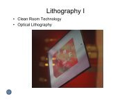
PHOTOLITHOGRAPHY
Photolithography…<br />
• Process of transferring geometrical<br />
patterns from mask on to layer of<br />
radiation sensitive material covering<br />
the surface of wafer.<br />
• Steps involved:<br />
• Coat wafer with resist.<br />
• Exposing to radiation.<br />
• Developing.<br />
• Etching.
MASK: Chrome coated quartz plate
Photo-resist<br />
• Is a radiation sensitive material which changes<br />
chemically on exposure to light.<br />
• Usually a carbon based organic molecule.<br />
• Two types of resist:<br />
– Positive<br />
• Regions of resist exposed to light dissolve quickly in<br />
‘developer’<br />
• Unexposed regions remain unchanged and are not removed<br />
by developer<br />
– Negative<br />
• Regions exposed to light are hard to remove by developer<br />
• Unexposed regions are easily removed by developer<br />
• Positive resists result in better resolution than<br />
negative resist
Positive <strong>Lithography</strong>
Negative <strong>Lithography</strong>
Mask:<br />
• Same size as final chip or an integral factor of<br />
final chip.<br />
• During exposure, the image size is reduced.<br />
• Made of fused silica.<br />
• Essential properties:<br />
– High degree of optical transparency.<br />
– Small thermal expansion coefficient.<br />
– Flat and polished surface.<br />
– Resistant to scratches.<br />
• Opaque layer: Chromium.
Aligning the masks<br />
• Each successive layer has to be<br />
aligned with the previous layer.<br />
• Each mask layer consists of<br />
alignment marks which help in aligning<br />
the layers on top of each other.
Features:<br />
• Resolution<br />
– Minimum feature size that can be<br />
transferred precisely.<br />
• Throughput<br />
– Number of wafers processed per hour.<br />
• Depth of focus<br />
– Masks must be aligned.
<strong>Lithography</strong> optical<br />
X-ray<br />
E-beam<br />
Contact printing<br />
Proximity printing<br />
Projection printing
Optical lithography<br />
• Most popular and oldest.<br />
• Follows four basic steps.<br />
• Contact printing:<br />
• Wafer in contact with mask.<br />
• High resolution.<br />
• Life of mask is less.<br />
• contamination
Optical lithography<br />
• Proximity printing:<br />
• Mask close to wafer.<br />
• No contact (10 to 25 μm)<br />
• Lesser resolution<br />
• Higher mask life.<br />
• Projection printing:<br />
• Mask kept at higher distance.<br />
• Highly focused image.<br />
• Higher mask life.<br />
• Compromise on cost.
E-beam lithography<br />
• Optical lithography: ~0.5 microns<br />
• For sub-micron fabrication: e-beam<br />
lithography.<br />
• Size < 1 μm possible.<br />
• Direct writing.<br />
• Easy automation.<br />
• Greater DOF.
HOW…<br />
• E-beam diameter: 0.01 to 0.5<br />
microns.<br />
• Focused on substrate.<br />
• Scanned over required area.<br />
• Substrate placed on movable table.<br />
– After one scan field, need to move<br />
wafer for next imprinting.
E-beam lithography<br />
• For higher resolution– smaller<br />
diameter.<br />
• Smaller diameter low throughput.<br />
• Minimum feature size ~ 4 x diameter.<br />
• Scan field ~ 2000 x diameter.<br />
• Hence higher time.
E-beam resist<br />
• Basically organic polymers.<br />
• 2 types : +ve and –ve<br />
• Positive resist<br />
• Softens with e-beam.<br />
• Chemical bond breaking.<br />
• Better resolution.<br />
• Poor sensitivity.
• Negative resist:<br />
• Hardens when exposed to radiations.<br />
• Cross-linking.<br />
• Increase in molecular weight.<br />
• Poor resolution due to swelling.
Issues regarding e-beam<br />
lithography<br />
• Slow process.<br />
• Proximity effect.<br />
• Due to electron scattering.<br />
• Inter proximity effect.<br />
• Intra proximity effect.<br />
• USED MAINLY FOR MASKS
X-ray lithography<br />
• An extension of optical lithography.<br />
• No direct writing.<br />
• Proximity printing.<br />
• Distance – 40 to 50 μm
Characteristics..<br />
• Faster throughput.<br />
• Good resolution.<br />
• No proximity effect.<br />
• No effect of dirt.<br />
• Straight walls due to low absorption.
HOW…<br />
• Electron beam focused to water cooled<br />
Palladium target.<br />
• Generates x-rays ( λ=4.37 angstrom)<br />
• Passed through beryllium window and sent<br />
to chamber.<br />
• Chamber filled with He.<br />
• He doesn’t absorb x-rays.<br />
• Mask and substrate kept at close<br />
proximity.<br />
• Substrate is developed by x-rays.
• Smaller λ higher resolution.<br />
• X-ray mask: thin membrane coated<br />
with gold.<br />
• All e-beam resist can be used as xray<br />
resist.<br />
• Mainly PMMA
Limitations<br />
• Geometric effects.<br />
• Mask is at a distance.<br />
• Instead of point, a blur region formed.<br />
• Depends on<br />
– Diameter of x-ray<br />
– Distance between mask and substrate.<br />
– Distance between light source and mask