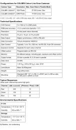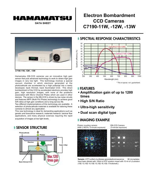
Electron Bombardment CCD Cameras C7190-11W, -12W, -13W
Electron Bombardment CCD Cameras C7190-11W, -12W, -13W
Electron Bombardment CCD Cameras C7190-11W, -12W, -13W

Create successful ePaper yourself
Turn your PDF publications into a flip-book with our unique Google optimized e-Paper software.
<strong>C7190</strong>-<strong>11W</strong>, -<strong>12W</strong> , -<strong>13W</strong><br />
<strong>Electron</strong><br />
DATA SHEET<br />
Hamamatsu EB-<strong>CCD</strong> cameras use an innovative high gain<br />
sensor that puts advanced technology to work to obtain high gain<br />
images in very low light. This technology involves a special<br />
vacuum chamber in which electrons generated at the<br />
photocathode are accelerated by a high potential into a newly<br />
developed, back thinned, back illunimated <strong>CCD</strong>. This direct<br />
bombardment of the <strong>CCD</strong> by accelerated electrons provides high<br />
gain, high resolution images, with none of the problems<br />
associated with Micro Channel Plates which are used in other<br />
devices. The sensor in the EB-<strong>CCD</strong> is driven by low noise circuits<br />
and features MPP (Multi Pin Phase) technology to achieve good<br />
S/N ratios at high gain conditions and a long service life.<br />
Two different implementations of this technology are available. A<br />
selection of photocathode materials is available for tailoring these<br />
cameras to almost any application.<br />
This new technology is ideal for demanding applications such as<br />
genetic and bioscience research, materials research, laminar flow<br />
applications, and many physical sciences requiring the rapid<br />
acquisition of images at low light levels.<br />
❚ SENSOR STRUCTURE<br />
Photocathode<br />
Back thinned <strong>CCD</strong><br />
Photon<br />
Accelerate<br />
Max.1200<br />
times gain<br />
Supply voltage<br />
Quantum efficiency (%)<br />
<strong>Electron</strong> <strong>Bombardment</strong><br />
<strong>CCD</strong> <strong>Cameras</strong><br />
<strong>C7190</strong>-<strong>11W</strong>, -<strong>12W</strong>, -<strong>13W</strong><br />
❚ SPECTRAL RESPONSE CHARACTERISTICS<br />
60<br />
55<br />
50<br />
45<br />
40<br />
35<br />
30<br />
25<br />
20<br />
S-20(<strong>C7190</strong>-<strong>11W</strong>)<br />
15<br />
10<br />
5<br />
0<br />
200 300 400 500 600 700 800 900 1000<br />
Wavelength (nm)<br />
* This is typical, not guaranteed.<br />
❚ FEATURES<br />
Amplification gain of up to 1200<br />
times<br />
High S /N Ratio<br />
Ultra-high sensitivity<br />
Dual scan digital type<br />
❚ IMAGING EXAMPLE<br />
Photon counting camera<br />
(With 2 MCPs: 5-minute exposure)<br />
GaAsP(<strong>C7190</strong>-<strong>13W</strong>)<br />
GaAs(<strong>C7190</strong>-<strong>12W</strong>)<br />
EB-<strong>CCD</strong> Camera<br />
(3-minute exposure)<br />
10 -13<br />
10 -14<br />
10 -15<br />
10 -16<br />
10 -17<br />
Sample: ATP luciferin-luciferase generatedluminescence. 96 microplates<br />
have been diluted with 100ml of ATP solution mixed with 10 ml of L/Lsolution.<br />
(10E-13,10E-14,10E-15,10E-16,10E-17mole/well,)
❚ SPECIFICATIONS<br />
˚<br />
Type. Number <strong>C7190</strong>-<strong>11W</strong> <strong>C7190</strong>-<strong>12W</strong> <strong>C7190</strong>-<strong>13W</strong><br />
<strong>CCD</strong> Structure Back thinned full frame transfer <strong>CCD</strong><br />
Total no. of pixels 512(H) × 512(V)<br />
Effective no. of pixels 512(H) × 512(V)<br />
Cell size 24 µm × 24 µm<br />
Effective area 12.3 mm × 12.3 mm / 1- inch format<br />
Readout noise 15 electrons r.m.s. (slow scan)<br />
Full well capacity 150,000 electrons (typ.)<br />
<strong>CCD</strong> dark current 8 electrons/pixel/s at -25˚ C<br />
Frame rate<br />
Slow scan: 3 Hz<br />
High scan: 5 Hz<br />
A/D converter<br />
Slow scan: 12 bit<br />
High scan: 12 bit<br />
Gate function 10 µsec<br />
Gain to 1200 times<br />
Sensitivity control Possible<br />
Low: 36 electrons/count<br />
System gain High: 15 electrons/count<br />
Super High: 4 electrons/count<br />
Cooling temperature -25 C<br />
Photocathode<br />
S-20 GaAs GaAsP<br />
Sensor structure Proximity focused type<br />
Data output RS-422 digital out<br />
Camera controller RS-232C<br />
Functions<br />
Dual mode readout / Contrast enhancement<br />
❚ DIMENSIONAL OUTLINES (Unit: mm)<br />
• Camera head (approx. 4.5 Kg) • Camera controller (approx. 10 Kg)<br />
120±0.5<br />
50±0.2<br />
60±0.5<br />
159±0.5<br />
C-mount<br />
261±1<br />
7.2 (C-mount)<br />
33<br />
30±0.2<br />
4-M4 D=6<br />
1/4-20UNC D=6<br />
40±0.2<br />
2-M6 D=6<br />
30±0.2<br />
POWER<br />
DUAL MODE COOLED <strong>CCD</strong> CAMERA C4880<br />
★ Product and software package names noted in this documentation are trademarks or registered trademarks of their respective manufacturers.<br />
● Subject to local technical requirements and regulations, availability of products included in this promotional material may vary. Please consult with our sales office. .<br />
● Information furnished by HAMAMATSU is believed to be reliable. However, no responsibility is assumed for possible inaccuracies or omissions.<br />
Specifications and external appearance are subject to change without notice.<br />
© 2003 Hamamatsu Photonics K.K.<br />
Homepage Address http://www.hamamatsu.com<br />
HAMAMATSU PHOTONICS K.K., Systems Division<br />
812 Joko-cho, Hamamatsu City, 431-3196, Japan, Telephone: (81)53-431-0124, Fax: (81)53-435-1574, E-mail:export@sys.hpk.co.jp<br />
U.S.A. and Canada: Hamamatsu Photonic Systems: 360 Foothill Road, Bridgewater, N.J. 08807-0910, U.S.A., Telephone: (1)908-231-1116, Fax: (1)908-231-0852, E-mail: usa@hamamatsu.com<br />
Germany: Hamamatsu Photonics Deutschland GmbH: Arzbergerstr. 10, D-82211 Herrsching am Ammersee, Germany, Telephone: (49)8152-375-0, Fax: (49)8152-2658, , E-mail: info@hamamatsu.de<br />
France: Hamamatsu Photonics France S.A.R.L.: 8, Rue du Saule Trapu, Parc du Moulin de Massy, 91882 Massy Cedex, France, Telephone: (33)1 69 53 71 00, Fax: (33)1 69 53 71 10, E-mail: infos@hamamatsu.fr<br />
United Kingdom: Hamamatsu Photonics UK Limited: 2 Howard Court, 10 Tewin Road, Welwyn Garden City, Hertfordshire, AL7 1BW, U.K., Telephone: (44) 1707-294888, Fax: (44) 1707-325777, E-mail: info@hamamatsu.co.uk<br />
North Europe: Hamamatsu Photonics Norden AB: Smidesvägen 12, SE-171-41 Solna, Sweden, Telephone: (46)8-509-031-00, Fax: (46)8-509-031-01, E-mail: - info@hamamatsu.se<br />
Italy: Hamamatsu Photonics Italia S.R.L.: Strada della Mois, 1/E 20020 Arese (Milano), Italy, Telephone: (39)02-935 81 733, Fax: (39)02-935 81 741, E-mail: info@hamamatsu.it<br />
SELECT RETURN<br />
350±1<br />
412±1<br />
MENU<br />
SUB<br />
MENU<br />
CONTRAST ENHANCEMENT<br />
GAIN<br />
MIN MAX<br />
OFFSET<br />
– 0<br />
6±1<br />
98.5±1<br />
3±0.5<br />
25±1<br />
325±1<br />
383±1<br />
EN ISO 9001:2000<br />
Certificate: 09 100 79045<br />
Cat. No. SICS1126E01<br />
APR/2004 HPK<br />
Created in Japan (PDF)