Wave Digital Filters - CCRMA - Stanford University
Wave Digital Filters - CCRMA - Stanford University
Wave Digital Filters - CCRMA - Stanford University

Create successful ePaper yourself
Turn your PDF publications into a flip-book with our unique Google optimized e-Paper software.
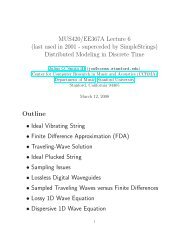
MUS420/EE367A Lecture 12<br />
<strong>Wave</strong> <strong>Digital</strong> <strong>Filters</strong><br />
Stefan Bilbao and Julius O. Smith III (jos@ccrma.stanford.edu)<br />
Center for Computer Research in Music and Acoustics (<strong>CCRMA</strong>)<br />
Department of Music, <strong>Stanford</strong> <strong>University</strong><br />
<strong>Stanford</strong>, California 94305<br />
Outline:<br />
January 6, 2013<br />
• Finite Difference Schemes<br />
• Delay Free Loops<br />
• <strong>Wave</strong> Variables<br />
• <strong>Wave</strong> <strong>Digital</strong> Inductor<br />
• Bilinear Transform<br />
• Scattering Junctions<br />
• Physical Derivation of <strong>Wave</strong> <strong>Digital</strong> <strong>Filters</strong><br />
• <strong>Wave</strong> <strong>Digital</strong> Resonator Exercise<br />
• Multidimensional <strong>Wave</strong> <strong>Digital</strong> <strong>Filters</strong> for solving<br />
PDEs<br />
1<br />
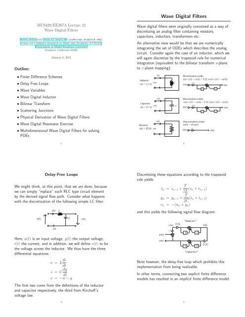
Delay-Free Loops<br />
We might think, at this point, that we are done, because<br />
we can simply “replace” each RLC type circuit element<br />
by the derived signal flow path. Consider what happens<br />
with the discretization of the following simple LC filter:<br />
i(t)<br />
u(t) C y(t)<br />
i(t)<br />
L<br />
Here, u(t) is an input voltage, y(t) the output voltage,<br />
i(t) the current, and in addition, we will define v(t) to be<br />
the voltage across the inductor. We thus have the three<br />
differential equations:<br />
v = L di<br />
dt<br />
i = C dy<br />
dt<br />
v = −u−y<br />
The first two come from the definitions of the inductor<br />
and capacitor respectively, the third from Kirchoff’s<br />
voltage law.<br />
3<br />
<strong>Wave</strong> <strong>Digital</strong> <strong>Filters</strong><br />
<strong>Wave</strong> digital filters were originally conceived as a way of<br />
discretizing an analog filter containing resistors,<br />
capacitors, inductors, transformers etc.<br />
An alternative view would be that we are numerically<br />
integrating the set of ODEs which describes the analog<br />
circuit. Consider again the case of an inductor, which we<br />
will again discretize by the trapezoid rule for numerical<br />
integration (equivalent to the bilinear transform s-plane<br />
to z-plane mapping):<br />
Inductor:<br />
v(t)<br />
v(t) = L i’(t)<br />
Capacitor:<br />
v(t)<br />
i(t) = Cv’(t)<br />
Resistor:<br />
v(t) = R i(t) v(t)<br />
i(t)<br />
i(t)<br />
i(t)<br />
L<br />
C<br />
Discretization yields:<br />
i((n+1)T) = i(nT) + T/2L (v((n+1)T) + v(nT))<br />
v(n)<br />
T/2L<br />
T<br />
T<br />
i(n)<br />
Discretization yields:<br />
v((n+1)T) = v(nT) + T/2C (i((n+1)T) + i(nT))<br />
i(n)<br />
T/2C<br />
Discretization yields:<br />
v(nT) = R i(nT)<br />
Discretizing these equations according to the trapezoid<br />
rule yields:<br />
i(n)<br />
2<br />
in = in−1+ T<br />
2L (vn+vn−1)<br />
yn = yn−1+ T<br />
2C (in+in−1)<br />
vn = −(un+yn)<br />
R<br />
T<br />
v(n)<br />
and this yields the following signal flow diagram:<br />
u(n)<br />
y(n)<br />
"inductor"<br />
v(n) T/2L<br />
i(n)<br />
-1<br />
T T<br />
T T<br />
"capacitor"<br />
T/2C<br />
Note however, the delay-free loop which prohibits this<br />
implementation from being realizable.<br />
In other terms, connecting two explicit finite difference<br />
models has resulted in an implicit finite difference model.<br />
4<br />
T<br />
v(n)
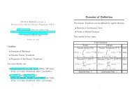
<strong>Wave</strong> Variables<br />
• In order to circumvent the problem of delay-free<br />
loops, Fettweis introduced wave variables:<br />
an = vn+inR0<br />
bn = vn−inR0<br />
where R0 is an arbitrary parameter called a port<br />
resistance (for reasons we’ll discuss later).<br />
• In matrix notation, we readily see that this is a linear<br />
transformation of the state variables {vn,in}:<br />
<br />
an 1 R0 vn<br />
=<br />
bn 1 −R0 in<br />
• Since the determinant of the two-by-two matrix is<br />
−2R0, the transformation is non-singular provided<br />
R0 = 0. We will additionally stipulate R0 > 0.<br />
• The inverse transformation is<br />
vn = an+bn<br />
2<br />
in = an−bn<br />
2R0<br />
Now there is no direct path from input to output.<br />
In terms of wave variables, with simplest choices of the<br />
port resistances, we obtain the following wave digital<br />
filter elements (the elementary one-ports):<br />
Inductor:<br />
v(t)<br />
v(t) = L i’(t)<br />
Capacitor:<br />
v(t)<br />
i(t) = Cv’(t)<br />
Resistor:<br />
v(t) = R i(t) v(t)<br />
i(t)<br />
i(t)<br />
i(t)<br />
L<br />
C<br />
5<br />
WD-Inductor:<br />
b(n) = - a(n-1)<br />
WD-Capacitor:<br />
b(n) = a(n-1)<br />
WD-Resistor:<br />
b(n) = 0<br />
Elementary wave-digital one-ports. The port impedances<br />
for the wave-digital inductor, capacitor, and resistor (on<br />
the right) are defined as 2L/T, T/(2C), and R,<br />
respectively.<br />
7<br />
a<br />
b<br />
a<br />
a<br />
b<br />
b<br />
-1<br />
T<br />
T<br />
Derivation of the <strong>Wave</strong> <strong>Digital</strong> Inductor<br />
It is instructive to see what happens when this change of<br />
variables in applied to the inductor.<br />
1. We have the following difference equation for the<br />
inductor (using the trapezoidal rule of numerical<br />
integration, or bilinear transform, as you prefer):<br />
in = in−1+ T<br />
2L (vn+vn−1)<br />
2. Perform the wave-variable substitution<br />
to get<br />
an−bn<br />
2R0<br />
vn = an+bn<br />
2<br />
in = an−bn<br />
2R0<br />
= an−1−bn−1<br />
+<br />
2R0<br />
T<br />
<br />
an+bn<br />
+<br />
2L 2<br />
an−1+bn−1<br />
<br />
2<br />
3. Now choose R0 = 2L/T to obtain<br />
an−bn = an−1−bn−1+(an+bn+an−1+bn−1)<br />
= 2an−1+an+bn<br />
which further simplifies to<br />
bn = −an−1 (<strong>Wave</strong> <strong>Digital</strong> Inductor)<br />
6<br />
Note on the Bilinear Transform<br />
1−z −1<br />
Recall the mapping s → 2<br />
T 1+z−1, which maps real<br />
frequencies to real frequencies. In fact, the mapping<br />
takes the RHP to the outside of the unit circle and the<br />
LHP to the inside. Thus:<br />
• Under this particular bilinear transform, a stable<br />
minimum phase continuous time system is mapped to<br />
a stable minimum phase discrete time system.<br />
• A function PR in the RHP is mapped to a function<br />
PR outside the unit circle.<br />
jω<br />
s plane<br />
bilinear xform<br />
z plane<br />
• Thus, in some sense this mapping preserves passivity<br />
or energetic properties of the original system.<br />
• This is the fundamental reason why it is used by<br />
Fettweis et al. as the basis for filter design and<br />
numerical integration.<br />
8
Building WDFs<br />
• These wave digital one-ports may now be connected<br />
(via scattering junctions, to match impedances) in<br />
order to simulate analog circuits, or, equivalently,<br />
mechanical systems of masses, springs and dashpots.<br />
• Since, in wave coordinates, there is no direct through<br />
path in any of the one-ports, delay-free loops cannot<br />
occur.<br />
• Since “passivity” is preserved under the bilinear<br />
transform, the filter/numerical integrator is<br />
guaranteed stable.<br />
9<br />
A Physical Derivation of <strong>Wave</strong> <strong>Digital</strong> <strong>Filters</strong><br />
• To each element, such as a capacitor or inductor,<br />
attach a length of transmission line at impedance R0,<br />
and make it infinitesimally long. (Take the limit as<br />
the length of the transmission line goes to zero.)<br />
– The infinitesimal transmission line is terminated by<br />
the element.<br />
– The line impedance is arbitrary because it has<br />
been physically introduced.<br />
– If two such line-augmented elements are connected<br />
together by their transmission lines, scattering will<br />
clearly be induced at the junction in the usual way.<br />
• Calculate the reflectance of the terminated line. That<br />
is, find the Laplace transform of the return wave<br />
divided by the Laplace transform of the input wave<br />
going into the line:<br />
– For a capacitor C (impedence RC(s) = 1/(Cs)),<br />
we get the reflectance<br />
SC(s) = (RC(s)−R0)/(RC(s)+R0), which<br />
simplifies to<br />
SC(s) = 1−R0Cs<br />
1+R0Cs<br />
11<br />
Scattering Junctions<br />
Suppose now that we would like to draw a new signal<br />
flow graph, using wave quantities. The problem now is<br />
that in general, the wave variables corresponding to a<br />
particular WD 1-port are scaled by different port<br />
resistances. So how do we connect them?<br />
a1<br />
b1<br />
?<br />
Port resistance R1 Port resistance R2<br />
We need to derive scattering equations...indeed,<br />
whenever we have an impedance change (even an artficial<br />
one such as this), we expect relection and transmission.<br />
10<br />
– For an inductor L, we get (Ls−R0)/(Ls+R0),<br />
or<br />
SL(s) = s−R0/L<br />
s+R0/L<br />
– For a resistor R, we get (R−R0)/(R+R0), or<br />
a2<br />
b2<br />
SR(s) = 1−R0/R<br />
1+R0/R<br />
– Note that both the capacitor and inductor<br />
reflectances are stable allpass filters, as they must<br />
be. Also, the resistor reflectance is always less than<br />
1, no matter what line impedance R0 we choose.<br />
• Observe that there is a natural choice for each<br />
transmission-line impedance which will give us a<br />
normalized, universal reflectance for each element:<br />
– For the capacitor, R0 = 1/C ⇒<br />
SC(s) = 1−s<br />
1+s<br />
– For the inductor, R0 = L ⇒<br />
SL(s) = − 1−s<br />
1+s<br />
– And for the resistor, R0 = R ⇒<br />
SR(s) = 0<br />
12
• Going to discrete time via the bilinear transform<br />
means making the substitution<br />
z −1<br />
s = c<br />
z +1<br />
where c is some arbitrary positive constant, usually<br />
taken to be c = 2/T.<br />
• Solving for z gives<br />
z = 1+s/c<br />
1−s/c<br />
• In this case, we see that setting c = 1 further<br />
simplifies our universal reflectances in the digital<br />
domain:<br />
– For the “wave digital capacitor” (or spring)<br />
<br />
z −1<br />
SC = z<br />
z +1<br />
−1<br />
– For the “wave digital inductor” (or mass)<br />
<br />
z −1<br />
SL = −z<br />
z +1<br />
−1<br />
– And for the “wave digital resistor” (or dashpot)<br />
<br />
z −1<br />
SR = 0<br />
z +1<br />
as before in the continuous-time case.<br />
13<br />
A <strong>Wave</strong> <strong>Digital</strong> Resonator Exercise<br />
Connect a wave digital capacitor and inductor together to<br />
form a second-order digital resonator consisting of<br />
• a scattering junction in the middle,<br />
• a unit-delay on the left (the capacitor), and<br />
• a unit-delay and -1 gain on the right (the inductor).<br />
You should be able to get a digital structure that looks<br />
like this:<br />
z −1<br />
1 + k<br />
k − k<br />
1 − k<br />
15<br />
− 1<br />
z −1<br />
Equivalently, we may obtain the same results by setting<br />
c = 2/T in the bilinear transform (which defines a<br />
frequency-scaling) and take the transmission-line (port)<br />
impedances to be instead RL = Lc = 2L/T for the<br />
inductor, and RC = T/(2C) for the capacitor (thereby<br />
compensating the frequency scaling).<br />
For the exercise,<br />
14<br />
Exercise, Cont.<br />
a) Find the reflection coefficient k of the induced<br />
scattering junction in terms of L and C.<br />
b) Find the poles in terms of k.<br />
c) Find the resonance frequency in terms of the sampling<br />
interval T and the reflection coefficient k.<br />
d) Recall that an analog LC loop resonates at 1/ √ LC,<br />
and relate these two resonance frequency formulas via<br />
the analog-digital frequency map ωa = tan(ωdT/2).<br />
e) Show that the trig identity you discovered in this way<br />
is true.<br />
This exercise verifies that the elementary “tank circuit”<br />
always resonates at exactly the frequency it should,<br />
according to the bilinear transform mapping.<br />
16
Features of <strong>Wave</strong> <strong>Digital</strong> <strong>Filters</strong> (and Bilinear<br />
Transforms)<br />
• We obtain an exact, one-to-one mapping of the<br />
frequency response S(jω) (a reflectance) to the unit<br />
circle in the z plane, even though each first-order<br />
element is reduced to a mere unit delay with a<br />
possible sign flip (or to nothing but 0 in the case of a<br />
resistor/dashpot).<br />
• One can show that a unit-sample delay in the digital<br />
version corresponds to an exactly correct phase-shift<br />
at the mapped analog frequency. The frequency<br />
mapping is, for this bilinear transform,<br />
<br />
ωdT<br />
ωa = tan ,<br />
2<br />
where ωa = analog radian frequency and ωd = digital<br />
radian frequency.<br />
• If it is possible to warp the frequencies of an input<br />
signal in the same way, that is, if we can perform the<br />
bilinear transform also on our analog input signal<br />
x(t) ↔ X(s)<br />
17<br />
A quick look at solving PDEs via<br />
Multi-dimensional WDFs<br />
Basic idea:<br />
Replace a system of PDEs by a set of Kirchoff Loop<br />
Equations, each of which contains multidimensional<br />
(distributed) circuit elements.<br />
Benefits:<br />
• Associates a passive set of equations with a passive<br />
electrical circuit ⇒ good stability properties.<br />
• Algorithm will be explicit, parallelizable<br />
• Extensions possible to non constant-coefficient,<br />
nonlinear problems, still retaining stability properties.<br />
Drawbacks:<br />
• Only works for PDEs derived from conservation<br />
relations (a small, but important class)<br />
• Convergence may be slow.<br />
Reference: Stefan Bilbao’s thesis 1<br />
1 http://ccrma.stanford.edu/~bilbao/<br />
19<br />
to produce a digital version<br />
<br />
z −1<br />
X ↔ xd(n),<br />
z +1<br />
then we can obtain exact LTI processing of an<br />
infinite-bandwidth signal inside a wave digital filter,<br />
no matter what sampling rate we choose!<br />
– Unfortunately, this is usually not possible.<br />
– Exercise: List the practical problems associated<br />
with trying to do something like this in practice,<br />
however approximate.<br />
• Because the frequency axis is warped, we cannot<br />
expect nonlinear or time-varying systems to behave in<br />
discrete time as they did in continuous time:<br />
– Modulation sidebands land at “wrong” frequencies.<br />
– Harmonic relationships are destroyed ⇒<br />
“harmonic distortion” becomes inharmonic.<br />
18<br />
Distributed Nonlinearities in Music<br />
• Shock waves in trombones<br />
• Gongs<br />
• Crashed cymbals<br />
• Turbulence in Flutes<br />
• Turbulence in the vocal tract<br />
20
Distributed Modeling Example: 1-D wave<br />
equation<br />
Let’s look at the continuity equations for the 1-D<br />
acoustic tube, in the linearized, adiabatic case:<br />
• Conservation of Mass:<br />
∂ρ<br />
= −∂(ρu)<br />
∂t ∂x<br />
• Conservation of Momentum:<br />
∂(ρu)<br />
= −c2∂ρ<br />
∂t ∂x<br />
Now, let us rename density ρ by a variable i1, and<br />
momentum density ρu by a variable i2, which we will<br />
associate with currents:<br />
∂i1<br />
= −∂i2<br />
∂t ∂x ,∂i2 = −c2∂i1<br />
∂t ∂x<br />
and finally:<br />
∂i1<br />
∂t<br />
∂i2<br />
+ = 0,∂i2<br />
∂x ∂t +c2∂i1 = 0<br />
∂x<br />
Now each ∂ ∂<br />
dt or dx applied to a “current” such as i1 or i2<br />
might be thought of as some sort of voltage<br />
corresponding to a generalized inductor (i.e., temporal or<br />
spatial). This is merely a way of making the jump to the<br />
following circuit representation of the equations:<br />
21<br />
-d/dt -d/dt<br />
i1<br />
d/dt<br />
i2<br />
c^2 d/dx d/dx<br />
• After a coordinate change, and impedance<br />
transformations (to remove negative inductances), we<br />
are left with a circuit that can be discretized<br />
according to WDF principles outlined above.<br />
• MD-WDF one-ports are simple generalizations of<br />
their 1-D equivalents, except that internal delays may<br />
include spatial steps as well.<br />
• Scattering is still memoryless (KCL equations depend<br />
only on voltage and current, not on the independent<br />
variuables).<br />
22