WT11 Datasheet - Glyn Store
WT11 Datasheet - Glyn Store
WT11 Datasheet - Glyn Store

Create successful ePaper yourself
Turn your PDF publications into a flip-book with our unique Google optimized e-Paper software.
8. LAYOUT AND SOLDERING CONSIDERATIONS<br />
8.1 Soldering recommendations<br />
<strong>WT11</strong> is compatible with industrial standard reflow profile for Pb-free solders. The reflow<br />
profile used is dependent on the thermal mass of the entire populated PCB, heat transfer<br />
efficiency of the oven and particular type of solder paste used. Consult the datasheet of<br />
particular solder paste for profile configurations.<br />
Bluegiga Technologies will give following recommendations for soldering the module to<br />
ensure reliable solder joint and operation of the module after soldering. Since the profile<br />
used is process and layout dependent, the optimum profile should be studied case by case.<br />
Thus following recommendation should be taken as a starting point guide.<br />
Refer to technical documentations of particular solder paste for profile configurations<br />
Avoid using more than one flow.<br />
Reliability of the solder joint and self-alignment of the component are dependent on<br />
the solder volume. Minimum of 150m stencil thickness is recommended.<br />
Aperture size of the stencil should be 1:1 with the pad size.<br />
A low residue, “no clean” solder paste should be used due to low mounted height of<br />
the component.<br />
8.2 Layout guidelines<br />
It is strongly recommended to use good layout practices to ensure proper operation of the<br />
module. Placing copper or any metal near antenna deteriorates its operation by having<br />
effect on the matching properties and the radiation efficiency. Metal shield around the<br />
antenna will prevent the radiation and thus metal case should not be used with the<br />
module.<br />
When using overlapping GND planes, use grounding vias separated max 3 mm apart at the<br />
edge of grounding areas to prevent RF penetrating inside the PCB and causing an<br />
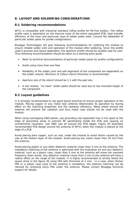
unintentional resonator. Use GND vias all around the PCB edges. Figure 30 illustrates<br />
recommended PCB design around the antenna of <strong>WT11</strong> when the module is placed at the<br />
edge of a PCB.<br />
Avoid placing bare copper, such as vias, under the module to avoid shorts caused by the<br />
vias at the bottom layer of the module. Avoid placing any metal closer than 20 mm from<br />
the antenna.<br />
Avoid placing plastic or any other dielectric material closer than 5 mm to the antenna. The<br />
impedance matching of the antenna is optimized with the evaluation kit and any dielectric<br />
material, such as a plastic case, closer than 5 mm to the antenna will move the resonant<br />
frequency down wards. Any dielectric material closer than 2 mm to the antenna will have a<br />
radical effect on the range of the module. It is highly recommended to strictly follow the<br />
layout show in the figure 30 using FR4 with thickness of 1 mm. In a case, when thicker<br />
FR4 or a plastic case close to the antenna is mandatory, the antenna matching can be<br />
retuned by removing extra FR4 under the antenna. Please contact Bluegiga technical<br />
support for details.<br />
41