WT11 Datasheet - Glyn Store
WT11 Datasheet - Glyn Store
WT11 Datasheet - Glyn Store

You also want an ePaper? Increase the reach of your titles
YUMPU automatically turns print PDFs into web optimized ePapers that Google loves.
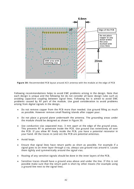
GND area with<br />
stitching vias<br />
42<br />
Edge of the PCB<br />
Do not place<br />
copper or any<br />
metal within<br />
the area<br />
marked with<br />
cross lines<br />
Figure 30: Recommended PCB layout around ACX antenna with the module at the edge of PCB<br />
Following recommendations helps to avoid EMC problems arising in the design. Note that<br />
each design is unique and the following list do not consider all basic design rules such as<br />
avoiding capacitive coupling between signal lines. Following list is aimed to avoid EMC<br />
problems caused by RF part of the module. Use good consideration to avoid problems<br />
arising from digital signals in the design.<br />
Do not remove copper from the PCB more than needed. Use ground filling as much<br />
as possible. However remove small floating islands after copper pour.<br />
Do not place a ground plane underneath the antenna. The grounding areas under<br />
the module should be designed as shown in Figure 30.<br />
Use conductive vias separated max. 3 mm apart at the edge of the ground areas.<br />
This prevents RF to penetrate inside the PCB. Use ground vias extensively all over<br />
the PCB. If you allow RF freely inside the PCB, you have a potential resonator in<br />
your hand. All the traces in (and on) the PCB are potential antennas.<br />
Avoid loops.<br />
Ensure that signal lines have return paths as short as possible. For example if a<br />
signal goes to an inner layer through a via, always use ground vias around it. Locate<br />
them tightly and symmetrically around the signal vias.<br />
Routing of any sensitive signals should be done in the inner layers of the PCB.<br />
Sensitive traces should have a ground area above and under the line. If this is not<br />
possible make sure that the return path is short by other means (for example using<br />
a ground line next to the signal line).