Winding Capacitance and Leakage Inductance
Winding Capacitance and Leakage Inductance
Winding Capacitance and Leakage Inductance

You also want an ePaper? Increase the reach of your titles
YUMPU automatically turns print PDFs into web optimized ePapers that Google loves.
Copyright © 2004 by Marcel Dekker, Inc. All Rights Reserved.<br />
Chapter 17<br />
<strong>Winding</strong> <strong>Capacitance</strong> <strong>and</strong> <strong>Leakage</strong> <strong>Inductance</strong>
1. Introduction<br />
2. Parasitic Effects<br />
3. <strong>Leakage</strong> Flux<br />
4. Minimizing <strong>Leakage</strong> <strong>Inductance</strong><br />
5. <strong>Winding</strong> <strong>Capacitance</strong><br />
6. <strong>Winding</strong> <strong>Capacitance</strong> Turn-to-Turn<br />
7. <strong>Winding</strong> <strong>Capacitance</strong> Layer-to-Layer<br />
8. <strong>Capacitance</strong> <strong>Winding</strong>-to-<strong>Winding</strong><br />
9. Stray <strong>Capacitance</strong><br />
10. References<br />
Copyright © 2004 by Marcel Dekker, Inc. All Rights Reserved.<br />
Table of Contents
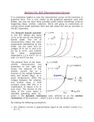
Introduction<br />
Operation of transformers at high frequencies presents unique design problems due to the increased<br />
importance of core loss, leakage inductance, <strong>and</strong> winding capacitance. The design of high frequency power<br />
converters is far less stringent than designing high frequency, wide-b<strong>and</strong> audio transformers. Operating at<br />
a single frequency requires fewer turns, <strong>and</strong> consequently, there is less leakage inductance <strong>and</strong> less<br />
capacitance with which to deal. The equivalent circuit for a two-winding transformer is shown in Figure<br />
17-1.<br />
R<br />
Lr<br />
Figure 17-1. Equivalent Transformer Circuit.<br />
High frequency designs require considerably more care in specifying the winding specification. This is<br />
because physical orientation <strong>and</strong> spacing of the windings determine leakage inductance <strong>and</strong> winding<br />
capacitance. <strong>Leakage</strong> inductance <strong>and</strong> capacitance are actually distributed throughout the winding in the<br />
transformer. However, for simplicity, they are shown as lumped constants, in Figure 17-1. The leakage<br />
inductance is represented by, Lp for the primary <strong>and</strong>, Ls for the secondary. The equivalent lumped<br />
capacitance is represented by, Cp <strong>and</strong> Cs for the primary <strong>and</strong> secondary windings. The dc winding<br />
resistance is, Rp, <strong>and</strong> Rs is for the equivalent resistance for the primary <strong>and</strong> secondary windings. Cw is the<br />
equivalent lumped, winding-to-winding capacitance. R,, is the equivalent core-loss shunt resistance.<br />
Parasitic Effects<br />
The effects of leakage inductance on switching power supplies' circuits are shown in Figure 17-2. The<br />
voltage spikes, shown in Figure 17-2, are caused by the stored energy in the leakage flux <strong>and</strong> will increase<br />
with load. These spikes will always appear on the leading edge of the voltage switching waveform.<br />
Copyright © 2004 by Marcel Dekker, Inc. All Rights Reserved.<br />
L,<br />
Energy = - '(Leak<br />
[watt-seconds] [17-1]
Transformers designed for switching applications are normally designed to have minimum leakage<br />
inductance, in order to minimize the voltage spikes, as shown in Figure 17-2. Also, leakage inductance can<br />
be observed by the leading edge slope of the trapezoidal current waveform.<br />
'on<br />
Actual<br />
Figure 17-2. Switching Transistor Voltage <strong>and</strong> Current Waveforms.<br />
Transformers designed for power conversion are normally being driven with a square wave, characterized<br />
by fast rise <strong>and</strong> fall times. This fast transition will generate high current spikes in the primary winding, due<br />
to the parasitic capacitance in the transformer. These current spikes, shown in Figure 17-3, are caused by<br />
the capacitance in the transformer; they will always appear on the lead edge of the current waveform <strong>and</strong><br />
always with the same amplitude, regardless of the load. This parasitic capacitance will be charged <strong>and</strong><br />
discharged every half cycle. Transformer leakage inductance <strong>and</strong> capacitance have an inverse relationship:<br />
if you decrease the leakage inductance, you will increase the capacitance; if you decrease the capacitance,<br />
you increase the leakage inductance. These are trade-offs that the power conversion engineer must make to<br />
design the best transformer for the application.<br />
T P Light Load Heavy Load<br />
Current Spike »•<br />
ton<br />
2<br />
ton<br />
-4 »•<br />
^<br />
^<br />
3<br />
ton<br />
•4 »-<br />
^<br />
4<br />
ton<br />
Ideal Actual Ideal Actual<br />
Figure 17-3. Transformer <strong>Capacitance</strong> Induced Current spike.<br />
<strong>Leakage</strong> Flux<br />
<strong>Leakage</strong> inductance is actually distributed throughout the windings of a transformer because of the flux set-<br />
up by the primary winding, which does not link the secondary, thus giving rise to leakage inductance in<br />
each winding without contributing to the mutual flux, as shown in Figure 17-4.<br />
Copyright © 2004 by Marcel Dekker, Inc. All Rights Reserved.
However, for simplicity, leakage inductance is shown as a lumped constant in Figure 17-1, where the<br />
leakage inductance is represented by Lp.<br />
<strong>Leakage</strong> Flux —<br />
EE Core ^<br />
c=:^^^^^^=<br />
-^<br />
— *"Ls<br />
-r-^s<br />
•^ c<br />
^c<br />
C<br />
|=ii=^^^l<br />
/<br />
^^^^<br />
•s* -i<br />
r=-<br />
E5 ~<br />
—<br />
3<br />
><br />
><br />
Figure 17-4. <strong>Leakage</strong> Flux.<br />
^<br />
Primary<br />
Secondary<br />
In the layer-wound coil, a substantial reduction in leakage inductance, Lp <strong>and</strong> Ls, is obtained by<br />
interweaving the primary <strong>and</strong> secondary windings. The st<strong>and</strong>ard transformer, with a single primary <strong>and</strong><br />
secondary winding, is shown in Figure 17-5, along with its leakage inductance, Equation [17-2]. Taking<br />
the same transformer <strong>and</strong> splitting the secondary on either side of the primary will reduce the leakage<br />
inductance, as shown in Figure 17-6, along with its leakage inductance, Equation [17-3]. The leakage<br />
inductance can be reduced even more, by interleaving the primary <strong>and</strong> secondary, as shown in Figure 17-7,<br />
along with its leakage inductance, Equation [17-4]. Transformers can also be constructed using the side-<br />
by-side, sectionalized bobbin as shown in Figure 17-8, along with its leakage inductance, Equation [17-5].<br />
The modified three section, side-by-side bobbin is shown in Figure 17-9, along with its leakage inductance<br />
Equation [ 17-6].<br />
EE Core *-<br />
<strong>Winding</strong> Area<br />
Core Mating Surface— *-<br />
Mutual Flux<br />
Window —<br />
Copyright © 2004 by Marcel Dekker, Inc. All Rights Reserved.<br />
»-<br />
— -*-<br />
Primary ~~*"<br />
££<br />
1 II1<br />
...,<br />
-».<br />
t<br />
a = <strong>Winding</strong> length, cm<br />
a b = <strong>Winding</strong> build, cm<br />
c = Insulation thickness, cm<br />
\ '<br />
\<br />
H Secondary<br />
J\<br />
Insulation<br />
Figure 17-5. Conventional Transformer Configuration.
EE Core »•<br />
\Vinding Area<br />
Core Mating Surface — *-<br />
Mutual Flux *-<br />
Window —<br />
— \ ^*-<br />
V<br />
1EB^^^<br />
W////M/A<br />
H~<br />
,- Primary<br />
^"i<br />
| \<br />
s<br />
\ a = <strong>Winding</strong> length, cm<br />
s,<br />
s a b = <strong>Winding</strong> build, cm<br />
1<br />
c = Insulation thickness, cm<br />
\ _ Insulation<br />
\<br />
Ns/2 Secondary each<br />
b!-,|1<br />
•4<br />
b2 -b3 ^<br />
c c<br />
Figure 17-6. Conventional, Transformer Configuration with Simple Interleave.<br />
EE Core *-<br />
Core Mating Surface — *-<br />
Lp= n(MLT\N2<br />
{ > "<br />
Mutual Flux »•<br />
l_^___£<br />
Window — — n*.<br />
\ •<br />
V<br />
I<br />
If^<br />
\<br />
\<br />
Ib b b b<br />
c c c<br />
X , [henrys] [17-3]<br />
^ i<br />
\<br />
1<br />
\<br />
Np/2 Primary each<br />
a = <strong>Winding</strong> length, cm<br />
a b = <strong>Winding</strong> build, cm<br />
c = Insulation thickness, cm<br />
Insulation<br />
Ns/2 Secondary each<br />
Figure 17-7. Sectionalized, Transformer Configuration Primary <strong>and</strong> Secondary Interleave.<br />
EE Core<br />
Bobbin<br />
<strong>Winding</strong> Area •<br />
Core Mating Surface<br />
Mutual Flux<br />
Window<br />
— *•<br />
Copyright © 2004 by Marcel Dekker, Inc. All Rights Reserved.<br />
?<br />
»•<br />
-**• s<br />
<<br />
\<br />
1 f<br />
-H b<br />
... V..I<br />
/<br />
y<br />
=*=<br />
\> N<br />
^ —<br />
' Secondary<br />
i<br />
a<br />
\ r± a = <strong>Winding</strong> length, cm<br />
JT- c b - <strong>Winding</strong> build, cm<br />
a c = Insulation thickness, cm<br />
^ Insulation<br />
x Primary<br />
Figure 17-8. Pot Core, Sectionalized Transformer Configuration.<br />
4x(MLT)N 2<br />
V ^ " (l(T 9 ), [henrys] [17-5]
EE Core<br />
Bobbin<br />
<strong>Winding</strong> Area<br />
Core Mating Surface<br />
Mutual Flux<br />
Window<br />
Secondary<br />
0 a = <strong>Winding</strong> length, cm<br />
a b = <strong>Winding</strong> build, cm<br />
c = Insulation thickness, cm<br />
Insulation<br />
Np/2 Primary<br />
Figure 17-9. Modified, Pot Core Sectionalized, Transformer Configuration.<br />
7r(MLT}Nl( Za\ «A<br />
Lp= V ' ' Zc + — (KT 9 ), [henrys] [17-6]<br />
b I 3 j v<br />
Minimizing <strong>Leakage</strong> <strong>Inductance</strong><br />
Magnetic core geometry has a big influence on leakage inductance. To minimize leakage inductance, the<br />
primary winding should be wound on a long bobbin, or tube, with the secondary wound as close as<br />
possible, using a minimum of insulation. Magnetic cores can have identical rating, but one core will<br />
provide a lower leakage inductance than the other. A simple comparison would be two cores with the same<br />
window area, but one core has twice the winding length. Only half the winding build is shown in Figure<br />
17-10.<br />
EE Cores. Bobbin<br />
\ /<br />
Secondary<br />
Primary /<br />
Special Long Tongue EE Core St<strong>and</strong>ard EE Core Configuration<br />
Bobbin<br />
EE Cores<br />
Figure 17-10. Comparing a St<strong>and</strong>ard EE Core <strong>and</strong> a Special Long Tongue Core.<br />
If layers must be used, the only way to reduce the leakage inductance is to divide the primary winding into<br />
sections, <strong>and</strong> then to s<strong>and</strong>wich the secondary winding between them, as shown in Figure 17-7. This can<br />
pose a real problem when designing around the European VDE specification, because of the required<br />
creepage distance <strong>and</strong> the minimum insulation requirements between the primary <strong>and</strong> secondary.<br />
Minimizing the leakage inductance on a push-pull converter design could be a big problem. A special<br />
consideration is required symmetry in both the leakage inductance <strong>and</strong> dc resistance; this is in order to get a<br />
balanced winding for the primary switching circuit to function properly.<br />
Copyright © 2004 by Marcel Dekker, Inc. All Rights Reserved.
The best way to minimize the leakage inductance, <strong>and</strong> to have a balanced dc resistance in a push-pull or<br />
center-tapped winding, is to wind bifilar. Bifilar windings will drastically reduce leakage inductance. This<br />
condition also exists on the secondary, when the secondary is a full-wave, center-tapped circuit. A bifilar<br />
winding is a pair of insulated wires, wound simultaneously <strong>and</strong> contiguously, (i.e., close enough to touch<br />
each other); Warning: do not use bifilar wire or the capacitance will go out of sight. Each wire constitutes a<br />
winding; their proximity reduces leakage inductance by several orders of magnitude, more than ordinary<br />
interleaving. This arrangement can be applied to the primary, to the secondary, or, it can be applied to the<br />
primary <strong>and</strong> secondary together. This arrangement will provide the minimum leakage inductance.<br />
<strong>Winding</strong> <strong>Capacitance</strong><br />
Operating at high frequency presents unique problems in the design of transformers to minimize the effect<br />
of winding capacitance. Transformer winding capacitance is detrimental in three ways: (1) winding<br />
capacitance can drive the transformer into premature resonance; (2) winding capacitance can produce large<br />
primary current spikes when operating from a square wave source, (3) winding capacitance can produce<br />
electrostatic coupling to other circuits.<br />
When a transformer is operating, different voltage gradients arise almost everywhere. These voltage<br />
gradients are caused by a large variety of capacitance throughout the transformer, due to the turns <strong>and</strong> how<br />
they are placed throughout the transformer. When designing high frequency converters, there are several<br />
factors that have a control over the turns: (1) the operating flux density or core loss; (2) the operating<br />
voltage levels in the primary <strong>and</strong> secondary; (3) the primary inductance.<br />
Keeping turns to a minimum will keep the capacitance to a minimum. This capacitance can be separated<br />
into four categories: (1) capacitance between turns; (2) capacitance between layers; (3) capacitance<br />
between windings; <strong>and</strong> (4) stray capacitance. The net effect of the capacitance is normally seen by the<br />
lumped capacitance, Cp, on the primary, as shown in Figure 17-1. The lumped capacitance is very difficult<br />
to calculate by itself. It is much easier to measure the primary inductance <strong>and</strong> the resonant frequency of the<br />
transformer or inductor, as shown in Figure 17-11. Then, calculate the capacitance using Equation [17-7].<br />
The test circuit, in Figure 17-11 functions as follows: The input voltage, VI, is held constant while<br />
monitoring the voltage, V2, sweep through the frequency with the power oscillator. When the voltage, V2,<br />
rises to a peak, <strong>and</strong> starts to decay at this peak voltage, the transformer or inductor is in resonance. At this<br />
point the phase angle is also 0 degrees at resonance when looking at both the curves of VI <strong>and</strong> V2.<br />
Copyright © 2004 by Marcel Dekker, Inc. All Rights Reserved.<br />
Ca = —~ = ———, [farads] [17-7]<br />
' '
Power Audio Oscillator<br />
Vert #2 Input Voltage<br />
Vert. #1, VI<br />
Vert. #2, V2<br />
Dual Channel Oscilloscope<br />
UUT<br />
Figure 17-11. Circuit for Measuring either a Transformer or Inductor Self Resonates.<br />
For transformers designed to operate with a square wave, such as dc-to-dc converter, leakage inductance,<br />
Lp, <strong>and</strong> the lumped capacitance, Cp, should be kept to a minimum. This is because they cause overshoot<br />
<strong>and</strong> oscillate, or ring, as shown in Figure 17-12. The overshoot oscillation, seen in Figure 17-12A, has a<br />
resonant frequency, f, that is controlled by, Lp <strong>and</strong> Cp. This resonant frequency could change <strong>and</strong> change<br />
drastically after potting, depending on the material <strong>and</strong> its dielectric constant, as shown Figure 17-12B.<br />
Copyright © 2004 by Marcel Dekker, Inc. All Rights Reserved.<br />
(17-12-A) (17-12-B)<br />
Figure 17-12. Primary Voltage with Leading Edge Ringing.
<strong>Winding</strong> <strong>Capacitance</strong> Turn-to-Turn<br />
The turn-to-turn capacitance, Cb, shown in Figure 17-13, should not be a problem if you are operating at<br />
high frequency, low voltage power converters, due to the low number of turns. If the turn-to-turn<br />
capacitance is important, then change the magnet wire insulation to one with a lower dielectric constant.<br />
See Chapter 4.<br />
'<br />
Cp<br />
Primary f<br />
r» ,<br />
C t<br />
s~<br />
C t<br />
f^<br />
-~^<br />
s~ -><br />
~> N p<br />
s ^J<br />
cs<br />
^<br />
Figure 17-13. <strong>Capacitance</strong> Turn-to-Turn.<br />
<strong>Winding</strong> <strong>Capacitance</strong> Layer-to-Layer<br />
s<br />
o<br />
Secondary<br />
The capacitance between layers on the primary or secondary is the best contributor to the overall, lumped<br />
capacitance, Cp. There are three ways to minimize the layer capacitance: (1) Divide the primary <strong>and</strong><br />
secondary windings into sections, <strong>and</strong> then s<strong>and</strong>wich the other winding between them, as shown in Figure<br />
17-7; (2) The foldback winding technique, shown in Figure 17-14, is preferred to the normal U type<br />
winding, even though it takes an extra step before starting the next layer. The foldback winding technique<br />
will also reduce the voltage gradient between the end of the windings; (3) Increasing the amount of<br />
insulation between windings will decrease the amount of capacitance. But remember, this will increase the<br />
leakage inductance. If the capacitance is reduced, then the leakage inductance will go up. There is one<br />
exception to this rule, <strong>and</strong> that is, if the windings are s<strong>and</strong>wiched or interleaved, it will reduce the winding<br />
capacitance, but, it will increase the winding-to-winding capacitance.<br />
Copyright © 2004 by Marcel Dekker, Inc. All Rights Reserved.<br />
Foldback <strong>Winding</strong> U Type <strong>Winding</strong><br />
Figure 17-14. Comparing the Foldback to the U Type <strong>Winding</strong>.<br />
r>
Transformers <strong>and</strong> inductors wound on toroidal cores can have capacitance problems, just as much if care is<br />
not taken in the design at the beginning. It is difficult to control the winding capacitance on a toroidal core<br />
because of its odd configuration, but there are ways to control the windings <strong>and</strong> capacitance. The use of<br />
tape barriers to mark a zone for windings, as shown in Figure 17-15, offers a good way to control this<br />
capacitance.<br />
Tape Barrier<br />
<strong>Winding</strong> area<br />
- Toroidal Core<br />
Figure 17-15. Tape Barrier for <strong>Winding</strong> Toroidal Core.<br />
Another way to help reduce the capacitance effect on toroids is to use the progressive winding technique.<br />
The progressive winding technique example is shown in Figure 17-16 <strong>and</strong> 17-17: Wind 5 turns forward <strong>and</strong><br />
wind 4 turns back, then wind 10 turns forward <strong>and</strong> keep repeating this procedure until the winding is<br />
complete.<br />
Continuous winding<br />
Core<br />
Figure 17-16. Progress <strong>Winding</strong> Top View.<br />
Back Wind<br />
Exp<strong>and</strong>ed View<br />
Figure 17-17. Progress <strong>Winding</strong> Side View.<br />
<strong>Capacitance</strong> <strong>Winding</strong>-to-winding<br />
Back wind<br />
Balanced windings are very important in keeping down noise <strong>and</strong> common mode signals that could lead to<br />
in-circuit noise <strong>and</strong> instability problems later on. The capacitance, from winding-to-winding, shown in<br />
Figure 17-18, can be reduced, by increasing the amount of insulation between windings. This will decrease<br />
the amount of capacitance, but again, this will increase the leakage inductance. The capacitance effect<br />
Copyright © 2004 by Marcel Dekker, Inc. All Rights Reserved.
etween windings can be reduced, without increasing the leakage inductance noticeably. This can be done,<br />
by adding a Faraday Shield or screen, as shown in Figure 17-19, between primary <strong>and</strong> secondary windings.<br />
A Faraday Shield is an electrostatic shield, usually made of copper foil. The Faraday Shield is normally<br />
added along with the insulation between primary <strong>and</strong> secondary. In some designs, the Faraday Shield can<br />
consist of three independent insulated shields or just one. It all depends on the required noise rejection.<br />
Primary Secondary<br />
Figure 17-18. <strong>Capacitance</strong>, Cw, <strong>Winding</strong>-to-<strong>Winding</strong>.<br />
Primary<br />
Shield #1<br />
Secondary<br />
Shield #2<br />
Figure 17-19. Transformer with a Primary <strong>and</strong> Secondary Shield.<br />
Stray <strong>Capacitance</strong><br />
Stray capacitance is very important to minimize because it too, can generate asymmetry currents <strong>and</strong> could<br />
lead to high common mode noise. Stray capacitance is similar to winding-to-winding capacitance except<br />
that the capacitance is between the winding next to the core, Cc, <strong>and</strong> the outer winding next to the<br />
surrounding circuitry, Cs, as shown in Figure 17-20. Stray capacitance can be minimized by using a<br />
balanced winding, or using a copper shield over the entire winding. A means for measuring leakage current<br />
is shown in Figure 17-21. The winding-to-winding capacitance can be calculated, using Equations [17-8]<br />
<strong>and</strong> [17-9].<br />
Copyright © 2004 by Marcel Dekker, Inc. All Rights Reserved.<br />
C = -, [farads] [17-9]
Core -Surrounding Circuitry<br />
Electrostatic<br />
Figure 17-20. Transformer <strong>Winding</strong> with Stray <strong>Capacitance</strong>.<br />
Power Audio Oscillator Digital Voltmeter<br />
Frequency<br />
1 1 1 1 I I I I I I I I 1 1 1 1 1 1 1 1<br />
Voltage<br />
Copyright © 2004 by Marcel Dekker, Inc. All Rights Reserved.<br />
Figure 17-21. Test Circuit for Measuring Primary <strong>and</strong> Secondary, ac <strong>Leakage</strong> Current.
References<br />
1. Grossner, N., "Transformer for Electronic Circuits." McGraw-Hill, New York, 1967.<br />
2. L<strong>and</strong>ee, R., Davis, D., <strong>and</strong> Albecht, A., "Electronic Designer's H<strong>and</strong>book," McGraw-Hill, New York,<br />
1957, p. 17-12.<br />
3. Lee, R., "Electronic Transformer <strong>and</strong> Circuits," 2 nd ed., John Wiley & Sons, New York, 1958.<br />
"Reference Data for Radio Engineers," 4 th ed., International Telephone <strong>and</strong> Telegraph Co., New York.<br />
4. Richardson, I., The Technique of Transformer Design, Electro-Technology, January 1961, pp. 58-67.<br />
Flanagan, W., "H<strong>and</strong>book of Transformer Application." McGraw-Hill, New York, 1986.<br />
Copyright © 2004 by Marcel Dekker, Inc. All Rights Reserved.