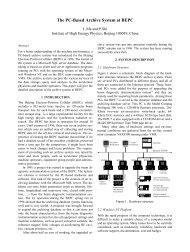
PZ004 - KEK
PZ004 - KEK
PZ004 - KEK

You also want an ePaper? Increase the reach of your titles
YUMPU automatically turns print PDFs into web optimized ePapers that Google loves.
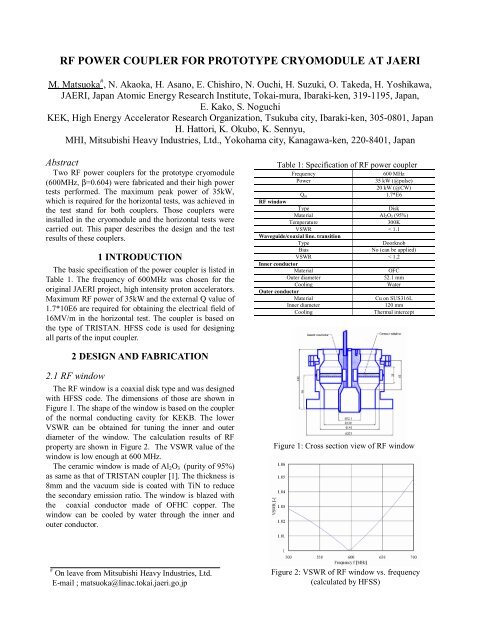
RF POWER COUPLER FOR PROTOTYPE CRYOMODULE AT JAERI<br />
M. Matsuoka # , N. Akaoka, H. Asano, E. Chishiro, N. Ouchi, H. Suzuki, O. Takeda, H. Yoshikawa,<br />
JAERI, Japan Atomic Energy Research Institute, Tokai-mura, Ibaraki-ken, 319-1195, Japan,<br />
E. Kako, S. Noguchi<br />
<strong>KEK</strong>, High Energy Accelerator Research Organization, Tsukuba city, Ibaraki-ken, 305-0801, Japan<br />
H. Hattori, K. Okubo, K. Sennyu,<br />
MHI, Mitsubishi Heavy Industries, Ltd., Yokohama city, Kanagawa-ken, 220-8401, Japan<br />
Abstract<br />
Two RF power couplers for the prototype cryomodule<br />
(600MHz, β=0.604) were fabricated and their high power<br />
tests performed. The maximum peak power of 35kW,<br />
which is required for the horizontal tests, was achieved in<br />
the test stand for both couplers. Those couplers were<br />
installed in the cryomodule and the horizontal tests were<br />
carried out. This paper describes the design and the test<br />
results of these couplers.<br />
1 INTRODUCTION<br />
The basic specification of the power coupler is listed in<br />
Table 1. The frequency of 600MHz was chosen for the<br />
original JAERI project, high intensity proton accelerators.<br />
Maximum RF power of 35kW and the external Q value of<br />
1.7*10E6 are required for obtaining the electrical field of<br />
16MV/m in the horizontal test. The coupler is based on<br />
the type of TRISTAN. HFSS code is used for designing<br />
all parts of the input coupler.<br />
2 DESIGN AND FABRICATION<br />
2.1 RF window<br />
The RF window is a coaxial disk type and was designed<br />
with HFSS code. The dimensions of those are shown in<br />
Figure 1. The shape of the window is based on the coupler<br />
of the normal conducting cavity for <strong>KEK</strong>B. The lower<br />
VSWR can be obtained for tuning the inner and outer<br />
diameter of the window. The calculation results of RF<br />
property are shown in Figure 2. The VSWR value of the<br />
window is low enough at 600 MHz.<br />
The ceramic window is made of Al2O3 (purity of 95%)<br />
as same as that of TRISTAN coupler [1]. The thickness is<br />
8mm and the vacuum side is coated with TiN to reduce<br />
the secondary emission ratio. The window is blazed with<br />
the coaxial conductor made of OFHC copper. The<br />
windowcanbecooledbywaterthroughtheinnerand<br />
outer conductor.<br />
# On leave from Mitsubishi Heavy Industries, Ltd.<br />
E-mail ; matsuoka@linac.tokai.jaeri.go.jp<br />
Table 1: Specification of RF power coupler<br />
Frequency 600 MHz<br />
Power 35 kW (@pulse)<br />
Qin<br />
20 kW (@CW)<br />
1.7*E6<br />
RF window<br />
Type Disk<br />
Material Al2O3 (95%)<br />
Temperature 300K<br />
VSWR<br />
Waveguide/coaxial line. transition<br />
< 1.1<br />
Type Doorknob<br />
Bias No (can be applied)<br />
VSWR<br />
Inner conductor<br />
< 1.2<br />
Material OFC<br />
Outer diameter 52.1 mm<br />
Cooling<br />
Outer conductor<br />
Water<br />
Material Cu on SUS316L<br />
Inner diameter 120 mm<br />
Cooling Thermal intercept<br />
Figure 1: Cross section view of RF window<br />
Figure 2: VSWR of RF window vs. frequency<br />
(calculated by HFSS)
2.2 Transition from waveguide to coaxial line<br />
The transition from waveguide to coaxial line is a<br />
doorknob type. The shape of the doorknob is based on the<br />
type of TRISTAN[1] and scaled according to the<br />
frequency. The dimensions were shown in figure 3. DC<br />
bias between the inner conductor and the outer conductor<br />
can be applied. The characteristics of the RF transmission<br />
are calculated as shown in figure 4.<br />
2.3 Inner conductor<br />
The inner conductor shown in Figure 5 is made of<br />
OFHC and has a cooling pass inside. The outer diameter<br />
is 52.1 mm as same as 120D coaxial line. The length is<br />
determined by coupling to 5-cell cavity (β=0.604). The<br />
smoothness of the surface is obtained by the electropolishing.<br />
Then inner conductor was welded with the RF<br />
window by EBW (Electron Beam Welding). Just before<br />
assembling with the outer conductor, the inner conductors<br />
and the RF windows were rinsed by ultra pure water in a<br />
clean room (Class 100).<br />
2.4 Outer conductor<br />
The outer conductor is made of stainless steel<br />
(SUS316L), and coated with copper inside. The thermal<br />
intercepts are on the outside to cool and reduce the heat<br />
load into the cryostat. Ultra pure rinsing was carried out<br />
as same as the inner conductor.<br />
Figure 3: Cross section view of doorknob<br />
Figure 4: VSWR of doorknob vs. frequency<br />
(Calculated by HFSS)<br />
RF window<br />
Inner conductor<br />
Figure 5: Inner conductor and RF window<br />
2.5 Coupling cavity<br />
The coupling cavity is fabricated for the high power test<br />
of the input coupler. The cavity is a rectangular type made<br />
of stainless steel (SUS304) and is coated with copper<br />
inside. The length of the cavity and the position of the<br />
inner conductor is determined by calculation with HFSS.<br />
3 LOW POWER TEST<br />
3.1 RF window<br />
RF transmission performances of the windows were<br />
measured with a network analyser. The result is shown in<br />
Table 2. VSWR values of the windows are under 1.1. The<br />
characteristics are deferent from the calculation results<br />
because the electrical connection between the RF window<br />
and the coaxial line was not enough.<br />
3.2 Doorknob<br />
RF transmission performances of the doorknob were<br />
measured with a network analyser as same as the RF<br />
window. The result is shown in Table 2. VSWR values of<br />
the windows are under 1.2.<br />
3.3 Input coupler with coupling cavity<br />
VSWR is not enough good as shown in Table 2. This is<br />
the reason why there is a different dimension between the<br />
basic design and the fabrication. The calculation results of<br />
the actual fabricated model are consistent with the<br />
measurement results.<br />
Table 2: Summary of low power test<br />
No.1 No.2<br />
RF window<br />
VSWR 1.1 1.1<br />
Doorknob<br />
VSWR 1.2 1.2<br />
Test stand<br />
VSWR (without doorknob) 1.2<br />
VSWR (with doorknob) 1.4<br />
Set up for horizontal test<br />
Qin 1.2E6 1.1E6
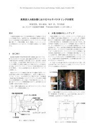
4 HIGH POWER TEST<br />
IOT (Inductive Output Tube) was adapted for an RF<br />
power source. To obtain the stable RF pulse, PLL and<br />
ALC system, which is for RF control of TRISTAN’s<br />
superconducting cavity, were prepared. The vacuum<br />
system consists of a turbo molecular pump and a rotary<br />
pump. A vacuum sensor and an arc sensor are located the<br />
side of each window. One can observe the partial pressure<br />
using by the mass spectrum analyser. Figure 6 is a<br />
photograph of the high power test stand.<br />
The results of the high power test are listed in Table 4.<br />
Under all the conditions, the sufficient results were<br />
obtained. The feature of the reflected power depending on<br />
the input power is shown in Figure 7. The ratio between<br />
reflection and input power is about 3% in this system.<br />
The RF loss measured by the temperature rise of cooling<br />
water is about 130W for two windows and inner<br />
conductors at the transmitted power of 35kW. Figure 8<br />
shows the typical time chart in the RF processing. The<br />
pressure rising began at the transmitted power of about<br />
12kW and hydrogen gas was observed during the RF<br />
processing as shown in figure 9.<br />
5 CONCLUSIONS<br />
The input couplers for the 600MHz cryomodule<br />
achieved the maximum input power of 35kW. These<br />
couplers were installed in the cryomodule and the<br />
horizontal test was carried out [3].<br />
Table 4: Summary of high power test results<br />
RF terminal condition<br />
And operational mode<br />
Dummy load<br />
RF power Conditioning time<br />
CW 35 kW 3.8 H<br />
Pulse<br />
Perfect reflection<br />
35 kW 7.3 H<br />
CW 20 kW 0.8 H<br />
Pulse 35 kW 1.4 H<br />
Perfect reflection +<br />
waveguide (λ/4)<br />
CW 20 kW 0.5 H<br />
Pulse<br />
In cryomodule<br />
35 kW 2.8 H<br />
CW 20 kW 0.5 H (#1),0.5 H (#2)<br />
Pulse 35 kW 4.0 H (#1),2.0 H (#2)<br />
Input coupler<br />
Q-mass<br />
Vacuum pump<br />
Vacuum sensor<br />
Coupling cavity<br />
Figure 6: High power test stand<br />
REFFERENCES<br />
[1] S. Noguchi, et al., “COUPLERS-EXPERIENCE AT<br />
<strong>KEK</strong>-”, Proc. of the 4 th Workshop on RF<br />
Superconductivity, 1989, pp.397-412.<br />
[2] E. Chishiro et al., “Evaluation of Operating<br />
Characteristics of IOT RF Source”, 24 th Linear<br />
accelerator meeting in Japan, 1999,<br />
[3] N. Ouchi, et al., “600MHz PROTOTYOE<br />
CRYOMODULE FOR HIGH INTENSITY<br />
PROTON LINAC AT JAERI “, in this meeting.<br />
Amplitude [arb. unit]<br />
Amplitude [arb. unit]<br />
300<br />
250<br />
200<br />
150<br />
100<br />
50<br />
0<br />
300<br />
250<br />
200<br />
150<br />
100<br />
50<br />
0<br />
H 2<br />
Figure 7 Reflection power vs. input power<br />
Figure 8 Time chart of RF processing<br />
H 2 O<br />
N 2 ,CO<br />
CO 2<br />
1 11 21 31 41 51<br />
M ass number [-]<br />
H 2<br />
H 2 O<br />
N 2 ,CO<br />
During baking<br />
During RF processing<br />
1 11 21 31 41<br />
M ass number [-]<br />
Figure 9: Mass spectrum at high power test stand<br />
CO 2