Analog Dialogue Volume 40, Number2, 2006
Analog Dialogue Volume 40, Number2, 2006
Analog Dialogue Volume 40, Number2, 2006

You also want an ePaper? Increase the reach of your titles
YUMPU automatically turns print PDFs into web optimized ePapers that Google loves.
Class D Audio Amplifiers:<br />
What, Why, and How<br />
By Eric Gaalaas [eric.gaalaas@analog.com]<br />
Class D amplifiers, first proposed in 1958, have become<br />
increasingly popular in recent years. What are Class D amplifiers?<br />
How do they compare with other kinds of amplifiers? Why is<br />
Class D of interest for audio? What is needed to make a “good”<br />
audio Class D amplifier? What are the features of ADI’s Class D<br />
amplifier products? Find the answers to all these questions in the<br />
following pages.<br />
Audio Amplifier Background<br />
The goal of audio amplifiers is to reproduce input audio signals<br />
at sound-producing output elements, with desired volume and<br />
power levels—faithfully, efficiently, and at low distortion. Audio<br />
frequencies range from about 20 Hz to 20 kHz, so the amplifier<br />
must have good frequency response over this range (less when<br />
driving a band-limited speaker, such as a woofer or a tweeter).<br />
Power capabilities vary widely depending on the application,<br />
from milliwatts in headphones, to a few watts in TV or PC audio,<br />
to tens of watts for “mini” home stereos and automotive audio,<br />
to hundreds of watts and beyond for more powerful home and<br />
commercial sound systems—and to fill theaters or auditoriums<br />
with sound.<br />
A straightforward analog implementation of an audio amplifier<br />
uses transistors in linear mode to create an output voltage that<br />
is a scaled copy of the input voltage. The forward voltage gain<br />
is usually high (at least <strong>40</strong> dB). If the forward gain is part of a<br />
feedback loop, the overall loop gain will also be high. Feedback<br />
is often used because high loop gain improves performance—<br />
suppressing distortion caused by nonlinearities in the forward path<br />
and reducing power-supply noise by increasing the power-supply<br />
rejection (PSR).<br />
The Class D Amplifier Advantage<br />
In a conventional transistor amplifier, the output stage contains<br />
transistors that supply the instantaneous continuous output<br />
current. The many possible implementations for audio systems<br />
include Classes A, AB, and B. Compared with Class D designs,<br />
the output-stage power dissipation is large in even the most<br />
efficient linear output stages. This difference gives Class D<br />
significant advantages in many applications because the lower<br />
power dissipation produces less heat, saves circuit board space<br />
and cost, and extends battery life in portable systems.<br />
Linear Amplifiers, Class D Amplifiers, and Power Dissipation<br />
Linear-amplifier output stages are directly connected to the<br />
speaker (in some cases via capacitors). If bipolar junction<br />
transistors (BJTs) are used in the output stage, they generally<br />
operate in the linear mode, with large collector-emitter voltages.<br />
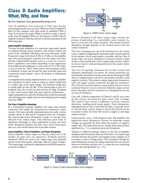
The output stage could also be implemented with MOS transistors,<br />
as shown in Figure 1.<br />
V IN<br />
MODULATOR<br />
SWITCHING<br />
OUTPUT<br />
STAGE<br />
OUTPUT<br />
STAGE<br />
6 <strong>Analog</strong> <strong>Dialogue</strong> <strong>Volume</strong> <strong>40</strong> Number 2<br />
V IN<br />
MH<br />
ML<br />
V DD<br />
V SS<br />
V OUT<br />
SPEAKER<br />
GROUND<br />
0V<br />
Figure 1. CMOS linear output stage.<br />
Power is dissipated in all linear output stages, because the<br />
process of generating V OUT unavoidably causes nonzero I DS<br />
and V DS in at least one output transistor. The amount of power<br />
dissipation strongly depends on the method used to bias the<br />
output transistors.<br />
The Class A topology uses one of the transistors as a dc current<br />
source, capable of supplying the maximum audio current required<br />
by the speaker. Good sound quality is possible with the Class A<br />
output stage, but power dissipation is excessive because a large<br />
dc bias current usually flows in the output-stage transistors (where<br />
we do not want it), without being delivered to the speaker (where<br />
we do want it).<br />
The Class B topology eliminates the dc bias current and<br />
dissipates significantly less power. Its output transistors are<br />
individually controlled in a push-pull manner, allowing the MH<br />
device to supply positive currents to the speaker, and ML to sink<br />
negative currents. This reduces output stage power dissipation,<br />
with only signal current conducted through the transistors.<br />
The Class B circuit has inferior sound quality, however, due to<br />
nonlinear behavior (crossover distortion) when the output current<br />
passes through 0 and the transistors are changing between the<br />
on and off conditions.<br />
Class AB, a hybrid compromise of Classes A and B, uses some<br />
dc bias current, but much less than a pure Class A design.<br />
The small dc bias current is sufficient to prevent crossover<br />
distortion, enabling good sound quality. Power dissipation,<br />
although between Class A and Class B limits, is typically closer<br />
to Class B. Some control, similar to that of the Class B circuit,<br />
is needed to allow the Class AB circuit to supply or sink large<br />
output currents.<br />
Unfortunately, even a well-designed class AB amplifier has<br />
significant power dissipation, because its midrange output<br />
voltages are generally far from either the positive or negative<br />
supply rails. The large drain-source voltage drops thus produce<br />
significant I DS 3 V DS instantaneous power dissipation.<br />
Thanks to a different topology (Figure 2), the Class D amplifier<br />
dissipates much less power than any of the above. Its output stage<br />
switches between the positive and negative power supplies so as<br />
to produce a train of voltage pulses. This waveform is benign for<br />
power dissipation, because the output transistors have zero current<br />
when not switching, and have low V DS when they are conducting<br />
current, thus giving smaller I DS 3 V DS.<br />
LOSSLESS<br />
LOW-PASS<br />
FILTER<br />
(LC)<br />
V OUT<br />
Figure 2. Class D open-loop-amplifier block diagram.<br />
SPEAKER