Smart Power IC-Entwicklung für die Automobiltechnik - HTL Wien 10
Smart Power IC-Entwicklung für die Automobiltechnik - HTL Wien 10
Smart Power IC-Entwicklung für die Automobiltechnik - HTL Wien 10

You also want an ePaper? Increase the reach of your titles
YUMPU automatically turns print PDFs into web optimized ePapers that Google loves.
Seminar<br />
Elektronik im KFZ<br />
Spital/Pyhrn 12/07<br />
Seite 1 H.Zitta / <strong>Smart</strong> <strong>Power</strong> <strong>IC</strong>-<strong>Entwicklung</strong><br />
Seminar<br />
Elektronik im KFZ<br />
Spital/Pyhrn 12/07<br />
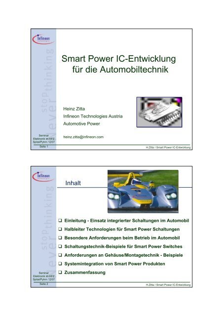
<strong>Smart</strong> <strong>Power</strong> <strong>IC</strong>- <strong>Entwicklung</strong><br />
<strong>für</strong> <strong>die</strong> <strong>Automobiltechnik</strong><br />
Heinz Zitta<br />
Infineon Technologies Austria<br />
Automotive <strong>Power</strong><br />
heinz.zitta@infineon.com<br />
Inhalt<br />
Einleitung - Einsatz integrierter Schaltungen im Automobil<br />
Halbleiter Technologien <strong>für</strong> <strong>Smart</strong> <strong>Power</strong> Schaltungen<br />
Besondere Anforderungen beim Betrieb im Automobil<br />
Schaltungstechnik-Beispiele <strong>für</strong> <strong>Smart</strong> <strong>Power</strong> Switches<br />
Anforderungen an Gehäuse/Montagetechnik - Beispiele<br />
Systemintegration von <strong>Smart</strong> <strong>Power</strong> Produkten<br />
Zusammenfassung<br />
Seite 2 H.Zitta / <strong>Smart</strong> <strong>Power</strong> <strong>IC</strong>-<strong>Entwicklung</strong><br />
• 1
Seite 3 H.Zitta / <strong>Smart</strong> <strong>Power</strong> <strong>IC</strong>-<strong>Entwicklung</strong><br />
Trends<br />
Automotive <strong>Power</strong> - Einsatzgebiete<br />
<strong>Power</strong>train – „Antriebsstrang“<br />
Safety<br />
o Motorsteuerung, Engine Management<br />
o Einspritzventile, Zü ndung<br />
o Getriebesteuerung<br />
o ABS, ASR, ESP (Elektron. Stabilitäts-Progr.)<br />
o Airbag<br />
„B o d y“ – Alles, was in der Karosserie ist<br />
o Lampenschalter (hoher „inrush-current “)<br />
o Fensterheber, Zentralverrieg. (T ü rmodul)<br />
o Relais, Signallampen, LED-Ansteuerung<br />
• Ersatz aller elektromechanischen durch elektronische Komponenten<br />
• “ Silicon instead of heatsink” Niedrige Rds- on sparen Verlustleistung<br />
• Verstärkter Einsatz von Bus- Systemen, Car - Communication<br />
• H öherer Komfort erhö ht prozentuellen Elektronik- Anteil im Auto<br />
• “ X by wire” Ersatz von Mechanik, Hydraulik durch Elektroantrieb<br />
• Ü bergang zu 42V Bordnetz? (war geplant, kommt wohl nicht mehr ...)<br />
• System on Chip<br />
• Selbsttest, Diagnosesysteme<br />
• Treibstoffverbrauchsreduktion (z.B. Benzin Direkteinspritzung)<br />
• Hohe Anforderung an Zuverlässigkeit f ür elektron. Komponenten<br />
• Abkehr von reinen kundenspezifischen Lös u n g e n :<br />
• Custom - specific<br />
• - > AS<strong>IC</strong> (Application Specific <strong>IC</strong>)<br />
• -> ASSP (Application Specific Standard Product)<br />
• - > Standard ?<br />
Seite 4 H.Zitta / <strong>Smart</strong> <strong>Power</strong> <strong>IC</strong>-<strong>Entwicklung</strong><br />
• 2
Seminar<br />
Elektronik im KFZ<br />
Spital/Pyhrn 12/07<br />
Einleitung - Einsatz integrierter Schaltungen im Automobil<br />
Halbleiter Technologien <strong>für</strong> <strong>Smart</strong> <strong>Power</strong> Schaltungen<br />
Besondere Anforderungen beim Betrieb im Automobil<br />
Schaltungstechnik-Beispiele f ü r <strong>Smart</strong> <strong>Power</strong> Switches<br />
Anforderungen an Gehä use/Montagetechnik - Beispiele<br />
Systemintegration von <strong>Smart</strong> <strong>Power</strong> Produkten<br />
Zusammenfassung<br />
Seite 5 H.Zitta / <strong>Smart</strong> <strong>Power</strong> <strong>IC</strong>-<strong>Entwicklung</strong><br />
Technologie Evolution: Shrinking Possibility Limited for <strong>Power</strong> Technologies<br />
W.Ziebert, „Technical and Economical Trends in Microelectronic “. ESSCIRC 2007. München<br />
Seite 6 H.Zitta / <strong>Smart</strong> <strong>Power</strong> <strong>IC</strong>-<strong>Entwicklung</strong><br />
• 3
ts 1<br />
n-substrate<br />
n-well<br />
ts 2<br />
p-substrat<br />
substrat<br />
<strong>Smart</strong> <strong>Power</strong> Technologien<br />
Klassifizierung entsprechend der angewandten Isolation:<br />
• Selbst-Isolation<br />
Diese Isolationstechnik ist von den CMOS Prozessen her bekannt. Es ist <strong>die</strong><br />
einfachste Art, benachbarte Bauteile werden nur durch Anlegen vo n<br />
S p a n n u n g e n e n t s p r e c h e n d e r P o l a r i t ä t im Vergleich zum Substratpotential oder<br />
v o m W a n n e n -Potential voneinander isoliert.<br />
<strong>Smart</strong> <strong>Power</strong> Selbstisolations Prozesse verwenden n-Substrat u. p-W a n n e n .<br />
• Sperrschicht Isolation (Junction -Isolation)<br />
Diese Art der Isolation ist von bipolaren Prozessen her bekannt. Auf ein p-<br />
Substrat wird eine n-dotierte Epischicht aufgebracht. Isolation der Bauteile<br />
innerhalb der Epischicht durch zusä tzliche, in Sperrschicht betriebene p-<br />
Diffusionen. Diese Art von <strong>Smart</strong> <strong>Power</strong> Prozessen benö tigt einen komplexeren<br />
Prozessaufbau (=hö her Maskenanzahl) als der Selbstisolations-Prozess, aber ist<br />
vielseitiger im Hinblick auf m ögliche Bauteile, einschließ l i c h b i p o l a r e r<br />
Komponenten. (Infineon: SPT, allgemein bekannt als BCD-P rozess)<br />
• Dielelektrische Isolation (SOI Silicon-o n -Insulator)<br />
E i n e „echte“ Isolation mittels Oxid.<br />
Beste Performance hinsichtlich Parasiten und Hochvolt -Festigkeit, jedoch am<br />
teuersten und daher derzeit nicht Mainstream f ü r automotive Produkte.<br />
Thermisches Verhalten: Si-Oxid ist ein deutlich schlechterer W ärmeleiter als Si.<br />
Seite 7 H.Zitta / <strong>Smart</strong> <strong>Power</strong> <strong>IC</strong>-<strong>Entwicklung</strong><br />
+Vdd<br />
n-well<br />
Self-Isolation<br />
device 1 device 2<br />
p p p p<br />
n- substrate<br />
It is the simplest solution and is used in each MOS process. Iso lation of<br />
neighbouring components is only done by applying the right voltages to the<br />
components in respect to the substrat or well connection. The sm art power self -<br />
isolation processes are based on a n-substrate/p-well CMOS approach.<br />
Apply a positive voltage to the n-substrate to allow isolation of p-type devices.<br />
Seite 8 H.Zitta / <strong>Smart</strong> <strong>Power</strong> <strong>IC</strong>-<strong>Entwicklung</strong><br />
• 4
Gnd (-)<br />
p<br />
iso<br />
p<br />
n- Epi<br />
Junction-Isolation<br />
device 1 device 2<br />
p - substrat<br />
p<br />
This kind of isolation is known from bipolar processes. A n-type epitaxial<br />
layer is grown on a p-type substrat. The components are inside the epi -<br />
layer and they are isolated by revers biased junctions realized by pdiffusions.<br />
This kind of smart power process needs a higher mask count as<br />
the self isolation approach, but is more flexible in the availab le devices.<br />
Substrate must be connected to GND or most negative voltage to<br />
enable the isolation.<br />
Seite 9 H.Zitta / <strong>Smart</strong> <strong>Power</strong> <strong>IC</strong>-<strong>Entwicklung</strong><br />
n<br />
p<br />
device 1 device 2<br />
substrat<br />
Seite <strong>10</strong> H.Zitta / <strong>Smart</strong> <strong>Power</strong> <strong>IC</strong>-<strong>Entwicklung</strong><br />
p<br />
Dielectric-Isolation<br />
p<br />
n<br />
n<br />
n<br />
n<br />
p<br />
oxid<br />
isolation<br />
This isolation is r e a l l y d o n e with an insulator (oxid ).<br />
It would give the best results in avoiding parasitics and f o r high voltage capability.<br />
For power circuits you would have to calculate, that the thermal conductivity o f<br />
oxid is v e r y l o w compared to silicon. Due to the fabrication process it is the m o s t<br />
expensive technology and therefore not (yet) the mainstream f o r smart power<br />
circuits.<br />
• 5
n<br />
p<br />
device 1 device 2<br />
p - substrate<br />
Partial Dielectric-Isolation<br />
Deep Trench Isolation (DTI)<br />
A oxid isolation o n l y to separate the n- wells is easier to realize than a f u l l <strong>die</strong>lectric<br />
isolation, it could be done with deep trench etching . The advantage is a smaller<br />
chip-size because o f less area wasted f o r the well- isolation compared to the<br />
junction-isolation.<br />
Against substrate there is no advantage related to parasitics („reverse current<br />
problem “)<br />
Seite 11 H.Zitta / <strong>Smart</strong> <strong>Power</strong> <strong>IC</strong>-<strong>Entwicklung</strong><br />
S G<br />
D<br />
Gate<br />
p- channel n- channel<br />
D r a i n<br />
Source<br />
S G<br />
D S G<br />
D<br />
B<br />
p +<br />
n- Epi<br />
n+ Substrat<br />
p-<br />
D<br />
n +<br />
G Bulk<br />
S<br />
p<br />
n<br />
n<br />
CMOS Self-Isolation<br />
oxid<br />
isolation<br />
Seite 12 H.Zitta / <strong>Smart</strong> <strong>Power</strong> <strong>IC</strong>-<strong>Entwicklung</strong><br />
+<br />
s u b s t r a t<br />
n- channel<br />
p- channel<br />
Correct biasing of all parasitic diodes<br />
is necessary to maintain self - isolation<br />
• 6
MOS: expand voltage capability<br />
low voltage<br />
MOS<br />
p- channel<br />
high voltage<br />
MOS<br />
S G<br />
D<br />
S G<br />
D<br />
S G<br />
D<br />
p + L p +<br />
L<br />
p + p-<br />
p +<br />
n<br />
Higher voltage capability requires longer channels for lateral M OS Devices<br />
- > increasing chip- area, increasing Rds- on<br />
introduce drain extension as a better solution:<br />
a h i g h- ohmic (low doped) diffusion of same type (n or p) as device typ ( n o r p - channel)<br />
increase gate- oxid thickness near drain (allow high drain- source voltage)<br />
Seite 13 H.Zitta / <strong>Smart</strong> <strong>Power</strong> <strong>IC</strong>-<strong>Entwicklung</strong><br />
LDD High Voltage Device: Electric Field<br />
VS=0V VG=+5V VD=+50V<br />
drain extension<br />
Lightly doped drain<br />
extension area<br />
reduces the electric<br />
field strength in the<br />
channel region.<br />
Also called“RESURF“<br />
device<br />
„reduced surface<br />
field“<br />
source:<br />
Balan, High voltage devices and<br />
circuits in standard CMOS<br />
technologies<br />
Seite 14 H.Zitta / <strong>Smart</strong> <strong>Power</strong> <strong>IC</strong>-<strong>Entwicklung</strong><br />
• 7
low voltage<br />
CMOS<br />
p- Kanal n- Kanal<br />
S<br />
G<br />
D<br />
B<br />
S G<br />
D<br />
p +<br />
CMOS: Low Voltage and High Voltage Devices<br />
can be on same chip<br />
p-<br />
n +<br />
n- Epi<br />
n+ Substrat<br />
p- Kanal<br />
S G<br />
D<br />
p + p-<br />
high voltage<br />
MOS<br />
Seite 15 H.Zitta / <strong>Smart</strong> <strong>Power</strong> <strong>IC</strong>-<strong>Entwicklung</strong><br />
p +<br />
n- Kanal<br />
S G<br />
D<br />
p-<br />
n + n-<br />
Insert a lightly doped drain diffusion for<br />
higher voltage capability (drain extension)<br />
• p- f o r P -channel device<br />
• n- f o r N -channel device Double diffusion MOS = DMOS<br />
(lateral DMOS)<br />
S<br />
p- n + p +<br />
n- epi<br />
n+ substrate<br />
G<br />
Current flow<br />
D r a i n<br />
Vertical DMOS<br />
Seite 16 H.Zitta / <strong>Smart</strong> <strong>Power</strong> <strong>IC</strong>-<strong>Entwicklung</strong><br />
n +<br />
Use the epi- l a y e r<br />
a s d r a i n e x t e n s i o n .<br />
The vertical DMOS is born!<br />
d Epi doping and thickness can be<br />
adjusted to the required<br />
breakdown voltage vs. Rds-on<br />
thumb- r u l e : d = 1 u m e a c h 1 0 V<br />
D r a i n = S u b s t r a t +<br />
Gate<br />
Source<br />
• 8
p +<br />
Gate<br />
low voltage<br />
CMOS<br />
p- Kanal n- Kanal<br />
p- Kanal<br />
n- Kanal<br />
S G<br />
D<br />
B<br />
S G<br />
D<br />
S G<br />
D<br />
S G<br />
D<br />
S<br />
G<br />
D r a i n<br />
Source<br />
Vertical SMART <strong>Power</strong> Technologie<br />
CMOSDMOS, SMART = Selfisolation<br />
n +<br />
p-<br />
n- Epi<br />
n+ Substrat<br />
D<br />
G Bulk<br />
S<br />
p + p-<br />
high voltage<br />
MOS<br />
p +<br />
p-<br />
n + n-<br />
Vertical D M O S<br />
<strong>Power</strong> Transistor<br />
+ Vbatt<br />
D r a i n<br />
D r a i n = S u b s t r a t +<br />
Seite 17 H.Zitta / <strong>Smart</strong> <strong>Power</strong> <strong>IC</strong>-<strong>Entwicklung</strong><br />
n +<br />
p- n + p +<br />
Gate<br />
Highside Switch: Vertical SMART Technology<br />
Source<br />
DMOS<br />
2 x 90 mOhm<br />
12 A / 60 V<br />
Analog MOS<br />
Diagnostic<br />
Protection<br />
Seite 18 H.Zitta / <strong>Smart</strong> <strong>Power</strong> <strong>IC</strong>-<strong>Entwicklung</strong><br />
• 9
p +<br />
n- epi- l a y e r<br />
p Substrat<br />
All components are in<br />
n- epi- w e l l s , i s o l a t e d b y<br />
p + i s o l a t i o n d i f f u s i o n s<br />
Bipolar Technology<br />
Junction Isolation<br />
Bipolar<br />
npn- T r a n s i s t o r<br />
C B<br />
E<br />
p +<br />
n +<br />
p<br />
n-<br />
n +<br />
p+<br />
Isolation s i n k e r<br />
buried l a y e r<br />
C B<br />
E<br />
pnp- T r a n s i s t o r ( l a t e r a l )<br />
B C E<br />
n- p p+<br />
C E<br />
Seite 19 H.Zitta / <strong>Smart</strong> <strong>Power</strong> <strong>IC</strong>-<strong>Entwicklung</strong><br />
B<br />
CMOS<br />
p- Kanal n- Kanal<br />
Bipolar<br />
npn- T r a n s i s t o r<br />
DMOS<br />
Vertical " U p d r a i n "<br />
<strong>Power</strong> Transistor<br />
S G<br />
D<br />
B<br />
S G<br />
D<br />
C<br />
B<br />
E D<br />
S<br />
G<br />
p +<br />
at GND level ( - )<br />
„Updrain“-<strong>Smart</strong> <strong>Power</strong> Technologie<br />
BIPOLARCMOSDMOS, SPT = Junction Isolation<br />
n +<br />
p Substrat<br />
p-<br />
n- Epi<br />
S<br />
p -K a n a l<br />
D<br />
D<br />
n -K a n a l<br />
S<br />
n +<br />
p<br />
p + n-<br />
n +<br />
p +<br />
Isolation s i n k e r<br />
buried l a y e r<br />
B<br />
Seite 20 H.Zitta / <strong>Smart</strong> <strong>Power</strong> <strong>IC</strong>-<strong>Entwicklung</strong><br />
C<br />
E<br />
B<br />
p- n + p +<br />
n +<br />
Drain: no restrictions<br />
Gate<br />
Source<br />
p +<br />
• <strong>10</strong>
Source: <strong>Smart</strong> <strong>Power</strong> Ics, Technologies and Applications, B. Murari et al (eds), Springer Verlag 1995, ISBN 3-540-60332-8<br />
Seite 21 H.Zitta / <strong>Smart</strong> <strong>Power</strong> <strong>IC</strong>-<strong>Entwicklung</strong><br />
current<br />
flow<br />
symbol<br />
DMOS Cross-section<br />
IGBT Insulated Gate Bipolar Transistor<br />
electrical<br />
subcircuit<br />
Isolation is done with two<br />
implantations:<br />
bottom isolation implanted<br />
before growing the<br />
epitaxial layer, top isolation<br />
implanted from surface<br />
included parasitics<br />
Seite 22 H.Zitta / <strong>Smart</strong> <strong>Power</strong> <strong>IC</strong>-<strong>Entwicklung</strong><br />
• 11
IGBT Insulated Gate Bipolar Transistor<br />
The IGBT combines the advantage of an easy to control MOS gate structure<br />
with the low conduction loss of a bipolar transistor.<br />
Although the symbol shows a npn-transistor, controlled by a gate, in reality it<br />
is better understood as a pnp-transistor, which base current is controlled by a<br />
n-channel MOS transistor. Therefore voltage drop in foreward direction is<br />
always higher than a bipolar diode.<br />
If we look at included parasitics we will find a thyristor structure, formed from<br />
npn and pnp device. Under normal operation conditions this thyristor is not<br />
activated.<br />
Resulting we can define the IGBT as a device between power-MOS and<br />
thyristor.<br />
The Non-Punch-Through (NPT) IGBT has a low doped n- region, designed to<br />
support the whole blocking voltage of the device. The Punch-Through (PT)<br />
concept uses an n+ -doped layer which seperates the active region of the<br />
device from the thick backside p+ emitter.<br />
A drawback of the IGBT is its lack of reverse blocking capabilit y (compared to<br />
bipolar) or the absence of a body diode (compared to MOS).<br />
Seite 23 H.Zitta / <strong>Smart</strong> <strong>Power</strong> <strong>IC</strong>-<strong>Entwicklung</strong><br />
Compare Characteristics: MOS-FET / IGBT<br />
SIPMOS BUZ 342<br />
V DS I D RDS( on)<br />
50 V 60 A 0,01 Ohm<br />
IGBT BUP 604<br />
V CE I C V CE( sat)<br />
600 V 80 A 2V (@50A)<br />
T j=25°C<br />
Seite 24 H.Zitta / <strong>Smart</strong> <strong>Power</strong> <strong>IC</strong>-<strong>Entwicklung</strong><br />
• 12
Seminar<br />
Elektronik im KFZ<br />
Spital/Pyhrn 12/07<br />
R on · A (W*mm 2 )<br />
Use the best suited technology for cost<br />
effective automotive power products<br />
discrete power transistor t o s y s t e m - i n t e g r a t i o n<br />
MOSFET<br />
/IGBT<br />
TEMPFET<br />
protected<br />
PROFET<br />
fully protected<br />
<strong>Smart</strong><br />
<strong>Power</strong> <strong>IC</strong>’s<br />
Multi-Channel Switches<br />
Bridges<br />
Driver-<strong>IC</strong>‘s<br />
Voltage Regulators<br />
<strong>Power</strong><br />
System <strong>IC</strong>’s<br />
<strong>Smart</strong> <strong>Power</strong><br />
System Integration:<br />
ABS / AIRBAG<br />
<strong>Power</strong>train<br />
Embedded<br />
<strong>Power</strong> Products<br />
single package<br />
smart power and<br />
controller integration<br />
low-side-Switch<br />
high-side-Switch<br />
Overload<br />
Integrated charge<br />
protection<br />
pump<br />
CCAN/LIN Transceiver<br />
Thermal shutdown<br />
Overload protectionDC/DC<br />
Converter<br />
Current limitation smart IGBT<br />
HITFET<br />
Short-circuit<br />
C u r r e n t limitation<br />
protection<br />
Short-circuit<br />
protection<br />
Overvoltage<br />
Overvoltage<br />
protection<br />
protection<br />
Open load detection<br />
O p e n load<br />
Diagnostic feedback<br />
detection<br />
Multi-Channel<br />
SFET/IGBT <strong>Smart</strong>&SFET <strong>Smart</strong> BIPOLAR, SPT,IGBT SPT / CMOS<br />
Seite 25 H.Zitta / <strong>Smart</strong> <strong>Power</strong> <strong>IC</strong>-<strong>Entwicklung</strong><br />
0,5<br />
0,4<br />
0,3<br />
0,2<br />
0,1<br />
0<br />
1990 1995 2000<br />
lithography<br />
R-on Reduction of <strong>Smart</strong> <strong>Power</strong> Technologies<br />
vertical updrain<br />
60 V<br />
90 V<br />
2.0 µm 1.2 µm<br />
0.5 µm<br />
0.35 µm<br />
Seite 26 H.Zitta / <strong>Smart</strong> <strong>Power</strong> <strong>IC</strong>-<strong>Entwicklung</strong><br />
2005<br />
• 13
Seite 27 H.Zitta / <strong>Smart</strong> <strong>Power</strong> <strong>IC</strong>-<strong>Entwicklung</strong><br />
P o w e r m e t a l<br />
(Aluminum)<br />
Source<br />
C h a n n e l<br />
Poly(Gate)<br />
from Lateral to Trench-DMOS<br />
p-<br />
for further R-on*Area reduction<br />
Lateral High-Voltage MOS<br />
S D<br />
n + n- n +<br />
lateral<br />
channel<br />
lateral<br />
drift region<br />
Vertical Trench DMOS<br />
<strong>Power</strong>-Transistor in Trench-Technik<br />
Drain<br />
S<br />
D<br />
G<br />
vertical<br />
channel<br />
vertical<br />
drift region<br />
Seite 28 H.Zitta / <strong>Smart</strong> <strong>Power</strong> <strong>IC</strong>-<strong>Entwicklung</strong><br />
• 14
Self - Isolation<br />
Vertical <strong>Smart</strong><br />
Junction Isolation<br />
BCD, SPT<br />
Possible <strong>Power</strong> Output Configurations<br />
With Integrated <strong>Power</strong> Technologies<br />
High-Side<br />
Switch<br />
+ V s<br />
++<br />
Low-Side<br />
Switch<br />
1 channel +<br />
multi- ch. -<br />
Half-<br />
Bridge<br />
H - Bridge<br />
+ ++ +<br />
+<br />
Seite 29 H.Zitta / <strong>Smart</strong> <strong>Power</strong> <strong>IC</strong>-<strong>Entwicklung</strong><br />
Four-f old smart power low-side switch in SPT-T e c h n o l o g y<br />
rated max. 3 A , 60 V each channel<br />
Analog:<br />
Driver,<br />
diagnostic and<br />
Protection<br />
DMOS<br />
It consists of the power DMOS, logic CMOS circuits and analog circuit<br />
realized in SPT-Technology (TLE 6220)<br />
Seite 30 H.Zitta / <strong>Smart</strong> <strong>Power</strong> <strong>IC</strong>-<strong>Entwicklung</strong><br />
CMOS Logic<br />
-<br />
-<br />
• 15
Seminar<br />
Elektronik im KFZ<br />
Spital/Pyhrn 12/07<br />
Einleitung - Einsatz integrierter Schaltungen im Automobil<br />
Halbleiter Technologien f ü r <strong>Smart</strong> <strong>Power</strong> Schaltungen<br />
Besondere Anforderungen beim Betrieb im Automobil<br />
Schaltungstechnik-Beispiele f ü r <strong>Smart</strong> <strong>Power</strong> Switches<br />
Anforderungen an Gehä use/Montagetechnik - Beispiele<br />
Systemintegration von <strong>Smart</strong> <strong>Power</strong> Produkten<br />
Zusammenfassung<br />
Seite 31 H.Zitta / <strong>Smart</strong> <strong>Power</strong> <strong>IC</strong>-<strong>Entwicklung</strong><br />
Besondere Anforderungen beim Betrieb im Automobil<br />
• Hoher Spannungsbereich 5V .. 60 V (90V)<br />
• Hoher Temperaturbereich<br />
• - 40 °C .. + 150 °C voll getestet, jedes Device<br />
• 150 °C .. + 200 °C volle Funktion<br />
• > 200°C bis 300°C bei Überlast, kontrolliertes Abschalten<br />
• St ö runempfindlichkeit<br />
• Übersprechen (Kabelbä u m e )<br />
• EMV Einstrahlung (Susceptibility)<br />
• EMV Abstrahlung (Emission)<br />
• Hohe Qualitätsanforderungen<br />
• Zuverlä ssigkeit (Engine-Management)<br />
• Sicherheitsrelevanz (ABS, Airbag)<br />
Seite 32 H.Zitta / <strong>Smart</strong> <strong>Power</strong> <strong>IC</strong>-<strong>Entwicklung</strong><br />
• 16
Operating voltages in automotive applications ...<br />
42V <strong>Power</strong> Net<br />
12V 5<br />
7 18<br />
18<br />
30 nominal voltage 50<br />
12 24 36 48 60<br />
42<br />
Coresponding<br />
Wafer technology limit<br />
Seite 33 H.Zitta / <strong>Smart</strong> <strong>Power</strong> <strong>IC</strong>-<strong>Entwicklung</strong><br />
58<br />
60 75<br />
75<br />
75 90<br />
… is against the trend of downsizing micro-controller core voltages<br />
‡0,5µm
V<br />
12V<br />
-<strong>10</strong>0V<br />
Negative Voltage Transients can cause Reverse Current<br />
<strong>10</strong>%<br />
90%<br />
200ms<br />
Seminar<br />
Elektronik im KFZ<br />
Spital/Pyhrn 12/07<br />
Seite 37 H.Zitta / <strong>Smart</strong> <strong>Power</strong> <strong>IC</strong>-<strong>Entwicklung</strong><br />
Vbat<br />
+ 12 .. 60V<br />
Logic<br />
IN<br />
Logic<br />
OUT<br />
V C C<br />
+ 5 V<br />
Einleitung - Einsatz integrierter Schaltungen im Automobil<br />
Halbleiter Technologien f ü r <strong>Smart</strong> <strong>Power</strong> Schaltungen<br />
Besondere Anforderungen beim Betrieb im Automobil<br />
Schaltungstechnik-Beispiele <strong>für</strong> <strong>Smart</strong> <strong>Power</strong> Switches<br />
Anforderungen an Gehä use/Montagetechnik - Beispiele<br />
Systemintegration von <strong>Smart</strong> <strong>Power</strong> Produkten<br />
Zusammenfassung<br />
R 1<br />
R 2<br />
I1<br />
<strong>IC</strong><br />
Q1<br />
I2<br />
M1 M2<br />
Block diagram of a <strong>Smart</strong> <strong>Power</strong> Switch<br />
Prestabilisation<br />
Voltage Regulator<br />
I/O Buf<br />
Digital<br />
Logic<br />
Parallel/<br />
Seriell<br />
Interface<br />
S P I<br />
C A N -Bus<br />
. . . . .<br />
Reference-Voltage<br />
& B i a s -Current<br />
Generation<br />
Internal S u p p l y<br />
Vref1<br />
Vref1<br />
Iref1<br />
Iref1<br />
Diagnostic & Protection<br />
Overlaod<br />
Overcurrent<br />
Overtemperature<br />
Open Load<br />
Gate Driver<br />
Slewrate -<br />
Control<br />
Seite 38 H.Zitta / <strong>Smart</strong> <strong>Power</strong> <strong>IC</strong>-<strong>Entwicklung</strong><br />
M3<br />
<strong>Power</strong><br />
DMOS<br />
• 19
Seminar<br />
Elektronik im KFZ<br />
Spital/Pyhrn 12/07<br />
Examples of Analog <strong>Smart</strong> <strong>Power</strong> Circuit Blocks<br />
Reference Voltage & Current Generation<br />
Bipolar transistor characteristic<br />
Bandgap reference circuit<br />
Diagnostic & Protection Circuits<br />
Temperature sensors<br />
Current measurement<br />
Overvoltage protection<br />
Open load detection<br />
Gate Driver & Slew-rate Control<br />
Low side<br />
High side<br />
Seite 39 H.Zitta / <strong>Smart</strong> <strong>Power</strong> <strong>IC</strong>-<strong>Entwicklung</strong><br />
Voltage Reference: Bandgap Circuits<br />
Vref<br />
Seite 40 H.Zitta / <strong>Smart</strong> <strong>Power</strong> <strong>IC</strong>-<strong>Entwicklung</strong><br />
• 20
What characteristic can be used to generate a reference voltage?<br />
Vbe<br />
Bipolar MOS<br />
Base-emitter-voltage Vbe:<br />
depends on temperature, but is not<br />
sensitive to process variation.<br />
Bipolar device is the key<br />
component for accurate<br />
voltage reference circuits<br />
Vgs<br />
Gate-source-voltage Vgs:<br />
Depends strong on process variation<br />
MOS device based voltage<br />
reference circuits will not<br />
achieve high accuracy<br />
Seite 41 H.Zitta / <strong>Smart</strong> <strong>Power</strong> <strong>IC</strong>-<strong>Entwicklung</strong><br />
I C<br />
1 mA<br />
<strong>10</strong>0 µ A<br />
Characteristic of bipolar transistor Ic = f (Vbe)<br />
0 , 2 0 , 4 0 , 6<br />
0 , 8<br />
I<br />
C<br />
V BE ⎛ ⎞<br />
⎜ Vt = I ⋅ ⎟<br />
S ⎜<br />
e −1<br />
⎟<br />
⎝ ⎠<br />
log(I C)<br />
linear scale logarithmic scale<br />
1 mA<br />
<strong>10</strong>0 µ A<br />
U BE [V]<br />
<strong>10</strong> µ A<br />
1 µ A<br />
I S<br />
k T<br />
Vt = mV C<br />
q<br />
⋅<br />
≈ 26 [ 25°<br />
]<br />
0 , 2 0 , 4 0 , 6<br />
0 , 8<br />
U BE [V]<br />
Seite 42 H.Zitta / <strong>Smart</strong> <strong>Power</strong> <strong>IC</strong>-<strong>Entwicklung</strong><br />
• 21
U BE<br />
1,2<br />
1,0<br />
0,8<br />
0,6<br />
0,4<br />
0,2<br />
extended temp.range<br />
Bipolar Transistor: V BE = f (T)<br />
Temperature behaviour approx. - 2mV/K<br />
<strong>IC</strong>=<strong>10</strong>0µA<br />
<strong>IC</strong>=<strong>10</strong>µ A<br />
0 K<br />
- 273 C<br />
300 K 400 K<br />
Normal operating range for integrated circuits<br />
in a u t o m o t i v e applications<br />
-40 C 27 C<br />
150 175C<br />
Seite 43 H.Zitta / <strong>Smart</strong> <strong>Power</strong> <strong>IC</strong>-<strong>Entwicklung</strong><br />
log(Ic)<br />
1 mA<br />
<strong>10</strong>0 µ A<br />
<strong>10</strong> µ A<br />
1 µ A<br />
I S<br />
Calculation of Delta- Vbe<br />
0 , 2 0 , 4 0 , 6<br />
0 , 8<br />
Ic1<br />
Ic2<br />
ΔVBE<br />
U BE [V]<br />
absolute value of Vbe depends on transistor parameter Is,<br />
delta Vbe is independent of individual transistor parameter<br />
V BE ⎛ ⎞<br />
⎜ Vt = I ⋅ ⎟<br />
S ⎜<br />
e −1<br />
⎟<br />
⎝ ⎠<br />
Seite 44 H.Zitta / <strong>Smart</strong> <strong>Power</strong> <strong>IC</strong>-<strong>Entwicklung</strong><br />
I<br />
V<br />
C<br />
BE<br />
ΔV<br />
⎛ I<br />
= ln<br />
⎜<br />
⎝ I<br />
BE<br />
C<br />
S<br />
⎛ I<br />
= ln<br />
⎜<br />
⎝ I<br />
⎞<br />
⎟ ⋅Vt<br />
⎠<br />
C 1<br />
C 2<br />
⎞<br />
⎟ ⋅Vt<br />
⎠<br />
T<br />
k T<br />
Vt = mV C<br />
q<br />
⋅<br />
≈ 26 [ 25°<br />
]<br />
−23<br />
k = 1, 38⋅<strong>10</strong> J/ K<br />
−19<br />
q = 1, 602⋅<strong>10</strong> As<br />
T [ ° C ] T [ K ] VT [mV]<br />
- 4 0 2 3 3 20,1<br />
2 5 2 9 8 25,7<br />
1 0 0 3 7 3 32,1<br />
1 5 0 4 2 3 36,4<br />
2 0 0 4 7 3 40,7<br />
• 22
V REF<br />
Temperature- compensation of Vbe voltage<br />
Vbe<br />
Δ Vbe<br />
T<br />
T<br />
25 C 150 C<br />
Seite 45 H.Zitta / <strong>Smart</strong> <strong>Power</strong> <strong>IC</strong>-<strong>Entwicklung</strong><br />
-40 C<br />
Vref = const.<br />
The negative temperature dependence of Vbe can be compensated<br />
by the positive temperature dependence of delta-Vbe<br />
V BE2<br />
V BE1<br />
V R1<br />
V R2<br />
Temperature-constant Reference Voltage<br />
“B andgap-Reference”<br />
Q1<br />
n : 1 Q2<br />
R1<br />
R2<br />
+Vdd<br />
Q3 Q4<br />
I1 I2 C1<br />
Q5<br />
R3<br />
R4<br />
Seite 46 H.Zitta / <strong>Smart</strong> <strong>Power</strong> <strong>IC</strong>-<strong>Entwicklung</strong><br />
V REF<br />
1,2<br />
0,6<br />
Vbe<br />
Δ Vbe<br />
V REF<br />
-40 C<br />
25 C<br />
T<br />
Vbe<br />
Δ<br />
V BE2<br />
V R2<br />
Vbe<br />
125 C<br />
T<br />
T<br />
T<br />
• 23
Calculation of b a n d g a p reference circuit<br />
Assumption: I1 =I2, this i s done b y current mirror Q3,Q4.<br />
Q1, Q2 have different emitter areas (AE) with AE(Q1) > AE(Q2) .<br />
Ratio n i s choosen as integer.<br />
If collector-currents are equal , the base-emitter-voltages (V BE) of Q1, Q2 are different.<br />
Δ<br />
V BE<br />
= Vt ⋅ ln<br />
V R 1 = Δ V BE<br />
( n )<br />
=<br />
I<br />
1<br />
⋅ R<br />
1<br />
AE( Q1)<br />
n =<br />
AE( Q2)<br />
k<br />
Vt<br />
q T = ⋅<br />
R 2<br />
V R 2 = ( I 1 + I 2 ) ⋅ R 2 = 2 ⋅ I 1 ⋅ R 2 = 2 ⋅ ⋅ Δ V<br />
R<br />
VREF = VBE<br />
2 + VR<br />
2<br />
= 1,<br />
20...<br />
1,<br />
25V<br />
Example:<br />
n=<strong>10</strong><br />
Δ V BE = 60 mV [ 25 C ]<br />
R2/R1 = 5<br />
V R 2 = 6 0 0 m V<br />
VBE2=600 m V<br />
V R E F = 1,2 V<br />
Voltage drop at R1 equals delta -V b e and has the s a m e positiv tc (temp.coefficient) as V t. So<br />
a l s o the voltage VR2 has the s a m e tc, the absolute value of V R 2 i s choosen to a value similar<br />
to V B E .<br />
T h i s leads to a compensation of the negative tc o f V B E over full temperature range. The<br />
resulting temperature error i s of 2nd order and i s i n practice lower than 1%. The best<br />
temperature compensation will be achieved if the voltage Vref i s adjusted to 1.2 - 1.25 V. The<br />
absolute value o f this reference voltage i s better than + /- 5% assuming all practical<br />
manufacturing tolerances<br />
Seite 47 H.Zitta / <strong>Smart</strong> <strong>Power</strong> <strong>IC</strong>-<strong>Entwicklung</strong><br />
Ibias<br />
1<br />
for optimal<br />
BE<br />
temp.<br />
comp.<br />
Bandgap<br />
Reference<br />
Circuit<br />
Practical example of a<br />
circuit realized in a<br />
SPT (BCD)<br />
technology<br />
Seite 48 H.Zitta / <strong>Smart</strong> <strong>Power</strong> <strong>IC</strong>-<strong>Entwicklung</strong><br />
• 24
Startup- Problem of Bandgap- Reference Circuit<br />
I1 I2 C1<br />
Q5<br />
R3<br />
I1 I2<br />
Vref<br />
Q1<br />
n : 1 Q2<br />
R1<br />
R2<br />
+Vdd<br />
Q3 Q4<br />
R4<br />
V REF<br />
Seite 49 H.Zitta / <strong>Smart</strong> <strong>Power</strong> <strong>IC</strong>-<strong>Entwicklung</strong><br />
R1<br />
R2<br />
I2 I1<br />
V BG<br />
Current Mirror Q3/Q4 forces I1=I1,<br />
this defines the operating point.<br />
But there exists a second stable<br />
operating point: I1=I2=0<br />
A startup- circuit is required<br />
Adjustment of bandgap reference voltage<br />
Vref<br />
V r e f<br />
- 40°C - 25°C 150°C<br />
Adjusting the Vref by changing the value of the resistor ratio R1/R2 changes not only the<br />
output voltage but also the temperature behaviour.<br />
There exists one point with minimal temperature depedence (in pr actice < 1%)<br />
For bipolar technologies this optimal voltage is around 1,25V<br />
Adjustement can be done during wafer measurement, using „ zener - zapping“ or laser<br />
trimming.<br />
Seite 50 H.Zitta / <strong>Smart</strong> <strong>Power</strong> <strong>IC</strong>-<strong>Entwicklung</strong><br />
T<br />
• 25
Accuracy of voltage dividers (diffusion resistors)<br />
V1<br />
a) b)<br />
R 1<br />
R 2<br />
V2<br />
well connection<br />
V2/V1<br />
Seite 51 H.Zitta / <strong>Smart</strong> <strong>Power</strong> <strong>IC</strong>-<strong>Entwicklung</strong><br />
k<br />
k =<br />
R2<br />
R + R )<br />
( 1 2<br />
a) all resistors in one well – not suited for precision resistor divider<br />
b) each resistor in separate well – better accuracy<br />
Remark: this problem does not exist for polysilicon resistors<br />
Diffusion Resistor Voltage Divider - Layout<br />
R 1 R 2<br />
pp-<br />
p resistor<br />
n- well<br />
resistor p<br />
p<br />
presistor<br />
n- well<br />
p<br />
presistor<br />
n- well<br />
Seite 52 H.Zitta / <strong>Smart</strong> <strong>Power</strong> <strong>IC</strong>-<strong>Entwicklung</strong><br />
p<br />
V1<br />
a<br />
b<br />
a)<br />
all resistors in one well:<br />
R2 sees a higher voltage in<br />
respect to the n- well -> t e n d s<br />
to be highohmic compared to<br />
R1, caused by the backgate<br />
effect.<br />
b)<br />
each transistor<br />
in separate wells:<br />
better for accurate<br />
matching<br />
• 26
CMOS Compatible Bandgap Reference<br />
If in a CMOS process no real npn is available, u s e t h e „ substrat- npn“ , which always<br />
is available in a p- well CMOS technology, as bipolar reference .<br />
e.g . i n the <strong>Smart</strong> technology this s u b s t r a t- npn exists.<br />
The collector is f i x e d t o + Vbat ( = substrat in that technologies), so you cannot u s e<br />
the npn as amplifier . You h a v e only free access to base and emitter , which is enough<br />
to use the emitter - scaling for t h e D e l t a- Vbe principle.<br />
Amplifier has t o b e d o n e in MOS which will cause m o r e offset as a pure bipolar<br />
solution .<br />
p- Kanal n- Kanal<br />
npn<br />
S G<br />
D<br />
B<br />
S G<br />
D<br />
E<br />
B<br />
+Vbat = Substrat<br />
p +<br />
n +<br />
p-<br />
CMOS p- well process<br />
e.g . logic p a r t of <strong>Smart</strong><br />
n Substrat<br />
C<br />
Seite 53 H.Zitta / <strong>Smart</strong> <strong>Power</strong> <strong>IC</strong>-<strong>Entwicklung</strong><br />
Bandgap reference with all npn-collectors connected to VDD<br />
+Vdd = Substrat (for p- well CMOS)<br />
Seite 54 H.Zitta / <strong>Smart</strong> <strong>Power</strong> <strong>IC</strong>-<strong>Entwicklung</strong><br />
Vref<br />
B<br />
M O S O p a m p<br />
1) This is a possibility solution to realize a bandgap reference in a CMOS<br />
technology<br />
take care of opamp offset<br />
2) This circuit is robust against leakage currents and other parasitic currents at the<br />
bipolar collectors. So it can also be used with bipolars in the BCD process to<br />
improve robustness.<br />
C<br />
E<br />
• 27
M 1 M 2<br />
1 : m<br />
I1 I2 I3<br />
Q2<br />
R3<br />
n : 1<br />
Current - Reference<br />
based on Delta -Vbe<br />
Q1<br />
M 3<br />
I f M 1 = M 2 -> I1 = I2<br />
ΔVBE<br />
Vt ⋅ln(<br />
n)<br />
I1 = =<br />
R R1<br />
Seite 55 H.Zitta / <strong>Smart</strong> <strong>Power</strong> <strong>IC</strong>-<strong>Entwicklung</strong><br />
1<br />
If M1, M2 not equal: M2/M1 = m<br />
Ratio m acts as multiplication-factor:<br />
ΔV<br />
BE Vt ⋅ ln( n ⋅ m )<br />
I 1 = =<br />
R R1<br />
1<br />
Temperature behaviour:<br />
A resistor R3 with positive temp.coefficient (e.g. diffusion resistor)<br />
would give a temperature compensation of ΔVBE<br />
Diagnostic and Protection of <strong>Smart</strong> <strong>Power</strong> Switches<br />
o n<br />
status<br />
reset<br />
feedback<br />
- loop<br />
Overcurrent<br />
Overtemperature<br />
Overvoltage<br />
Open Load<br />
measure<br />
switch - o f f<br />
latch<br />
This is really the „<strong>Smart</strong>“ part of <strong>Smart</strong> <strong>Power</strong> devices<br />
Seite 56 H.Zitta / <strong>Smart</strong> <strong>Power</strong> <strong>IC</strong>-<strong>Entwicklung</strong><br />
logic<br />
• 28
C<br />
200<br />
150<br />
<strong>10</strong>0<br />
50<br />
K<br />
450<br />
400<br />
350<br />
300<br />
Temperature Sensors<br />
Leakage current detection<br />
Bipolar VBE monitoring<br />
Robustness aginst epi- well parasitics<br />
Position of temperature sensor in layout<br />
Seite 57 H.Zitta / <strong>Smart</strong> <strong>Power</strong> <strong>IC</strong>-<strong>Entwicklung</strong><br />
Temperature Sensor (1)<br />
Using t h e leakage current as temperature signal<br />
R 1<br />
I C B<br />
V+<br />
I1<br />
V TMP<br />
Leakage current is very low at junction temperatures < 150°C. For higher temperatures it<br />
increases exponentially, doubling approx. for each <strong>10</strong>K of temper ature increase. Therefore<br />
the leakage current is a good indicator to detect an overtemperature in the range > 150°C in<br />
integrated smart power circuits. In a MOS technology the always available parasitic substrat<br />
npn can be used as bipolar device. The temperature threshold is only in a given range<br />
adjustable by the values of R1 and I1, the exact temperature is not predictable (in contrast to<br />
direct Vbe measurement)<br />
Seite 58 H.Zitta / <strong>Smart</strong> <strong>Power</strong> <strong>IC</strong>-<strong>Entwicklung</strong><br />
I C B<br />
V TMP<br />
150 °C<br />
T<br />
T<br />
• 29
Temperature Sensor Circuit ( 2 )<br />
C o m p a r i n g of the bipolar VBE voltage with a stable reference<br />
R 1<br />
R 2<br />
I1<br />
<strong>IC</strong><br />
Q1<br />
I2<br />
M 1 M 2<br />
M 3<br />
V TMP<br />
V TMP<br />
Seite 59 H.Zitta / <strong>Smart</strong> <strong>Power</strong> <strong>IC</strong>-<strong>Entwicklung</strong><br />
U B E<br />
V R E F<br />
<strong>IC</strong>=I1+I2<br />
<strong>IC</strong>=I1<br />
Bipolar Bipolar characteristic of of approx. -2mV/K -2mV/K of of Vbe Vbe is is very very reliable<br />
reliable<br />
Hysterese<br />
Temperature Sensor with npn- Collector at VCC<br />
more robust against parasitics of bipolar collector (epi- well)<br />
Epi well (C of npn) is often affected by<br />
parasitics<br />
( reverse current, EMC,<br />
high temperature leakage currents ...)<br />
VCC<br />
Seite 60 H.Zitta / <strong>Smart</strong> <strong>Power</strong> <strong>IC</strong>-<strong>Entwicklung</strong><br />
Vref<br />
Solution:<br />
T e m p -sensor with with npn-C at at supply line,<br />
line,<br />
emitter as as temp-information<br />
T<br />
T<br />
Hysteresis<br />
• 30
Temperature Sensor w i t h D e l a y<br />
Example of realised circuit<br />
temp-sensor comparator current-mirror<br />
delay logic-o u t<br />
Seite 61 H.Zitta / <strong>Smart</strong> <strong>Power</strong> <strong>IC</strong>-<strong>Entwicklung</strong><br />
D<br />
Positioning of Temperature Sensor in Layout<br />
B<br />
<strong>Power</strong>-DMOS<br />
A<br />
C<br />
E<br />
Where is the best position?<br />
A center<br />
B inside, but not center<br />
C outside, at long edge<br />
D outside, at short edge<br />
E outside, chiptemp.<br />
Use thermal simulation to define the temp.sensor threshold of the sensor<br />
to ensure protection in case of short circuit with max. power dis sipation<br />
Seite 62 H.Zitta / <strong>Smart</strong> <strong>Power</strong> <strong>IC</strong>-<strong>Entwicklung</strong><br />
• 31
Seite 63 H.Zitta / <strong>Smart</strong> <strong>Power</strong> <strong>IC</strong>-<strong>Entwicklung</strong><br />
3 0 0 µs<br />
Thermal Simulation<br />
Ch 3 Ch 6<br />
Ch 4<br />
Treiber Treiber Treiber<br />
Treiber Treiber Treiber<br />
Dynamic Thermal FEM Simulation<br />
1ms<br />
3ms<br />
Ch 5<br />
Heat source<br />
(junction)<br />
<strong>10</strong>ms<br />
Logik<br />
Ch 2<br />
Ch 1<br />
To decide size<br />
of power-DMOS<br />
(if not only<br />
R-on related)<br />
and best position<br />
of temperature<br />
sensors<br />
Chip cross section<br />
(through DMOS)<br />
Seite 64 H.Zitta / <strong>Smart</strong> <strong>Power</strong> <strong>IC</strong>-<strong>Entwicklung</strong><br />
• 32
Verifying of the the<br />
thermal model by<br />
i n f r a r e d t h e r m o g r a f y<br />
Seite 65 H.Zitta / <strong>Smart</strong> <strong>Power</strong> <strong>IC</strong>-<strong>Entwicklung</strong><br />
Seminar<br />
Elektronik im KFZ<br />
Spital/Pyhrn 12/07<br />
4<br />
K / W<br />
3<br />
2<br />
1<br />
T h e r m o g r a f i e ( 3 0 W , 1 4 7 ° C )<br />
F E M ( 4 . 5 W , 1 4 1 ° C )<br />
• Diagnostic & Protection Circuits<br />
– Temperature Sensors<br />
– Current Measurement<br />
– Overvoltage Protection<br />
– Openload Detection<br />
0<br />
- 2 - 1 0 1 mm<br />
2<br />
Seite 66 H.Zitta / <strong>Smart</strong> <strong>Power</strong> <strong>IC</strong>-<strong>Entwicklung</strong><br />
• 33
R1<br />
Current Measurement with Shunt- Resistor<br />
I LAST<br />
V 1<br />
V REF<br />
+<br />
-<br />
I OVL<br />
Requires a reference v o l t a g e<br />
I LAST<br />
V REF<br />
Seite 67 H.Zitta / <strong>Smart</strong> <strong>Power</strong> <strong>IC</strong>-<strong>Entwicklung</strong><br />
R1<br />
V 1<br />
I OVL<br />
Current Measurement with Shunt- Resistor<br />
Comparator uses Delta -V B E principle<br />
I LAST<br />
U R1<br />
I 1 I 2<br />
Q1 Q2 n : 1<br />
n = ratio of emitter areas Q1/Q2<br />
I OVL<br />
R1 a s aluminum -resistor results in a good first order temperature compensation of Vt (TK AL = 3,8 <strong>10</strong> - 3 )<br />
Seite 68 H.Zitta / <strong>Smart</strong> <strong>Power</strong> <strong>IC</strong>-<strong>Entwicklung</strong><br />
I LAST<br />
U R1<br />
U S<br />
U IOVL<br />
Calculation of threshold U S :<br />
U V n I2<br />
S = t ⋅ln( ⋅ )<br />
I1<br />
z.B. I1 = I2 , n=2 U S = 18 mV bei 25C<br />
• 34
Current Measurement with Sense- Transistor<br />
Shunt -resistance in series to sense -cell<br />
I LAST<br />
I SENS<br />
M1 z : 1<br />
M2<br />
R1 U R1<br />
I 1 I 2<br />
Q1 Q2 n : 1<br />
Seite 69 H.Zitta / <strong>Smart</strong> <strong>Power</strong> <strong>IC</strong>-<strong>Entwicklung</strong><br />
I OVL<br />
U<br />
R1<br />
1 R<br />
I LAST = ⋅<br />
z +<br />
The layout of the powerdevice (DMOS) in general consist of many cells (> <strong>10</strong>00). One or few<br />
cells are used as sense cells, the current ratio between main (M1) and sense DMOS (M2) is<br />
defined by the ratio z. The shunt resistor R1 must therefore not be dimensioned for the full load<br />
current and, as additional advantage, the shunt resistor does not generate a voltage drop in<br />
series to the power DMOS.<br />
M1<br />
Current Measurement with Sense- Transistor<br />
without Shunt -Resistor<br />
I LAST<br />
z : 1<br />
M2<br />
I REF<br />
VP<br />
I OVL<br />
VN VN<br />
VP = RdsOn( M1) ⋅ I LAST<br />
Here the voltage drop at the power-transistor itself is used as current measuring device. This<br />
allows the measurement of high currents (overload) and very low currents (open load<br />
detection), depending on the choosen value of the reference current.<br />
Seite 70 H.Zitta / <strong>Smart</strong> <strong>Power</strong> <strong>IC</strong>-<strong>Entwicklung</strong><br />
I LAST<br />
VP<br />
I OVL<br />
VP = RdsOn ( M 2)<br />
⋅ I REF<br />
RdsOn( M 2 ) = z ⋅<br />
RdsOn( M 1)<br />
1<br />
• 35
+ Vbat<br />
D<br />
M1 M2<br />
z : 1<br />
S<br />
I Load<br />
S- sense<br />
OUT<br />
RLoad Rs<br />
(x Ampere) ( x m A )<br />
I FB<br />
CFB<br />
M3<br />
ON<br />
A / D<br />
µ C<br />
Current Feedback<br />
With sense-cells a given ratio of<br />
the load current can be mirrored<br />
to a pin as current feedback<br />
signal. To obtain the same drain<br />
voltage at the sense-DMOS as of<br />
the power-DMOS the gate<br />
voltage of an additional Transistor<br />
M3 in series to the sens DMOS<br />
M2 is controlled by a regulationloop.<br />
Current can than be acurate<br />
measured in application by using<br />
the A/D port of a µC<br />
Note: For a vertical technology (Highside<br />
Switch) the Sens Ratio of DMOS cells is<br />
very accurate, for updrain DMOS (BCD) the<br />
ratio of few cells to a large DMOS is not so<br />
good defined. That, and also offset of<br />
opamp can limit accuracy to approx. <strong>10</strong>% .<br />
Seite 71 H.Zitta / <strong>Smart</strong> <strong>Power</strong> <strong>IC</strong>-<strong>Entwicklung</strong><br />
Seminar<br />
Elektronik im KFZ<br />
Spital/Pyhrn 12/07<br />
• Diagnostic & Protection<br />
Circuits<br />
– Temperature Sensors<br />
– Current Measurement<br />
– Overvoltage Protection<br />
– Openload Detection<br />
Seite 72 H.Zitta / <strong>Smart</strong> <strong>Power</strong> <strong>IC</strong>-<strong>Entwicklung</strong><br />
• 36
Freewheeling diode<br />
disadvantage:<br />
switch off delay<br />
Circuit measures against overvoltages<br />
caused by switching inductances<br />
Clamping with<br />
external voltage<br />
<strong>Power</strong> transistor is<br />
switched on at high<br />
voltages - limits voltage<br />
like a power Z-diode<br />
Seite 73 H.Zitta / <strong>Smart</strong> <strong>Power</strong> <strong>IC</strong>-<strong>Entwicklung</strong><br />
Overvoltage protection - Switching of inductive loads<br />
Integrating the Z-diode into the smart power device<br />
U IN<br />
I O U T<br />
U O U T<br />
U S T<br />
t o n<br />
I OpenLoad<br />
t A Z<br />
Current Imax at switch-off depends on turn-o n t i m e .<br />
i f t o n > > t i m e-constant L/R than imax is only defined<br />
by ohmic resistor R of coil<br />
I m a x<br />
Seite 74 H.Zitta / <strong>Smart</strong> <strong>Power</strong> <strong>IC</strong>-<strong>Entwicklung</strong><br />
U Z<br />
V S<br />
T i m e t AZ can be calculated from amount of<br />
energy which is stored in the inductance.<br />
E m<br />
L I<br />
=<br />
Set magnetic energy equal to electrical<br />
energy:<br />
2<br />
⋅ max<br />
2<br />
⎛<br />
I = I ⋅ ⎜ − e<br />
⎝<br />
IN<br />
∫<br />
( )<br />
E = I ⋅ U − V ⋅ dt<br />
el out z s<br />
⎞<br />
⎠<br />
Vz<br />
V<br />
R<br />
R+L<br />
Vs<br />
t<br />
−<br />
τ<br />
max 1 ⎟<br />
τ = L<br />
S<br />
I max =<br />
R<br />
I OUT<br />
• 37
Clamping with slew rate controlled soft clipping<br />
Reference<br />
Voltage<br />
Vref<br />
> 70V<br />
O F F<br />
> 85V<br />
<strong>Power</strong><br />
DMOS<br />
Seite 75 H.Zitta / <strong>Smart</strong> <strong>Power</strong> <strong>IC</strong>-<strong>Entwicklung</strong><br />
Seminar<br />
Elektronik im KFZ<br />
Spital/Pyhrn 12/07<br />
Clamping voltage defined by<br />
bandgap ref, not with z-diodes<br />
+<br />
+<br />
R e f -voltage and comparators have to be supplied via drain to guarantee clamping<br />
function in case of loosing or missing supply voltage<br />
• Diagnostic & Protection Circuits<br />
– Temperature Sensors<br />
– Current Measurement<br />
– Overvoltage Protection<br />
– Openload Detection<br />
Seite 76 H.Zitta / <strong>Smart</strong> <strong>Power</strong> <strong>IC</strong>-<strong>Entwicklung</strong><br />
• 38
Open Load Diagnostic (at OFF)<br />
To detect open load condition the output voltage is measured at off -state.<br />
A pull down current (or resistor) is used to pull down the output in case of<br />
an open load (broken line). This pull down device alway is seen l i k e a<br />
“leakage” current during off -state. Therefore a switch to cut off this current<br />
(e.g. in reset-mode) should be foreseen to enable real leakage control of<br />
power DMOS.<br />
Open<br />
Load<br />
Ipd<br />
e.g. <strong>10</strong>0 uA<br />
V r e f<br />
3 V<br />
+ V b a t<br />
R L<br />
o p e n ,<br />
broken<br />
Open load detection level calculation:<br />
V = V −V<br />
= R ⋅ I<br />
RL<br />
V<br />
R =<br />
Seite 77 H.Zitta / <strong>Smart</strong> <strong>Power</strong> <strong>IC</strong>-<strong>Entwicklung</strong><br />
L<br />
BAT<br />
BAT<br />
−V<br />
I<br />
PD<br />
REF<br />
REF<br />
with Vref=3V, Ipd=<strong>10</strong>0µA<br />
L<br />
PD<br />
Vbat = 6V - > R L = 3 0 k O h m<br />
Vbat =16V - > RL = 13 kOhm<br />
RL > 30 kOhm will allways be detected als open load<br />
RL < 13 kOhm will never be detected as open load<br />
Short to GND Diagnostic (at OFF)<br />
The open load detection in any way will also detect a short to GND<br />
(or switch bypass).<br />
To differ between this two conditions, direction of the current can be used:<br />
For open load the internal pull down current flows into the pin,<br />
for short to gnd the current flow is out from the pin.<br />
Short to GND<br />
I-p u l l u p<br />
V r e f<br />
2 V<br />
+ V b a t<br />
Seite 78 H.Zitta / <strong>Smart</strong> <strong>Power</strong> <strong>IC</strong>-<strong>Entwicklung</strong><br />
R L<br />
Short to<br />
G N D<br />
• 39
Blockdiagram of a Lowside Switch with Diagnostic Functions<br />
Seite 79 H.Zitta / <strong>Smart</strong> <strong>Power</strong> <strong>IC</strong>-<strong>Entwicklung</strong><br />
Status<br />
<strong>Smart</strong> Two C h a n n e l L o w-S ide Switch (TLE 6215)<br />
ENA Open Load<br />
IN1<br />
ST1<br />
IN2<br />
ST2<br />
Overtemperature<br />
Overcurre<br />
n t<br />
Open Load<br />
Detection<br />
(ON mode)<br />
Open Load<br />
Detection<br />
(OFF mode<br />
LOG<strong>IC</strong><br />
LOG<strong>IC</strong><br />
VS<br />
Thermal o v e r l o a d<br />
G N D<br />
Overload<br />
Open Load<br />
Overload<br />
RPD<br />
RPD<br />
INTERFACE SMART-PART POWER-PART<br />
Low Side Switch TLE 6 2 1 5 :<br />
Blockdiagram of Diagnostic Functions<br />
Bandgap -<br />
Referenc<br />
e<br />
V S<br />
I r e f 2<br />
1 m A<br />
O U T 1<br />
O U T 2<br />
R ref R L<br />
1kOhm<br />
Sens-Cells<br />
0,2 Ohm<br />
DMOS<br />
Pull- d o w n<br />
Resistor<br />
20k<br />
Seite 80 H.Zitta / <strong>Smart</strong> <strong>Power</strong> <strong>IC</strong>-<strong>Entwicklung</strong><br />
V S<br />
R 1<br />
R 2<br />
I r e f 2<br />
50 u A<br />
1 : z<br />
Temperature<br />
Sensor<br />
V S<br />
<strong>Power</strong> DMOS<br />
Sens - DMOS for overcurrent<br />
Sens - DMOS for open load @ on)<br />
• 40
CS<br />
TLE6215: Diagnostic at Status Output<br />
Diagnostic concept is as follows:<br />
If status output follows the logic input signal, all is okay.<br />
If status signal is inverted against logic input, it indicates so me error.<br />
U IN<br />
I O U T<br />
V STATUS<br />
SCLK<br />
SI<br />
SO<br />
Outputs<br />
U O U T<br />
normal Overcurrent Openload Open load at OFF<br />
Overcurrent<br />
Threshold<br />
Open Load<br />
Voltage Threshold<br />
Open Load<br />
Current Threshold<br />
Seite 81 H.Zitta / <strong>Smart</strong> <strong>Power</strong> <strong>IC</strong>-<strong>Entwicklung</strong><br />
TLE 6220: Readout Diagnostic Information with Serial Interface (SPI)<br />
Blockdiagram of<br />
TLE 6220<br />
4- fold Low- side Switch<br />
Control Bits<br />
Data Bits<br />
64444 74444<br />
8 64444 74444<br />
8<br />
7 6 5 4 3 2 1 0<br />
MSB LSB<br />
7 6 5 4 3 2 1 0<br />
OLD NEW<br />
SCLK<br />
SI<br />
CS<br />
SO<br />
IN1<br />
IN2<br />
IN3<br />
IN4<br />
GND<br />
VS<br />
a s C h . 1<br />
a s C h . 1<br />
a s C h . 1<br />
PRG<br />
Diagnostic Serial OUT (SO)<br />
7 6 5 4 3 2 1 0<br />
C h . 4 C h . 3 Ch.2 Ch.1<br />
Two bits for each<br />
channel for detailed<br />
diagnostic<br />
HH Normal function<br />
HL Overload, Shorted Load or Overtemperature<br />
LH Open Load<br />
LL Shorted to Ground<br />
Seite 82 H.Zitta / <strong>Smart</strong> <strong>Power</strong> <strong>IC</strong>-<strong>Entwicklung</strong><br />
RESET<br />
8<br />
Serial Interface<br />
SPI<br />
VS<br />
LOG<strong>IC</strong><br />
FAULT<br />
1 4<br />
8<br />
Output Control<br />
Buffer<br />
4<br />
GND<br />
normal function<br />
SCB / overload<br />
open load<br />
short to ground<br />
Output Stage<br />
V B B<br />
OUT1<br />
OUT4<br />
• 41
Seminar<br />
Elektronik im KFZ<br />
Spital/Pyhrn 12/07<br />
Switching behaviour of a MOS transistor<br />
L o w-side driver<br />
H i g h -side driver<br />
Charge pumps<br />
Oscillators<br />
D r i v e r – Circuits<br />
Seite 83 H.Zitta / <strong>Smart</strong> <strong>Power</strong> <strong>IC</strong>-<strong>Entwicklung</strong><br />
I 1<br />
ein<br />
a u s<br />
I 2<br />
Vdd<br />
Switching behaviour of a MOS transistor<br />
Cdg<br />
Cgs<br />
Vgs<br />
Vs<br />
R L<br />
Id<br />
Vds<br />
Vgs<br />
Vth<br />
90%<br />
Vds<br />
<strong>10</strong>%<br />
A: Cgs(off) defines slope<br />
B: Cdg acts as Miller-C<br />
C: Cgs(on) > Cgs(off)<br />
A<br />
I d<br />
A<br />
t f<br />
t<br />
d<br />
t o n<br />
B<br />
ein a u s<br />
R o n .<br />
I L<br />
t d t<br />
r<br />
t o f f<br />
Seite 84 H.Zitta / <strong>Smart</strong> <strong>Power</strong> <strong>IC</strong>-<strong>Entwicklung</strong><br />
C<br />
• 42
I G<br />
Gatecharge plot<br />
to understand switching behaviour of DMOS<br />
V GS<br />
The characteristic of the gate- voltage over time in case of<br />
driving with constant current is presented as Vgs vs Qgate<br />
(gatecharge) in data sheets of power MOS transistors.<br />
This allows ewasy to calculate the required<br />
charge/discharge currents to obtain a given switching<br />
time.<br />
Gatecharge is, in contrast to other parameters, not<br />
dependent from temperature.<br />
I D<br />
from datasheet<br />
BUZ 342<br />
Seite 85 H.Zitta / <strong>Smart</strong> <strong>Power</strong> <strong>IC</strong>-<strong>Entwicklung</strong><br />
H o w to Switch on/off a Gate -C h a r g e /Discharge C u r r e n t<br />
Vdd<br />
Igate- on<br />
I gate- off<br />
V s<br />
RL<br />
<strong>Power</strong><br />
DMOS<br />
a) series switches b) parallel switch to current<br />
m i r r o r<br />
Seite 86 H.Zitta / <strong>Smart</strong> <strong>Power</strong> <strong>IC</strong>-<strong>Entwicklung</strong><br />
Vdd<br />
Low = OFF<br />
V s<br />
I gate- off<br />
RL<br />
<strong>Power</strong><br />
DMOS<br />
• 43
Vdd<br />
Ibias<br />
M1<br />
IN<br />
Simple d r i v e r circuit for l o w- side switch<br />
Gate charge and discharge with constant current<br />
Seite 87 H.Zitta / <strong>Smart</strong> <strong>Power</strong> <strong>IC</strong>-<strong>Entwicklung</strong><br />
Vdd<br />
Ibias<br />
M1<br />
IN<br />
M3<br />
2 discharge pathes:<br />
M2<br />
M6<br />
M7<br />
M<strong>10</strong><br />
M8 M9<br />
M11<br />
M4 M5<br />
Low Side Switch<br />
Improved discharge circuit for switch off<br />
M3<br />
M2<br />
normal<br />
discharge<br />
I gate- on<br />
I gate- off<br />
V s<br />
R L<br />
<strong>Power</strong><br />
DMOS<br />
Seite 88 H.Zitta / <strong>Smart</strong> <strong>Power</strong> <strong>IC</strong>-<strong>Entwicklung</strong><br />
f a s t<br />
M4 M5<br />
M12<br />
fast<br />
discharge<br />
M11<br />
V s<br />
RL<br />
<strong>Power</strong><br />
DMOS<br />
1) l o w discharge current with M5 f o r s l e w rate control<br />
2) higher discharge current (M11), controlled b y switch M12<br />
f o r reduce switch-o f f delay t i m e<br />
• 44
EMI measurements<br />
confirm the improvement<br />
of “soft” switching<br />
I N<br />
I D = 2 A<br />
VDS<br />
dB<br />
1 0 0<br />
90<br />
80<br />
70<br />
60<br />
50<br />
40<br />
30<br />
20<br />
<strong>10</strong><br />
Abstrahlungsmessung<br />
Last 7 Ohm + 2m Kabel<br />
TLE soft Soft 6240 edge<br />
GP<br />
0<br />
<strong>10</strong>0,E+3 1,E+6 1 0 , E + 6 1 0 0 , E + 6<br />
Seite 89 H.Zitta / <strong>Smart</strong> <strong>Power</strong> <strong>IC</strong>-<strong>Entwicklung</strong><br />
I N<br />
ID = 2A<br />
VD S<br />
Frequenz [Hz]<br />
L o w s i d e driver (real circuit)<br />
slew-rate control<br />
currnet limit<br />
current limit<br />
slower slope<br />
4 4 m O h m<br />
Competitor<br />
normal<br />
soft edge<br />
Specification: ton, toff typ . 5 us, Ron typ . 0.3 Ohm (25C), current l i m i t typ . 4 . 5 A , V c l a m p typ . 50V<br />
44 mOhm<br />
5000 Zellen<br />
Seite 90 H.Zitta / <strong>Smart</strong> <strong>Power</strong> <strong>IC</strong>-<strong>Entwicklung</strong><br />
zener-clamping<br />
current<br />
measurement<br />
with<br />
sens-DMOS<br />
• 45
ON<br />
bias<br />
current<br />
Low Side<br />
Driver<br />
zoom in (1)<br />
switching ON<br />
(charging) &<br />
switching OFF<br />
(discharging)<br />
if overcurrent,<br />
then<br />
charging current<br />
is decreased<br />
Seite 91 H.Zitta / <strong>Smart</strong> <strong>Power</strong> <strong>IC</strong>-<strong>Entwicklung</strong><br />
Low Side<br />
Driver<br />
zoom in (2)<br />
gate<br />
gate for fast discharge<br />
overcurrent<br />
Current Limit<br />
circuit<br />
z-diode<br />
clamping<br />
D r a i n<br />
resistor to<br />
protect circuit<br />
during highvoltage<br />
gate<br />
stress<br />
Pad to allow<br />
gatestress<br />
on wafer - level<br />
metal resistor<br />
( a l u m i n u m )<br />
for current<br />
measurement<br />
Seite 92 H.Zitta / <strong>Smart</strong> <strong>Power</strong> <strong>IC</strong>-<strong>Entwicklung</strong><br />
• 46
High side d r i v e r<br />
<strong>Power</strong> DMOS is always a N -channel device.<br />
For inserting the DMOS as switch in the<br />
positive supply line („high side switch“), the<br />
drain is connected to Vbat (plus). A more<br />
positiv gate-voltage (higher than Vbat) is<br />
therefore necessary to drive the DMOS.<br />
The usual way to g e n e r a t e this voltage is a<br />
capacitive voltage multiplier called „charge<br />
p u m p“<br />
Seite 93 H.Zitta / <strong>Smart</strong> <strong>Power</strong> <strong>IC</strong>-<strong>Entwicklung</strong><br />
Principle circuit of a one- step charge pump<br />
O s c il la to r<br />
VS VC V C P<br />
VCP(max) = 2⋅(<br />
Vs−Vd)<br />
turn-on time to charge C2:<br />
Ton≥ 2⋅(<br />
C2/<br />
C1)<br />
⋅T<br />
1<br />
T = f o r faster switching t i m e increase C1 and/or f r e q u e n c y<br />
f<br />
Seite 94 H.Zitta / <strong>Smart</strong> <strong>Power</strong> <strong>IC</strong>-<strong>Entwicklung</strong><br />
C 1<br />
C 2<br />
• 47
B<br />
n + p<br />
S G<br />
D<br />
n+ Substrat<br />
parasitic substrat- npn<br />
inside a n- channel MOS<br />
Oszillator<br />
Charge pump in CMOS based t e c h n o l o g y<br />
(no bipolar diodes avalable)<br />
VBatt<br />
(substrate)<br />
n- channel MOS- “ Diodes“<br />
Seite 95 H.Zitta / <strong>Smart</strong> <strong>Power</strong> <strong>IC</strong>-<strong>Entwicklung</strong><br />
V C P<br />
Example: 2- stage VCP≤ ⋅(<br />
Vbatt−V<br />
)<br />
3 th(MOS)<br />
Oscillator circuits for charge pump driving<br />
Ring- oscillator<br />
RC-oscillator<br />
Operating-frequency defined by R and C<br />
Odd number of inverters, usually 5 or 7<br />
Operating-frequency defined by internal delay (depends on technology)<br />
Seite 96 H.Zitta / <strong>Smart</strong> <strong>Power</strong> <strong>IC</strong>-<strong>Entwicklung</strong><br />
R<br />
C<br />
• 48
Seite 97 H.Zitta / <strong>Smart</strong> <strong>Power</strong> <strong>IC</strong>-<strong>Entwicklung</strong><br />
5 V<br />
0 V<br />
Charge pump<br />
3 -step with ring-o s c i l l a t o r<br />
V S VCP<br />
advantage: simple<br />
disadvantage: frequency not defined<br />
IN<br />
High voltage level shifter<br />
V d d + 5 V<br />
Ibias<br />
H<br />
H<br />
H ... Highvoltage transistor<br />
V s + 5 0 V<br />
H<br />
H<br />
Seite 98 H.Zitta / <strong>Smart</strong> <strong>Power</strong> <strong>IC</strong>-<strong>Entwicklung</strong><br />
OUT<br />
5 0 V<br />
also for high- voltage transistors<br />
Vgs cannot withstand > 5..<strong>10</strong>V<br />
(depend on gateoxid thickness)<br />
- > z- diode protection required<br />
0 V<br />
Vgs<br />
Gate<br />
Source<br />
D r a i n<br />
Vds<br />
• 49
R IS<br />
3<br />
1<br />
5<br />
I N<br />
ST<br />
IS<br />
Blockdiagram of a <strong>Smart</strong> <strong>Power</strong> Highside Switch<br />
( Profet BTS 640)<br />
Voltage<br />
source<br />
V L o g i c<br />
Voltage<br />
sensor<br />
ESD Logic<br />
S i g n a l G N D<br />
Overvoltage<br />
protection<br />
Charge pump<br />
Level shifter<br />
Rectifier<br />
2<br />
G N D<br />
Current<br />
limit<br />
Limit for<br />
unclamped<br />
ind. loads<br />
Temperature<br />
sensor<br />
Seite 99 H.Zitta / <strong>Smart</strong> <strong>Power</strong> <strong>IC</strong>-<strong>Entwicklung</strong><br />
Seminar<br />
Elektronik im KFZ<br />
Spital/Pyhrn 12/07<br />
I IS<br />
Output<br />
Voltage<br />
detection<br />
Gate<br />
protection<br />
Current<br />
Sense<br />
R O<br />
+ V b b<br />
OUT<br />
G N D<br />
P R O F E T ®<br />
4<br />
6 , 7<br />
I L<br />
Load<br />
L o a d G N D<br />
Einleitung - Einsatz integrierter Schaltungen im Automobil<br />
Halbleiter Technologien f ü r <strong>Smart</strong> <strong>Power</strong> Schaltungen<br />
Besondere Anforderungen beim Betrieb im Automobil<br />
Schaltungstechnik-Beispiele f ü r <strong>Smart</strong> <strong>Power</strong> Switches<br />
Anforderungen an Gehäuse/Montagetechnik - Beispiele<br />
Systemintegration von <strong>Smart</strong> <strong>Power</strong> Produkten<br />
Zusammenfassung<br />
Seite <strong>10</strong>0 H.Zitta / <strong>Smart</strong> <strong>Power</strong> <strong>IC</strong>-<strong>Entwicklung</strong><br />
• 50
Montagetechnik -Beispiel Nr.1<br />
Optimale Realisierung einer <strong>Power</strong> H-Brücke<br />
HS: Drain an VBAT = Plus,<br />
ideal f ür vertikale <strong>Smart</strong> Technologie<br />
LS: Source an GND = Minus:<br />
On -chip Integration mit HS nur in<br />
Updrain SPT Technologie m öglich<br />
D r a i n D r a i n<br />
Source Source<br />
Nachteil: R -on grösser als bei Vertikaler <strong>Smart</strong>-Techn. gleicher Chipfläche<br />
Seite <strong>10</strong>1 H.Zitta / <strong>Smart</strong> <strong>Power</strong> <strong>IC</strong>-<strong>Entwicklung</strong><br />
New Technologies chip/package<br />
Chipflächenoptimale Lösung <strong>für</strong> H-Brücken<br />
Lowside-<br />
MOSFET<br />
High -Side-<br />
<strong>Smart</strong> -FET<br />
High-Side HS<br />
Low-Side LS<br />
TRILITH<strong>IC</strong> Family<br />
Seite <strong>10</strong>2 H.Zitta / <strong>Smart</strong> <strong>Power</strong> <strong>IC</strong>-<strong>Entwicklung</strong><br />
• 51
R I S<br />
3<br />
1<br />
5<br />
IN<br />
S T<br />
I S<br />
Montagetechnik -Beispiel Nr.2<br />
Realisierung eines sehr niederohmigen<br />
<strong>Smart</strong> <strong>Power</strong> Schalters ( < 20 mOhm)<br />
mit vollen Schutz und Diagnosefunktionen<br />
V o l t a g e<br />
source<br />
V o l t a g e<br />
sensor<br />
E S D L o g i c<br />
I I S<br />
V L o g i c<br />
S i g n a l G N D<br />
O v e r v o l t a g e<br />
p r o t e c t i o n<br />
Charge pump<br />
L e v e l s h i f t e r<br />
R e c t i f i e r<br />
2<br />
GND<br />
Current<br />
l i m i t<br />
L i m i t f o r<br />
u n c l a m p e d<br />
i n d . l o a d s<br />
T e m p e r a t u r e<br />
sensor<br />
Seite <strong>10</strong>3 H.Zitta / <strong>Smart</strong> <strong>Power</strong> <strong>IC</strong>-<strong>Entwicklung</strong><br />
Chip on Chip<br />
<strong>Power</strong> Switch<br />
Control / Top-Chip<br />
Output<br />
V o l t a g e<br />
d e t e c t i o n<br />
G a t e<br />
p r o t e c t i o n<br />
Multi Chip Packaging<br />
Example: Chip on Chip<br />
Costs<br />
Leistungschalter<br />
Base-Chip (4-5 Masken)<br />
Chip on Chip<br />
S-<strong>Smart</strong> or SPT 4<br />
with<br />
S-FET<br />
On State Resistance<br />
Monolithic<br />
S-<strong>Smart</strong><br />
SPT 4<br />
Current<br />
Sense<br />
R O<br />
+ V b b<br />
OUT<br />
GND<br />
PROFET ®<br />
4<br />
6 , 7<br />
I L<br />
Load GND<br />
Monolithic<br />
<strong>Power</strong> Switch<br />
Seite <strong>10</strong>4 H.Zitta / <strong>Smart</strong> <strong>Power</strong> <strong>IC</strong>-<strong>Entwicklung</strong><br />
Load<br />
• 52
Cost benefit of Chip-on-Chip solutions<br />
<strong>Smart</strong> control chip is glued on top of power transistor<br />
Comparison of two devices with same RDS-On<br />
Chip on Chip solution<br />
Monolithic device<br />
12 mOhm PROFET<br />
Seite <strong>10</strong>5 H.Zitta / <strong>Smart</strong> <strong>Power</strong> <strong>IC</strong>-<strong>Entwicklung</strong><br />
Seminar<br />
Elektronik im KFZ<br />
Spital/Pyhrn 12/07<br />
BTS 550 4 mOhm<br />
Seite <strong>10</strong>6 H.Zitta / <strong>Smart</strong> <strong>Power</strong> <strong>IC</strong>-<strong>Entwicklung</strong><br />
• 53
Features: Features<br />
• Vclp = 400 V<br />
• Ic, max = 9 ... 15 A<br />
• Tj,max = 175°C<br />
• Current limitation<br />
• Current Feedback<br />
• Voltage Feedback<br />
• ESD Protection<br />
• Soft Shutdown<br />
• PT- IGBT Process<br />
• µC compatible Input<br />
<strong>Smart</strong> Ignition IGBT<br />
BTS 2145<br />
BTS 2140<br />
IN<br />
IFL<br />
SSD<br />
VS<br />
Protection ,<br />
Limitation<br />
Current feedback<br />
Seite <strong>10</strong>7 H.Zitta / <strong>Smart</strong> <strong>Power</strong> <strong>IC</strong>-<strong>Entwicklung</strong><br />
VFL<br />
1<br />
SMD<br />
Top Chip OUT<br />
IGBT + <strong>Smart</strong>-<strong>Power</strong>-Chip = <strong>Smart</strong> IGBT<br />
BTS 2145<br />
Bottom - Chip:<br />
IGBT<br />
Top- Chip:<br />
<strong>Smart</strong> Control Chip<br />
Chip- on chip Montagetechnik erlaubt hier <strong>die</strong> gemeinsame Integration v on<br />
sonst “ inkompatiblen” Technologien wie IGBT und SPT - Ansteuerung/Diagnose<br />
als Systemlösung in einem Geh äuse.<br />
Seite <strong>10</strong>8 H.Zitta / <strong>Smart</strong> <strong>Power</strong> <strong>IC</strong>-<strong>Entwicklung</strong><br />
GND<br />
Base Chip<br />
7<br />
12 V<br />
GND<br />
• 54
Seite <strong>10</strong>9 H.Zitta / <strong>Smart</strong> <strong>Power</strong> <strong>IC</strong>-<strong>Entwicklung</strong><br />
Seminar<br />
Elektronik im KFZ<br />
Spital/Pyhrn 12/07<br />
Hochpolige Leistungsgehäuse<br />
High-Integration of 16 <strong>Power</strong> Switches for<br />
new Generation of Engine Management Platform<br />
SoC - System on Chip<br />
Highintegration<br />
• Reduced Board Space<br />
• Reduced Devices for Assembly<br />
• Reduced Overall Package Costs<br />
• Increased Reliability<br />
Einleitung - Einsatz integrierter Schaltungen im Automobil<br />
Halbleiter Technologien f ü r <strong>Smart</strong> <strong>Power</strong> Schaltungen<br />
Besondere Anforderungen beim Betrieb im Automobil<br />
Schaltungstechnik-Beispiele f ü r <strong>Smart</strong> <strong>Power</strong> Switches<br />
Anforderungen an Gehä use/Montagetechnik - Beispiele<br />
Systemintegration von <strong>Smart</strong> <strong>Power</strong> Produkten<br />
Zusammenfassung<br />
Seite 1<strong>10</strong> H.Zitta / <strong>Smart</strong> <strong>Power</strong> <strong>IC</strong>-<strong>Entwicklung</strong><br />
• 55
Automotive <strong>Smart</strong> <strong>Power</strong> System Integration<br />
micro system<br />
sensor<br />
bus interface<br />
signal preconditioning<br />
Interface<br />
bus<br />
Interface & Signal<br />
preconditioning<br />
System A<br />
uC<br />
EEPROM<br />
Supply &<br />
application specific<br />
functions<br />
System B<br />
<strong>Power</strong><br />
activate, diagnosis<br />
valves<br />
relay<br />
lamps<br />
motors<br />
...<br />
Door module<br />
lamp module<br />
airbag, ....<br />
Seite 111 H.Zitta / <strong>Smart</strong> <strong>Power</strong> <strong>IC</strong>-<strong>Entwicklung</strong><br />
System Integration eines ABS Systems (excl. µP)<br />
Beinhaltet:<br />
Sensor - Interface<br />
CAN Tranceiver<br />
Spannungsregler 5V<br />
Spannungsregler 3V<br />
Ü berwachungslogik<br />
(Watchdog)<br />
Leistungsschalter<br />
weiters:<br />
Seite 112 H.Zitta / <strong>Smart</strong> <strong>Power</strong> <strong>IC</strong>-<strong>Entwicklung</strong><br />
µ<br />
µ<br />
Leistungschalter<br />
f ür V e n t i l e<br />
Lampentreiber<br />
Leitungstreiber<br />
Diagnosefunktionen<br />
Diagnose Schnittstelle<br />
• 56
12V<br />
IASG<br />
curr./volt.<br />
ISO<br />
9141<br />
Crash<br />
Sensors<br />
System Integration eines Airbag-Systems<br />
Zwei integrierter DC/DC Konverter zur Sicherstellung<br />
der el. Airbag-Zündung auch beim Ausfall der<br />
Batterieausfall bei einem Unfall<br />
12v -> 30 V (Speicherung in Elkos ) -> 5 V<br />
Umfangreiche Selbstü berwachung, Diagnosefunktionen<br />
Buck<br />
and<br />
Boost<br />
Converter<br />
Optional<br />
Outputs<br />
Diagnostics<br />
Interface<br />
Sensor &<br />
Satellite<br />
Interface<br />
Input<br />
Interface<br />
Airbag <strong>Power</strong> ASSP<br />
5V<br />
Microcontroller<br />
(e.g. C164CG-xFM)<br />
Electronic<br />
Accelerator<br />
Serial Control<br />
Interface Unit<br />
30V<br />
CAN<br />
Transceiver<br />
Squib<br />
Diagnosis<br />
Quad<br />
Squib<br />
Drivers<br />
Additional<br />
Belt<br />
Pretentioners<br />
and<br />
Airbag<br />
Belt<br />
Seite 113 H.Zitta / <strong>Smart</strong> <strong>Power</strong> <strong>IC</strong>-<strong>Entwicklung</strong><br />
<strong>Power</strong> System Integration von 18 Endstufen<br />
Quelle: Bosch Presseinfo/Internet<br />
Seite 114 H.Zitta / <strong>Smart</strong> <strong>Power</strong> <strong>IC</strong>-<strong>Entwicklung</strong><br />
• 57
System on Chip<br />
<strong>für</strong> das<br />
Engine-<br />
Management:<br />
Seite 115 H.Zitta / <strong>Smart</strong> <strong>Power</strong> <strong>IC</strong>-<strong>Entwicklung</strong><br />
Seminar<br />
Elektronik im KFZ<br />
Spital/Pyhrn 12/07<br />
18 Endstufen<br />
komplexe<br />
Diagnose-<br />
Funktionen<br />
SPI- Logik<br />
Der Einsatz integrierter Schaltungen im Automobil bietet breite Einsatzm<br />
öglichkeiten vom einfachen <strong>Smart</strong>- <strong>Power</strong> Schalter bis zu komplexen<br />
System - L ösungen.<br />
Der Fokus der Technologieentwicklung liegt hier nicht vorwiegend auf der<br />
Strukturgr össe, Eigenschaften wie:<br />
• Robustheit<br />
• Zuverlässigkeit<br />
• Niedriger Ron<br />
Zusammenfassung<br />
• Hoher Temperatur - Bereich<br />
• Beherschung von Montagetechniken<br />
s i n d m aßgebend f ür den wirtschaftlichen Erfolg.<br />
Neben bereits etablierten Anwendungen wie ABS, Airbag, Engine-<br />
Management werden das zukünftige 42V Bordnetz (?), „ X by wire“<br />
Anwendungen(elektrische Lenkung, el. Ventilsteuerung), erweiterte<br />
Bus- und Kommunikations- Systeme sowie ein allgemeiner Trend zu<br />
„ Komfort“ den Anteil von <strong>Smart</strong>- <strong>Power</strong> Schaltungen im Auto weiter<br />
erhöhen und interessante Herausforderungen f ür <strong>die</strong><br />
Halbleiterindustrie darstellen.<br />
Seite 116 H.Zitta / <strong>Smart</strong> <strong>Power</strong> <strong>IC</strong>-<strong>Entwicklung</strong><br />
• 58