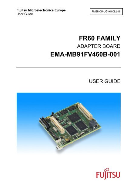
FR60 FAMILY EMA-MB91FV460B-001 - Fujitsu
FR60 FAMILY EMA-MB91FV460B-001 - Fujitsu
FR60 FAMILY EMA-MB91FV460B-001 - Fujitsu

You also want an ePaper? Increase the reach of your titles
YUMPU automatically turns print PDFs into web optimized ePapers that Google loves.
<strong>Fujitsu</strong> Microelectronics Europe<br />
User Guide<br />
FMEMCU-UG-910082-16<br />
<strong>FR60</strong> <strong>FAMILY</strong><br />
ADAPTER BOARD<br />
<strong>EMA</strong>-<strong>MB91FV460B</strong>-<strong>001</strong><br />
USER GUIDE
Revision History<br />
<strong>EMA</strong>-<strong>MB91FV460B</strong>-<strong>001</strong><br />
Revision History<br />
Date Issue<br />
2008-11-14 V1.0 AW<br />
First draft<br />
2009-01-14 V1.1 AW/CEy<br />
topICE settings added, defined “old”/”new” devices in Series Mode table,<br />
added information to APIX Interface chapter, corrected China RoHS, some<br />
minor improved descriptions<br />
2009-03-13 V1.2 CEy<br />
Restructured whole document, added new chapters (e.g. Quick Start<br />
Overview), improved existing chapters and figures (e.g. jumper overview)<br />
2009-04-07 V1.3 CEy<br />
Corrected memory map in chapter 5, changed wording of “old” and “new” in<br />
S100-2..4 description<br />
2009-04-14 V1.4 CEy<br />
Added description of Boot Flash programming via Softune Workbench<br />
(chapter 6.1.1), improved description of Main Flash programming<br />
2009-05-28 V1.5 CEy<br />
Updated disclaimer to new FME standard disclaimer, added troubleshooting<br />
chapter 8, corrected usable Emulation SRAM size<br />
2009-02-01 V1.6 CEy<br />
Added information about new FPGA revision with trace bugfix and the new<br />
feature of FPGA version output. Enhanced Troubleshooting chapter.<br />
Updated disclaimer, recycling and China RoHS information<br />
These were the latest revisions of related documents when this user guide revision had been<br />
released:<br />
Schematic: 1.4<br />
PCB: 1.3<br />
FPGA: 1.2<br />
This document contains 48 pages.<br />
UG-910082-16 - 2 - © <strong>Fujitsu</strong> Microelectronics Europe GmbH
Warranty and Disclaimer<br />
<strong>EMA</strong>-<strong>MB91FV460B</strong>-<strong>001</strong><br />
Warranty and Disclaimer<br />
The use of the deliverables (e.g. software, application examples, target boards, evaluation boards,<br />
starter kits, schematics, engineering samples of IC’s etc.) is subject to the conditions of <strong>Fujitsu</strong><br />
Microelectronics Europe GmbH (“FME”) as set out in (i) the terms of the License Agreement and/or<br />
the Sale and Purchase Agreement under which agreements the Product has been delivered, (ii) the<br />
technical descriptions and (iii) all accompanying written materials.<br />
Please note that the deliverables are intended for and must only be used for reference in an<br />
evaluation laboratory environment.<br />
The software deliverables are provided on an as-is basis without charge and are subject to<br />
alterations. It is the user’s obligation to fully test the software in its environment and to ensure proper<br />
functionality, qualification and compliance with component specifications.<br />
Regarding hardware deliverables, FME warrants that they will be free from defects in material and<br />
workmanship under use and service as specified in the accompanying written materials for a duration<br />
of 1 year from the date of receipt by the customer.<br />
Should a hardware deliverable turn out to be defect, FME’s entire liability and the customer’s<br />
exclusive remedy shall be, at FME´s sole discretion, either return of the purchase price and the<br />
license fee, or replacement of the hardware deliverable or parts thereof, if the deliverable is returned<br />
to FME in original packing and without further defects resulting from the customer’s use or the<br />
transport. However, this warranty is excluded if the defect has resulted from an accident not<br />
attributable to FME, or abuse or misapplication attributable to the customer or any other third party not<br />
relating to FME or to unauthorised decompiling and/or reverse engineering and/or disassembling.<br />
FME does not warrant that the deliverables do not infringe any third party intellectual property right<br />
(IPR). In the event that the deliverables infringe a third party IPR it is the sole responsibility of the<br />
customer to obtain necessary licenses to continue the usage of the deliverable.<br />
In the event the software deliverables include the use of open source components, the provisions of<br />
the governing open source license agreement shall apply with respect to such software deliverables.<br />
To the maximum extent permitted by applicable law FME disclaims all other warranties, whether<br />
express or implied, in particular, but not limited to, warranties of merchantability and fitness for a<br />
particular purpose for which the deliverables are not designated.<br />
To the maximum extent permitted by applicable law, FME’s liability is restricted to intention and gross<br />
negligence. FME is not liable for consequential damages.<br />
Should one of the above stipulations be or become invalid and/or unenforceable, the remaining<br />
stipulations shall stay in full effect.<br />
The contents of this document are subject to change without a prior notice, thus contact FME about<br />
the latest one.<br />
© <strong>Fujitsu</strong> Microelectronics Europe GmbH - 3 - UG-910082-16
Contents<br />
<strong>EMA</strong>-<strong>MB91FV460B</strong>-<strong>001</strong><br />
Contents<br />
REVISION HISTORY............................................................................................................ 2<br />
WARRANTY AND DISCLAIMER ......................................................................................... 3<br />
CONTENTS .......................................................................................................................... 4<br />
1 INTRODUCTION.............................................................................................................. 6<br />
1.1 Abstract................................................................................................................... 6<br />
1.2 General Description................................................................................................. 8<br />
1.3 Features.................................................................................................................. 9<br />
1.4 Important precautions and hints ............................................................................ 10<br />
1.5 System Overview .................................................................................................. 11<br />
2 INSTALLATION ............................................................................................................. 13<br />
2.1 Assembly............................................................................................................... 13<br />
2.2 Power on / off sequence........................................................................................ 14<br />
2.3 Disassembly instructions....................................................................................... 15<br />
3 QUICK START OVERVIEW........................................................................................... 17<br />
4 OPERATION.................................................................................................................. 18<br />
4.1 Jumpers, Connectors, Switches and LEDs Overview ............................................ 18<br />
4.1.1 Jumper Overview..................................................................................... 18<br />
4.1.2 Connector Overview ................................................................................ 18<br />
4.1.3 Switches Overview .................................................................................. 19<br />
4.1.4 LED Overview.......................................................................................... 19<br />
4.2 Location of Parts ................................................................................................... 20<br />
4.3 Detailed Jumper, Connectors, Switches and LED Description............................... 23<br />
4.3.1 Power supply on / off (SW 400 / J408)..................................................... 23<br />
4.3.2 Power supply jumper setting (J400)......................................................... 23<br />
4.3.3 Power supply fault LED (D400)................................................................ 23<br />
4.3.4 ADC reference voltage jumper setting (J401) .......................................... 24<br />
4.3.5 ADC supply jumper setting (J402) ........................................................... 24<br />
4.3.6 Crystal Select (J100) ............................................................................... 24<br />
4.3.7 FPGA mode control (S100-1)................................................................... 25<br />
4.3.8 FPGA mode [2..0] (S100-2..4) ................................................................. 25<br />
4.3.9 SER mode [2..0] (S100-2..4).................................................................... 26<br />
4.3.10 HWWDG_KILL (S100-8).......................................................................... 27<br />
4.3.11 FIX_EN# (S101-1) ................................................................................... 27<br />
UG-910082-16 - 4 - © <strong>Fujitsu</strong> Microelectronics Europe GmbH
<strong>EMA</strong>-<strong>MB91FV460B</strong>-<strong>001</strong><br />
Contents<br />
4.3.12 SRAM_SF# (S101-2)............................................................................... 27<br />
4.3.13 CSV_KILL (S101-3) ................................................................................. 27<br />
4.3.14 FSC_DISABLE (S101-4).......................................................................... 28<br />
4.3.15 EDSU_BREAK# (S101-5)........................................................................ 28<br />
4.3.16 FPGA control [0..2] (S101-6..8)................................................................ 28<br />
4.3.17 FPGA ready LED (D303) ......................................................................... 29<br />
4.3.18 Reset (INITx) LED (D302)........................................................................ 29<br />
4.3.19 LED D301................................................................................................ 29<br />
4.3.20 LED D300................................................................................................ 29<br />
4.3.21 APIX Interface (CON100) ........................................................................ 30<br />
4.3.22 Programming Adapter (J101, J102, CON101) ......................................... 31<br />
5 EXTERNAL EMULATION SRAM / INTERNAL FLASH MEMORY ................................ 33<br />
6 PROGRAMMING ........................................................................................................... 34<br />
6.1 Programming the BootFlash.................................................................................. 34<br />
6.1.1 Via Softune Workbench ........................................................................... 34<br />
6.1.2 Via FME FR Programmer ........................................................................ 35<br />
6.2 Programming the (main) Flash memory ................................................................ 37<br />
7 PRECAUTIONS WHEN USING SOCKET ADAPTER BOARDS ................................... 38<br />
7.1 Using <strong>EMA</strong>-MB91F460x-xxxMxx ........................................................................... 38<br />
7.2 Common precautions for NLS and LS boards ....................................................... 38<br />
7.3 Using <strong>EMA</strong>-MB91F46xx-NLS-xxxMxx ................................................................... 39<br />
7.4 Using <strong>EMA</strong>-MB91F46xx-LS-xxxMxx...................................................................... 40<br />
8 TROUBLESHOOTING ................................................................................................... 41<br />
9 MECHANICAL DIMENSIONS........................................................................................ 42<br />
10 PCB HISTORY............................................................................................................... 43<br />
10.1 <strong>EMA</strong>-<strong>MB91FV460B</strong>-<strong>001</strong> PCB Rev. 1.3.................................................................. 43<br />
11 FPGA HISTORY ............................................................................................................ 44<br />
11.1 <strong>EMA</strong>-<strong>MB91FV460B</strong>-<strong>001</strong> FPGA Rev. 1.0 ............................................................... 44<br />
11.2 <strong>EMA</strong>-<strong>MB91FV460B</strong>-<strong>001</strong> FPGA Rev. 1.1 ............................................................... 44<br />
11.3 <strong>EMA</strong>-<strong>MB91FV460B</strong>-<strong>001</strong> FPGA Rev. 1.2 ............................................................... 44<br />
12 INFORMATION IN THE WWW....................................................................................... 46<br />
13 CHINA-ROHS REGULATION ........................................................................................ 47<br />
14 RECYCLING .................................................................................................................. 48<br />
© <strong>Fujitsu</strong> Microelectronics Europe GmbH - 5 - UG-910082-16
1 Introduction<br />
1.1 Abstract<br />
<strong>EMA</strong>-<strong>MB91FV460B</strong>-<strong>001</strong><br />
Chapter 1 Introduction<br />
The <strong>EMA</strong>-<strong>MB91FV460B</strong>-<strong>001</strong> is an adapter board for the <strong>Fujitsu</strong> MB91460 Series<br />
microcontroller.<br />
The board can be equipped with different socket adapter boards to replace different<br />
MB91460 family based microcontrollers. The board allows the designer immediately to start<br />
with the software development before the appropriate silicon samples are available.<br />
This board must only be used for test applications<br />
in an evaluation laboratory environment.<br />
Before using the <strong>EMA</strong>-<strong>MB91FV460B</strong>-<strong>001</strong> adapter board, make sure that the following<br />
packed components have been delivered:<br />
o 1 pcs. <strong>EMA</strong>-<strong>MB91FV460B</strong>-<strong>001</strong> board (1)<br />
o 1 pcs. Programming adapter (2) + 2 x screws<br />
o 1 pcs. AC adapter 5V / > 1500mA (3)<br />
o 1 pcs. Adapter cable for MB2198-10 in-circuit emulator (4)<br />
o 1 pcs. User Guide<br />
o 1 pcs. Micros DVD<br />
o 1 pcs. <strong>EMA</strong> Disassembly Kit, consisting of<br />
1 x Screwdriver Torx TX8 (A)<br />
1 x Spanner M5 (B)<br />
5 x Screws DIN 7985 A2 M2,5X30 TX8, 1 spare (C)<br />
5 x Bolts M2,5 X 8, 1 spare (D)<br />
5 x Sockets, 1 spare (E)<br />
UG-910082-16 - 6 - © <strong>Fujitsu</strong> Microelectronics Europe GmbH
1<br />
3<br />
C D<br />
E<br />
Figure 1-1: System components overview<br />
3<br />
<strong>EMA</strong>-<strong>MB91FV460B</strong>-<strong>001</strong><br />
Chapter 1 Introduction<br />
3<br />
4<br />
© <strong>Fujitsu</strong> Microelectronics Europe GmbH - 7 - UG-910082-16<br />
A<br />
B<br />
2<br />
3
1.2 General Description<br />
<strong>EMA</strong>-<strong>MB91FV460B</strong>-<strong>001</strong><br />
Chapter 1 Introduction<br />
The <strong>EMA</strong>-<strong>MB91FV460B</strong>-<strong>001</strong> in combination with a socket adapter board replaces a<br />
MB91460 family based microcontroller. An Emulation SRAM (512k x 64 Bit) is connected to<br />
the F-Bus memory resources.<br />
Figure 1-2: <strong>EMA</strong>-<strong>MB91FV460B</strong>-<strong>001</strong> overview<br />
The board is supplied with a 4MHz crystal as the main oscillation clock. Using the internal<br />
PLL of the MCU, internal clock rates up to 100MHz (see datasheet) can be achieved.<br />
Alternatively a crystal on the target board can be connected to the <strong>MB91FV460B</strong> oscillator<br />
(J100).<br />
Additionally a 32kHz crystal is mounted for use as a sub clock.<br />
A programming adapter can be connected to the <strong>EMA</strong>-<strong>MB91FV460B</strong>-<strong>001</strong> board.<br />
The operating mode of the microcontroller (MD0, MD1, MD2) and the reset signal (INITX)<br />
can be controlled by the target board or by the <strong>EMA</strong>-<strong>MB91FV460B</strong>-<strong>001</strong> board.<br />
UG-910082-16 - 8 - © <strong>Fujitsu</strong> Microelectronics Europe GmbH
1.3 Features<br />
<strong>EMA</strong>-<strong>MB91FV460B</strong>-<strong>001</strong><br />
Chapter 1 Introduction<br />
The following points describe some of the features of the <strong>EMA</strong>-<strong>MB91FV460B</strong>-<strong>001</strong> with<br />
evaluation chip <strong>MB91FV460B</strong>. Especially the differences to the old <strong>EMA</strong>-MB91V460A-<br />
002B/-80/-003 with evaluation chip MB91V460A are pointed out.<br />
The <strong>MB91FV460B</strong> has 2112 kB of internal Flash memory. Furthermore, there are<br />
4 MB SRAM mounted on <strong>EMA</strong>-<strong>MB91FV460B</strong>-<strong>001</strong> for use as external emulation<br />
memory (only 2112KB usable). The user can switch between Flash memory and<br />
Emulation SRAM. The sectors can be configured via register ROMS to match the<br />
size and location of the MB91460 Series MCU for which the user is developing.<br />
The <strong>MB91FV460B</strong> now has split power domains VDD5 and VDD35 that can be<br />
independently set to 5 V or 3.3 V on <strong>EMA</strong>-<strong>MB91FV460B</strong>-<strong>001</strong>. This means that socket<br />
adapter boards with level-shifters are not longer required!<br />
<strong>MB91FV460B</strong> supports a maximum core frequency of 100 MHz<br />
<strong>MB91FV460B</strong> is equipped with 16 KB BootFlash memory. This BootFlash memory<br />
allows the user to program the BootROM code that is used by the MB91460 Series<br />
MCU for which the user is developing. To change the BootROM code in the<br />
BootFlash memory a special procedure must be executed that is described in<br />
chapter 6.1<br />
<strong>MB91FV460B</strong> covers the whole functionality of at least all currently (January 2009)<br />
available MB91460 Series MCU, including e.g. APIX, FlexRay and MediaLB.<br />
Therefore, extensions boards such as <strong>EMA</strong>-MB91V460A-100 (FlexRay) and <strong>EMA</strong>-<br />
MB91V460A-300 (APIX) are not longer required.<br />
There are several MB91460 Series MCU with a special port multiplexing functionality<br />
(e.g. MB91460P) or a non-standard port layout (e.g. MB91460Q). All these modes<br />
are now supported by <strong>MB91FV460B</strong> and can be set with switches on <strong>EMA</strong>-<br />
<strong>MB91FV460B</strong>-<strong>001</strong>.<br />
<strong>EMA</strong>-<strong>MB91FV460B</strong>-<strong>001</strong> combines the trace features of the former <strong>EMA</strong>-<br />
MB91V460A-002B/-80 and <strong>EMA</strong>-MB91V460A-003. This means there is an on-board<br />
trace memory for 64 k frames. Alternatively you can connect the SuperTraceProbe<br />
from GreenHills Software Inc. to gather trace data.<br />
© <strong>Fujitsu</strong> Microelectronics Europe GmbH - 9 - UG-910082-16
1.4 Important precautions and hints<br />
<strong>EMA</strong>-<strong>MB91FV460B</strong>-<strong>001</strong><br />
Chapter 1 Introduction<br />
Please check the following points before using <strong>EMA</strong>-<strong>MB91FV460B</strong>-<strong>001</strong>:<br />
Follow the instructions in chapter 2.1/ 2.3 when mounting/dismounting the <strong>EMA</strong>-<br />
<strong>MB91FV460B</strong>-<strong>001</strong> to/from socket adapter boards.<br />
Only use the delivered power supply unit! <strong>EMA</strong>-<strong>MB91FV460B</strong>-<strong>001</strong> is directly<br />
supplied with 5V from the external power supply unit. When using other power<br />
supply units with different output voltages, a red warning LED will light. Protective<br />
measures are implemented on <strong>EMA</strong>-<strong>MB91FV460B</strong>-<strong>001</strong> to prevent damage in such<br />
cases.<br />
Remove or attach the cable between <strong>EMA</strong>-<strong>MB91FV460B</strong>-<strong>001</strong> and DSU MB2198-<br />
10 only when power of both systems is off.<br />
Check the jumper settings for VDD5 and VDD35 and compare them with the target<br />
board settings before switching power on. You can probably use the settings in the<br />
Quick Start Overview (chapter 3) as a basic configuration.<br />
Follow the power off/on sequence described in chapter 2.2<br />
When using socket adapter boards, especially those of (old) type <strong>EMA</strong>-MB91F46x-<br />
NLS-xxxMxx or <strong>EMA</strong>-MB91F46x-LS-xxxMxx, please refer to chapter 7 for a<br />
description of the necessary settings<br />
When using <strong>EMA</strong>-<strong>MB91FV460B</strong>-<strong>001</strong> in stand-alone operation (without socket<br />
adapters and target board connected refer to the Quick Start Overview (chapter 3)<br />
for the necessary settings<br />
UG-910082-16 - 10 - © <strong>Fujitsu</strong> Microelectronics Europe GmbH
1.5 System Overview<br />
Figure 1-3: System overview<br />
<strong>EMA</strong>-<strong>MB91FV460B</strong>-<strong>001</strong><br />
Chapter 1 Introduction<br />
The <strong>EMA</strong>-<strong>MB91FV460B</strong>-<strong>001</strong> can be used in combination with the following emulation<br />
devices:<br />
<strong>Fujitsu</strong> MB2198 emulator system (MB2198-01 with MB2198-10)<br />
GHS Super Trace Probe emulator (also a <strong>Fujitsu</strong> MB2198 emulator system is<br />
required)<br />
Accemic topICE emulator<br />
Figure 1-4: Configuration 1: <strong>EMA</strong>-<strong>MB91FV460B</strong>-<strong>001</strong> and <strong>Fujitsu</strong> MB2198 in-circuit-emulator<br />
system<br />
© <strong>Fujitsu</strong> Microelectronics Europe GmbH - 11 - UG-910082-16
<strong>EMA</strong>-<strong>MB91FV460B</strong>-<strong>001</strong><br />
Chapter 1 Introduction<br />
Figure 1-5: Configuration 2: <strong>EMA</strong>-<strong>MB91FV460B</strong>-<strong>001</strong> and GHS Super Trace Probe / <strong>Fujitsu</strong><br />
MB2198 in-circuit-emulator system<br />
Figure 1-6: Configuration 3: <strong>EMA</strong>-<strong>MB91FV460B</strong>-<strong>001</strong> and Accemic topICE in-circuit-emulator<br />
system<br />
UG-910082-16 - 12 - © <strong>Fujitsu</strong> Microelectronics Europe GmbH
2 Installation<br />
2.1 Assembly<br />
<strong>EMA</strong>-<strong>MB91FV460B</strong>-<strong>001</strong><br />
Chapter 2 Installation<br />
Remove carefully the <strong>EMA</strong>-<strong>MB91FV460B</strong>-<strong>001</strong> board from the shipping carton and check if<br />
there are any damages.<br />
Install the socket adapter board, as described in the specific socket adapter board manual.<br />
Please check very carefully the exact adjustment.<br />
Switch off the power supply of the target board, the <strong>EMA</strong>-<strong>MB91FV460B</strong>-<strong>001</strong> and other<br />
connected devices.<br />
Optionally, fix the <strong>EMA</strong>-<strong>MB91FV460B</strong>-<strong>001</strong> adapter board by using M2.5 screws and M2.5<br />
fibre washers.<br />
Screw<br />
M2.5 x 12<br />
(optional)<br />
Washer<br />
M2.5 (Fiber)<br />
(optional)<br />
120,8 mm<br />
Target board<br />
Figure 2-1: <strong>EMA</strong>-<strong>MB91FV460B</strong>-<strong>001</strong> system installation<br />
DSU4 SSRAM, Emulation RAM<br />
<strong>MB91FV460B</strong><br />
Connector for extension board<br />
<strong>EMA</strong>-<strong>MB91FV460B</strong>-<strong>001</strong><br />
Connector <strong>EMA</strong>-<strong>MB91FV460B</strong>-<strong>001</strong><br />
to socket adapter board<br />
Socket adapter board<br />
© <strong>Fujitsu</strong> Microelectronics Europe GmbH - 13 - UG-910082-16
2.2 Power on / off sequence<br />
<strong>EMA</strong>-<strong>MB91FV460B</strong>-<strong>001</strong><br />
Chapter 2 Installation<br />
After power-on of the <strong>EMA</strong>-<strong>MB91FV460B</strong>-<strong>001</strong> board, the blue power-on LED (D303) should<br />
be on. If the LED is off, turn off the power supply and check the default jumper and switch<br />
settings.<br />
If the red over-voltage / over-current warning LED (D400) is on or blinking, either the input<br />
voltage is higher than 5.25V or the current consumption is too high.<br />
Please remove or attach the cable between <strong>EMA</strong>-<strong>MB91FV460B</strong>-<strong>001</strong> and<br />
MB2198-10 only when power of both systems is off.<br />
<strong>EMA</strong>-<strong>MB91FV460B</strong>-<strong>001</strong> / MB2198-01 power on sequence<br />
1. Turn MB2198-01 power on.<br />
2. Turn <strong>EMA</strong>-<strong>MB91FV460B</strong>-<strong>001</strong> power on.<br />
3. Turn target board power on (if connected)<br />
<strong>EMA</strong>-<strong>MB91FV460B</strong>-<strong>001</strong> / MB2198-01 power off sequence<br />
1. Turn target board power off (if connected).<br />
2. Turn <strong>EMA</strong>-<strong>MB91FV460B</strong>-<strong>001</strong> power off.<br />
3. Turn MB2198 power off<br />
UG-910082-16 - 14 - © <strong>Fujitsu</strong> Microelectronics Europe GmbH
2.3 Disassembly instructions<br />
<strong>EMA</strong>-<strong>MB91FV460B</strong>-<strong>001</strong><br />
Chapter 2 Installation<br />
Because the connectors can be damaged by awkwardly disassembling, it is strongly<br />
recommended to use the enclosed disassembly components and strictly follow the described<br />
disassembly instructions.<br />
E<br />
Strictly follow the described disassembly instructions.<br />
Otherwise, the board connectors may be damaged.<br />
E<br />
E<br />
I.) Put sockets in holes of <strong>EMA</strong> socket<br />
adapter board. (only 3 visible in picture)<br />
III.) After you have executed steps II and III<br />
four times. The situation should be similar<br />
to the one in the picture above<br />
II.) Lay a bolt on top of one socket. Turn a<br />
screw with one hand and hold the bolt with<br />
the other hand. Turn so far that the bolt<br />
touches the upper <strong>EMA</strong> board.<br />
IV.) Hold the bolts with the spanner (or your<br />
fingers if possible) and ...<br />
© <strong>Fujitsu</strong> Microelectronics Europe GmbH - 15 - UG-910082-16
V.) ...turn the screws clockwise in small<br />
steps in the following sequence: 1-2-3-4-1-<br />
2-3-4-1-... and so on until you can easily<br />
dismount the upper <strong>EMA</strong> board<br />
Caution:<br />
Lift the sides equally! Avoid canting!<br />
Table 2-1: Disassembly process<br />
<strong>EMA</strong>-<strong>MB91FV460B</strong>-<strong>001</strong><br />
Chapter 2 Installation<br />
VI.) Finished!<br />
UG-910082-16 - 16 - © <strong>Fujitsu</strong> Microelectronics Europe GmbH
3 Quick Start Overview<br />
<strong>EMA</strong>-<strong>MB91FV460B</strong>-<strong>001</strong><br />
Chapter 3 Quick Start Overview<br />
The following overview table contains settings that will most likely allow you to use<br />
<strong>EMA</strong>-<strong>MB91FV460B</strong>-<strong>001</strong> without having to read the whole User Guide in detail. The settings<br />
apply to the most common use cases. For the location and numbering of the jumpers and<br />
switches see chapter 4.2<br />
Item Ref. 1<br />
S100-1<br />
FPGA_MD_CTRL<br />
S100-[2:4]<br />
FPGA_MD_[2:0]<br />
S100-[5:7]<br />
SER_MD_[2:0]<br />
S100-8<br />
HWWDG_KILL<br />
S101-1<br />
FIX_EN#<br />
S101-2<br />
SRAM_SF#<br />
S101-3<br />
CSV_KILL<br />
S101-4<br />
FSC_DISABLE<br />
S101-5<br />
EDSU_BREAK#<br />
S101-[6:8]<br />
FPGA_CTRL[0:2]<br />
J400-2,4,6<br />
VDD5<br />
J400-1,3,5<br />
VDD35<br />
J401-1,3,5<br />
AVRH0<br />
J401-2,4,6<br />
AVRH1<br />
J402-1,3,5<br />
AVCC0<br />
J402-2,4,6<br />
AVCC1<br />
J100-1,3,5 / 2,4,6<br />
X0 / X1<br />
J101-1,2,3,4,5<br />
SIN select<br />
J102-1,2,3,4,5<br />
SOT select<br />
Standalone<br />
4.3.7 ON<br />
<strong>EMA</strong>-MB91F460x-<br />
2, 3<br />
xxxMxx<br />
Operation Modes<br />
<strong>EMA</strong>-MB91F46xx-<br />
2, 3<br />
NLS-xxxMxx<br />
OFF<br />
(Mode pins MD[2:0] taken from target board)<br />
4.3.8 OFF, OFF, OFF don’t care<br />
4.3.9 Series Mode: Dependent on the device to be emulated<br />
4.3.10 ON 4<br />
4.3.11 ON<br />
4.3.12,<br />
5, 6.2<br />
<strong>EMA</strong>-MB91F46xx-<br />
2, 3<br />
LS-xxxMxx<br />
© <strong>Fujitsu</strong> Microelectronics Europe GmbH - 17 - UG-910082-16<br />
OFF<br />
4.3.13 ON<br />
4.3.14 OFF<br />
4.3.15 OFF<br />
4.3.16 OFF, OFF, OFF<br />
4.3.2,<br />
7<br />
4.3.2,<br />
7<br />
4.3.4,<br />
7<br />
4.3.4,<br />
7<br />
4.3.5,<br />
7<br />
4.3.5,<br />
7<br />
4.3.6<br />
4.3.22<br />
4.3.22<br />
don’t care Match target board VDD5 setting!<br />
don’t care Match target board VDD35 setting! Match VDD5 setting!<br />
Close 3,5<br />
(AVRH0 = VDD5)<br />
Match AVRH0 setting (see above)!<br />
Close 3,5<br />
(AVCC0 = VDD5)<br />
Match AVCC0 setting (see above)!<br />
Close 1,3<br />
(AVRH0 = AVRH(0) target board)<br />
Close 4,6<br />
(AVRH1 = VDD5)<br />
Close 1,3<br />
(AVCC0 = AVCC(0) target board)<br />
Close 3,5 and 4,6<br />
(on-board 4MHz crystal)<br />
Close 4,6<br />
(AVCC1 = VDD5)<br />
Close 1,2 and 4,5<br />
(no SIN signal is routed to programming connector)<br />
Close 1,2 and 4,5<br />
(no SOT signal is routed to programming connector)<br />
1 For more information refer to the listed chapters<br />
2 It is assumed that also a target board is connected<br />
3 Please refer to chapter 7 for further advices when using socket adapter boards<br />
4 OFF for <strong>EMA</strong>-<strong>MB91FV460B</strong>-<strong>001</strong> prototypes with <strong>MB91FV460B</strong>1 with HW Watchdog Bug when not using workarounds
4 Operation<br />
<strong>EMA</strong>-<strong>MB91FV460B</strong>-<strong>001</strong><br />
Chapter 4 Operation<br />
4.1 Jumpers, Connectors, Switches and LEDs Overview<br />
This chapter describes all jumpers, connectors and switches that can be modified or<br />
accessed on the <strong>EMA</strong>-<strong>MB91FV460B</strong>-<strong>001</strong> adapter board.<br />
4.1.1 Jumper Overview<br />
Jumper Description / Function Type Default<br />
J100 Crystal select Jumper 3x2 pol 3-5, 4-6<br />
J101 Programming Connector SIN Jumper 5 pol 1-2, 4-5<br />
J102 Programming Connector SOT Jumper 5 pol 1-2, 4-5<br />
J400 VDD35 / VDD5 Jumper 3x2 pol 3-5, 2-4<br />
J401 AVRH 0/1 Jumper 3x2 pol 1-3, 2-4<br />
J402 AVCC 0/1 Jumper 3x2 pol 1-3, 2-4<br />
J300 Additional INITx input (not assembled) Jumper 2 pol ---<br />
J408<br />
Additional Power ON/OFF input<br />
(not assembled)<br />
Jumper 2 pol ---<br />
J606 5V supply for Accemic topICE Jumper 3 pol open<br />
4.1.2 Connector Overview<br />
Connector Description / Function Type Default<br />
CON100 APIX interface<br />
CON101 Flash programming interface<br />
CON102 MB2198 interface<br />
CON300 FPGA programming cable<br />
CON301 GHS STP connector<br />
CON400 5V power supply<br />
Molex<br />
540300471<br />
Molex<br />
530470510<br />
Molex<br />
903259020<br />
Molex<br />
903259010<br />
Mictor<br />
2-767004-2<br />
Switchcraft<br />
RAPC 722<br />
APIX cable<br />
Programming cable<br />
MB2198-10 cable<br />
Altera USB Blaster<br />
(via adapter cable)<br />
GHS STP cable<br />
Power supply 5V<br />
UG-910082-16 - 18 - © <strong>Fujitsu</strong> Microelectronics Europe GmbH
4.1.3 Switches Overview<br />
<strong>EMA</strong>-<strong>MB91FV460B</strong>-<strong>001</strong><br />
Chapter 4 Operation<br />
Switch Signal Description / Function Default<br />
S100-1 FPGA_MD_CTRL MD[2..0] control source OFF<br />
S100-2 FPGA_MD_2 MD[2..0] control<br />
OFF<br />
S100-3 FPGA_MD_1 (S100-1 must be ON for getting OFF<br />
S100-4 FPGA_MD_0<br />
FPGA_MD_[2:0] effective) OFF<br />
S100-5 SER_MD_2 OFF<br />
S100-6 SER _MD_1 SER_MD_[2..0] control<br />
OFF<br />
S100-7 SER _MD_0<br />
OFF<br />
S100-8 HWWDG_KILL Hardware Watchdog ON<br />
S101-1 FIX_EN# Fixed Mode / Reset Vector ON<br />
S101-2 SRAM_SF# Emulation SRAM / Internal Flash OFF<br />
S101-3 CSV_KILL Clock Supervisor ON<br />
S101-4 FSC_DISABLE Flash Security OFF<br />
S101-5 EDSU_BREAK# Embedded Debug Support Unit Break OFF<br />
S101-6 FPGA_CTRL0 Reserved for future use<br />
OFF<br />
S101-7 FPGA_CTRL1 OFF<br />
S101-8 FPGA_CTRL2<br />
OFF<br />
SW 400 Power on / off ON<br />
Note: “ON”/”OFF” does not necessarily indicate the logic level of the related signal. Please<br />
refer to the detailed description of each switch.<br />
4.1.4 LED Overview<br />
LED Colour Signal Description / Function Default<br />
D400 Red U402_FAULT Overvoltage / overcurrent warning OFF<br />
D303 Blue LED0 Operation ok ON<br />
D302 Yellow LED1 Reset active OFF<br />
D301 Yellow LED2 Reserved OFF<br />
D300 Red LED3 Reserved OFF<br />
Do not stare into LEDs or view directly with optical instruments.<br />
© <strong>Fujitsu</strong> Microelectronics Europe GmbH - 19 - UG-910082-16
4.2 Location of Parts<br />
5<br />
4<br />
3<br />
2<br />
1<br />
+5V, 1500 mA<br />
--(O-- +<br />
J101<br />
2<br />
4<br />
6<br />
5<br />
4<br />
3<br />
2<br />
1<br />
J804<br />
1<br />
3<br />
5<br />
2<br />
4<br />
6<br />
J102<br />
1<br />
3<br />
5<br />
J402 J401<br />
2.1<br />
mm<br />
5.5<br />
mm<br />
SW400<br />
<strong>EMA</strong>-<strong>MB91FV460B</strong>-<strong>001</strong><br />
Chapter 4 Operation<br />
J606<br />
1 8<br />
S101<br />
1 8<br />
S100<br />
6 4 2<br />
5 3 1<br />
UG-910082-16 - 20 - © <strong>Fujitsu</strong> Microelectronics Europe GmbH<br />
ON<br />
ON<br />
CON300<br />
Figure 4-1: Location of parts and default settings (top layer)<br />
J805<br />
J300<br />
J400<br />
5<br />
3<br />
1<br />
J408<br />
6<br />
4<br />
2<br />
J100<br />
D400<br />
5 4 3 2 1<br />
J804, J805 are connectors for extension boards on the top (e.g. Accemic topICE)<br />
D300<br />
D301<br />
D302<br />
D303<br />
CON101<br />
CON102<br />
CON301
R112<br />
R102<br />
R103<br />
R101<br />
R104<br />
CON100<br />
<strong>EMA</strong>-<strong>MB91FV460B</strong>-<strong>001</strong><br />
Chapter 4 Operation<br />
R105 R106<br />
© <strong>Fujitsu</strong> Microelectronics Europe GmbH - 21 - UG-910082-16<br />
J800<br />
J810 J803<br />
J802<br />
Figure 4-2: Location of parts (bottom layer)<br />
R109<br />
R108<br />
J801<br />
R107<br />
J800, J801, J802, J803, J810 are connectors for socket adapter boards or special extension<br />
boards
SIN<br />
SOT<br />
AVCC1<br />
AVCC0<br />
AVRH1<br />
AVRH0<br />
<strong>EMA</strong>-<strong>MB91FV460B</strong>-<strong>001</strong><br />
Chapter 4 Operation<br />
Power OFF<br />
Power ON<br />
Figure 4-3: Jumpers, switches and LEDs overview<br />
S101<br />
1 FIX_EN#<br />
2 SRAM_SF#<br />
3 CSV_KILL<br />
4 FSC_DISABLE<br />
5 EDSU_BREAK#<br />
6 FPGA_CTRL0<br />
7 FPGA_CTRL1<br />
8 FPGA_CTRL2<br />
S100<br />
1 FPGA_MD_CTRL<br />
2 FPGA_MD_2<br />
3 FPGA_MD_1<br />
4 FPGA_MD_0<br />
5 SER_MD_2<br />
6 SER_MD_1<br />
7 SER_MD_0<br />
8 HWWDG_KILL<br />
UG-910082-16 - 22 - © <strong>Fujitsu</strong> Microelectronics Europe GmbH<br />
3.3V<br />
5V<br />
X1<br />
X0
<strong>EMA</strong>-<strong>MB91FV460B</strong>-<strong>001</strong><br />
Chapter 4 Operation<br />
4.3 Detailed Jumper, Connectors, Switches and LED Description<br />
The default setting is shown with a grey shaded area.<br />
4.3.1 Power supply on / off (SW 400 / J408)<br />
SW400: power supply on<br />
J408 (not assembled) is a bypass for SW400.<br />
Switch State Description<br />
SW400<br />
ON<br />
OFF<br />
Power supply on<br />
Power supply off<br />
Default: SW400: ON, J408: open (not assembled)<br />
4.3.2 Power supply jumper setting (J400)<br />
J400: defines the voltage of VDD5 and VDD35<br />
Jumper Setting Description<br />
1-3 VDD35 is connected to 5V.<br />
Be sure that the target board accepts 5V signals<br />
J400 1,3,5<br />
(VDD35) 3-5<br />
on the pins of the VDD35 domain!<br />
VDD35 is connected to 3.3V<br />
With this setting the target board is not allowed to<br />
supply 5V level signals to the <strong>EMA</strong>-<strong>MB91FV460B</strong>-<br />
<strong>001</strong> board on the pins of the VDD35 domain!<br />
2-4 VDD5 is connected to 5V<br />
J400 2,4,6<br />
(VDD5)<br />
Default: J400 3-5, 2-4<br />
4-6<br />
Be sure that the target board accepts 5V signals<br />
on the pins of the VDD5 domain!<br />
VDD5 is connected to 3.3V<br />
With this setting the target board is not allowed to<br />
supply 5V level signals to the <strong>EMA</strong>-<strong>MB91FV460B</strong>-<br />
<strong>001</strong> board on the pins of the VDD5 domain!<br />
4.3.3 Power supply fault LED (D400)<br />
D400: U402_FAULT output<br />
LED State Description<br />
D400<br />
Default: D400: OFF<br />
ON (red)<br />
Input voltage > 5.25V or current consumption too<br />
high<br />
OFF Supply voltage ok<br />
© <strong>Fujitsu</strong> Microelectronics Europe GmbH - 23 - UG-910082-16
<strong>EMA</strong>-<strong>MB91FV460B</strong>-<strong>001</strong><br />
Chapter 4 Operation<br />
4.3.4 ADC reference voltage jumper setting (J401)<br />
J401: defines the AVRH0 / AVRH1 source<br />
Jumper Setting Description<br />
J401 1,3,5 1-3 AVRH0 is connected to AVRH0_T (target board).<br />
(AVRH 0) 3-5 AVRH0 is connected to VDD5<br />
J401 2,4,6 2-4 AVRH1 is connected to AVRH1_T (target board)<br />
(AVRH 1) 4-6 AVRH1 is connected to VDD5<br />
Default: J401 1-3, 2-4<br />
<strong>MB91FV460B</strong> includes 2 ADC with separate analogue high reference inputs.<br />
4.3.5 ADC supply jumper setting (J402)<br />
J402: defines the AVCC0 / AVCC1 source<br />
Jumper Setting Description<br />
J402 1,3,5 1-3 AVCC0 is connected to AVCC0_T (target board)<br />
(AVCC 0) 3-5 AVCC0 is connected to VDD5<br />
J402 2,4,6 2-4 AVCC1 is connected to AVCC1_T (target board)<br />
(AVCC 1)<br />
Default: J402 1-3, 2-4<br />
4-6 AVCC1 is connected to VDD5<br />
<strong>MB91FV460B</strong> includes 2 ADC with separate analogue supply inputs.<br />
4.3.6 Crystal Select (J100)<br />
J100: defines the X0 / X1 source<br />
Jumper Setting Description<br />
J100 2,4,6<br />
(X0)<br />
2-4<br />
4-6<br />
X0 of <strong>MB91FV460B</strong> is connected to the socket<br />
adapter board (J801-55)<br />
X0 of <strong>MB91FV460B</strong> is connected to the onboard<br />
4MHz crystal (Y101)<br />
1-3 X1 of <strong>MB91FV460B</strong> is connected to the socket<br />
J100 1,3,5<br />
adapter board (J801-54)<br />
(X1)<br />
Default: J100 3-5, 4-6<br />
3-5 X1 of <strong>MB91FV460B</strong> is connected to the onboard<br />
4MHz crystal (Y101)<br />
UG-910082-16 - 24 - © <strong>Fujitsu</strong> Microelectronics Europe GmbH
4.3.7 FPGA mode control (S100-1)<br />
<strong>EMA</strong>-<strong>MB91FV460B</strong>-<strong>001</strong><br />
Chapter 4 Operation<br />
Switch Setting Description<br />
S100-1<br />
(FPGA_MD<br />
_CTRL) ON (GND)<br />
OFF (VDD5) MD[2:0] pins are controlled by the target board.<br />
MD[2:0] pins are controlled by the FPGA according<br />
to the S100-2..4 (FPGA_MD_[2:0]) setting.<br />
Default: S100-1: OFF<br />
You can either configure the MD[2:0] pins of <strong>MB91FV460B</strong> by on-board DIP switches S100-<br />
2..4 (necessary for stand-alone operation) or you can derive them from a connected target<br />
board.<br />
4.3.8 FPGA mode [2..0] (S100-2..4)<br />
The MD[2:0] pins are controlled by the FPGA when S100-1 is ON.<br />
Switch<br />
S100-2..4<br />
(FPGA_MD_[2:0])<br />
Setting<br />
MD Description<br />
S100-2 S100-3 S100-4 [2:0]<br />
OFF OFF OFF 0 0 0 Internal ROM mode<br />
OFF OFF ON 0 0 1 External ROM mode<br />
OFF ON OFF 0 1 0 Reserved<br />
OFF ON ON 0 1 1 Reserved<br />
ON OFF OFF 1 0 0 Fallback BootROM<br />
ON OFF ON 1 0 1 Reserved<br />
ON ON OFF 1 1 0 Reserved<br />
ON<br />
Default: S100-2..4: OFF OFF OFF<br />
ON ON 1 1 1 Reserved<br />
(Note, the level of FPGA_MD_[2:0] will be inverted by the FPGA, so that “OFF” equals “0”.)<br />
© <strong>Fujitsu</strong> Microelectronics Europe GmbH - 25 - UG-910082-16
4.3.9 SER mode [2..0] (S100-2..4)<br />
Switch<br />
S100-5..7<br />
(SER_MD_[2:0])<br />
<strong>EMA</strong>-<strong>MB91FV460B</strong>-<strong>001</strong><br />
Chapter 4 Operation<br />
S100-5<br />
Setting<br />
S100-6 S100-7<br />
Default: S100-5..7: OFF OFF OFF<br />
SER_MD<br />
[2:0]<br />
OFF OFF OFF 0 0 0<br />
OFF OFF ON 0 0 1<br />
OFF ON OFF 0 1 0<br />
OFF ON ON 0 1 1<br />
ON OFF OFF 1 0 0<br />
ON OFF ON 1 0 1<br />
Description<br />
ON ON OFF 1 1 0 Reserved<br />
ON ON ON 1 1 1<br />
External bus is enabled after<br />
INIT (PFR,EPFR=1).<br />
Default mode for emulation of<br />
the following MCUs:<br />
MB91F464A, MB91F465K,<br />
MB91F465C/467C,<br />
MB91F465D/467D,<br />
MB91F469G<br />
Enable pin multiplexing for<br />
MB91460P and T series,<br />
external bus is disabled after<br />
INIT in internal vector fetch<br />
mode (MD=000)<br />
MB91461 mode, supports<br />
special clock features of<br />
MB91461, but does not<br />
support the separated power<br />
domains of MB91461 IO ring<br />
Enable pin multiplexing for<br />
MB91460B series, emulates<br />
the "no external bus" mode<br />
(MD3=0), for "external bus<br />
mode" (MD3=1) use<br />
SER_MD=000<br />
Interrupt relocation for<br />
MB91460M series<br />
Interrupt relocation for<br />
MB91460Q series, external<br />
bus is disabled after INIT in<br />
internal vector fetch mode<br />
(MD=000)<br />
External bus is disabled after<br />
INIT (PFR,EPFR=0) in<br />
internal vector fetch mode<br />
(MD=000).<br />
Default mode for emulation of<br />
all other MCUs not<br />
mentioned elsewhere in this<br />
table.<br />
UG-910082-16 - 26 - © <strong>Fujitsu</strong> Microelectronics Europe GmbH
4.3.10 HWWDG_KILL (S100-8)<br />
<strong>EMA</strong>-<strong>MB91FV460B</strong>-<strong>001</strong><br />
Chapter 4 Operation<br />
Switch Setting Description<br />
S100-8 ON (GND) Hardware-Watchdog is enabled<br />
(HWWDG_KILL)<br />
OFF (VDD5) Hardware-Watchdog is disabled<br />
Default: S100-8: ON<br />
The Hardware-Watchdog of <strong>MB91FV460B</strong> can be permanently disabled when setting this<br />
switch to OFF<br />
4.3.11 FIX_EN# (S101-1)<br />
Switch Setting Description<br />
S101-1 ON (GND) Fixed Mode / Reset Vector is enabled<br />
(FIX_EN# )<br />
Default: ON<br />
OFF (VDD5) Fixed Mode / Reset Vector is disabled<br />
When Fixed Mode / Reset Vector is enabled, the mode vector at address 0x000f:fff8 and the<br />
reset vector at address 0x000f:fffc cannot be changed and always return fixed values.<br />
4.3.12 SRAM_SF# (S101-2)<br />
Switch Setting Description<br />
S101-2 ON (GND) Internal Flash Mode<br />
(SRAM_SF# )<br />
Default: OFF<br />
OFF (VDD5) External Emulation SRAM Mode<br />
With this switch you can define whether the internal Flash memory or the external Emulation<br />
SRAM is connected to the F-Bus and acts as program memory.<br />
4.3.13 CSV_KILL (S101-3)<br />
Switch Setting Description<br />
S101-3 ON (GND) Clock supervisor is enabled<br />
(CSV_KILL )<br />
Default: ON<br />
OFF (VDD5) Clock supervisor is disabled<br />
The clock supervisor function can be deactivated permanently by setting this switch to OFF.<br />
© <strong>Fujitsu</strong> Microelectronics Europe GmbH - 27 - UG-910082-16
4.3.14 FSC_DISABLE (S101-4)<br />
<strong>EMA</strong>-<strong>MB91FV460B</strong>-<strong>001</strong><br />
Chapter 4 Operation<br />
Switch Setting Description<br />
S101-4 ON (GND) Enable flash security<br />
(FSC_DISABLE )<br />
Default: OFF<br />
OFF (VDD5) Disable flash security<br />
If Flash security is disabled by this switch, the internal Flash security vector fetch is skipped.<br />
and also CRC calculation will not be possible.<br />
4.3.15 EDSU_BREAK# (S101-5)<br />
Switch Setting Description<br />
S101-5 ON (GND) Embedded Debug Support Unit Break is active<br />
(EDSU_BREAK# )<br />
Default: OFF<br />
OFF (VDD5) Embedded Debug Support Unit Break is not active<br />
This signal is connected to bit INT0 of BSTAT register in the Embedded Debug Support Unit<br />
(EDSU). It can be used to generate a “Tool NMI” (Non-Maskable Interrupt).<br />
4.3.16 FPGA control [0..2] (S101-6..8)<br />
Switch<br />
S101-6..8<br />
(FPGA_CTRL)<br />
Setting<br />
Description<br />
S101-6 S101-7 S101-8<br />
OFF OFF OFF Normal function<br />
OFF OFF ON Reserved<br />
OFF ON OFF Reserved<br />
OFF ON ON Reserved<br />
ON OFF OFF Reserved<br />
ON OFF ON Reserved<br />
ON ON OFF Reserved<br />
ON ON ON Reserved<br />
Default: S101-6..8: OFF OFF OFF<br />
UG-910082-16 - 28 - © <strong>Fujitsu</strong> Microelectronics Europe GmbH
4.3.17 FPGA ready LED (D303)<br />
D303: FPGA is successfully configured<br />
<strong>EMA</strong>-<strong>MB91FV460B</strong>-<strong>001</strong><br />
Chapter 4 Operation<br />
LED State Description<br />
D303<br />
Default: D303: ON<br />
ON (blue) FPGA is successfully configured<br />
OFF No power supply or FPGA programming fault<br />
4.3.18 Reset (INITx) LED (D302)<br />
D302: INITx signal active<br />
The INITx will be set low when one of the following signals gets active:<br />
INITx_<strong>EMA</strong> (J300 closed)<br />
INITx_MB2198 (INITx signal from MB2198 emulator)<br />
INITx_T (INITx signal from target board)<br />
INITx_BL (INITx signal from programming adapter)<br />
PWR_OK[1] (U402_EN output)<br />
LED State Description<br />
D302<br />
Default: D302: OFF<br />
4.3.19 LED D301<br />
ON (yellow) FPGA sets INITx of <strong>MB91FV460B</strong> active (low)<br />
OFF INITx is inactive (high)<br />
LED State Description<br />
D301<br />
Default: D301: OFF<br />
ON (yellow)<br />
OFF<br />
Reserved<br />
Reserved<br />
There may be an output signal at this LED for a very short time after power-on:<br />
V1.0 / V1.1 No frequency output (LED off)<br />
V12 12.5 MHz (LED flashing quickly)<br />
4.3.20 LED D300<br />
LED State Description<br />
D300<br />
Default: D300: OFF<br />
ON (red) Reserved<br />
OFF Reserved<br />
© <strong>Fujitsu</strong> Microelectronics Europe GmbH - 29 - UG-910082-16
<strong>EMA</strong>-<strong>MB91FV460B</strong>-<strong>001</strong><br />
Chapter 4 Operation<br />
4.3.21 APIX Interface (CON100)<br />
CON100 type: Molex 540300471 (IEEE1394a)<br />
An appropriate cable (IEEE1394a ↔ RJ45) for the connection to e.g. Indigo (MB88F332)<br />
evaluation board is included in <strong>EMA</strong>-MB91F460S-176M07 socket adapter board. It has the<br />
following signal assignment:<br />
<strong>MB91FV460B</strong> Signal CON 100 pin CON 100 pin name RJ45 pin<br />
SDINM 1 TPB- 5<br />
SDINP 2 TPB+ 4<br />
SDOUTM 3 TPA- 2<br />
SDOUTP 4 TPA+ 1<br />
The APIX signals can also be routed to the bottom side connectors, so that the signals are<br />
available on <strong>EMA</strong>-MB91F460S-176M07 socket adapter board or <strong>EMA</strong>-MB91460-EVA-BOB.<br />
Please refer to the User Guide of <strong>EMA</strong>-MB91F460S-176M07 for the required steps.<br />
UG-910082-16 - 30 - © <strong>Fujitsu</strong> Microelectronics Europe GmbH
<strong>EMA</strong>-<strong>MB91FV460B</strong>-<strong>001</strong><br />
Chapter 4 Operation<br />
4.3.22 Programming Adapter (J101, J102, CON101)<br />
Accessing the UART0 and UART4 that are for example used for BootROM communication is<br />
possible via an external programming adapter or via the target board.<br />
Jumper Setting Description<br />
J101<br />
(SIN)<br />
Default: J101 1-2 and 4-5<br />
1-2 SIN0 is connected to socket adapter board<br />
2-3 SIN0 is connected to programming adapter<br />
3-4 SIN4 is connected to programming adapter<br />
4-5 SIN4 is connected to socket adapter board<br />
Jumper Setting Description<br />
J102<br />
(SOT)<br />
Default: J102 1-2 and 4-5<br />
1-2 SOT0 is connected to socket adapter board<br />
2-3 SOT0 is connected to programming adapter<br />
3-4 SOT4 is connected to programming adapter<br />
4-5 SOT4 is connected to socket adapter board<br />
CON101 Programming adapter<br />
The <strong>EMA</strong>-<strong>MB91FV460B</strong>-<strong>001</strong> adapter board is shipped with a programming adapter, which<br />
can be plugged into CON101. The programming adapter can be powered with 3.3V or 5V<br />
and controls the INITX (reset) signal via the RTS line.<br />
Please note, the RTS signal of the serial interface of PCs is per default on a positive voltage<br />
level, so that the <strong>EMA</strong>-<strong>MB91FV460B</strong>-<strong>001</strong> will be most likely forced to stay in the reset state.<br />
When using the FME FR Programmer the RTS line will be set appropriately when a<br />
connection attempt is made.<br />
When using the programming adapter as a “normal” UART interface together with a terminal<br />
program, make sure, that the status and control signals of the RS232 interface can be set by<br />
the terminal program.<br />
© <strong>Fujitsu</strong> Microelectronics Europe GmbH - 31 - UG-910082-16
<strong>EMA</strong>-<strong>MB91FV460B</strong>-<strong>001</strong><br />
Chapter 4 Operation<br />
Figure 4-4: Connection programming adapter - <strong>EMA</strong>-<br />
<strong>MB91FV460B</strong>-<strong>001</strong> adapter board<br />
J1<br />
DB9BSM<br />
C1<br />
100n<br />
C4<br />
330n<br />
1<br />
6<br />
2<br />
7<br />
3<br />
8<br />
4<br />
9<br />
5<br />
GND<br />
GND<br />
RXD<br />
TXD<br />
RTS<br />
DTR<br />
+12 -12<br />
C5<br />
330n<br />
GND<br />
C6<br />
330n<br />
VCC<br />
GND<br />
GND 1<br />
2<br />
3<br />
4<br />
5<br />
6<br />
7<br />
8<br />
TXD 9<br />
SIN_TAR 10<br />
EN SDHN<br />
C1+ VCC<br />
V+ GND<br />
C1- T1OUT<br />
C2+ R1IN<br />
C2- R1OUT<br />
V- ONLINE<br />
T2OUT T1IN<br />
R2IN T2IN<br />
R2OUTSTATUS<br />
GND<br />
RXD<br />
DTR<br />
Figure 4-5: Schematic of the programming adapter<br />
R1<br />
1k<br />
T1<br />
DIG_NPN<br />
RST_TAR<br />
U1<br />
MAX3223EU<br />
20<br />
19<br />
18<br />
17<br />
16<br />
15<br />
14<br />
13<br />
12<br />
11<br />
VCC<br />
CON101-1: VDD5<br />
CON101-2: SIN<br />
CON101-3: SOT<br />
CON101-4: INIT#_BL<br />
CON101-5: GND<br />
Not used by the <strong>EMA</strong>-<strong>MB91FV460B</strong>-<strong>001</strong><br />
adapter board<br />
P00<br />
MD0<br />
RST_TAR<br />
SOT_TAR<br />
1 2<br />
3 4<br />
5 6<br />
7 8<br />
9 10<br />
HEADER 5X2<br />
UG-910082-16 - 32 - © <strong>Fujitsu</strong> Microelectronics Europe GmbH<br />
C2<br />
100n<br />
SOT_TAR<br />
VCC<br />
VCC<br />
GND<br />
R2<br />
10k<br />
2<br />
5<br />
9<br />
12<br />
1<br />
4<br />
10<br />
13<br />
A1<br />
A2<br />
A3<br />
A4<br />
OE1<br />
OE2<br />
OE3<br />
OE4<br />
J6<br />
VCC<br />
GND<br />
Y1<br />
Y2<br />
Y3<br />
Y4<br />
3<br />
6<br />
8<br />
11<br />
U2<br />
SN74HC125<br />
P00<br />
P01<br />
MD0<br />
MD2<br />
P01<br />
MD2<br />
SIN_TAR<br />
GND
<strong>EMA</strong>-<strong>MB91FV460B</strong>-<strong>001</strong><br />
Chapter 5 External Emulation SRAM / Internal Flash memory<br />
5 External Emulation SRAM / Internal Flash memory<br />
The ROMS register defines if a particular address area is used as memory or external bus<br />
area. The SRAM_SF# signal defines if Emulation SRAM or internal Flash is used.<br />
In that way you can configure the available memory space to match the final device.<br />
After Power On reset, ROMS[0:10] bits are set, so that the whole internal Flash memory is<br />
available.<br />
ROMS[x] Start address End address Sectors<br />
0 0x04:0000 0x05:FFFF 8, 9<br />
1 0x06:0000 0x07:FFFF 10, 11<br />
2 0x08:0000 0x09:FFFF 12, 13<br />
3 0x0A:0000 0x0B:FFFF 14, 15<br />
4 0x0C:0000 0x0D:FFFF 16, 17<br />
5 0x0E:0000 0x0F:FFFF 18, 19<br />
6 0x10:0000 0x13:FFFF 20, 21, 22, 23<br />
7 0x14:0000 0x17:FFFF 24, 25, 26, 27<br />
8 0x18:0000 0x1B:FFFF 28, 29, 30, 31<br />
9 0x1C:0000 0x1F:FFFF 32, 33, 34, 35<br />
10 0x20:0000 0x24:FFFF (Flash / SRAM) 0, 1, 2, 3, 4, 5, 6,<br />
0x27:FFFF<br />
7, 36, 37, 38, 39 External<br />
11 0x28:0000 0x2F:FFFF ---<br />
12 0x30:0000 0x37:FFFF ---<br />
13 0x38:0000 0x3F:FFFF ---<br />
14 0x40:0000 0x47:FFFF ---<br />
15 0x48:0000 0x4F:FFFF ---<br />
Table 5-1: Memory mapping<br />
Please also refer to the <strong>MB91FV460B</strong> data sheet for further details (e.g. sector sizes and<br />
addresses).<br />
© <strong>Fujitsu</strong> Microelectronics Europe GmbH - 33 - UG-910082-16<br />
Emulation SRAM, 2112 KB available<br />
Internal 2112 KB Flash of <strong>MB91FV460B</strong>
6 Programming<br />
6.1 Programming the BootFlash<br />
<strong>EMA</strong>-<strong>MB91FV460B</strong>-<strong>001</strong><br />
Chapter 6 Programming<br />
The <strong>MB91FV460B</strong> comes with a BootFlash memory that can be programmed with the<br />
BootROM code of the emulated MB91460 Series member, so that no differences in regard<br />
to the flash MCU exist in this area.<br />
It is necessary to have a valid BootROM code programmed to the BootFlash memory.<br />
Otherwise your application will not run, because there is no branch to the start address of<br />
your application which would have been initiated by the BootROM code. (Though, you can<br />
manually patch the program counter register in Softune Workbench when you have started<br />
the debug session.)<br />
Please contact microcontroller_info@fme.fujitsu.com for BootROM files!<br />
6.1.1 Via Softune Workbench<br />
For this method a special Softune Workbench project is provided that contains the BootFlash<br />
programming routines and a Softune Workbench procedure file that controls the whole<br />
programming process.<br />
Following items are required:<br />
Softune Workbench Project “BootFlash_Auto_Programming” (incl.<br />
“PROGRAM_BOOTFLASH.prc” procedure file), available on the web<br />
BootROM binary image file of desired MB91460 Series MCU<br />
Please obey the following steps for a successful programming:<br />
a) Power down MB2198-01, <strong>EMA</strong>-<strong>MB91FV460B</strong>-<strong>001</strong> and connected target boards (if<br />
any) and afterwards power on again. Take care of power off/on sequences<br />
b) Ensure that the BootROM image file of the desired MB91460 Series MCU (e.g.<br />
MB91F465P.bin) is available in the “BootFlash_Auto_Programming” folder, otherwise<br />
put it there.<br />
c) Open the procedure file PROGRAM_BOOTFLASH.prc in a text editor. The file can<br />
also be found in the “BootFlash_Auto_Programming” folder. Search for the section<br />
labeled with START OF USER SETTINGS. Ensure that only one of the lines<br />
describing the appropriate BootROM file name is uncommented. Finally, save your<br />
changes and close the file.<br />
###############################################################################<br />
######################### START OF USER SETTINGS ##############################<br />
###############################################################################<br />
# Uncomment the line below that matches the<br />
# BootROM binary image file name by removing the '#'<br />
[…]<br />
#SET VARIABLE BOOTROM_FILENAME = MB91F467D.bin<br />
SET VARIABLE BOOTROM_FILENAME = MB91F465P.bin<br />
#SET VARIABLE BOOTROM_FILENAME = MB91F469Q.bin<br />
[…]<br />
###############################################################################<br />
########################## END OF USER SETTINGS ###############################<br />
###############################################################################<br />
UG-910082-16 - 34 - © <strong>Fujitsu</strong> Microelectronics Europe GmbH
<strong>EMA</strong>-<strong>MB91FV460B</strong>-<strong>001</strong><br />
Chapter 6 Programming<br />
d) Open the workspace file “BootFlash_Auto_Programming.wsp” in Softune Workbench<br />
e) Now you can begin the automatic programming process by starting a debug session<br />
with your preferred connection method (USB, LAN, RS232). Maybe changes are<br />
necessary when choosing RS232 connection method, e.g. COM port number.<br />
f) No more interaction is required because the program flow is controlled by the<br />
procedure file. You can observe the programming process in the “Command” window<br />
of Softune Workbench. When it has ended please check the output messages for<br />
any errors. If the output looks as follows, the programming was successful:<br />
-- START --<br />
Loading BootRom data to RAM...Finished.<br />
Starting programming software...<br />
Break at \finished(H'00060000) by hardware breakpoint<br />
PROCEDURE FILE reports: Comparing and looking for any differences...<br />
Not found<br />
PROGRAM reports: SUCCESSFUL!<br />
Please look above for any error messages:<br />
- File open errors<br />
- Data comparison result of PROCEDURE file<br />
- Result of PROGRAM<br />
If no errors occured, the BootFlash programming was probably successful!<br />
-- END --<br />
6.1.2 Via FME FR Programmer<br />
An additional fixed fallback MiniBootROM is integrated in the <strong>MB91FV460B</strong> that allows the<br />
user to program the BootFlash via UART4 interface. For this purpose the following<br />
instructions must be regarded:<br />
a) Power down all tools and disconnect the cable to MB2198-10. Use the <strong>EMA</strong>-<br />
<strong>MB91FV460B</strong>-<strong>001</strong> in stand-alone operation without any target board. Take care of<br />
power off sequence!<br />
b) Ensure the jumper settings according to Figure 6-1.<br />
Differences to the default settings are:<br />
S100-1: ON<br />
S100-2: ON<br />
J100: Pins 2,4,6 open<br />
J101: 1-2, 3-4<br />
J102: 1-2, 3-4<br />
c) Connect the <strong>EMA</strong>-<strong>MB91FV460B</strong>-<strong>001</strong> with the programming adapter to a COM-Port<br />
of your PC<br />
d) Power on the <strong>EMA</strong>-<strong>MB91FV460B</strong>-<strong>001</strong><br />
e) Provide a 4MHz square wave clock signal at the marked pin. "High" voltage must<br />
meet VDD5 setting (5V default)<br />
© <strong>Fujitsu</strong> Microelectronics Europe GmbH - 35 - UG-910082-16
5<br />
4<br />
3<br />
2<br />
1<br />
2<br />
4<br />
6<br />
<strong>EMA</strong>-<strong>MB91FV460B</strong>-<strong>001</strong><br />
Chapter 6 Programming<br />
f) Start the FME FR Programmer, set the correct COM-Port, choose<br />
"<strong>EMA</strong><strong>MB91FV460B</strong>" in the Device Type drop-down list, click "Browse" to select the<br />
BootROM file that shall be programmed and click on the button "Automatic Mode"<br />
g) The output area should notify you of the programming process and success.<br />
h) If the programming was successful you can restore all the changes you made to the<br />
board<br />
+5V, 1500 mA<br />
--(O-- +<br />
J101<br />
5<br />
4<br />
3<br />
2<br />
1<br />
J804<br />
1<br />
3<br />
5<br />
2<br />
4<br />
6<br />
J102<br />
1<br />
3<br />
5<br />
J402 J401<br />
2.1<br />
mm<br />
5.5<br />
mm<br />
SW400<br />
J606<br />
ON<br />
1 8<br />
S101<br />
ON<br />
CON300<br />
1 8<br />
S100<br />
Figure 6-1: Settings for accessing the fallback MiniBootROM<br />
6 4 2<br />
5 3 1<br />
J400<br />
UG-910082-16 - 36 - © <strong>Fujitsu</strong> Microelectronics Europe GmbH<br />
J805<br />
J300<br />
J408<br />
5<br />
3<br />
1<br />
6<br />
4<br />
2<br />
J100<br />
D400<br />
5 4 3 2 1<br />
D300<br />
D301<br />
D302<br />
D303<br />
CON101<br />
CON102<br />
CON301<br />
J100_4: 4MHz
<strong>EMA</strong>-<strong>MB91FV460B</strong>-<strong>001</strong><br />
Chapter 6 Programming<br />
6.2 Programming the (main) Flash memory<br />
The <strong>MB91FV460B</strong> provides 2112KB of Flash memory that can be programmed with FME<br />
FR Programmer. To use the Flash memory instead of the external emulation SRAM on the<br />
<strong>EMA</strong>-<strong>MB91FV460B</strong>-<strong>001</strong> the following instructions must be regarded.<br />
a) It is assumed that the BootFlash of <strong>MB91FV460B</strong> contains a valid BootROM code.<br />
For instructions on how to program the BootFlash please refer to chapter 6.1<br />
b) To switch from the emulation SRAM to the Flash memory set switch S101-2<br />
(SRAM_SF#) to ON<br />
S101-2 SRAM_SF#<br />
Switch Setting Description<br />
S101-2 ON (GND) Internal Flash Mode<br />
(SRAM_SF# )<br />
OFF (VDD5) External Emulation SRAM Mode<br />
Setting for flash memory programming: ON<br />
c) If you want to connect to the BootROM UART of <strong>MB91FV460B</strong> via an interface on<br />
your target board keep the default settings of J101 and J102. If the programming<br />
adapter should be used for the connection, J101 and J102 have to be set according<br />
to the actual programmed BootROM code.<br />
Setting J101 J102 Description<br />
1 1-2, 4-5 1-2,4-5 Appropriate interface on target board is used<br />
2 1-2, 3-4 1-2, 3-4<br />
3 2-3, 4-5 2-3, 4-5<br />
Programming adapter is used, BootROM of<br />
MB91460 Series MCU communicates over UART4<br />
Programming adapter is used, BootROM of<br />
MB91460 Series MCU communicates over UART0<br />
d) Establish the connection to a COM-Port of your PC.<br />
e) Power on the <strong>EMA</strong>-<strong>MB91FV460B</strong>-<strong>001</strong> and the target board (if any).<br />
From this point on the programming process is comparable to that of an appropriate Flash<br />
microcontroller of the same MB91460 Series MCU<br />
f) Start the FME FR Programmer and set the correct COM-Port<br />
g) In the Device Type drop-down list choose the MB91460 Series MCU whose<br />
BootROM code was programmed to the BootFlash. (Do not select<br />
“<strong>EMA</strong><strong>MB91FV460B</strong>, it is mainly used for BootFlash programming)<br />
h) Click "Browse" to select the .mhx file that shall be programmed.<br />
i) Click on the button "Automatic Mode" and reset the <strong>EMA</strong>-<strong>MB91FV460B</strong>-<strong>001</strong><br />
simultaneously. When using the programming adapter you can optionally configure<br />
the FME FR Programmer to conduct a reset automatically via the RTS signal. Go the<br />
"Signals" tab and set "RESET" to "RTS" and "active" to "low".<br />
j) The output area should notify you of the programming process and success.<br />
© <strong>Fujitsu</strong> Microelectronics Europe GmbH - 37 - UG-910082-16
<strong>EMA</strong>-<strong>MB91FV460B</strong>-<strong>001</strong><br />
Chapter 7 Precautions when using Socket Adapter Boards<br />
7 Precautions when using Socket Adapter Boards<br />
Currently there are 3 different types of socket adapter boards available:<br />
1. <strong>EMA</strong>-MB91F460x-xxxMxx (e.g. <strong>EMA</strong>-MB91F460S-176M07):<br />
These boards have been developed for <strong>EMA</strong>-<strong>MB91FV460B</strong>-<strong>001</strong> and are<br />
recommended unrestrictedly.<br />
2. <strong>EMA</strong>-MB91F46xx-NLS-xxxMxx (e.g. <strong>EMA</strong>-MB91F467D-NLS-208M04):<br />
These boards have been developed for the former <strong>EMA</strong>-MB91V460A-002/B/-80 and<br />
are compatible to <strong>EMA</strong>-<strong>MB91FV460B</strong>-<strong>001</strong>.<br />
Originally, NLS (“No Level-Shifter”) boards could only be used in system<br />
configurations where VDD35 was equal to VDD5.<br />
Now they can be used without those restrictions, but certain precautions have to be<br />
regarded beforehand.<br />
3. <strong>EMA</strong>-MB91F46xx-LS-xxxMxx (e.g. <strong>EMA</strong>-MB91F467D-LS-208M04):<br />
These boards have been developed for the former <strong>EMA</strong>-MB91V460A-002/B/-80 and<br />
are compatible to <strong>EMA</strong>-<strong>MB91FV460B</strong>-<strong>001</strong>.<br />
Originally, LS (“Level-Shifter”) boards were mainly used in system configurations<br />
where VDD35 was not equal to VDD5, but could also be used for equal VDD35 and<br />
VDD5. They have some restrictions related to port configuration possibilities.<br />
Therefore, NLS boards had been recommended for use cases with equal VDD35 and<br />
VDD5 instead of LS boards.<br />
Now they can still be used with those port restrictions, but certain precautions have to<br />
be regarded beforehand.<br />
7.1 Using <strong>EMA</strong>-MB91F460x-xxxMxx<br />
Part Name Remarks / Precautions<br />
<strong>EMA</strong>-MB91F460P-176M07<br />
Make equal settings for AVRH0/AVRH1 (J401):<br />
<strong>EMA</strong>-MB91F460Q-320M06 Close EITHER 1,3 and 2,4 OR 3,5 and 4,6<br />
<strong>EMA</strong>-MB91F460S-176M07<br />
<strong>EMA</strong>-MB91F460X-100M20<br />
7.2 Common precautions for NLS and LS boards<br />
Make equal settings for AVCC0/AVCC1 (J402):<br />
Close EITHER 1,3 and 2,4 OR 3,5 and 4,6<br />
Set AVCC1 and AVRH1 to VDD5 via jumpers on the <strong>EMA</strong>-<strong>MB91FV460B</strong>-<strong>001</strong>.<br />
<strong>MB91FV460B</strong> has some additional resources (P36-P40) in comparison to<br />
MB91V460A, therefore these ports are not terminated on the old socket adapter<br />
boards and it is probably best to configure them as outputs or enable the internal<br />
pull-ups (e.g. via Softune Workbench procedure file, available on the web)<br />
Some of the old socket adapter boards supported port<br />
multiplexing/switching/relocating functionality via several jumpers. Set all these<br />
jumpers in such a way that the default pin assignment of the emulated MCU is<br />
established, because <strong>MB91FV460B</strong> can handle this functionality internally. Please<br />
refer to the User Guide of the used socket adapter board for further information about<br />
the jumper settings.<br />
UG-910082-16 - 38 - © <strong>Fujitsu</strong> Microelectronics Europe GmbH
<strong>EMA</strong>-<strong>MB91FV460B</strong>-<strong>001</strong><br />
Chapter 7 Precautions when using Socket Adapter Boards<br />
7.3 Using <strong>EMA</strong>-MB91F46xx-NLS-xxxMxx<br />
In the following overview you will find some additional remarks and precautions about some<br />
NLS boards<br />
Part Name Remarks / Precautions<br />
<strong>EMA</strong>-MB91F465P-NLS-176M07<br />
<strong>EMA</strong>-MB91F465X-NLS-100M20<br />
<strong>EMA</strong>-MB91F467B-NLS144M08B<br />
<strong>EMA</strong>-MB91F467B-SC-144M08<br />
<strong>EMA</strong>-MB91F467C-NLS-144M08<br />
P30, P32_3/7, P33_3/7, P34_3/7, P35_3/7<br />
not routed to target<br />
<strong>EMA</strong>-MB91F460P-176M07 should be used for full<br />
functionality!<br />
P31_[0:2], P31_[4:6] not routed to target<br />
board<br />
FlexRay functionality would have to be<br />
emulated with <strong>EMA</strong>-MB91V460A-100<br />
extension board although <strong>MB91FV460B</strong><br />
has built-in FlexRay support!<br />
If <strong>EMA</strong>-MB91V460A-100 is used, set<br />
VDD35 to VDD5!<br />
<strong>EMA</strong>-MB91F460X-100M20 should be used for full<br />
functionality<br />
No further restriction for external bus mode<br />
(MD3 = 1)<br />
For Single Chip mode (MD3=0) please note<br />
that the MD3 pin of your target system is<br />
directly connected to VDD5 of your target<br />
system! This will be a problem as the MD3<br />
pin in this mode is probably connected<br />
directly to GND on your target system<br />
For Single Chip mode (MD3=0) <strong>EMA</strong>-MB91F467B-<br />
SC-144M08 should be used or take measures<br />
against the mentioned MD3/VDD5 connection (e.g.<br />
cut the MD3 connection to either GND or VDD5 on<br />
your target system or the socket adapter board<br />
while using the emulation system)<br />
Only for Single chip mode (MD3=0)<br />
Leave SER_MD setting in “Default” mode!<br />
Set VDD35 to the same level as VDD5 on<br />
<strong>EMA</strong>-<strong>MB91FV460B</strong>-<strong>001</strong> because port P02<br />
is supplied by VDD5 on MB91460C<br />
whereas it is supplied from the VDD35<br />
domain on <strong>MB91FV460B</strong><br />
© <strong>Fujitsu</strong> Microelectronics Europe GmbH - 39 - UG-910082-16
<strong>EMA</strong>-<strong>MB91FV460B</strong>-<strong>001</strong><br />
Chapter 7 Precautions when using Socket Adapter Boards<br />
7.4 Using <strong>EMA</strong>-MB91F46xx-LS-xxxMxx<br />
When using LS boards you also have to regard the following setting:<br />
On <strong>EMA</strong>-<strong>MB91FV460B</strong>-<strong>001</strong> set VDD35 to the same level as VDD5, otherwise due to CMOS<br />
logic the high level on I/Os of VDD35 domain would not be detected by the level-shifter. The<br />
output voltage of the IO pins of the VDD35 domain will be defined by the VDD35 setting of<br />
your target board. The figure below clarifies this setting:<br />
<strong>EMA</strong>-<strong>MB91FV460B</strong>-<strong>001</strong><br />
VDD35<br />
(== VDD5)<br />
VDD5<br />
(e.g. 5V)<br />
IO pins of<br />
VDD35 domain<br />
In the following overview you will find some additional remarks and precautions about some<br />
LS boards<br />
Part Name Remarks / Precautions<br />
<strong>EMA</strong>-MB91F467B-LS144M08B Only for external bus mode (MD3 = 1)<br />
<strong>EMA</strong>-MB91F467S-LS-176M07<br />
Level-shifter on LS board<br />
High Level<br />
Reference Side A<br />
Bus A Bus B<br />
High Level<br />
Reference Side B<br />
Target Board<br />
VDD5_T<br />
(e.g. 5V)<br />
IO pins of<br />
VDD35 domain<br />
VDD35_T<br />
(e.g. 3.3V)<br />
Routing of APIX SDINM/P and SDOUTM/P<br />
to target board not possible. On-board<br />
connector must be used.<br />
MCU pins 100-103 will be connected to<br />
5V/1.8V. Check if this is a problem for the<br />
circuitry on the target board.<br />
Set jumpers J200-J205 to 2-3 on <strong>EMA</strong>-<br />
MB91F467S-LS-176M07! The related MCU<br />
pins would otherwise be connected to<br />
2.5V/3.3V/1.2V/5V<br />
Set AVCC1 and AVRH1 on <strong>EMA</strong>-<br />
<strong>MB91FV460B</strong>-<strong>001</strong> to VDD5 otherwise they<br />
are connected to VDD18_T (1.8V supply<br />
from target board)<br />
Please refer to Application Note mcu-an-3<strong>001</strong>00-evxx-ema_mb91f467s_ls_176m07_with_ema_mb91fv460_<strong>001</strong><br />
for a more<br />
detailed description!<br />
<strong>EMA</strong>-MB91F460S-176M07 should be used for full<br />
functionality<br />
UG-910082-16 - 40 - © <strong>Fujitsu</strong> Microelectronics Europe GmbH
8 Troubleshooting<br />
<strong>EMA</strong>-<strong>MB91FV460B</strong>-<strong>001</strong><br />
Chapter 8 Troubleshooting<br />
1a. The programming adapter is connected to the <strong>EMA</strong>-<strong>MB91FV460B</strong>-<strong>001</strong> and I<br />
checked the jumper configuration and the settings in FME FR Programmer but<br />
whatever I do, it is not working.<br />
1b. Sometimes the programming is not working, the FME FR Programmer can not<br />
establish a connection<br />
Apply some pressure at the connector during the whole programming process. Try different<br />
directions. There might be a loose contact.<br />
2. Sometimes when I try to stop a running program with the button in Softune<br />
Workbench there seems to be a time-out and Softune Workbench does not respond<br />
for a while.<br />
If you are running on CLKB frequencies higher than 80MHz you could try the following:<br />
Close Softune Workbench, then start the debug session again. Do not start the program but<br />
go to the following menu:<br />
“Setup” – “Debug environment” – “Debug Environment…”:<br />
Choose the “Frequency” tab and insert the value: D’133<br />
As a result this will decrease the debug interface clock frequency to achieve a more stable<br />
communication.<br />
3. When <strong>EMA</strong>-<strong>MB91FV460B</strong>-<strong>001</strong> is connected to a target board the debug session can<br />
not be started and a “MCU busy” error message is shown. The mode pins (MD[2:0])<br />
are controlled by this target board.<br />
On <strong>EMA</strong>-<strong>MB91FV460B</strong>-<strong>001</strong> the FPGA is responsible for controlling the mode pins of<br />
<strong>MB91FV460B</strong>-<strong>001</strong>. There are 2 sets of mode pin inputs to the FPGA, one from the target<br />
board and the other one from the on-board DIP switches. These FPGA inputs have internal<br />
pull-up resistors and additionally there are series resistors to protect the FPGA pins. If then<br />
pull-down resistors are used on the target board to configure the mode pins it can happen<br />
that the low level is not recognized because of the voltage divider.<br />
Ensure that when you are using pull-down resistors for the mode pins on the target board,<br />
their value is equal to or smaller than 2150 Ω.<br />
4. When trying to start a debug session a “MCU busy” error message is shown.<br />
Please control your mode pin settings at DIP switches S100_[1:4]. Also ensure that the DIP<br />
switches are conducting if set to “ON”. Try to set the switches to the other position and back<br />
to the original position, maybe there was a bad contact.<br />
© <strong>Fujitsu</strong> Microelectronics Europe GmbH - 41 - UG-910082-16
9 Mechanical dimensions<br />
Top view<br />
Ø2,70<br />
Ø2,70<br />
<strong>EMA</strong>-<strong>MB91FV460B</strong>-<strong>001</strong><br />
Chapter 9 Mechanical dimensions<br />
30,00 30,00<br />
30,00<br />
YQ Socket<br />
(Pin 1 location depends<br />
on socket type)<br />
Depends on<br />
socket type<br />
80,00<br />
Ø2,70<br />
Ø2,70<br />
<strong>EMA</strong>-<strong>MB91FV460B</strong>-<strong>001</strong><br />
YQSOCKET<br />
(socket dimension depends<br />
on socket type)<br />
Target board<br />
Figure 9-1: <strong>EMA</strong>-<strong>MB91FV460B</strong>-<strong>001</strong> system mechanical dimensions<br />
30,00<br />
<strong>EMA</strong>-MB91Fxxx(-NLS)-xxx<br />
UG-910082-16 - 42 - © <strong>Fujitsu</strong> Microelectronics Europe GmbH<br />
47,50
10 PCB History<br />
<strong>EMA</strong>-<strong>MB91FV460B</strong>-<strong>001</strong><br />
Chapter 10 PCB History<br />
10.1 <strong>EMA</strong>-<strong>MB91FV460B</strong>-<strong>001</strong> PCB Rev. 1.3<br />
Initial Version.<br />
Known Limitations: Strictly take care for power-on/off sequence. No hot-plugging!<br />
© <strong>Fujitsu</strong> Microelectronics Europe GmbH - 43 - UG-910082-16
11 FPGA History<br />
<strong>EMA</strong>-<strong>MB91FV460B</strong>-<strong>001</strong><br />
Chapter 11 FPGA History<br />
11.1 <strong>EMA</strong>-<strong>MB91FV460B</strong>-<strong>001</strong> FPGA Rev. 1.0<br />
Initial version.<br />
Known limitations:<br />
1. Reset behaviour<br />
o Conditions:<br />
MB2198 emulator system is connected and used<br />
Program is running (not in “break” state)<br />
A reset occurs (external or via Softune Workbench command)<br />
o Problem description:<br />
<strong>EMA</strong>-<strong>MB91FV460B</strong>-<strong>001</strong> stays in a self-locked reset state if the conditions<br />
above apply. This problem is caused by a wrong implementation of the reset<br />
logic in the FPGA. Follow the power off sequence if the problem has occurred<br />
o Workaround:<br />
None (make sure no reset is applied)<br />
11.2 <strong>EMA</strong>-<strong>MB91FV460B</strong>-<strong>001</strong> FPGA Rev. 1.1<br />
Fixed issues:<br />
1. Corrected reset behaviour.<br />
Known limitations:<br />
1. Trace data conversion for GreenHills SuperTraceProbe not working properly<br />
o Conditions:<br />
CLKB > 80 MHz<br />
GreenHills SuperTraceProbe is used for trace data gathering (onboard<br />
trace memory for use with Softune Workbench or Accemic topICE is<br />
not affected!)<br />
o Problem description:<br />
Trace data gathered by the GreenHills SuperTraceProbe is erroneous if the<br />
CPU clock (CLKB) is higher than 80 MHz. The trace contains wrong data<br />
and/or missing packets. This problem was caused because the predecessor<br />
<strong>EMA</strong>-MB91V460A-003 with the MB91V460A was limited to 80 MHz and<br />
therefore the FPGA code could not be validated for higher frequencies.<br />
o Workaround:<br />
None<br />
11.3 <strong>EMA</strong>-<strong>MB91FV460B</strong>-<strong>001</strong> FPGA Rev. 1.2<br />
Fixed issues:<br />
1. Trace data conversion now working up to 100 MHz<br />
New features:<br />
UG-910082-16 - 44 - © <strong>Fujitsu</strong> Microelectronics Europe GmbH
<strong>EMA</strong>-<strong>MB91FV460B</strong>-<strong>001</strong><br />
Chapter 11 FPGA History<br />
1. FPGA version information output at board power-on<br />
Right after power-on of the <strong>EMA</strong>-<strong>MB91FV460B</strong>-<strong>001</strong> a frequency can be measured at<br />
LED2 that indicates the programmed FPGA version. Please refer to 4.3.19 for more<br />
information about the frequencies<br />
© <strong>Fujitsu</strong> Microelectronics Europe GmbH - 45 - UG-910082-16
12 Information in the WWW<br />
<strong>EMA</strong>-<strong>MB91FV460B</strong>-<strong>001</strong><br />
Chapter 12 Information in the WWW<br />
Information about FUJITSU MICROELECTRONICS Products<br />
can be found on the following Internet pages:<br />
Microcontrollers (8-, 16- and 32bit), Graphics Controllers<br />
Datasheets and Hardware Manuals, Support Tools (Hard- and Software)<br />
http://mcu.emea.fujitsu.com/<br />
Power Management Products<br />
http://www.fujitsu.com/emea/services/microelectronics/powerman/<br />
Media Products: SAW filters, acoustic resonators and VCOs<br />
http://www.fujitsu.com/emea/services/microelectronics/saw/<br />
For more information about FUJITSU MICROELECTRONICS<br />
http://www.fujitsu.com/emea/services/microelectronics/<br />
UG-910082-16 - 46 - © <strong>Fujitsu</strong> Microelectronics Europe GmbH
13 China-RoHS regulation<br />
This board is compliant with China RoHS<br />
<strong>EMA</strong>-<strong>MB91FV460B</strong>-<strong>001</strong><br />
Chapter 13 China-RoHS regulation<br />
© <strong>Fujitsu</strong> Microelectronics Europe GmbH - 47 - UG-910082-16
14 Recycling<br />
<strong>EMA</strong>-<strong>MB91FV460B</strong>-<strong>001</strong><br />
Chapter 14 Recycling<br />
Gültig für EU-Länder:<br />
Gemäß der Europäischen WEEE-Richtlinie und deren Umsetzung in landesspezifische<br />
Gesetze nehmen wir dieses Gerät wieder zurück.<br />
Zur Entsorgung schicken Sie das Gerät bitte an die folgende Adresse:<br />
<strong>Fujitsu</strong> Microelectronics Europe GmbH<br />
Warehouse/Disposal<br />
Monzastraße 4a<br />
D-63225 Langen<br />
Valid for European Union Countries:<br />
According to the European WEEE-Directive and its implementation into national laws we<br />
take this device back.<br />
For disposal please send the device to the following address:<br />
<strong>Fujitsu</strong> Microelectronics Europe GmbH<br />
Warehouse/Disposal<br />
Monzastraße 4a<br />
D-63225 Langen<br />
GERMANY<br />
UG-910082-16 - 48 - © <strong>Fujitsu</strong> Microelectronics Europe GmbH