MB9A110 Series - Fujitsu
MB9A110 Series - Fujitsu
MB9A110 Series - Fujitsu

You also want an ePaper? Increase the reach of your titles
YUMPU automatically turns print PDFs into web optimized ePapers that Google loves.
FUJITSU SEMICONDUCTOR<br />
DATA SHEET<br />
Copyright©2011 FUJITSU SEMICONDUCTOR LIMITED All rights reserved<br />
2011.9<br />
DS706-00011-1v0-E<br />
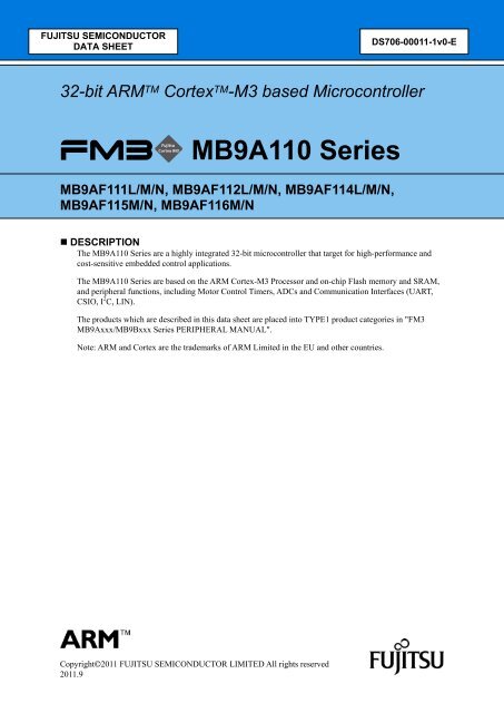
32-bit ARM TM Cortex TM -M3 based Microcontroller<br />
<strong>MB9A110</strong> <strong>Series</strong><br />
MB9AF111L/M/N, MB9AF112L/M/N, MB9AF114L/M/N,<br />
MB9AF115M/N, MB9AF116M/N<br />
DESCRIPTION<br />
The <strong>MB9A110</strong> <strong>Series</strong> are a highly integrated 32-bit microcontroller that target for high-performance and<br />
cost-sensitive embedded control applications.<br />
The <strong>MB9A110</strong> <strong>Series</strong> are based on the ARM Cortex-M3 Processor and on-chip Flash memory and SRAM,<br />
and peripheral functions, including Motor Control Timers, ADCs and Communication Interfaces (UART,<br />
CSIO, I 2 C, LIN).<br />
The products which are described in this data sheet are placed into TYPE1 product categories in "FM3<br />
MB9Axxx/MB9Bxxx <strong>Series</strong> PERIPHERAL MANUAL".<br />
Note: ARM and Cortex are the trademarks of ARM Limited in the EU and other countries.
<strong>MB9A110</strong> <strong>Series</strong><br />
FEATURES<br />
2<br />
32-bit ARM Cortex-M3 Core<br />
Processor version: r2p1<br />
Up to 40MHz Frequency Operation<br />
Integrated Nested Vectored Interrupt Controller (NVIC): 1 NMI (non-maskable interrupt) and 48<br />
peripheral interrupts and 16 priority levels<br />
24-bit System timer (Sys Tick): System timer for OS task management<br />
On-chip Memories<br />
[Flash memory]<br />
Up to 512 Kbyte<br />
Read cycle: 0wait-cycle<br />
Security function for code protection<br />
[SRAM]<br />
This <strong>Series</strong> contain a total of up to 32Kbyte on-chip SRAM memories. This is composed of two<br />
independent SRAM (SRAM0, SRAM1). SRAM0 is connected to I-code bus or D-code bus of Cortex-M3<br />
core. SRAM1 is connected to System bus.<br />
SRAM0: Up to 16 Kbyte.<br />
SRAM1: Up to 16 Kbyte.<br />
External Bus Interface*<br />
Supports SRAM, NOR Flash device<br />
Up to 8 chip selects<br />
8/16-bit Data width<br />
Up to 25-bit Address bit<br />
Supports Address/Data multiplex<br />
Supports external RDY input.<br />
* : MB9AF111L, F112L, F114L do not support External Bus Interface<br />
DS706-00011-1v0-E
DS706-00011-1v0-E<br />
<strong>MB9A110</strong> <strong>Series</strong><br />
Multi-function Serial Interface (Max 8channels)<br />
4 channels with 16-byte FIFO (ch.4-ch.7), 4 channels without FIFO (ch.0-ch.3)<br />
Operation mode is selectable from the followings for each channel.<br />
UART<br />
CSIO<br />
LIN<br />
I 2 C<br />
[UART]<br />
Full-duplex double buffer<br />
Selection with or without parity supported<br />
Built-in dedicated baud rate generator<br />
External clock available as a serial clock<br />
Hardware Flow control : Automatically control the transmission by CTS/RTS (only ch.4)*<br />
Various error detect functions available (parity errors, framing errors, and overrun errors)<br />
* : MB9AF111L, F112L, F114L do not support Hardware Flow control<br />
[CSIO]<br />
Full-duplex double buffer<br />
Built-in dedicated baud rate generator<br />
Overrun error detect function available<br />
[LIN]<br />
LIN protocol Rev.2.1 supported<br />
Full-duplex double buffer<br />
Master/Slave mode supported<br />
LIN break field generate (can be changed 13-16bit length)<br />
LIN break delimiter generate (can be changed 1-4bit length)<br />
Various error detect functions available (parity errors, framing errors, and overrun errors)<br />
[I 2 C]<br />
Standard mode (Max 100kbps) / High-speed mode (Max 400Kbps) supported<br />
DMA Controller (8channels)<br />
DMA Controller has an independent bus for CPU, so CPU and DMA Controller can process simultaneously.<br />
8 independently configured and operated channels<br />
Transfer can be started by software or request from the built-in peripherals<br />
Transfer address area: 32bit (4Gbyte)<br />
Transfer mode: Block transfer/Burst transfer/Demand transfer<br />
Transfer data type: byte/half-word/word<br />
Transfer block count: 1 to 16<br />
Number of transfers: 1 to 65536<br />
A/D Converter (Max 16channels)<br />
[12-bit A/D Converter]<br />
Successive Approximation Register type<br />
Built-in 3unit*<br />
Conversion time: 1.0μs@5V<br />
Priority conversion available (priority at 2levels)<br />
Scanning conversion mode<br />
Built-in FIFO for conversion data storage (for SCAN conversion: 16steps, for Priority conversion:<br />
4steps)<br />
* : MB9AF111L, F112L, F114L built-in 2unit<br />
3
<strong>MB9A110</strong> <strong>Series</strong><br />
4<br />
Base Timer (Max 8channels)<br />
Operation mode is selectable from the followings for each channel.<br />
16-bit PWM timer<br />
16-bit PPG timer<br />
16/32-bit reload timer<br />
16/32-bit PWC timer<br />
General Purpose I/O Port<br />
This series can use its pins as I/O ports when they are not used for external bus or peripherals. Moreover,<br />
the port relocate function is built in. It can set which I/O port the peripheral function can be allocated.<br />
Capable of pull-up control per pin<br />
Capable of reading pin level directly<br />
Built-in the port relocate function<br />
Up to 83 fast I/O Ports@100pin Package<br />
Some pins are 5V tolerant I/O (MB9AF115M/N, MB9AF116M/N only)<br />
Please see " PIN DESCRIPTION" to confirm the corresponding pins.<br />
Multi-function Timer (Max 2unit)<br />
The Multi-function timer is composed of the following blocks.<br />
16-bit free-run timer × 3ch/unit<br />
Input capture × 4ch/unit<br />
Output compare × 6ch/unit<br />
A/D activating compare × 3ch/unit<br />
Waveform generator × 3ch/unit<br />
16-bit PPG timer × 3ch/unit<br />
The following function can be used to achieve the motor control.<br />
PWM signal output function<br />
DC chopper waveform output function<br />
Dead time function<br />
Input capture function<br />
A/D convertor activate function<br />
DTIF (Motor emergency stop) interrupt function<br />
Quadrature Position/Revolution Counter (QPRC) (Max 2unit)<br />
The Quadrature Position/Revolution Counter (QPRC) is used to measure the position of the position<br />
encoder. Moreover, it is possible to use up/down counter.<br />
The detection edge of the three external event input pins AIN, BIN and ZIN is configurable.<br />
16-bit position counter<br />
16-bit revolution counter<br />
Two 16-bit compare registers<br />
Dual Timer (Two 32/16bit Down Counter)<br />
The Dual Timer consists of two programmable 32/16-bit down counters.<br />
Operation mode is selectable from the followings for each channel.<br />
Free-running<br />
Periodic (=Reload)<br />
One-shot<br />
DS706-00011-1v0-E
Watch Counter<br />
The Watch counter is used for wake up from power saving mode.<br />
Interval timer: up to 64s (Max)@ Sub Clock : 32.768kHz<br />
External Interrupt Controller Unit<br />
Up to 16 external vectors<br />
Include one non-maskable interrupt (NMI)<br />
Watch dog Timer (2channels)<br />
A watchdog timer can generate interrupts or a reset when a time-out value is reached.<br />
DS706-00011-1v0-E<br />
<strong>MB9A110</strong> <strong>Series</strong><br />
This series consists of two different watchdogs, a "Hardware" watchdog and a "Software" watchdog.<br />
"Hardware" watchdog timer is clocked by low speed CR oscillator. Therefore, "Hardware" watchdog is<br />
active in any power saving mode except STOP.<br />
CRC (Cyclic Redundancy Check) Accelerator<br />
The CRC accelerator helps a verify data transmission or storage integrity.<br />
CCITT CRC16 and IEEE-802.3 CRC32 are supported.<br />
CCITT CRC16 Generator Polynomial: 0x1021<br />
IEEE-802.3 CRC32 Generator Polynomial: 0x04C11DB7<br />
Clock and Reset<br />
[Clocks]<br />
Five clock sources (2 ext. osc, 2 CR osc, and main PLL) that are dynamically selectable.<br />
Main Clock : 4MHz to 48MHz<br />
Sub Clock : 32.768kHz<br />
High-speed CR Clock : 4MHz<br />
Low-speed CR Clock : 100kHz<br />
Main PLL Clock<br />
[Resets]<br />
Reset requests from INITX pins, Power on reset, Software reset, watchdog timers reset, low voltage<br />
detector reset and clock supervisor reset.<br />
Clock Super Visor (CSV)<br />
Clocks generated by CR oscillators are used to supervise abnormality of the external clocks.<br />
External OSC clock failure (clock stop) is detected, reset is asserted.<br />
External OSC frequency anomaly is detected, interrupt or reset is asserted.<br />
Low Voltage Detector (LVD)<br />
This <strong>Series</strong> include 2-stage monitoring of voltage on the VCC. When the voltage falls below the voltage has<br />
been set, Low Voltage Detector generates an interrupt or reset.<br />
LVD1: error reporting via interrupt<br />
LVD2: auto-reset operation<br />
5
<strong>MB9A110</strong> <strong>Series</strong><br />
6<br />
Low Power Mode<br />
Three power saving modes supported.<br />
SLEEP<br />
TIMER<br />
STOP<br />
Debug<br />
Serial Wire JTAG Debug Port (SWJ-DP)<br />
Embedded Trace Macrocells (ETM) provide comprehensive debug and trace facilities.*<br />
Trace Port Interface Unit (TPIU) for bridging to a Trace Port Analyzer.*<br />
* : MB9AF111L/M, F112L/M, F114L/M, F115M, F116M support only SWJ-DP.<br />
Power Supply<br />
VCC = 2.7V to 5.5V: Correspond to the wide range voltage.<br />
DS706-00011-1v0-E
PRODUCT LINEUP<br />
Memory size<br />
Product device MB9AF111L/M/N MB9AF112L/M/N MB9AF114L/M/N<br />
On-chip Flash 64Kbyte 128Kbyte 256Kbyte<br />
On-chip SRAM 16Kbyte 16Kbyte 32Kbyte<br />
Product device MB9AF115M/N MB9AF116M/N<br />
On-chip Flash 384Kbyte 512Kbyte<br />
On-chip SRAM 32Kbyte 32Kbyte<br />
Function<br />
Product device<br />
DS706-00011-1v0-E<br />
MB9AF111L<br />
MB9AF112L<br />
MB9AF114L<br />
<strong>MB9A110</strong> <strong>Series</strong><br />
MB9AF111M<br />
MB9AF112M<br />
MB9AF114M<br />
MB9AF115M<br />
MB9AF116M<br />
MB9AF111N<br />
MB9AF112N<br />
MB9AF114N<br />
MB9AF115N<br />
MB9AF116N<br />
Pin count 64 80 100<br />
CPU<br />
Freq.<br />
Cortex-M3<br />
40MHz<br />
Power supply voltage range 2.7V to 5.5V<br />
DMAC 8ch<br />
Addr:21bit (Max) Addr:25bit (Max)<br />
Data:8 bit<br />
Data:8/16 bit<br />
External Bus Interface -<br />
CS:4 (Max)<br />
CS:8 (Max)<br />
Support: SRAM, Support: SRAM,<br />
NOR Flash<br />
NOR Flash<br />
MF Serial Interface<br />
(UART/CSIO/LIN/I 2 C)<br />
8ch (Max)<br />
Base Timer<br />
(PWC/Reload timer/PWM/PPG)<br />
A/D<br />
8ch (Max)<br />
activation<br />
compare<br />
3ch<br />
Input<br />
capture<br />
4ch<br />
MF-<br />
Timer<br />
Free-run<br />
timer<br />
3ch<br />
1 unit 2 units (Max)<br />
Output<br />
compare<br />
6ch<br />
Waveform<br />
generator<br />
3ch<br />
PPG 3ch<br />
QPRC 2ch (Max)<br />
Dual Timer 1 unit<br />
Watch Counter 1 unit<br />
CRC Accelerator Yes<br />
Watchdog timer 1ch (SW) + 1ch (HW)<br />
External Interrupts 7pins (Max) + NMI × 1 11pins (Max) + NMI × 1 16pins (Max) + NMI × 1<br />
I/O ports 51pins (Max) 66pins (Max) 83pins (Max)<br />
12 bit A/D converter 9ch (2 units) 12ch (3 units) 16ch (3 units)<br />
CSV (Clock Super Visor) Yes<br />
LVD (Low Voltage Detector) 2ch<br />
Internal High-speed 4MHz (± 2%)<br />
OSC Low-speed 100kHz (Typ)<br />
Debug Function SWJ-DP SWJ-DP/TPIU/ETM<br />
7
<strong>MB9A110</strong> <strong>Series</strong><br />
Note: All signals of the peripheral function in each product cannot be allocated by limiting the pins of package.<br />
It is necessary to use the port relocate function of the General I/O port according to your function use.<br />
8<br />
DS706-00011-1v0-E
PACKAGES<br />
Package<br />
DS706-00011-1v0-E<br />
Product name<br />
MB9AF111L<br />
MB9AF112L<br />
MB9AF114L<br />
<strong>MB9A110</strong> <strong>Series</strong><br />
MB9AF111M<br />
MB9AF112M<br />
MB9AF114M<br />
MB9AF115M<br />
MB9AF116M<br />
MB9AF111N<br />
MB9AF112N<br />
MB9AF114N<br />
MB9AF115N<br />
MB9AF116N<br />
LQFP: FPT-64P-M24/M38 (0.5mm pitch) - -<br />
LQFP: FPT-64P-M23/M39 (0.65mm pitch) - -<br />
LQFP: FPT-80P-M21/M37 (0.5mm pitch) - -<br />
LQFP: FPT-100P-M20/M23 (0.5mm pitch) - - <br />
QFP: FPT-100P-M06 (0.65mm pitch) - - <br />
BGA: BGA-112P-M04 (0.8mm pitch) - - *<br />
: Supported<br />
* : MB9AF115N, MB9AF116N is planning<br />
Note : Refer to "PACKAGE DIMENSIONS" for detailed information on each package.<br />
9
<strong>MB9A110</strong> <strong>Series</strong><br />
PIN ASSIGNMENT<br />
FPT-100P-M20/M23<br />
10<br />
(TOP VIEW)<br />
<br />
The number after the underscore ("_") in pin names such as XXX_1 and XXX_2 indicates the relocated<br />
port number. For these pins, there are multiple pins that provide the same function for the same channel.<br />
Use the extended port function register (EPFR) to select the pin.<br />
DS706-00011-1v0-E
FPT-100P-M06<br />
DS706-00011-1v0-E<br />
(TOP VIEW)<br />
<strong>MB9A110</strong> <strong>Series</strong><br />
<br />
The number after the underscore ("_") in pin names such as XXX_1 and XXX_2 indicates the relocated<br />
port number. For these pins, there are multiple pins that provide the same function for the same channel.<br />
Use the extended port function register (EPFR) to select the pin.<br />
11
<strong>MB9A110</strong> <strong>Series</strong><br />
FPT-80P-M21/FPT-80P-M37<br />
12<br />
(TOP VIEW)<br />
<br />
The number after the underscore ("_") in pin names such as XXX_1 and XXX_2 indicates the relocated<br />
port number. For these pins, there are multiple pins that provide the same function for the same channel.<br />
Use the extended port function register (EPFR) to select the pin.<br />
DS706-00011-1v0-E
FPT-64P-M23/M24/M38/M39<br />
DS706-00011-1v0-E<br />
(TOP VIEW)<br />
<strong>MB9A110</strong> <strong>Series</strong><br />
<br />
The number after the underscore ("_") in pin names such as XXX_1 and XXX_2 indicates the relocated<br />
port number. For these pins, there are multiple pins that provide the same function for the same channel.<br />
Use the extended port function register (EPFR) to select the pin.<br />
13
<strong>MB9A110</strong> <strong>Series</strong><br />
BGA-112P-M04<br />
14<br />
A<br />
B<br />
C<br />
D<br />
E<br />
F<br />
G<br />
H<br />
J<br />
K<br />
L<br />
1 2<br />
VSS<br />
VCC<br />
P50<br />
P53<br />
P30<br />
P34<br />
P37<br />
P3B<br />
VCC<br />
VCC<br />
VSS<br />
VSS<br />
P3F<br />
3 4 5<br />
P81 P80 VCC P0E<br />
P51<br />
P54<br />
P31<br />
P35<br />
P38<br />
VSS P40<br />
VSS X1A INITX<br />
(TOP VIEW)<br />
6 7<br />
P0B P07<br />
P52 P61 P0F P0C P08<br />
VSS<br />
P55<br />
P32<br />
P36<br />
VSS<br />
P33<br />
P39<br />
P3A P3D<br />
P3C P3E VSS<br />
P60 P62<br />
P56 P63<br />
Index<br />
8 9 10<br />
TMS/<br />
SWDIO<br />
P22<br />
AN13<br />
P44 P4C AN05 VSS<br />
P43 P49<br />
P42<br />
P0D<br />
P09<br />
P0A<br />
P48 P4B<br />
TDO/<br />
SWO<br />
P05<br />
VSS<br />
AN08<br />
TRSTX<br />
TCK/<br />
SWCLK<br />
VSS<br />
P06<br />
AN14<br />
AN10<br />
AN07<br />
AN04<br />
P4D AN02 VSS<br />
P4E MD1<br />
VCC<br />
VSS<br />
P20<br />
P23<br />
AN12<br />
AN09<br />
AN06<br />
AN03<br />
AN01<br />
VSS<br />
11<br />
VSS<br />
C X0A VSS P41 P45 P4A MD0 X0 X1 VSS<br />
TDI<br />
P21<br />
AN15<br />
AN11<br />
AVRH<br />
AVSS<br />
AVCC<br />
AN00<br />
<br />
The number after the underscore ("_") in pin names such as XXX_1 and XXX_2 indicates the relocated<br />
port number. For these pins, there are multiple pins that provide the same function for the same channel.<br />
Use the extended port function register (EPFR) to select the pin.<br />
VCC<br />
DS706-00011-1v0-E
DS706-00011-1v0-E<br />
<strong>MB9A110</strong> <strong>Series</strong><br />
PIN DESCRIPTION<br />
Pin No<br />
LQFP-100 QFP-100 BGA-112 LQFP-80 LQFP-64<br />
Pin name<br />
I/O circuit<br />
type<br />
Pin state<br />
type<br />
1 79 B1 1 1 VCC<br />
P50<br />
-<br />
2<br />
INT00_0<br />
AIN0_2<br />
2 80 C1 2<br />
SIN3_1<br />
RTO10_0<br />
E H<br />
- (PPG10_0)<br />
MADATA00_1<br />
P51<br />
INT01_0<br />
3 BIN0_2<br />
3 81 C2 3<br />
SOT3_1<br />
(SDA3_1)<br />
RTO11_0<br />
E H<br />
- (PPG10_0)<br />
MADATA01_1<br />
P52<br />
INT02_0<br />
4 ZIN0_2<br />
4 82 B3 4<br />
SCK3_1<br />
(SCL3_1)<br />
RTO12_0<br />
E H<br />
- (PPG12_0)<br />
MADATA02_1<br />
P53<br />
SIN6_0<br />
TIOA1_2<br />
5 83 D1 5 - INT07_2<br />
RTO13_0<br />
(PPG12_0)<br />
MADATA03_1<br />
P54<br />
SOT6_0<br />
(SDA6_0)<br />
E H<br />
6 84 D2 6 - TIOB1_2<br />
RTO14_0<br />
(PPG14_0)<br />
MADATA04_1<br />
E I<br />
15
<strong>MB9A110</strong> <strong>Series</strong><br />
Pin No<br />
LQFP-100 QFP-100 BGA-112 LQFP-80 LQFP-64<br />
Pin name<br />
P55<br />
SCK6_0<br />
(SCL6_0)<br />
7 85 D3 7 - ADTG_1<br />
RTO15_0<br />
(PPG14_0)<br />
MADATA05_1<br />
P56<br />
8 86 D5 8 -<br />
INT08_2<br />
DTTI1X_0<br />
MADATA06_1<br />
P30<br />
9 87 E1 9<br />
5<br />
AIN0_0<br />
TIOB0_1<br />
INT03_2<br />
- MADATA07_1<br />
P31<br />
BIN0_0<br />
10 88 E2 10<br />
6<br />
TIOB1_1<br />
SCK6_1<br />
(SCL6_1)<br />
INT04_2<br />
- MADATA08_1<br />
P32<br />
ZIN0_0<br />
11 89 E3 11<br />
7<br />
TIOB2_1<br />
SOT6_1<br />
(SDA6_1)<br />
INT05_2<br />
- MADATA09_1<br />
P33<br />
INT04_0<br />
12 90 E4 12<br />
8 TIOB3_1<br />
SIN6_1<br />
ADTG_6<br />
- MADATA10_1<br />
P34<br />
13 91 F1 - -<br />
FRCK0_0<br />
TIOB4_1<br />
MADATA11_1<br />
16<br />
I/O circuit<br />
type<br />
Pin state<br />
type<br />
E I<br />
E H<br />
E H<br />
E H<br />
E H<br />
E H<br />
E I<br />
DS706-00011-1v0-E
Pin No<br />
LQFP-100 QFP-100 BGA-112 LQFP-80 LQFP-64<br />
DS706-00011-1v0-E<br />
<strong>MB9A110</strong> <strong>Series</strong><br />
Pin name<br />
I/O circuit<br />
type<br />
Pin state<br />
type<br />
14 92 F2 - -<br />
P35<br />
IC03_0<br />
TIOB5_1<br />
INT08_1<br />
MADATA12_1<br />
P36<br />
IC02_0<br />
E H<br />
15 93 F3 - -<br />
SIN5_2<br />
INT09_1<br />
MADATA13_1<br />
P37<br />
IC01_0<br />
E H<br />
16 94 G1 - -<br />
SOT5_2<br />
(SDA5_2)<br />
INT10_1<br />
MADATA14_1<br />
P38<br />
IC00_0<br />
E H<br />
17 95 G2 - -<br />
SCK5_2<br />
(SCL5_2)<br />
INT11_1<br />
MADATA15_1<br />
P39<br />
E H<br />
18 96 F4 13 9 DTTI0X_0<br />
ADTG_2<br />
P3A<br />
E I<br />
19 97 G3 14 10<br />
RTO00_0<br />
(PPG00_0)<br />
TIOA0_1<br />
P3B<br />
G I<br />
20 98 H1 15 11<br />
RTO01_0<br />
(PPG00_0)<br />
TIOA1_1<br />
P3C<br />
G I<br />
21 99 H2 16 12<br />
RTO02_0<br />
(PPG02_0)<br />
TIOA2_1<br />
P3D<br />
G I<br />
22 100 G4 17 13<br />
RTO03_0<br />
(PPG02_0)<br />
TIOA3_1<br />
G I<br />
- - B2 - - VSS -<br />
17
<strong>MB9A110</strong> <strong>Series</strong><br />
Pin No<br />
LQFP-100 QFP-100 BGA-112 LQFP-80 LQFP-64<br />
18<br />
Pin name<br />
I/O circuit<br />
type<br />
Pin state<br />
type<br />
23 1 H3 18 14<br />
P3E<br />
RTO04_0<br />
(PPG04_0)<br />
TIOA4_1<br />
P3F<br />
G I<br />
24 2 J2 19 15<br />
RTO05_0<br />
(PPG04_0)<br />
TIOA5_1<br />
G I<br />
25 3 L1 20 16 VSS -<br />
26 4 J1 - - VCC<br />
P40<br />
TIOA0_0<br />
-<br />
27 5 J4 - - RTO10_1<br />
(PPG10_1)<br />
INT12_1<br />
P41<br />
TIOA1_0<br />
G H<br />
28 6 L5 - - RTO11_1<br />
(PPG10_1)<br />
INT13_1<br />
P42<br />
G H<br />
29 7 K5 - -<br />
TIOA2_0<br />
RTO12_1<br />
(PPG12_1)<br />
P43<br />
TIOA3_0<br />
G I<br />
30 8 J5 - - RTO13_1<br />
(PPG12_1)<br />
ADTG_7<br />
P44<br />
G I<br />
21<br />
TIOA4_0<br />
31 9 H5<br />
- MAD00_1 G I<br />
-<br />
RTO14_1<br />
(PPG14_1)<br />
P45<br />
22<br />
TIOA5_0<br />
32 10 L6<br />
- MAD01_1 G I<br />
-<br />
RTO15_1<br />
(PPG14_1)<br />
- - K2 - - VSS -<br />
- - J3 - - VSS -<br />
- - H4 - - VSS -<br />
DS706-00011-1v0-E
DS706-00011-1v0-E<br />
<strong>MB9A110</strong> <strong>Series</strong><br />
Pin No<br />
LQFP-100 QFP-100 BGA-112 LQFP-80 LQFP-64<br />
Pin name<br />
I/O circuit<br />
type<br />
Pin state<br />
type<br />
33 11 L2 23 17 C -<br />
34 12 L4 24 - VSS -<br />
35 13 K1 25 18 VCC -<br />
36 14 L3 26 19<br />
P46<br />
X0A<br />
D M<br />
37 15 K3 27 20<br />
P47<br />
X1A<br />
D N<br />
38 16 K4 28 21 INITX<br />
P48<br />
DTTI1X_1<br />
B C<br />
39 17 K6 29 - INT14_1<br />
SIN3_2<br />
MAD02_1<br />
P49<br />
E H<br />
22 TIOB0_0<br />
AIN0_1<br />
40 18 J6 30<br />
IC10_1 E I<br />
-<br />
SOT3_2<br />
(SDA3_2)<br />
MAD03_1<br />
P4A<br />
23 TIOB1_0<br />
BIN0_1<br />
41 19 L7 31<br />
IC11_1 E I<br />
-<br />
SCK3_2<br />
(SCL3_2)<br />
MAD04_1<br />
P4B<br />
24 TIOB2_0<br />
42 20 K7 32<br />
ZIN0_1 E I<br />
-<br />
IC12_1<br />
MAD05_1<br />
P4C<br />
TIOB3_0<br />
25 SCK7_1<br />
43 21 H6 33<br />
(SCL7_1)<br />
AIN1_2<br />
E / I* I<br />
-<br />
IC13_1<br />
MAD06_1<br />
19
<strong>MB9A110</strong> <strong>Series</strong><br />
Pin No<br />
LQFP-100 QFP-100 BGA-112 LQFP-80 LQFP-64<br />
Pin name<br />
P4D<br />
TIOB4_0<br />
I/O circuit<br />
type<br />
Pin state<br />
type<br />
26 SOT7_1<br />
44 22 J7 34<br />
(SDA7_1)<br />
BIN1_2<br />
E / I* I<br />
-<br />
FRCK1_1<br />
MAD07_1<br />
P4E<br />
TIOB5_0<br />
45 23 K8 35<br />
27 INT06_2<br />
SIN7_1<br />
ZIN1_2<br />
E / I* I<br />
- MAD08_1<br />
46 24 K9 36 28<br />
MD1<br />
PE0<br />
C P<br />
47 25 L8 37 29 MD0 J D<br />
48 26 L9 38 30<br />
X0<br />
PE2<br />
A A<br />
49 27 L10 39 31<br />
X1<br />
PE3<br />
A B<br />
50 28 L11 40 32 VSS -<br />
51 29 K11 41 33 VCC -<br />
52 30 J11 42 34<br />
P10<br />
AN00<br />
P11<br />
AN01<br />
F K<br />
53 31 J10 43<br />
35 SIN1_1<br />
INT02_1<br />
FRCK0_2<br />
F L<br />
- MAD09_1<br />
P12<br />
AN02<br />
54 32 J8 44<br />
36 SOT1_1<br />
(SDA1_1)<br />
IC00_2<br />
F K<br />
- MAD10_1<br />
- - K10 - - VSS -<br />
- - J9 - - VSS -<br />
20<br />
DS706-00011-1v0-E
DS706-00011-1v0-E<br />
<strong>MB9A110</strong> <strong>Series</strong><br />
Pin No<br />
LQFP-100 QFP-100 BGA-112 LQFP-80 LQFP-64<br />
Pin name<br />
P13<br />
AN03<br />
I/O circuit<br />
type<br />
Pin state<br />
type<br />
55 33 H10 45<br />
37 SCK1_1<br />
(SCL1_1)<br />
IC01_2<br />
F K<br />
- MAD11_1<br />
P14<br />
56 34 H9 46<br />
38<br />
AN04<br />
INT03_1<br />
IC02_2<br />
F L<br />
-<br />
SIN0_1<br />
MAD12_1<br />
P15<br />
39<br />
AN05<br />
57 35 H7 47<br />
IC03_2<br />
SOT0_1<br />
F K<br />
- (SDA0_1)<br />
MAD13_1<br />
P16<br />
AN06<br />
58 36 G10 48 - SCK0_1<br />
(SCL0_1)<br />
MAD14_1<br />
P17<br />
F K<br />
59 37 G9 49<br />
40<br />
AN07<br />
SIN2_2<br />
INT04_1<br />
F L<br />
- MAD15_1<br />
60 38 H11 50 41 AVCC -<br />
61 39 F11 51 42 AVRH -<br />
62 40 G11 52 43 AVSS<br />
P18<br />
-<br />
63 41 G8 53<br />
44<br />
AN08<br />
SOT2_2<br />
(SDA2_2)<br />
F K<br />
- MAD16_1<br />
P19<br />
64 42 F10 54<br />
45<br />
AN09<br />
SCK2_2<br />
(SCL2_2)<br />
F K<br />
- MAD17_1<br />
- - H8 - - VSS -<br />
21
<strong>MB9A110</strong> <strong>Series</strong><br />
Pin No<br />
LQFP-100 QFP-100 BGA-112 LQFP-80 LQFP-64<br />
22<br />
Pin name<br />
I/O circuit<br />
type<br />
Pin state<br />
type<br />
65 43 F9 55 -<br />
P1A<br />
AN10<br />
SIN4_1<br />
INT05_1<br />
IC00_1<br />
MAD18_1<br />
P1B<br />
AN11<br />
F L<br />
66 44 E11 56 -<br />
SOT4_1<br />
(SDA4_1)<br />
IC01_1<br />
MAD19_1<br />
P1C<br />
AN12<br />
F K<br />
67 45 E10 - -<br />
SCK4_1<br />
(SCL4_1)<br />
IC02_1<br />
MAD20_1<br />
P1D<br />
AN13<br />
F K<br />
68 46 F8 - - CTS4_1<br />
IC03_1<br />
MAD21_1<br />
P1E<br />
AN14<br />
F K<br />
69 47 E9 - - RTS4_1<br />
DTTI0X_1<br />
MAD22_1<br />
P1F<br />
AN15<br />
F K<br />
70 48 D11 - - ADTG_5<br />
FRCK0_1<br />
MAD23_1<br />
F K<br />
- - B10 - - VSS -<br />
- - C9 - - VSS -<br />
DS706-00011-1v0-E
DS706-00011-1v0-E<br />
<strong>MB9A110</strong> <strong>Series</strong><br />
Pin No<br />
LQFP-100 QFP-100 BGA-112 LQFP-80 LQFP-64<br />
Pin name<br />
P23<br />
I/O circuit<br />
type<br />
Pin state<br />
type<br />
71 49 D10<br />
57 46<br />
SCK0_0<br />
(SCL0_0)<br />
TIOA7_1<br />
E I<br />
- -<br />
RTO00_1<br />
(PPG00_1)<br />
P22<br />
72 50 E8 58<br />
47<br />
SOT0_0<br />
(SDA0_0)<br />
TIOB7_1<br />
E I<br />
- ZIN1_1<br />
P21<br />
73 51 C11 59<br />
48 SIN0_0<br />
INT06_1<br />
E H<br />
- BIN1_1<br />
P20<br />
INT05_0<br />
74 52 C10 60 - CROUT_0<br />
AIN1_1<br />
MAD24_1<br />
E H<br />
75 53 A11 - - VSS -<br />
76 54 A10 - - VCC -<br />
77 55 A9 61<br />
49<br />
P00<br />
TRSTX E E<br />
- MCSX7_1<br />
P01<br />
78 56 B9 62 50<br />
TCK<br />
SWCLK<br />
E E<br />
79 57 B11 63<br />
51<br />
P02<br />
TDI<br />
E E<br />
- MCSX6_1<br />
P03<br />
80 58 A8 64 52<br />
TMS<br />
SWDIO<br />
P04<br />
E E<br />
81 59 B8 65 53<br />
TDO<br />
SWO<br />
P05<br />
TRACED0<br />
E E<br />
82 60 C8 - -<br />
TIOA5_2<br />
SIN4_2<br />
INT00_1<br />
MCSX5_1<br />
E F<br />
- - D8 - - VSS -<br />
23
<strong>MB9A110</strong> <strong>Series</strong><br />
Pin No<br />
LQFP-100 QFP-100 BGA-112 LQFP-80 LQFP-64<br />
24<br />
Pin name<br />
I/O circuit<br />
type<br />
Pin state<br />
type<br />
83 61 D9 - -<br />
P06<br />
TRACED1<br />
TIOB5_2<br />
SOT4_2<br />
(SDA4_2)<br />
INT01_1<br />
MCSX4_1<br />
P07<br />
E F<br />
66<br />
ADTG_0<br />
84 62 A7<br />
-<br />
MCLKOUT_1<br />
TRACED2<br />
E G<br />
-<br />
SCK4_2<br />
(SCL4_2)<br />
P08<br />
TRACED3<br />
85 63 B7 - - TIOA0_2<br />
CTS4_2<br />
MCSX3_1<br />
P09<br />
TRACECLK<br />
E G<br />
86 64 C7 - - TIOB0_2<br />
RTS4_2<br />
MCSX2_1<br />
P0A<br />
E G<br />
54 SIN4_0<br />
87 65 D7 67<br />
INT00_2 E / I* H<br />
-<br />
FRCK1_0<br />
MCSX1_1<br />
P0B<br />
88 66 A6 68<br />
55<br />
SOT4_0<br />
(SDA4_0)<br />
TIOB6_1<br />
E / I* I<br />
-<br />
IC10_0<br />
MCSX0_1<br />
P0C<br />
89 67 B6 69<br />
56<br />
SCK4_0<br />
(SCL4_0)<br />
TIOA6_1<br />
E / I* I<br />
-<br />
IC11_0<br />
MALE_1<br />
- - D4 - - VSS -<br />
- - C3 - - VSS -<br />
DS706-00011-1v0-E
DS706-00011-1v0-E<br />
<strong>MB9A110</strong> <strong>Series</strong><br />
Pin No<br />
LQFP-100 QFP-100 BGA-112 LQFP-80 LQFP-64<br />
Pin name<br />
P0D<br />
RTS4_0<br />
I/O circuit<br />
type<br />
Pin state<br />
type<br />
90 68 C6 70 - TIOA3_2<br />
IC12_0<br />
MDQM0_1<br />
P0E<br />
CTS4_0<br />
E I<br />
91 69 A5 71 - TIOB3_2<br />
IC13_0<br />
MDQM1_1<br />
P0F<br />
E I<br />
92 70 B5 72 57 NMIX<br />
CROUT_1<br />
P63<br />
E J<br />
93 71 D6 73 - INT03_0<br />
MWEX_1<br />
P62<br />
E H<br />
94 72 C5 74<br />
58<br />
SCK5_0<br />
(SCL5_0)<br />
ADTG_3<br />
E I<br />
- MOEX_1<br />
P61<br />
95 73 B4 75 59<br />
SOT5_0<br />
(SDA5_0)<br />
TIOB2_2<br />
P60<br />
E I<br />
96 74 C4 76<br />
60<br />
SIN5_0<br />
TIOA2_2<br />
INT15_1<br />
E / I* H<br />
- MRDY_1<br />
97 75 A4 77 61 VCC -<br />
98 76 A3 78 62 P80 H O<br />
99 77 A2 79 63 P81 H O<br />
100 78 A1 80 64 VSS -<br />
* : 5V tolerant I/O on MB9AF115M/N, MB9AF116M/N<br />
The number after the underscore ("_") in pin names such as XXX_1 and XXX_2 indicates the relocated<br />
port number. For these pins, there are multiple pins that provide the same function for the same channel.<br />
Use the extended port function register (EPFR) to select the pin.<br />
25
<strong>MB9A110</strong> <strong>Series</strong><br />
SIGNAL DESCRIPTION<br />
Module Pin name Function LQFP- QFP-<br />
Pin No<br />
BGA- LQFP- LQFP-<br />
100 100 112 80 64<br />
ADC ADTG_0 84 62 A7 66 -<br />
ADTG_1 7 85 D3 7 -<br />
ADTG_2 18 96 F4 13 9<br />
ADTG_3<br />
ADTG_4<br />
ADTG_5<br />
A/D converter external trigger input<br />
pin<br />
94<br />
-<br />
70<br />
72<br />
-<br />
48<br />
C5<br />
-<br />
D11<br />
74<br />
-<br />
-<br />
58<br />
-<br />
-<br />
ADTG_6 12 90 E4 12 8<br />
ADTG_7 30 8 J5 - -<br />
ADTG_8<br />
- - - - -<br />
AN00 52 30 J11 42 34<br />
AN01 53 31 J10 43 35<br />
AN02 54 32 J8 44 36<br />
AN03 55 33 H10 45 37<br />
AN04 56 34 H9 46 38<br />
AN05 57 35 H7 47 39<br />
AN06 58 36 G10 48 -<br />
AN07 A/D converter analog input pin 59 37 G9 49 40<br />
AN08 ANxx describes ADC ch.xx.<br />
63 41 G8 53 44<br />
AN09 64 42 F10 54 45<br />
AN10 65 43 F9 55 -<br />
AN11 66 44 E11 56 -<br />
AN12 67 45 E10 - -<br />
AN13 68 46 F8 - -<br />
AN14 69 47 E9 - -<br />
AN15<br />
70 48 D11 - -<br />
Base Timer TIOA0_0 27 5 J4 - -<br />
0 TIOA0_1 Base timer ch.0 TIOA pin<br />
19 97 G3 14 10<br />
TIOA0_2<br />
85 63 B7 - -<br />
TIOB0_0 40 18 J6 30 22<br />
TIOB0_1 Base timer ch.0 TIOB pin<br />
9 87 E1 9 5<br />
TIOB0_2<br />
86 64 C7 - -<br />
Base Timer TIOA1_0 28 6 L5 - -<br />
1 TIOA1_1 Base timer ch.1 TIOA pin<br />
20 98 H1 15 11<br />
TIOA1_2<br />
5 83 D1 5 -<br />
TIOB1_0 41 19 L7 31 23<br />
TIOB1_1 Base timer ch.1 TIOB pin<br />
10 88 E2 10 6<br />
TIOB1_2<br />
6 84 D2 6 -<br />
Base Timer TIOA2_0 29 7 K5 - -<br />
2 TIOA2_1 Base timer ch.2 TIOA pin<br />
21 99 H2 16 12<br />
TIOA2_2<br />
96 74 C4 76 60<br />
TIOB2_0 42 20 K7 32 24<br />
TIOB2_1 Base timer ch.2 TIOB pin<br />
11 89 E3 11 7<br />
TIOB2_2<br />
95 73 B4 75 59<br />
26<br />
DS706-00011-1v0-E
DS706-00011-1v0-E<br />
<strong>MB9A110</strong> <strong>Series</strong><br />
Module Pin name Function LQFP- QFP-<br />
Pin No<br />
BGA- LQFP- LQFP-<br />
100 100 112 80 64<br />
Base Timer TIOA3_0 30 8 J5 - -<br />
3 TIOA3_1 Base timer ch.3 TIOA pin<br />
22 100 G4 17 13<br />
TIOA3_2<br />
90 68 C6 70 -<br />
TIOB3_0 43 21 H6 33 25<br />
TIOB3_1 Base timer ch.3 TIOB pin<br />
12 90 E4 12 8<br />
TIOB3_2<br />
91 69 A5 71 -<br />
Base Timer TIOA4_0 31 9 H5 21 -<br />
4 TIOA4_1 Base timer ch.4 TIOA pin<br />
23 1 H3 18 14<br />
TIOA4_2<br />
- - - - -<br />
TIOB4_0 44 22 J7 34 26<br />
TIOB4_1 Base timer ch.4 TIOB pin<br />
13 91 F1 - -<br />
TIOB4_2<br />
- - - - -<br />
Base Timer TIOA5_0 32 10 L6 22 -<br />
5 TIOA5_1 Base timer ch.5 TIOA pin<br />
24 2 J2 19 15<br />
TIOA5_2<br />
82 60 C8 - -<br />
TIOB5_0 45 23 K8 35 27<br />
TIOB5_1 Base timer ch.5 TIOB pin<br />
14 92 F2 - -<br />
TIOB5_2<br />
83 61 D9 - -<br />
Base Timer TIOA6_1 Base timer ch.6 TIOA pin 89 67 B6 69 56<br />
6 TIOB6_1 Base timer ch.6 TIOB pin 88 66 A6 68 55<br />
Base Timer TIOA7_0 - - - - -<br />
7 TIOA7_1 Base timer ch.7 TIOA pin<br />
71 49 D10 57 46<br />
TIOA7_2<br />
- - - - -<br />
TIOB7_0 - - - - -<br />
TIOB7_1 Base timer ch.7 TIOB pin<br />
72 50 E8 58 47<br />
TIOB7_2<br />
- - - - -<br />
27
<strong>MB9A110</strong> <strong>Series</strong><br />
28<br />
Module Pin name Function LQFP- QFP-<br />
Pin No<br />
BGA- LQFP- LQFP-<br />
100 100 112 80 64<br />
Debugger SWCLK Serial wire debug interface clock input 78 56 B9 62 50<br />
SWDIO<br />
Serial wire debug interface data input /<br />
output<br />
80 58 A8 64 52<br />
SWO Serial wire viewer output 81 59 B8 65 53<br />
TCK J-TAG test clock input 78 56 B9 62 50<br />
TDI J-TAG test data input 79 57 B11 63 51<br />
TDO J-TAG debug data output 81 59 B8 65 53<br />
TMS J-TAG test mode state input/output 80 58 A8 64 52<br />
TRACECLK Trace CLK output of ETM 86 64 C7 - -<br />
TRACED0 82 60 C8 - -<br />
TRACED1<br />
TRACED2<br />
Trace data output of ETM<br />
83<br />
84<br />
61<br />
62<br />
D9<br />
A7<br />
-<br />
-<br />
-<br />
-<br />
TRACED3<br />
85 63 B7 - -<br />
TRSTX J-TAG test reset Input 77 55 A9 61 49<br />
External MAD00_1 31 9 H5 21 -<br />
Bus MAD01_1 32 10 L6 22 -<br />
MAD02_1 39 17 K6 29 -<br />
MAD03_1 40 18 J6 30 -<br />
MAD04_1 41 19 L7 31 -<br />
MAD05_1 42 20 K7 32 -<br />
MAD06_1 43 21 H6 33 -<br />
MAD07_1 44 22 J7 34 -<br />
MAD08_1 45 23 K8 35 -<br />
MAD09_1 53 31 J10 43 -<br />
MAD10_1 54 32 J8 44 -<br />
MAD11_1 55 33 H10 45 -<br />
MAD12_1 External bus interface address bus 56 34 H9 46 -<br />
MAD13_1 57 35 H7 47 -<br />
MAD14_1 58 36 G10 48 -<br />
MAD15_1 59 37 G9 49 -<br />
MAD16_1 63 41 G8 53 -<br />
MAD17_1 64 42 F10 54 -<br />
MAD18_1 65 43 F9 55 -<br />
MAD19_1 66 44 E11 56 -<br />
MAD20_1 67 45 E10 - -<br />
MAD21_1 68 46 F8 - -<br />
MAD22_1 69 47 E9 - -<br />
MAD23_1 70 48 D11 - -<br />
MAD24_1<br />
74 52 C10 60 -<br />
DS706-00011-1v0-E
DS706-00011-1v0-E<br />
<strong>MB9A110</strong> <strong>Series</strong><br />
Module Pin name Function LQFP- QFP-<br />
Pin No<br />
BGA- LQFP- LQFP-<br />
100 100 112 80 64<br />
External MCSX0_1 88 66 A6 68 -<br />
Bus MCSX1_1 87 65 D7 67 -<br />
MCSX2_1 86 64 C7 - -<br />
MCSX3_1<br />
MCSX4_1<br />
External bus interface chip select<br />
output pin<br />
85<br />
83<br />
63<br />
61<br />
B7<br />
D9<br />
-<br />
-<br />
-<br />
-<br />
MCSX5_1 82 60 C8 - -<br />
MCSX6_1 79 57 B11 63 -<br />
MCSX7_1<br />
77 55 A9 61 -<br />
MDQM0_1 External bus interface byte mask signal 90 68 C6 70 -<br />
MDQM1_1 output 91 69 A5 71 -<br />
MOEX_1<br />
External bus interface read enable<br />
signal for SRAM<br />
94 72 C5 74 -<br />
MWEX_1<br />
External bus interface write enable<br />
signal for SRAM<br />
93 71 D6 73 -<br />
MADATA00_1 2 80 C1 2 -<br />
MADATA01_1 3 81 C2 3 -<br />
MADATA02_1 4 82 B3 4 -<br />
MADATA03_1 5 83 D1 5 -<br />
MADATA04_1 6 84 D2 6 -<br />
MADATA05_1 7 85 D3 7 -<br />
MADATA06_1 8 86 D5 8 -<br />
MADATA07_1<br />
MADATA08_1<br />
External bus interface data bus<br />
9<br />
10<br />
87<br />
88<br />
E1<br />
E2<br />
9<br />
10<br />
-<br />
-<br />
MADATA09_1 11 89 E3 11 -<br />
MADATA10_1 12 90 E4 12 -<br />
MADATA11_1 13 91 F1 - -<br />
MADATA12_1 14 92 F2 - -<br />
MADATA13_1 15 93 F3 - -<br />
MADATA14_1 16 94 G1 - -<br />
MADATA15_1<br />
17 95 G2 - -<br />
MALE_1<br />
External bus interface Address Latch<br />
enable output signal for multiplex<br />
89 67 B6 69 -<br />
MRDY_1<br />
External bus interface external RDY<br />
input signal<br />
96 74 C4 76 -<br />
External bus interface external clock<br />
MCLKOUT_1<br />
output<br />
84 62 A7 66 -<br />
29
<strong>MB9A110</strong> <strong>Series</strong><br />
30<br />
Module Pin name Function LQFP- QFP-<br />
Pin No<br />
BGA- LQFP- LQFP-<br />
100 100 112 80 64<br />
External<br />
Interrupt<br />
INT00_0<br />
INT00_1<br />
INT00_2<br />
External interrupt request 00<br />
input pin<br />
2<br />
82<br />
87<br />
80<br />
60<br />
65<br />
C1<br />
C8<br />
D7<br />
2<br />
-<br />
67<br />
2<br />
-<br />
54<br />
INT01_0 External interrupt request 01<br />
3 81 C2 3 3<br />
INT01_1 input pin 83 61 D9 - -<br />
INT02_0 External interrupt request 02<br />
4 82 B3 4 4<br />
INT02_1 input pin 53 31 J10 43 35<br />
INT03_0<br />
INT03_1<br />
INT03_2<br />
External interrupt request 03<br />
input pin<br />
93<br />
56<br />
9<br />
71<br />
34<br />
87<br />
D6<br />
H9<br />
E1<br />
73<br />
46<br />
9<br />
-<br />
38<br />
5<br />
INT04_0<br />
INT04_1<br />
INT04_2<br />
External interrupt request 04<br />
input pin<br />
12<br />
59<br />
10<br />
90<br />
37<br />
88<br />
E4<br />
G9<br />
E2<br />
12<br />
49<br />
10<br />
8<br />
40<br />
6<br />
INT05_0<br />
INT05_1<br />
INT05_2<br />
External interrupt request 05<br />
input pin<br />
74<br />
65<br />
11<br />
52<br />
43<br />
89<br />
C10<br />
F9<br />
E3<br />
60<br />
55<br />
11<br />
-<br />
-<br />
7<br />
INT06_1 External interrupt request 06<br />
73 51 C11 59 48<br />
INT06_2 input pin 45 23 K8 35 27<br />
INT07_2<br />
External interrupt request 07<br />
input pin<br />
5 83 D1 5 -<br />
INT08_1 External interrupt request 08<br />
14 92 F2 - -<br />
INT08_2 input pin 8 86 D5 8 -<br />
INT09_1<br />
External interrupt request 09<br />
input pin<br />
15 93 F3 - -<br />
INT10_1<br />
External interrupt request 10<br />
input pin<br />
16 94 G1 - -<br />
INT11_1<br />
External interrupt request 11<br />
input pin<br />
17 95 G2 - -<br />
INT12_1<br />
External interrupt request 12<br />
input pin<br />
27 5 J4 - -<br />
INT13_1<br />
External interrupt request 13<br />
input pin<br />
28 6 L5 - -<br />
INT14_1<br />
External interrupt request 14<br />
input pin<br />
39 17 K6 29 -<br />
INT15_1<br />
External interrupt request 15<br />
input pin<br />
96 74 C4 76 60<br />
NMIX Non-Maskable Interrupt input 92 70 B5 72 57<br />
DS706-00011-1v0-E
DS706-00011-1v0-E<br />
<strong>MB9A110</strong> <strong>Series</strong><br />
Module Pin name Function LQFP- QFP-<br />
Pin No<br />
BGA- LQFP- LQFP-<br />
100 100 112 80 64<br />
GPIO P00 77 55 A9 61 49<br />
P01 78 56 B9 62 50<br />
P02 79 57 B11 63 51<br />
P03 80 58 A8 64 52<br />
P04 81 59 B8 65 53<br />
P05 82 60 C8 - -<br />
P06 83 61 D9 - -<br />
P07<br />
P08<br />
General-purpose I/O port 0<br />
84<br />
85<br />
62<br />
63<br />
A7<br />
B7<br />
66<br />
-<br />
-<br />
-<br />
P09 86 64 C7 - -<br />
P0A 87 65 D7 67 54<br />
P0B 88 66 A6 68 55<br />
P0C 89 67 B6 69 56<br />
P0D 90 68 C6 70 -<br />
P0E 91 69 A5 71 -<br />
P0F<br />
92 70 B5 72 57<br />
P10 52 30 J11 42 34<br />
P11 53 31 J10 43 35<br />
P12 54 32 J8 44 36<br />
P13 55 33 H10 45 37<br />
P14 56 34 H9 46 38<br />
P15 57 35 H7 47 39<br />
P16 58 36 G10 48 -<br />
P17<br />
P18<br />
General-purpose I/O port 1<br />
59<br />
63<br />
37<br />
41<br />
G9<br />
G8<br />
49<br />
53<br />
40<br />
44<br />
P19 64 42 F10 54 45<br />
P1A 65 43 F9 55 -<br />
P1B 66 44 E11 56 -<br />
P1C 67 45 E10 - -<br />
P1D 68 46 F8 - -<br />
P1E 69 47 E9 - -<br />
P1F<br />
70 48 D11 - -<br />
P20 74 52 C10 60 -<br />
P21<br />
P22<br />
General-purpose I/O port 2<br />
73<br />
72<br />
51<br />
50<br />
C11<br />
E8<br />
59<br />
58<br />
48<br />
47<br />
P23<br />
71 49 D10 57 46<br />
31
<strong>MB9A110</strong> <strong>Series</strong><br />
32<br />
Module Pin name Function LQFP- QFP-<br />
Pin No<br />
BGA- LQFP- LQFP-<br />
100 100 112 80 64<br />
GPIO P30 9 87 E1 9 5<br />
P31 10 88 E2 10 6<br />
P32 11 89 E3 11 7<br />
P33 12 90 E4 12 8<br />
P34 13 91 F1 - -<br />
P35 14 92 F2 - -<br />
P36 15 93 F3 - -<br />
P37<br />
P38<br />
General-purpose I/O port 3<br />
16<br />
17<br />
94<br />
95<br />
G1<br />
G2<br />
-<br />
-<br />
-<br />
-<br />
P39 18 96 F4 13 9<br />
P3A 19 97 G3 14 10<br />
P3B 20 98 H1 15 11<br />
P3C 21 99 H2 16 12<br />
P3D 22 100 G4 17 13<br />
P3E 23 1 H3 18 14<br />
P3F<br />
24 2 J2 19 15<br />
P40 27 5 J4 - -<br />
P41 28 6 L5 - -<br />
P42 29 7 K5 - -<br />
P43 30 8 J5 - -<br />
P44 31 9 H5 21 -<br />
P45 32 10 L6 22 -<br />
P46 36 14 L3 26 19<br />
P47 General-purpose I/O port 4<br />
37 15 K3 27 20<br />
P48 39 17 K6 29 -<br />
P49 40 18 J6 30 22<br />
P4A 41 19 L7 31 23<br />
P4B 42 20 K7 32 24<br />
P4C 43 21 H6 33 25<br />
P4D 44 22 J7 34 26<br />
P4E<br />
45 23 K8 35 27<br />
P50 2 80 C1 2 2<br />
P51 3 81 C2 3 3<br />
P52 4 82 B3 4 4<br />
P53 General-purpose I/O port 5<br />
5 83 D1 5 -<br />
P54 6 84 D2 6 -<br />
P55 7 85 D3 7 -<br />
P56<br />
8 86 D5 8 -<br />
P60 96 74 C4 76 60<br />
P61<br />
P62<br />
General-purpose I/O port 6<br />
95<br />
94<br />
73<br />
72<br />
B4<br />
C5<br />
75<br />
74<br />
59<br />
58<br />
P63<br />
93 71 D6 73 -<br />
P80<br />
P81<br />
General-purpose I/O port 8<br />
98<br />
99<br />
76<br />
77<br />
A3<br />
A2<br />
78<br />
79<br />
62<br />
63<br />
PE0 46 24 K9 36 28<br />
PE2 General-purpose I/O port E<br />
48 26 L9 38 30<br />
PE3<br />
49 27 L10 39 31<br />
DS706-00011-1v0-E
DS706-00011-1v0-E<br />
<strong>MB9A110</strong> <strong>Series</strong><br />
Module Pin name Function LQFP- QFP-<br />
Pin No<br />
BGA- LQFP- LQFP-<br />
100 100 112 80 64<br />
SIN0_0 Multifunction serial interface ch.0 73 51 C11 59 48<br />
SIN0_1<br />
SOT0_0<br />
(SDA0_0)<br />
input pin<br />
Multifunction serial interface ch.0<br />
output pin<br />
This pin operates as SOT0 when it is<br />
56<br />
72<br />
34<br />
50<br />
H9<br />
E8<br />
46<br />
58<br />
-<br />
47<br />
SOT0_1<br />
(SDA0_1)<br />
used in a UART/CSIO (operation<br />
modes 0 to 2) and as SDA0 when it is<br />
used in an I 2 Multi<br />
Function<br />
Serial<br />
0<br />
C (operation mode 4).<br />
57 35 H7 47 -<br />
SCK0_0<br />
(SCL0_0)<br />
Multifunction serial interface ch.0<br />
clock I/O pin<br />
This pin operates as SCK0 when it is<br />
71 49 D10 57 46<br />
SCK0_1<br />
(SCL0_1)<br />
used in a UART/CSIO (operation<br />
modes 0 to 2) and as SCL0 when it is<br />
used in an I 2 C (operation mode 4).<br />
58 36 G10 48 -<br />
SIN1_1<br />
Multifunction serial interface ch.1<br />
input pin<br />
53 31 J10 43 35<br />
Multifunction serial interface ch.1<br />
output pin<br />
SOT1_1<br />
(SDA1_1)<br />
This pin operates as SOT1 when it is<br />
used in a UART/CSIO (operation<br />
modes 0 to 2) and as SDA1 when it is<br />
used in an I 2 Multi<br />
Function<br />
Serial<br />
1<br />
C (operation mode 4).<br />
Multifunction serial interface ch.1<br />
clock I/O pin<br />
54 32 J8 44 36<br />
SCK1_1<br />
(SCL1_1)<br />
This pin operates as SCK1 when it is<br />
used in a UART/CSIO (operation<br />
modes 0 to 2) and as SCL1 when it is<br />
used in an I 2 C (operation mode 4).<br />
55 33 H10 45 37<br />
33
<strong>MB9A110</strong> <strong>Series</strong><br />
Module Pin name Function LQFP- QFP-<br />
Pin No<br />
BGA- LQFP- LQFP-<br />
100 100 112 80 64<br />
SIN2_2<br />
Multifunction serial interface ch.2<br />
input pin<br />
59 37 G9 49 40<br />
Multifunction serial interface ch.2<br />
output pin<br />
SOT2_2<br />
(SDA2_2)<br />
This pin operates as SOT2 when it is<br />
used in a UART/CSIO (operation<br />
modes 0 to 2) and as SDA2 when it is<br />
used in an I 2 Multi<br />
Function<br />
Serial<br />
2<br />
C (operation mode 4).<br />
Multifunction serial interface ch.2<br />
clock I/O pin<br />
63 41 G8 53 44<br />
SCK2_2<br />
(SCL2_2)<br />
This pin operates as SCK2 when it is<br />
used in a UART/CSIO (operation<br />
modes 0 to 2) and as SCL2 when it is<br />
used in an I 2 C (operation mode 4).<br />
64 42 F10 54 45<br />
SIN3_1 Multifunction serial interface ch.3 2 80 C1 2 2<br />
SIN3_2<br />
SOT3_1<br />
(SDA3_1)<br />
input pin<br />
Multifunction serial interface ch.3<br />
output pin<br />
This pin operates as SOT3 when it is<br />
39<br />
3<br />
17<br />
81<br />
K6<br />
C2<br />
29<br />
3<br />
-<br />
3<br />
SOT3_2<br />
(SDA3_2)<br />
used in a UART/CSIO (operation<br />
modes 0 to 2) and as SDA3 when it is<br />
used in an I 2 Multi<br />
Function<br />
Serial<br />
3<br />
C (operation mode 4).<br />
40 18 J6 30 -<br />
SCK3_1<br />
(SCL3_1)<br />
Multifunction serial interface ch.3<br />
clock I/O pin<br />
This pin operates as SCK3 when it is<br />
4 82 B3 4 4<br />
SCK3_2<br />
(SCL3_2)<br />
used in a UART/CSIO (operation<br />
modes 0 to 2) and as SCL3 when it is<br />
used in an I 2 C (operation mode 4).<br />
41 19 L7 31 -<br />
34<br />
DS706-00011-1v0-E
DS706-00011-1v0-E<br />
<strong>MB9A110</strong> <strong>Series</strong><br />
Module Pin name Function LQFP- QFP-<br />
Pin No<br />
BGA- LQFP- LQFP-<br />
100 100 112 80 64<br />
SIN4_0<br />
SIN4_1<br />
SIN4_2<br />
Multifunction serial interface ch.4<br />
input pin<br />
87<br />
65<br />
82<br />
65<br />
43<br />
60<br />
D7<br />
F9<br />
C8<br />
67<br />
55<br />
-<br />
54<br />
-<br />
-<br />
SOT4_0<br />
(SDA4_0)<br />
Multifunction serial interface ch.4<br />
output pin<br />
88 66 A6 68 55<br />
SOT4_1<br />
(SDA4_1)<br />
This pin operates as SOT4 when it is<br />
used in a UART/CSIO (operation<br />
66 44 E11 56 -<br />
SOT4_2<br />
(SDA4_2)<br />
modes 0 to 2) and as SDA4 when it is<br />
used in an I 2 Multi<br />
Function<br />
Serial<br />
4<br />
C (operation mode 4). 83 61 D9 - -<br />
Multi<br />
Function<br />
Serial<br />
5<br />
SCK4_0<br />
(SCL4_0)<br />
SCK4_1<br />
(SCL4_1)<br />
SCK4_2<br />
(SCL4_2)<br />
Multifunction serial interface ch.4<br />
clock I/O pin<br />
89 67 B6 69 56<br />
This pin operates as SCK4 when it is<br />
used in a UART/CSIO (operation<br />
modes 0 to 2) and as SCL4 when it is<br />
67 45 E10 - -<br />
used in an I 2 C (operation mode 4). 84 62 A7 - -<br />
RTS4_0<br />
RTS4_1<br />
RTS4_2<br />
Multifunction serial interface ch.4<br />
RTS output pin<br />
90<br />
69<br />
86<br />
68<br />
47<br />
64<br />
C6<br />
E9<br />
C7<br />
70<br />
-<br />
-<br />
-<br />
-<br />
-<br />
CTS4_0<br />
CTS4_1<br />
CTS4_2<br />
Multifunction serial interface ch.4<br />
CTS input pin<br />
91<br />
68<br />
85<br />
69<br />
46<br />
63<br />
A5<br />
F8<br />
B7<br />
71<br />
-<br />
-<br />
-<br />
-<br />
-<br />
SIN5_0 Multifunction serial interface ch.5 96 74 C4 76 60<br />
SIN5_2 input pin 15 93 F3 - -<br />
SOT5_0<br />
(SDA5_0)<br />
Multifunction serial interface ch.5<br />
output pin<br />
This pin operates as SOT5 when it is<br />
95 73 B4 75 59<br />
SOT5_2<br />
(SDA5_2)<br />
used in a UART/CSIO (operation<br />
modes 0 to 2) and as SDA5 when it is<br />
used in an I 2 C (operation mode 4).<br />
16 94 G1 - -<br />
SCK5_0<br />
(SCL5_0)<br />
Multifunction serial interface ch.5<br />
clock I/O pin<br />
This pin operates as SCK5 when it is<br />
94 72 C5 74 58<br />
SCK5_2<br />
(SCL5_2)<br />
used in a UART/CSIO (operation<br />
modes 0 to 2) and as SCL5 when it is<br />
used in an I 2 C (operation mode 4).<br />
17 95 G2 - -<br />
35
<strong>MB9A110</strong> <strong>Series</strong><br />
Module Pin name Function LQFP- QFP-<br />
Pin No<br />
BGA- LQFP- LQFP-<br />
100 100 112 80 64<br />
SIN6_0 Multifunction serial interface ch.6 5 83 D1 5 -<br />
SIN6_1<br />
SOT6_0<br />
(SDA6_0)<br />
input pin<br />
Multifunction serial interface ch.6<br />
output pin<br />
This pin operates as SOT6 when it is<br />
12<br />
6<br />
90<br />
84<br />
E4<br />
D2<br />
12<br />
6<br />
8<br />
-<br />
SOT6_1<br />
(SDA6_1)<br />
used in a UART/CSIO (operation<br />
modes 0 to 2) and as SDA6 when it is<br />
used in an I 2 Multi<br />
Function<br />
Serial<br />
6<br />
C (operation mode 4).<br />
11 89 E3 11 7<br />
SCK6_0<br />
(SCL6_0)<br />
Multifunction serial interface ch.6<br />
clock I/O pin<br />
This pin operates as SCK6 when it is<br />
7 85 D3 7 -<br />
SCK6_1<br />
(SCL6_1)<br />
used in a UART/CSIO (operation<br />
modes 0 to 2) and as SCL6 when it is<br />
used in an I 2 C (operation mode 4).<br />
10 88 E2 10 6<br />
SIN7_1<br />
Multifunction serial interface ch.7<br />
input pin<br />
45 23 K8 35 27<br />
Multifunction serial interface ch.7<br />
output pin<br />
SOT7_1<br />
(SDA7_1)<br />
This pin operates as SOT7 when it is<br />
used in a UART/CSIO (operation<br />
modes 0 to 2) and as SDA7 when it is<br />
used in an I 2 Multi<br />
Function<br />
Serial<br />
7<br />
C (operation mode 4).<br />
Multifunction serial interface ch.7<br />
clock I/O pin<br />
44 22 J7 34 26<br />
SCK7_1<br />
(SCL7_1)<br />
This pin operates as SCK7 when it is<br />
used in a UART/CSIO (operation<br />
modes 0 to 2) and as SCL7 when it is<br />
used in an I 2 C (operation mode 4).<br />
43 21 H6 33 25<br />
36<br />
DS706-00011-1v0-E
DS706-00011-1v0-E<br />
<strong>MB9A110</strong> <strong>Series</strong><br />
Module Pin name Function LQFP- QFP-<br />
Pin No<br />
BGA- LQFP- LQFP-<br />
100 100 112 80 64<br />
Multi DTTI0X_0 Input signal controlling wave form 18 96 F4 13 9<br />
Function<br />
Timer<br />
DTTI0X_1<br />
generator outputs RTO00 to RTO05 of<br />
multi-function timer 0<br />
69 47 E9 - -<br />
0 FRCK0_0<br />
FRCK0_1<br />
FRCK0_2<br />
16-bit free-run timer ch.0 external<br />
clock input pin<br />
13<br />
70<br />
53<br />
91<br />
48<br />
31<br />
F1<br />
D11<br />
J10<br />
-<br />
-<br />
43<br />
-<br />
-<br />
35<br />
IC00_0 17 95 G2 - -<br />
IC00_1 65 43 F9 55 -<br />
IC00_2 54 32 J8 44 36<br />
IC01_0 16 94 G1 - -<br />
IC01_1<br />
IC01_2<br />
IC02_0<br />
16-bit input capture ch.0 input pin of<br />
multi-function timer 0<br />
ICxx describes channel number.<br />
66<br />
55<br />
15<br />
44<br />
33<br />
93<br />
E11<br />
H10<br />
F3<br />
56<br />
45<br />
-<br />
-<br />
37<br />
-<br />
IC02_1 67 45 E10 - -<br />
IC02_2 56 34 H9 46 38<br />
IC03_0 14 92 F2 - -<br />
IC03_1 68 46 F8 - -<br />
IC03_2<br />
57 35 H7 47 39<br />
RTO00_0<br />
(PPG00_0)<br />
Wave form generator output of<br />
multi-function timer 0<br />
19 97 G3 14 10<br />
RTO00_1<br />
(PPG00_1)<br />
This pin operates as PPG00 when it is<br />
used in PPG 0 output modes.<br />
Wave form generator output of<br />
71 49 D10 - -<br />
RTO01_0<br />
(PPG00_0)<br />
multi-function timer 0<br />
This pin operates as PPG00 when it is<br />
used in PPG 0 output modes.<br />
Wave form generator output of<br />
20 98 H1 15 11<br />
RTO02_0<br />
(PPG02_0)<br />
multi-function timer 0<br />
This pin operates as PPG02 when it is<br />
used in PPG 0 output modes.<br />
Wave form generator output of<br />
21 99 H2 16 12<br />
RTO03_0<br />
(PPG02_0)<br />
multi-function timer 0<br />
This pin operates as PPG02 when it is<br />
used in PPG 0 output modes.<br />
Wave form generator output of<br />
22 100 G4 17 13<br />
RTO04_0<br />
(PPG04_0)<br />
multi-function timer 0<br />
This pin operates as PPG04 when it is<br />
used in PPG 0 output modes.<br />
Wave form generator output of<br />
23 1 H3 18 14<br />
RTO05_0<br />
(PPG04_0)<br />
multi-function timer 0<br />
This pin operates as PPG04 when it is<br />
used in PPG 0 output modes.<br />
24 2 J2 19 15<br />
37
<strong>MB9A110</strong> <strong>Series</strong><br />
Module Pin name Function LQFP- QFP-<br />
Pin No<br />
BGA- LQFP- LQFP-<br />
100 100 112 80 64<br />
Multi DTTI1X_0 Input signal controlling wave form 8 86 D5 8 -<br />
Function<br />
Timer<br />
DTTI1X_1<br />
generator outputs RTO10 to RTO15 of<br />
multi-function timer 1<br />
39 17 K6 29 -<br />
1 FRCK1_0 16-bit free-run timer ch.1 external 87 65 D7 67 -<br />
FRCK1_1 clock input pin 44 22 J7 34 -<br />
IC10_0 88 66 A6 68 -<br />
IC10_1 40 18 J6 30 -<br />
IC11_0<br />
IC11_1<br />
IC12_0<br />
16-bit input capture ch.0 input pin of<br />
multi-function timer 1<br />
ICxx describes channel number.<br />
89<br />
41<br />
90<br />
67<br />
19<br />
68<br />
B6<br />
L7<br />
C6<br />
69<br />
31<br />
70<br />
-<br />
-<br />
-<br />
IC12_1 42 20 K7 32 -<br />
IC13_0 91 69 A5 71 -<br />
IC13_1<br />
43 21 H6 33 -<br />
RTO10_0<br />
(PPG10_0)<br />
Wave form generator output of<br />
multi-function timer 1<br />
2 80 C1 2 -<br />
RTO10_1<br />
(PPG10_1)<br />
This pin operates as PPG10 when it is<br />
used in PPG 1 output modes. 27 5 J4 - -<br />
38<br />
RTO11_0<br />
(PPG10_0)<br />
RTO11_1<br />
(PPG10_1)<br />
RTO12_0<br />
(PPG12_0)<br />
RTO12_1<br />
(PPG12_1)<br />
RTO13_0<br />
(PPG12_0)<br />
RTO13_1<br />
(PPG12_1)<br />
RTO14_0<br />
(PPG14_0)<br />
RTO14_1<br />
(PPG14_1)<br />
RTO15_0<br />
(PPG14_0)<br />
RTO15_1<br />
(PPG14_1)<br />
Wave form generator output of<br />
multi-function timer 1<br />
3 81 C2 3 -<br />
This pin operates as PPG10 when it is<br />
used in PPG 1 output modes. 28 6 L5 - -<br />
Wave form generator output of<br />
multi-function timer 1<br />
4 82 B3 4 -<br />
This pin operates as PPG12 when it is<br />
used in PPG 1 output modes. 29 7 K5 - -<br />
Wave form generator output of<br />
multi-function timer 1<br />
5 83 D1 5 -<br />
This pin operates as PPG12 when it is<br />
used in PPG 1 output modes. 30 8 J5 - -<br />
Wave form generator output of<br />
multi-function timer 1<br />
6 84 D2 6 -<br />
This pin operates as PPG14 when it is<br />
used in PPG 1 output modes. 31 9 H5 21 -<br />
Wave form generator output of<br />
multi-function timer 1<br />
7 85 D3 7 -<br />
This pin operates as PPG14 when it is<br />
used in PPG 1 output modes. 32 10 L6 22 -<br />
DS706-00011-1v0-E
DS706-00011-1v0-E<br />
<strong>MB9A110</strong> <strong>Series</strong><br />
Module Pin name Function LQFP- QFP-<br />
Pin No<br />
BGA- LQFP- LQFP-<br />
100 100 112 80 64<br />
Quadrature AIN0_0 9 87 E1 9 5<br />
Position/<br />
Revolution<br />
Counter<br />
0<br />
AIN0_1<br />
AIN0_2<br />
BIN0_0<br />
QPRC ch.0 AIN input pin<br />
40<br />
2<br />
10<br />
18<br />
80<br />
88<br />
J6<br />
C1<br />
E2<br />
30<br />
2<br />
10<br />
22<br />
2<br />
6<br />
BIN0_1 QPRC ch.0 BIN input pin<br />
41 19 L7 31 23<br />
BIN0_2<br />
3 81 C2 3 3<br />
ZIN0_0 11 89 E3 11 7<br />
ZIN0_1 QPRC ch.0 ZIN input pin<br />
42 20 K7 32 24<br />
ZIN0_2<br />
4 82 B3 4 4<br />
Quadrature<br />
Position/<br />
Revolution<br />
Counter<br />
1<br />
AIN1_1<br />
AIN1_2<br />
BIN1_1<br />
BIN1_2<br />
QPRC ch.1 AIN input pin<br />
QPRC ch.1 BIN input pin<br />
74<br />
43<br />
73<br />
44<br />
52<br />
21<br />
51<br />
22<br />
C10<br />
H6<br />
C11<br />
J7<br />
60<br />
33<br />
59<br />
34<br />
-<br />
25<br />
-<br />
26<br />
ZIN1_1<br />
ZIN1_2<br />
QPRC ch.1 ZIN input pin<br />
72<br />
45<br />
50<br />
23<br />
E8<br />
K8<br />
58<br />
35<br />
-<br />
27<br />
39
<strong>MB9A110</strong> <strong>Series</strong><br />
Module Pin name Function LQFP- QFP-<br />
Pin No<br />
BGA- LQFP- LQFP-<br />
100 100 112 80 64<br />
RESET<br />
INITX<br />
External Reset Input. A reset is valid<br />
when INITX=L<br />
38 16 K4 28 21<br />
Mode<br />
Mode 0 pin<br />
During normal operation, MD0=L<br />
MD0 must be input. During serial<br />
programming to flash memory,<br />
MD0=H must be input.<br />
Mode 1 pin<br />
47 25 L8 37 29<br />
MD1 During serial programming to flash<br />
memory, MD1=L must be input.<br />
46 24 K9 36 28<br />
POWER VCC Power Pin 1 79 B1 1 1<br />
VCC Power Pin 26 4 J1 - -<br />
VCC Power pin 35 13 K1 25 18<br />
VCC Power pin 51 29 K11 41 33<br />
VCC Power pin 76 54 A10 - -<br />
VCC Power pin 97 75 A4 77 61<br />
GND VSS GND Pin - - B2 - -<br />
VSS GND pin 25 3 L1 20 16<br />
VSS GND pin - - K2 - -<br />
VSS GND pin - - J3 - -<br />
VSS GND pin - - H4 - -<br />
VSS GND pin 34 12 L4 24 -<br />
VSS GND pin 50 28 L11 40 32<br />
VSS GND pin - - K10 - -<br />
VSS GND pin - - J9 - -<br />
VSS GND pin - - H8 - -<br />
VSS GND pin - - B10 - -<br />
VSS GND pin - - C9 - -<br />
VSS GND pin 75 53 A11 - -<br />
VSS GND pin - - D8 - -<br />
VSS GND pin - - D4 - -<br />
VSS GND pin - - C3 - -<br />
VSS GND pin 100 78 A1 80 64<br />
CLOCK X0 Main clock (oscillation) input pin 48 26 L9 38 30<br />
X0A Sub clock (oscillation) input pin 36 14 L3 26 19<br />
X1 Main clock (oscillation) I/O pin 49 27 L10 39 31<br />
X1A Sub clock (oscillation) I/O pin 37 15 K3 27 20<br />
CROUT_0<br />
CROUT_1<br />
Internal CR-osc clock output port<br />
74<br />
92<br />
52<br />
70<br />
C10<br />
B5<br />
60<br />
72<br />
-<br />
57<br />
ADC AVCC A/D converter analog power pin 60 38 H11 50 41<br />
POWER<br />
AVRH<br />
A/D converter analog reference<br />
voltage input pin<br />
61 39 F11 51 42<br />
ADC<br />
GND<br />
AVSS A/D converter GND pin 62 40 G11 52 43<br />
C pin C Power stabilization capacity pin 33 11 L2 23 17<br />
The number after the underscore ("_") in pin names such as XXX_1 and XXX_2 indicates the relocated<br />
port number. For these pins, there are multiple pins that provide the same function for the same channel.<br />
Use the extended port function register (EPFR) to select the pin.<br />
40<br />
DS706-00011-1v0-E
DS706-00011-1v0-E<br />
<strong>MB9A110</strong> <strong>Series</strong><br />
I/O CIRCUIT TYPE<br />
Type Circuit Remarks<br />
A It is possible to select the<br />
main oscillation / GPIO<br />
function<br />
X1<br />
X0<br />
R<br />
R<br />
P-ch<br />
P-ch<br />
P-ch<br />
N-ch<br />
Digital output<br />
Standby mode control<br />
P-ch<br />
N-ch<br />
Digital output<br />
Pull-up resistor control<br />
Digital input<br />
Standby mode control<br />
Clock input<br />
Digital input<br />
Standby mode control<br />
Digital output<br />
Digital output<br />
Pull-up resistor control<br />
When the main oscillation is<br />
selected.<br />
Oscillation feedback resistor<br />
: Approximately 1MΩ<br />
With Standby mode control<br />
When the GPIO is selected.<br />
CMOS level output.<br />
CMOS level hysteresis input<br />
With pull-up resistor control<br />
With standby mode control<br />
Pull-up resistor<br />
: Approximately 50kΩ<br />
IOH = -4mA, IOL = 4mA<br />
B CMOS level hysteresis input<br />
Pull-up resistor<br />
: Approximately 50kΩ<br />
Pull-up resistor<br />
CMOS level<br />
hysteresis input<br />
41
<strong>MB9A110</strong> <strong>Series</strong><br />
Type Circuit Remarks<br />
C<br />
Open drain output<br />
CMOS level hysteresis input<br />
42<br />
D<br />
X1A<br />
X0A<br />
R<br />
R<br />
P-ch<br />
P-ch<br />
P-ch<br />
N-ch<br />
Digital Input<br />
Control Pin<br />
Digital output<br />
Standby mode control<br />
P-ch<br />
N-ch<br />
Digital output<br />
Pull-up resistor control<br />
Digital input<br />
Standby mode control<br />
Clock input<br />
Digital input<br />
Standby mode control<br />
Digital output<br />
Digital output<br />
Pull-up resistor control<br />
It is possible to select the sub<br />
oscillation / GPIO function<br />
When the sub oscillation is<br />
selected.<br />
Oscillation feedback resistor<br />
: Approximately 5MΩ<br />
With Standby mode control<br />
When the GPIO is selected.<br />
CMOS level output.<br />
CMOS level hysteresis input<br />
With pull-up resistor control<br />
With standby mode control<br />
Pull-up resistor<br />
: Approximately 50kΩ<br />
IOH = -4mA, IOL = 4mA<br />
DS706-00011-1v0-E
DS706-00011-1v0-E<br />
<strong>MB9A110</strong> <strong>Series</strong><br />
Type Circuit Remarks<br />
E<br />
CMOS level output<br />
CMOS level hysteresis input<br />
With pull-up resistor control<br />
With standby mode control<br />
Pull-up resistor<br />
: Approximately 50kΩ<br />
P-ch P-ch<br />
Digital output<br />
IOH = -4mA, IOL = 4mA<br />
F<br />
Input control<br />
N-ch<br />
P-ch P-ch<br />
N-ch<br />
Digital output<br />
Pull-up resistor control<br />
Digital input<br />
Standby mode control<br />
Digital output<br />
Digital output<br />
Pull-up resistor control<br />
Digital input<br />
Standby mode control<br />
Analog input<br />
CMOS level output<br />
CMOS level hysteresis input<br />
With input control<br />
Analog input<br />
With pull-up resistor control<br />
With standby mode control<br />
Pull-up resistor<br />
: Approximately 50kΩ<br />
IOH = -4mA, IOL = 4mA<br />
43
<strong>MB9A110</strong> <strong>Series</strong><br />
Type Circuit Remarks<br />
G<br />
CMOS level output<br />
CMOS level hysteresis input<br />
With pull-up resistor control<br />
With standby mode control<br />
Pull-up resistor<br />
: Approximately 50kΩ<br />
IOH = -12mA, IOL = 12mA<br />
44<br />
H<br />
P-ch P-ch<br />
N-ch<br />
P-ch<br />
N-ch<br />
Digital output<br />
Digital output<br />
Pull-up resistor control<br />
Digital input<br />
Standby mode control<br />
Digital output<br />
Digital output<br />
Digital input<br />
Standby mode control<br />
CMOS level output<br />
CMOS level hysteresis input<br />
With standby mode control<br />
IOH = -20.5mA, IOL = 18.5mA<br />
DS706-00011-1v0-E
DS706-00011-1v0-E<br />
<strong>MB9A110</strong> <strong>Series</strong><br />
Type Circuit Remarks<br />
I<br />
CMOS level output<br />
CMOS level hysteresis input<br />
5V tolerant<br />
With standby mode control<br />
IOH = -4mA, IOL = 4mA<br />
J<br />
P-ch<br />
N-ch<br />
Pull-up resistor<br />
Digital output<br />
Digital input<br />
Standby mode control<br />
Mode Input<br />
CMOS level hysteresis input<br />
45
<strong>MB9A110</strong> <strong>Series</strong><br />
HANDLING PRECAUTIONS<br />
Any semiconductor devices have inherently a certain rate of failure. The possibility of failure is greatly<br />
affected by the conditions in which they are used (circuit conditions, environmental conditions, etc.). This<br />
page describes precautions that must be observed to minimize the chance of failure and to obtain higher<br />
reliability from your FUJITSU SEMICONDUCTOR semiconductor devices.<br />
1. Precautions for Product Design<br />
This section describes precautions when designing electronic equipment using semiconductor devices.<br />
Absolute Maximum Ratings<br />
Semiconductor devices can be permanently damaged by application of stress (voltage, current, temperature,<br />
etc.) in excess of certain established limits, called absolute maximum ratings. Do not exceed these ratings.<br />
Recommended Operating Conditions<br />
Recommended operating conditions are normal operating ranges for the semiconductor device. All the<br />
device's electrical characteristics are warranted when operated within these ranges.<br />
46<br />
Always use semiconductor devices within the recommended operating conditions. Operation outside these<br />
ranges may adversely affect reliability and could result in device failure.<br />
No warranty is made with respect to uses, operating conditions, or combinations not represented on the data<br />
sheet. Users considering application outside the listed conditions are advised to contact their sales<br />
representative beforehand.<br />
Processing and Protection of Pins<br />
These precautions must be followed when handling the pins which connect semiconductor devices to power<br />
supply and input/output functions.<br />
(1) Preventing Over-Voltage and Over-Current Conditions<br />
Exposure to voltage or current levels in excess of maximum ratings at any pin is likely to cause<br />
deterioration within the device, and in extreme cases leads to permanent damage of the device. Try to<br />
prevent such overvoltage or over-current conditions at the design stage.<br />
(2) Protection of Output Pins<br />
Shorting of output pins to supply pins or other output pins, or connection to large capacitance can<br />
cause large current flows. Such conditions if present for extended periods of time can damage the<br />
device.<br />
Therefore, avoid this type of connection.<br />
(3) Handling of Unused Input Pins<br />
Unconnected input pins with very high impedance levels can adversely affect stability of operation.<br />
Such pins should be connected through an appropriate resistance to a power supply pin or ground pin.<br />
Latch-up<br />
Semiconductor devices are constructed by the formation of P-type and N-type areas on a substrate. When<br />
subjected to abnormally high voltages, internal parasitic PNPN junctions (called thyristor structures) may<br />
be formed, causing large current levels in excess of several hundred mA to flow continuously at the power<br />
supply pin. This condition is called latch-up.<br />
CAUTION: The occurrence of latch-up not only causes loss of reliability in the semiconductor device, but<br />
can cause injury or damage from high heat, smoke or flame. To prevent this from happening, do the<br />
following:<br />
(1) Be sure that voltages applied to pins do not exceed the absolute maximum ratings. This should<br />
include attention to abnormal noise, surge levels, etc.<br />
(2) Be sure that abnormal current flows do not occur during the power-on sequence.<br />
Code: DS00-00004-1Ea<br />
DS706-00011-1v0-E
DS706-00011-1v0-E<br />
<strong>MB9A110</strong> <strong>Series</strong><br />
Observance of Safety Regulations and Standards<br />
Most countries in the world have established standards and regulations regarding safety, protection from<br />
electromagnetic interference, etc. Customers are requested to observe applicable regulations and standards<br />
in the design of products.<br />
Fail-Safe Design<br />
Any semiconductor devices have inherently a certain rate of failure. You must protect against injury,<br />
damage or loss from such failures by incorporating safety design measures into your facility and equipment<br />
such as redundancy, fire protection, and prevention of over-current levels and other abnormal operating<br />
conditions.<br />
Precautions Related to Usage of Devices<br />
FUJITSU SEMICONDUCTOR semiconductor devices are intended for use in standard applications<br />
(computers, office automation and other office equipment, industrial, communications, and measurement<br />
equipment, personal or household devices, etc.).<br />
CAUTION: Customers considering the use of our products in special applications where failure or<br />
abnormal operation may directly affect human lives or cause physical injury or property damage, or where<br />
extremely high levels of reliability are demanded (such as aerospace systems, atomic energy controls, sea<br />
floor repeaters, vehicle operating controls, medical devices for life support, etc.) are requested to consult<br />
with sales representatives before such use. The company will not be responsible for damages arising from<br />
such use without prior approval.<br />
2. Precautions for Package Mounting<br />
Package mounting may be either lead insertion type or surface mount type. In either case, for heat resistance<br />
during soldering, you should only mount under FUJITSU SEMICONDUCTOR's recommended conditions.<br />
For detailed information about mount conditions, contact your sales representative.<br />
Lead Insertion Type<br />
Mounting of lead insertion type packages onto printed circuit boards may be done by two methods: direct<br />
soldering on the board, or mounting by using a socket.<br />
Direct mounting onto boards normally involves processes for inserting leads into through-holes on the<br />
board and using the flow soldering (wave soldering) method of applying liquid solder. In this case, the<br />
soldering process usually causes leads to be subjected to thermal stress in excess of the absolute ratings for<br />
storage temperature. Mounting processes should conform to FUJITSU SEMICONDUCTOR recommended<br />
mounting conditions.<br />
If socket mounting is used, differences in surface treatment of the socket contacts and IC lead surfaces can<br />
lead to contact deterioration after long periods. For this reason it is recommended that the surface treatment<br />
of socket contacts and IC leads be verified before mounting.<br />
Surface Mount Type<br />
Surface mount packaging has longer and thinner leads than lead-insertion packaging, and therefore leads are<br />
more easily deformed or bent. The use of packages with higher pin counts and narrower pin pitch results in<br />
increased susceptibility to open connections caused by deformed pins, or shorting due to solder bridges.<br />
You must use appropriate mounting techniques. FUJITSU SEMICONDUCTOR recommends the solder<br />
reflow method, and has established a ranking of mounting conditions for each product. Users are advised to<br />
mount packages in accordance with FUJITSU SEMICONDUCTOR ranking of recommended conditions.<br />
47
<strong>MB9A110</strong> <strong>Series</strong><br />
Lead-Free Packaging<br />
CAUTION: When ball grid array (BGA) packages with Sn-Ag-Cu balls are mounted using Sn-Pb eutectic<br />
soldering, junction strength may be reduced under some conditions of use.<br />
Storage of Semiconductor Devices<br />
Because plastic chip packages are formed from plastic resins, exposure to natural environmental conditions<br />
will cause absorption of moisture. During mounting, the application of heat to a package that has absorbed<br />
moisture can cause surfaces to peel, reducing moisture resistance and causing packages to crack. To prevent,<br />
do the following:<br />
48<br />
(1) Avoid exposure to rapid temperature changes, which cause moisture to condense inside the product.<br />
Store products in locations where temperature changes are slight.<br />
(2) Use dry boxes for product storage. Products should be stored below 70% relative humidity, and at<br />
temperatures between 5°C and 30°C.<br />
When you open Dry Package that recommends humidity 40% to 70% relative humidity.<br />
(3) When necessary, FUJITSU SEMICONDUCTOR packages semiconductor devices in highly<br />
moisture-resistant aluminum laminate bags, with a silica gel desiccant. Devices should be sealed in<br />
their aluminum laminate bags for storage.<br />
(4) Avoid storing packages where they are exposed to corrosive gases or high levels of dust.<br />
Baking<br />
Packages that have absorbed moisture may be de-moisturized by baking (heat drying). Follow the FUJITSU<br />
SEMICONDUCTOR recommended conditions for baking.<br />
Condition: 125°C/24 h<br />
Static Electricity<br />
Because semiconductor devices are particularly susceptible to damage by static electricity, you must take<br />
the following precautions:<br />
(1) Maintain relative humidity in the working environment between 40% and 70%. Use of an apparatus<br />
for ion generation may be needed to remove electricity.<br />
(2) Electrically ground all conveyors, solder vessels, soldering irons and peripheral equipment.<br />
(3) Eliminate static body electricity by the use of rings or bracelets connected to ground through high<br />
resistance (on the level of 1 MΩ).<br />
Wearing of conductive clothing and shoes, use of conductive floor mats and other measures to<br />
minimize shock loads is recommended.<br />
(4) Ground all fixtures and instruments, or protect with anti-static measures.<br />
(5) Avoid the use of styrofoam or other highly static-prone materials for storage of completed board<br />
assemblies.<br />
DS706-00011-1v0-E
DS706-00011-1v0-E<br />
<strong>MB9A110</strong> <strong>Series</strong><br />
3. Precautions for Use Environment<br />
Reliability of semiconductor devices depends on ambient temperature and other conditions as described<br />
above.<br />
For reliable performance, do the following:<br />
(1) Humidity<br />
Prolonged use in high humidity can lead to leakage in devices as well as printed circuit boards. If high<br />
humidity levels are anticipated, consider anti-humidity processing.<br />
(2) Discharge of Static Electricity<br />
When high-voltage charges exist close to semiconductor devices, discharges can cause abnormal<br />
operation. In such cases, use anti-static measures or processing to prevent discharges.<br />
(3) Corrosive Gases, Dust, or Oil<br />
Exposure to corrosive gases or contact with dust or oil may lead to chemical reactions that will<br />
adversely affect the device. If you use devices in such conditions, consider ways to prevent such<br />
exposure or to protect the devices.<br />
(4) Radiation, Including Cosmic Radiation<br />
Most devices are not designed for environments involving exposure to radiation or cosmic radiation.<br />
Users should provide shielding as appropriate.<br />
(5) Smoke, Flame<br />
CAUTION: Plastic molded devices are flammable, and therefore should not be used near combustible<br />
substances. If devices begin to smoke or burn, there is danger of the release of toxic gases.<br />
Customers considering the use of FUJITSU SEMICONDUCTOR products in other special<br />
environmental conditions should consult with sales representatives.<br />
Please check the latest handling precautions at the following URL.<br />
http://edevice.fujitsu.com/fj/handling-e.pdf<br />
49
<strong>MB9A110</strong> <strong>Series</strong><br />
HANDLING DEVICES<br />
Power supply pins<br />
In products with multiple VCC and VSS pins, respective pins at the same potential are interconnected<br />
within the device in order to prevent malfunctions such as latch-up. However, all of these pins should be<br />
connected externally to the power supply or ground lines in order to reduce electromagnetic emission levels,<br />
to prevent abnormal operation of strobe signals caused by the rise in the ground level, and to conform to the<br />
total output current rating.<br />
50<br />
Moreover, connect the current supply source with the VCC and VSS pins of this device at low impedance.<br />
It is also advisable that a ceramic capacitor of approximately 0.1 µF be connected as a bypass capacitor<br />
between VCC and VSS near this device.<br />
Crystal oscillator circuit<br />
Noise near the X0/X1 and X0A/X1A pins may cause the device to malfunction. Design the printed circuit<br />
board so that X0/X1, X0A/X1A pins, the crystal oscillator (or ceramic oscillator), and the bypass capacitor<br />
to ground are located as close to the device as possible.<br />
It is strongly recommended that the PC board artwork be designed such that the X0/X1 and X0A/X1A pins<br />
are surrounded by ground plane as this is expected to produce stable operation.<br />
Using an external clock<br />
When using an external clock, the clock signal should be input to the X0,X0A pin only and the X1,X1A pin<br />
should be kept open.<br />
• Example of Using an External Clock<br />
Open<br />
Device<br />
X0(X0A)<br />
X1(X1A)<br />
Handling when using Multi function serial pin as I 2 C pin<br />
If it is using multi function serial pin as I 2 C pins, P-ch transistor of digital output is always disable.<br />
However, I 2 C pins need to keep the electrical characteristic like other pins and not to connect to external I 2 C<br />
bus system with power OFF.<br />
DS706-00011-1v0-E
<strong>MB9A110</strong> <strong>Series</strong><br />
C Pin<br />
As this series includes an internal regulator, always connect a bypass capacitor of approximately 4.7 µF to<br />
the C pin for use by the regulator.<br />
DS706-00011-1v0-E<br />
Device<br />
Mode pins (MD0)<br />
Connect the MD pin (MD0) directly to VCC or VSS pins. Design the printed circuit board such that the<br />
pull-up/down resistance stays low, as well as the distance between the mode pins and VCC pins or VSS pins<br />
is as short as possible and the connection impedance is low, when the pins are pulled-up/down such as for<br />
switching the pin level and rewriting the Flash memory data. It is because of preventing the device<br />
erroneously switching to test mode due to noise.<br />
Notes on power-on<br />
Turn power on/off in the following order or at the same time.<br />
If not using the A/D converter, connect AVCC =VCC and AVSS = VSS.<br />
Turning on : VCC → AVCC → AVRH<br />
Turning off : AVRH → AVCC → VCC<br />
Serial Communication<br />
There is a possibility to receive wrong data due to the noise or other causes on the serial communication.<br />
Therefore, design a printed circuit board so as to avoid noise.<br />
Consider the case of receiving wrong data due to noise, perform error detection such as by applying a<br />
checksum of data at the end. If an error is detected, retransmit the data.<br />
Differences in features among the products with different memory sizes and<br />
between Flash products and MASK products<br />
The electric characteristics including power consumption, ESD, latch-up, noise characteristics, and<br />
oscillation characteristics among the products with different memory sizes and between Flash products and<br />
MASK products are different because chip layout and memory structures are different.<br />
If you are switching to use a different product of the same series, please make sure to evaluate the electric<br />
characteristics.<br />
C<br />
VSS<br />
GND<br />
4.7μF<br />
51
<strong>MB9A110</strong> <strong>Series</strong><br />
BLOCK DIAGRAM<br />
TRST X,TCK<br />
TDI,TMS<br />
TDO<br />
TRACED [ 3:0],<br />
TRACECLK<br />
52<br />
INITX<br />
X0<br />
X1<br />
X0A<br />
X1A<br />
AVCC ,<br />
AVSS,AVRH<br />
AN [ 15:0]<br />
ADTG[8:0]<br />
TIOA [7:0]<br />
TIOB [ 7:0]<br />
AIN [1:0]<br />
BIN [1:0]<br />
ZIN[1:0]<br />
IC0[3:0]<br />
IC1[3:0]<br />
FRCK [1:0]<br />
DTTI [1:0]X<br />
RTO 0[5:0]<br />
RTO 1[ 5:0]<br />
MB9AF111 L/ M / N , F112 L/ M / N, F114 L/ M / N , F115 M / N, F116 M / N<br />
SWJ-DP<br />
TPIU*<br />
Cortex - M3 Core<br />
@40MHz(Max.)<br />
1 ROM<br />
Table<br />
Dual -Timer<br />
Clock Reset<br />
Generator<br />
WatchDog Timer<br />
(Hardware )<br />
Main<br />
Osc<br />
Sub .<br />
Osc<br />
CSV<br />
Unit 0<br />
PLL<br />
A/D Activation<br />
Compare<br />
3ch<br />
16-bit Input Capture<br />
4ch<br />
16-bit Free - Run<br />
Timer<br />
3ch<br />
16-bit Output<br />
Compare<br />
6ch<br />
Waveform<br />
Generator<br />
3ch<br />
16-bit PPG<br />
3ch<br />
ETM* 1<br />
NVIC<br />
WatchDog Timer<br />
(Software )<br />
CLK RST<br />
CR<br />
4MHz<br />
12bit A / D Converter<br />
Unit 1<br />
Unit 2* 2<br />
Base Timer<br />
16-bit 8ch /<br />
32-bit 4ch<br />
QPRC<br />
2ch<br />
Multi Function Timer x 2<br />
D<br />
I<br />
Sys<br />
CR<br />
100kHz<br />
AHB-APB Bridge :<br />
APB0(Max.40MHz)<br />
AHB-APBBridge : APB1 (Max.40MHz)<br />
AHB-APB Bridge : APB2 ( Max.40MHz)<br />
Multi-layer AHB(Max.40MHz)<br />
Flash I/F<br />
Security<br />
AHB-AHB<br />
Bridge<br />
External Bus IF * 2<br />
LVD Ctrl<br />
IRQ - Monitor<br />
CRC<br />
Accelerator<br />
Watch Counter<br />
External Interrupt<br />
Controller<br />
16-pin + NMI<br />
MODE -Ctrl<br />
GPIO<br />
Multi Serial IF<br />
8ch<br />
(with FIFO ch .4 to 7)<br />
& HW flow control (ch .4)* 2<br />
SRAM0<br />
8/ 16<br />
Kbyte<br />
On-Chip<br />
Flash<br />
64/ 128/ 256/ 384/ 512<br />
Kbyte<br />
DMAC<br />
8ch<br />
SRAM1<br />
8/ 16<br />
Kbyte<br />
Power On<br />
Reset<br />
LVD<br />
Regulator<br />
PIN-Function -Ctrl<br />
MAD[24:0]<br />
MADATA[15:0]<br />
MCSX [7:0],<br />
MOEX ,MWEX ,<br />
MALE<br />
MRDY<br />
MCLKOUT<br />
MDQM [ 1:0]<br />
DS706-00011-1v0-E<br />
C<br />
INT[15:0]<br />
NMI X<br />
MD [1:0]<br />
P0[F:0],<br />
P1[F:0],<br />
・<br />
・<br />
Px[ x:0] ,<br />
SCK [7:0]<br />
SIN[7:0]<br />
SOT[7:0]<br />
CTS 4<br />
RTS 4<br />
*1: For the MB9AF111L/M, F112L/M, MB9AF114L/M, MB9AF315M and MB9AF316M, ETM is not<br />
available.<br />
*2: For the MB9AF111L, F112L and MB9AF114L, External Bus Interface and 12-bit A/D Converter (unit 2)<br />
are not available. And Multi-function Serial Interface does not support hardware flow control in these<br />
products.
Product device MB9AF111L/M/N MB9AF112L/M/N MB9AF114L/M/N<br />
On-Chip Flash 64Kbyte 128Kbyte 256Kbyte<br />
SRAM0 8Kbyte 8Kbyte 16Kbyte<br />
SRAM1 8Kbyte 8Kbyte 16Kbyte<br />
Product device MB9AF115M/N MB9AF116M/N<br />
On-Chip Flash 384Kbyte 512Kbyte<br />
SRAM0 16Kbyte 16Kbyte<br />
SRAM1 16Kbyte 16Kbyte<br />
DS706-00011-1v0-E<br />
<strong>MB9A110</strong> <strong>Series</strong><br />
53
<strong>MB9A110</strong> <strong>Series</strong><br />
MEMORY MAP<br />
<strong>MB9A110</strong> <strong>Series</strong> Memory Map (1)<br />
54<br />
Please refer to<br />
“ <strong>MB9A110</strong> <strong>Series</strong><br />
Memory Map (2)”<br />
for the memory<br />
size details.<br />
0xFFFF_FFFF<br />
0xE010_0000<br />
0xE000_0000<br />
0x6000_0000<br />
0x4400_0000<br />
0x4200_0000<br />
0x4000_0000<br />
0x2400_0000<br />
0x2200_0000<br />
0x2008_0000<br />
0x2000_0000<br />
0x1FF8_0000<br />
0x0010_2000<br />
0x0010_0000<br />
0x0000_0000<br />
Reserved<br />
Cortex -M3 Private<br />
Peripherals<br />
External Device Area<br />
Reserved<br />
32Mbyte<br />
Bit band alias<br />
Peripherals<br />
Reserved<br />
32Mbyte<br />
Bit band alias<br />
Reserved<br />
SRAM1<br />
SRAM0<br />
Reserved<br />
Security / CR Trim<br />
Flash<br />
0x41FF_FFFF<br />
0x4006_4000<br />
0x4006_3000<br />
0x4006_2000<br />
0x4006_1000<br />
0x4006_0000<br />
0x4005_0000<br />
0x4004_0000<br />
0x4003_F000<br />
0x4003_B000<br />
0x4003_A000<br />
0x4003_9000<br />
0x4003_8000<br />
0x4003_7000<br />
0x4003_6000<br />
0x4003_5000<br />
0x4003_4000<br />
0x4003_3000<br />
0x4003_2000<br />
0x4003_1000<br />
0x4003_0000<br />
0x4002_F000<br />
0x4002_E000<br />
0x4002_8000<br />
0x4002_7000<br />
0x4002_6000<br />
0x4002_5000<br />
0x4002_4000<br />
0x4002_2000<br />
0x4002_1000<br />
0x4002_0000<br />
0x4001_6000<br />
0x4001_5000<br />
0x4001_3000<br />
0x4001_2000<br />
0x4001_1000<br />
0x4001_0000<br />
0x4000_1000<br />
0x4000_0000<br />
Peripherals Area<br />
Reserved<br />
Reserved<br />
Reserved<br />
Reserved<br />
DMAC<br />
Reserved<br />
Reserved<br />
EXT-bus I/F<br />
Reserved<br />
Watch Counter<br />
CRC<br />
MFS<br />
Reserved<br />
Reserved<br />
LVD<br />
Reserved<br />
GPIO<br />
Reserved<br />
Int-Req. Read<br />
EXTI<br />
Reserved<br />
CR Trim<br />
Reserved<br />
A/DC<br />
QPRC<br />
Base Timer<br />
PPG<br />
Reserved<br />
MFT unit 1<br />
MFT unit 0<br />
Reserved<br />
Dual Timer<br />
Reserved<br />
SW WDT<br />
HW WDT<br />
Clock /Reset<br />
Reserved<br />
Flash I/F<br />
DS706-00011-1v0-E
<strong>MB9A110</strong> <strong>Series</strong> Memory Map (2)<br />
0x2008_0000<br />
0x2000_4000<br />
0x2000_0000<br />
0x1FFF_C000<br />
0x0010_2000<br />
0x0010_1000<br />
0x0010_0000<br />
0x0008_0000<br />
0x0000_0000<br />
DS706-00011-1v0-E<br />
Reserved<br />
SRAM1<br />
16Kbyte<br />
SRAM0<br />
16Kbyte<br />
Reserved<br />
CR trimming<br />
Security<br />
Reserved<br />
Flash 512Kbyte<br />
MB9AF116/M/N<br />
0x2008_0000<br />
0x2000_4000<br />
0x2000_0000<br />
0x1FFF_C000<br />
0x0010_2000<br />
0x0010_1000<br />
0x0010_0000<br />
0x0006_0000<br />
0x0000_0000<br />
Reserved<br />
SRAM1<br />
16Kbyte<br />
SRAM0<br />
16Kbyte<br />
Reserved<br />
CR trimming<br />
Security<br />
Reserved<br />
Flash 384Kbyte<br />
MB9AF115M/N<br />
<strong>MB9A110</strong> <strong>Series</strong><br />
0x2008_0000<br />
0x2000_4000<br />
0x2000_0000<br />
0x1FFF_C000<br />
0x0010_2000<br />
0x0010_1000<br />
0x0010_0000<br />
0x0004_0000<br />
0x0000_0000<br />
Reserved<br />
SRAM1<br />
16Kbyte<br />
SRAM0<br />
16Kbyte<br />
Reserved<br />
CR trimming<br />
Security<br />
Reserved<br />
Flash 256Kbyte<br />
MB9AF114L/M/N<br />
55
<strong>MB9A110</strong> <strong>Series</strong><br />
<strong>MB9A110</strong> <strong>Series</strong> Memory Map (3)<br />
56<br />
0x2008_0000<br />
0x2000_2000<br />
0x2000_0000<br />
0x1FFF_E000<br />
0x0010_2000<br />
0x0010_1000<br />
0x0010_0000<br />
0x0002_0000<br />
0x0000_0000<br />
Reserved<br />
SRAM1<br />
8Kbyte<br />
SRAM0<br />
8Kbyte<br />
Reserved<br />
CR trimming<br />
Security<br />
Reserved<br />
Flash 256Kbyte<br />
MB9AF112L/M/N<br />
0x2008_0000<br />
0x2000_2000<br />
0x2000_0000<br />
0x1FFF_E000<br />
0x0010_2000<br />
0x0010_1000<br />
0x0010_0000<br />
0x0001_0000<br />
0x0000_0000<br />
Reserved<br />
SRAM1<br />
8Kbyte<br />
SRAM0<br />
8Kbyte<br />
Reserved<br />
CR trimming<br />
Security<br />
Reserved<br />
Flash 64Kbyte<br />
MB9AF111L/M/N<br />
DS706-00011-1v0-E
Peripheral Address Map<br />
Start address End address Bus Peripherals<br />
DS706-00011-1v0-E<br />
<strong>MB9A110</strong> <strong>Series</strong><br />
0x4000_0000H<br />
0x4000_1000H<br />
0x4000_0FFFH<br />
0x4000_FFFFH<br />
AHB<br />
Flash I/F register<br />
Reserved<br />
0x4001_0000H 0x4001_0FFFH Clock/Reset Control<br />
0x4001_1000H 0x4001_1FFFH Hardware Watchdog timer<br />
0x4001_2000H<br />
0x4001_3000H<br />
0x4001_2FFFH<br />
0x4001_4FFFH<br />
APB0<br />
Software Watchdog timer<br />
Reserved<br />
0x4001_5000H 0x4001_5FFFH Dual-Timer<br />
0x4001_6000H 0x4001_FFFFH<br />
Reserved<br />
0x4002_0000H 0x4002_0FFFH Multi-function timer unit0<br />
0x4002_1000H 0x4002_1FFFH Multi-function timer unit1<br />
0x4002_2000H 0x4002_3FFFH Reserved<br />
0x4002_4000H 0x4002_4FFFH PPG<br />
0x4002_5000H<br />
0x4002_6000H<br />
0x4002_5FFFH<br />
0x4002_6FFFH<br />
APB1<br />
Base Timer<br />
Quadrature Position/Revolution Counter<br />
0x4002_7000H 0x4002_7FFFH A/D Converter<br />
0x4002_8000H 0x4002_DFFFH Reserved<br />
0x4002_E000H 0x4002_EFFFH Internal CR trimming<br />
0x4002_F000H 0x4002_FFFFH<br />
Reserved<br />
0x4003_0000H 0x4003_0FFFH External Interrupt Controller<br />
0x4003_1000H 0x4003_1FFFH Interrupt Request Batch-Read Function<br />
0x4003_2000H 0x4003_2FFFH Reserved<br />
0x4003_3000H 0x4003_3FFFH GPIO<br />
0x4003_4000H 0x4003_4FFFH Reserved<br />
0x4003_5000H 0x4003_5FFFH Low Voltage Detector<br />
0x4003_6000H 0x4003_6FFFH APB2 Reserved<br />
0x4003_7000H 0x4003_7FFFH Reserved<br />
0x4003_8000H 0x4003_8FFFH Multi-function serial Interface<br />
0x4003_9000H 0x4003_9FFFH CRC<br />
0x4003_A000H 0x4003_AFFFH Watch Counter<br />
0x4003_B000H 0x4003_EFFFH Reserved<br />
0x4003_F000H 0x4003_FFFFH<br />
External Memory interface<br />
0x4004_0000H 0x4004_FFFFH Reserved<br />
0x4005_0000H 0x4005_FFFFH Reserved<br />
0x4006_0000H 0x4006_0FFFH DMAC register<br />
0x4006_1000H 0x4006_1FFFH AHB Reserved<br />
0x4006_2000H 0x4006_2FFFH Reserved<br />
0x4006_3000H 0x4006_3FFFH Reserved<br />
0x4006_4000H 0x41FF_FFFFH<br />
Reserved<br />
57
<strong>MB9A110</strong> <strong>Series</strong><br />
PIN STATUS IN EACH CPU STATE<br />
The terms used for pin status have the following meanings.<br />
58<br />
INITX=0<br />
This is the period when the INITX pin is the "L" level.<br />
INITX=1<br />
This is the period when the INITX pin is the "H" level.<br />
SPL=0<br />
This is the status that standby pin level setting bit (SPL) in standby mode control register (STB_CTL) is<br />
set to "0".<br />
SPL=1<br />
This is the status that standby pin level setting bit (SPL) in standby mode control register (STB_CTL) is<br />
set to "1".<br />
Input enabled<br />
Indicates that the input function can be used.<br />
Internal input fixed at "0"<br />
This is the status that the input function cannot be used. Internal input is fixed at "L".<br />
Hi-Z<br />
Indicates that the output drive transistor is disabled and the pin is put in the Hi-Z state.<br />
Setting disabled<br />
Indicates that the setting is disabled.<br />
Maintain previous state<br />
Maintains the state that was immediately prior to entering the current mode.<br />
If a built-in peripheral function is operating, the output follows the peripheral function.<br />
If the pin is being used as a port, that output is maintained.<br />
Analog input is enabled<br />
Indicates that the analog input is enabled.<br />
Trace output<br />
Indicates that the trace function can be used.<br />
DS706-00011-1v0-E
LIST OF PIN STATUS<br />
Power-on reset<br />
or low voltage<br />
Pin status<br />
type<br />
A<br />
B<br />
DS706-00011-1v0-E<br />
<strong>MB9A110</strong> <strong>Series</strong><br />
detection state<br />
INITX input<br />
state<br />
Device Run mode or<br />
Timer mode or sleep mode<br />
internal reset sleep mode<br />
state<br />
state state<br />
Function group Power supply<br />
unstable<br />
Power supply stable<br />
Power supply<br />
stable<br />
Power supply stable<br />
- INITX=0 INITX=1 INITX=1 INITX=1<br />
- - - - SPL=0 SPL=1<br />
GPIO selected Setting Setting Setting Maintain Maintain Output<br />
disabled disabled disabled previous previous Hi-Z/<br />
state state Internal<br />
input fixed<br />
at "0"<br />
Main crystal Input enabled Input Input Input Input Input<br />
oscillator input<br />
pin<br />
enabled enabled enabled enabled enabled<br />
GPIO selected Setting Setting Setting Maintain Maintain Output<br />
disabled disabled disabled previous previous Hi-Z/<br />
state state Internal<br />
input fixed<br />
at "0"<br />
Main crystal<br />
oscillator output<br />
pin<br />
Hi-Z/<br />
Internal input<br />
fixed at "0"/<br />
or Input<br />
enable<br />
C INITX input pin Pull-up/ Input<br />
enabled<br />
Hi-Z/<br />
Internal<br />
input fixed<br />
at "0"<br />
Pull-up/<br />
Input<br />
enabled<br />
D Mode input pin Input enabled Input<br />
enabled<br />
E<br />
JTAG<br />
Hi-Z Pull-up/<br />
selected<br />
Input<br />
enabled<br />
GPIO<br />
Setting Setting<br />
selected disabled disabled<br />
F<br />
Hi-Z/<br />
Internal<br />
input fixed<br />
at "0"<br />
Pull-up/<br />
Input<br />
enabled<br />
Input<br />
enabled<br />
Pull-up/<br />
Input<br />
enabled<br />
Setting<br />
disabled<br />
Maintain<br />
previous<br />
state<br />
Pull-up/<br />
Input<br />
enabled<br />
Input<br />
enabled<br />
Maintain<br />
previous<br />
state<br />
Maintain<br />
previous<br />
state/ Hi-Z<br />
at oscillation<br />
stop* 1 /<br />
Internal<br />
input fixed<br />
at "0"<br />
Pull-up/<br />
Input<br />
enabled<br />
Input<br />
enabled<br />
Maintain<br />
previous<br />
state<br />
Maintain<br />
previous<br />
state/ Hi-Z<br />
at oscillation<br />
stop* 1 /<br />
Internal<br />
input fixed<br />
at "0"<br />
Pull-up/<br />
Input<br />
enabled<br />
Input<br />
enabled<br />
Maintain<br />
previous<br />
state<br />
Output<br />
Hi-Z/<br />
Internal<br />
input fixed<br />
at "0"<br />
Trace selected Setting Setting Setting Maintain Maintain Trace output<br />
External interrupt disabled disabled disabled previous previous Maintain<br />
enabled selected<br />
state state previous<br />
state<br />
GPIO<br />
Hi-Z Hi-Z/ Hi-Z/<br />
Hi-Z/<br />
selected, or other<br />
Input Input<br />
Internal<br />
than above<br />
enabled enabled<br />
input fixed<br />
resource selected<br />
at "0"<br />
59
<strong>MB9A110</strong> <strong>Series</strong><br />
60<br />
Pin status<br />
type<br />
Power-on reset<br />
or low voltage<br />
detection state<br />
Power supply<br />
unstable<br />
INITX input<br />
state<br />
Device<br />
internal reset<br />
state<br />
Run mode or<br />
sleep mode<br />
state<br />
Timer mode or sleep mode<br />
state<br />
Function group<br />
Power supply stable<br />
Power supply<br />
stable<br />
Power supply stable<br />
- INITX=0 INITX=1 INITX=1 INITX=1<br />
- - - - SPL=0 SPL=1<br />
G Trace selected Setting Setting Setting Maintain Maintain Trace output<br />
disabled disabled disabled previous previous<br />
GPIO selected, Hi-Z Hi-Z/ Hi-Z/ state state Hi-Z/<br />
or other than<br />
Input Input<br />
Internal<br />
above resource<br />
enabled enabled<br />
input fixed<br />
selected<br />
at "0"<br />
H External interrupt Setting Setting Setting Maintain Maintain Maintain<br />
enabled selected disabled disabled disabled previous previous previous<br />
state state state<br />
GPIO selected, Hi-Z Hi-Z/ Hi-Z/<br />
Hi-Z/<br />
or other than<br />
Input Input<br />
Internal<br />
above resource<br />
enabled enabled<br />
input fixed<br />
selected<br />
at "0"<br />
I GPIO selected, Hi-Z Hi-Z/ Hi-Z/ Maintain Maintain Output<br />
resource selected<br />
Input Input previous previous Hi-Z/<br />
enabled enabled state state Internal<br />
input fixed<br />
at "0"<br />
J NMIX selected Setting Setting Setting Maintain Maintain Maintain<br />
disabled disabled disabled previous previous previous<br />
state state state<br />
GPIO selected, Hi-Z Hi-Z/ Hi-Z/<br />
Hi-Z/<br />
or other than<br />
Input Input<br />
Internal<br />
above resource<br />
enabled enabled<br />
input fixed<br />
selected<br />
at "0"<br />
DS706-00011-1v0-E
Pin status<br />
type<br />
K<br />
L<br />
M<br />
DS706-00011-1v0-E<br />
Power-on reset<br />
or low voltage<br />
detection state<br />
Power supply<br />
unstable<br />
INITX input<br />
state<br />
Device<br />
internal reset<br />
state<br />
<strong>MB9A110</strong> <strong>Series</strong><br />
Run mode or<br />
sleep mode<br />
state<br />
Timer mode or sleep mode<br />
state<br />
Function group<br />
Power supply stable<br />
Power supply<br />
stable<br />
Power supply stable<br />
- INITX=0 INITX=1 INITX=1 INITX=1<br />
- - - - SPL=0 SPL=1<br />
Analog input Hi-Z Hi-Z/ Hi-Z/ Hi-Z/ Hi-Z/ Hi-Z/<br />
selected<br />
Internal Internal Internal Internal Internal<br />
input fixed input fixed input fixed input fixed input fixed<br />
at "0"/ at "0"/ at "0"/ at "0"/ at "0"/<br />
Analog Analog Analog Analog Analog<br />
input input input input input<br />
enabled enabled enabled enabled enabled<br />
GPIO selected, Setting Setting Setting Maintain Maintain Hi-Z/<br />
or other than disabled disabled disabled previous previous Internal<br />
above resource<br />
state state input fixed<br />
selected<br />
at "0"<br />
External interrupt Setting Setting Setting Maintain Maintain Maintain<br />
enabled selected disabled disabled disabled previous previous previous<br />
state state state<br />
Analog input Hi-Z Hi-Z/ Hi-Z/ Hi-Z/ Hi-Z/ Hi-Z/<br />
selected<br />
Internal Internal Internal Internal Internal<br />
input fixed input fixed input fixed input fixed input fixed<br />
at "0"/ at "0"/ at "0"/ at "0"/ at "0"/<br />
Analog Analog Analog Analog Analog<br />
input input input input input<br />
enabled enabled enabled enabled enabled<br />
GPIO selected, Setting Setting Setting Maintain Maintain Hi-Z/<br />
or other than disabled disabled disabled previous previous Internal<br />
above resource<br />
state state input fixed<br />
selected<br />
at "0"<br />
GPIO selected Setting Setting Setting Maintain Maintain Output<br />
disabled disabled disabled previous previous Hi-Z/<br />
state state Internal<br />
input fixed<br />
at "0"<br />
Sub crystal Input Input Input Input Input Input<br />
oscillator input<br />
pin<br />
enabled enabled enabled enabled enabled enabled<br />
61
<strong>MB9A110</strong> <strong>Series</strong><br />
62<br />
Pin status<br />
type<br />
Function group<br />
Power-on reset<br />
or low voltage<br />
detection state<br />
Power supply<br />
unstable<br />
INITX input<br />
state<br />
Device<br />
internal reset<br />
state<br />
Power supply stable<br />
Run mode<br />
or sleep<br />
mode state<br />
Power<br />
supply<br />
stable<br />
Timer mode or sleep mode<br />
state<br />
Power supply stable<br />
- INITX=0 INITX=1 INITX=1 INITX=1<br />
- - - - SPL=0 SPL=1<br />
N GPIO selected Setting Setting Setting Maintain Maintain Output<br />
disabled disabled disabled previous previous state Hi-Z/<br />
state<br />
Internal input<br />
fixed at "0"<br />
Sub crystal Hi-Z/ Hi-Z/ Hi-Z/ Maintain Maintain<br />
oscillator output Internal input Internal Internal previous previous<br />
pin fixed at "0"/ input fixed input fixed state state/ Hi-Z at<br />
or Input at "0" at "0"<br />
oscillation<br />
enable<br />
stop* 2 Maintain<br />
previous<br />
state/ Hi-Z at<br />
oscillation<br />
/ stop*<br />
Internal input<br />
fixed at "0"<br />
2 /<br />
Internal input<br />
fixed at "0"<br />
O GPIO pin Hi-Z Hi-Z/ Hi-Z/ Maintain Maintain Output<br />
Input Input previous previous state Hi-Z/ Internal<br />
enabled enabled state<br />
input fixed at<br />
"0"<br />
P Mode input pin Input enabled Input Input Input Input enabled Input enabled<br />
enabled enabled enabled<br />
GPIO selected Setting<br />
disabled<br />
Setting<br />
disabled<br />
Setting<br />
disabled<br />
Maintain<br />
previous<br />
state<br />
*1 : Oscillation is stopped at sub timer mode, low speed CR timer mode, and stop mode.<br />
*2 : Oscillation is stopped at stop mode.<br />
Maintain<br />
previous state<br />
Output<br />
Hi-Z/Input<br />
enabled<br />
DS706-00011-1v0-E
ELECTRICAL CHARACTERISTICS<br />
1. Absolute Maximum Ratings<br />
DS706-00011-1v0-E<br />
<strong>MB9A110</strong> <strong>Series</strong><br />
Parameter Symbol<br />
Rating<br />
Min Max<br />
Unit Remarks<br />
Power supply voltage* 1, * 2 Vcc Vss - 0.5 Vss + 6.5 V<br />
Analog power supply voltage* 1, * 3 AVcc Vss - 0.5 Vss + 6.5 V<br />
Analog reference voltage* 1, * 3 AVRH Vss - 0.5 Vss + 6.5 V<br />
Input voltage*<br />
Vss - 0.5<br />
Vcc + 0.5<br />
(≤ 6.5V)<br />
V<br />
1 VI<br />
Vss - 0.5 Vss + 6.5 V 5V tolerant<br />
Analog pin input voltage* 1 VIA Vss - 0.5<br />
AVcc + 0.5<br />
(≤ 6.5V)<br />
V<br />
Output voltage* 1 VO Vss - 0.5<br />
Vcc + 0.5<br />
(≤ 6.5V)<br />
V<br />
"L" level maximum output current*<br />
10 mA 4mA type<br />
4 IOL -<br />
20 mA 12mA type<br />
"L" level average output current*<br />
4 mA 4mA type<br />
5 IOLAV -<br />
12 mA 12mA type<br />
"L" level total maximum output current ∑IOL - 100 mA<br />
"L" level total average output current* 6 ∑IOLAV - 50 mA<br />
"H" level maximum output current* 4 IOH -<br />
"H" level average output current* 5 IOHAV -<br />
- 10 mA 4mA type<br />
- 20 mA 12mA type<br />
- 4 mA 4mA type<br />
- 12 mA 12mA type<br />
"H" level total maximum output current ∑IOH - - 100 mA<br />
"H" level total average output current* 6 ∑IOHAV - - 50 mA<br />
Power consumption PD - 300 mW<br />
Storage temperature TSTG - 55 + 150 °C<br />
*1 : These parameters are based on the condition that Vss = AVss = 0.0V.<br />
*2 : Vcc must not drop below Vss - 0.5V.<br />
*3 : Be careful not to exceed Vcc + 0.5 V, for example, when the power is turned on.<br />
*4 : The maximum output current is the peak value for a single pin.<br />
*5 : The average output is the average current for a single pin over a period of 100 ms.<br />
*6 : The total average output current is the average current for all pins over a period of 100 ms.<br />
<br />
Semiconductor devices can be permanently damaged by application of stress (voltage, current, temperature,<br />
etc.) in excess of absolute maximum ratings. Do not exceed these ratings.<br />
63
<strong>MB9A110</strong> <strong>Series</strong><br />
2. Recommended Operating Conditions<br />
Parameter Symbol Conditions<br />
Value<br />
Min Max<br />
Unit<br />
(Vss = AVss = 0.0V)<br />
Remarks<br />
Power supply voltage Vcc - 2.7 5.5 V<br />
Analog power supply voltage AVcc - 2.7 5.5 V AVcc = Vcc<br />
Analog reference voltage AVRH - AVss AVcc V<br />
FPT-100P-M20<br />
FPT-100P-M23<br />
FPT-80P-M21<br />
Operating<br />
temperature<br />
64<br />
FPT-80P-M37<br />
FPT-64P-M24<br />
FPT-64P-M38<br />
FPT-64P-M23<br />
FPT-64P-M39<br />
BGA-112P-M04<br />
Ta - - 40 + 105 °C<br />
When<br />
mounted on<br />
four-layer<br />
PCB<br />
FPT-100P-M06 Ta When<br />
mounted on<br />
double-sided<br />
single-layer<br />
PCB<br />
- 40 + 105 °C<br />
- 40 + 105 °C Icc ≤ 35mA<br />
- 40 + 85 °C Icc > 35mA<br />
<br />
The recommended operating conditions are required in order to ensure the normal operation of the<br />
semiconductor device. All of the device's electrical characteristics are warranted when the device is<br />
operated within these ranges.<br />
Always use semiconductor devices within their recommended operating condition ranges. Operation<br />
outside these ranges may adversely affect reliability and could result in device failure. No warranty is made<br />
with respect to uses, operating conditions, or combinations not represented on the data sheet. Users<br />
considering application outside the listed conditions are advised to contact their representatives beforehand.<br />
DS706-00011-1v0-E
DS706-00011-1v0-E<br />
<strong>MB9A110</strong> <strong>Series</strong><br />
DC Characteristics<br />
1. Current rating<br />
(Vcc = AVcc = 2.7V to 5.5V, Vss = AVss = 0V, Ta = - 40°C to + 105°C)<br />
Parameter Symbol<br />
Value<br />
Pin<br />
name Conditions<br />
Min Typ Max<br />
Unit Remarks<br />
CPU : 40MHz,<br />
Peripheral : 40MHz,<br />
- 32 41 mA<br />
Flash 0Wait<br />
FRWTR.RWT = 00<br />
Normal operation<br />
(PLL)<br />
Vcc=5.5V<br />
FSYNDN.SD = 000<br />
*1<br />
CPU : 40MHz,<br />
Peripheral : 40MHz,<br />
- 21 28 mA<br />
Flash 3Wait<br />
FRWTR.RWT = 00<br />
FSYNDN.SD = 011<br />
*1<br />
Icc<br />
Normal operation<br />
(built-in<br />
high-speed CR)<br />
Vcc=5.5V<br />
- 3.9 7.7 mA<br />
CPU/ Peripheral : 4MHz<br />
*1, *2<br />
Flash 0Wait<br />
FRWTR.RWT = 00<br />
FSYNDN.SD = 000<br />
CPU/ Peripheral : 32kHz<br />
Normal operation<br />
Flash 0Wait<br />
Power<br />
supply<br />
current<br />
Vcc<br />
(sub oscillation)<br />
Vcc=5.5V<br />
- 0.15 3.2 mA FRWTR.RWT = 00<br />
FSYNDN.SD = 000<br />
*1<br />
CPU/ Peripheral :<br />
Normal operation<br />
100kHz<br />
(built-in<br />
low-speed CR)<br />
- 0.2 3.3 mA<br />
Flash 0Wait<br />
FRWTR.RWT = 00<br />
Vcc=5.5V<br />
FSYNDN.SD = 000<br />
*1<br />
SLEEP operation<br />
(PLL)<br />
Vcc=5.5V<br />
SLEEP operation<br />
- 10 15 mA<br />
Peripheral : 40MHz<br />
*1<br />
(built-in<br />
high-speed CR)<br />
- 1.2 4.4 mA<br />
Peripheral : 4MHz<br />
*1, *2<br />
Iccs<br />
Vcc=5.5V<br />
SLEEP operation<br />
(sub oscillation)<br />
Vcc=5.5V<br />
SLEEP operation<br />
- 0.1 3.1 mA<br />
Peripheral : 32kHz<br />
*1<br />
(built in<br />
low-speed CR)<br />
Vcc=5.5V<br />
- 0.1 3.1 mA<br />
Peripheral : 100kHz<br />
*1<br />
65
<strong>MB9A110</strong> <strong>Series</strong><br />
66<br />
Parameter Symbol<br />
Power<br />
supply<br />
current<br />
Low voltage<br />
detection<br />
circuit (LVD)<br />
power supply<br />
current<br />
ICCH<br />
ICCT<br />
ICCLVD<br />
Pin<br />
name<br />
Vcc<br />
*1: When all ports are fixed.<br />
*2: When setting it to 4MHz by trimming.<br />
Value<br />
Conditions Unit Remarks<br />
Min Typ Max<br />
STOP mode<br />
Vcc=5.5V<br />
TIMER mode<br />
(sub oscillation)<br />
Vcc=5.5V<br />
At operation<br />
Vcc=5.5V<br />
- 35 200 μA<br />
- - 3 mA<br />
- 60 230 μA<br />
- - 3.1 mA<br />
- 4 7 μA<br />
Ta = + 25°C,<br />
When LVD is off<br />
*1<br />
Ta = + 105°C,<br />
When LVD is off<br />
*1<br />
Ta = + 25°C,<br />
When LVD is off<br />
*1<br />
Ta = + 105°C,<br />
When LVD is off<br />
*1<br />
for occurrence of<br />
interrupt<br />
DS706-00011-1v0-E
DS706-00011-1v0-E<br />
<strong>MB9A110</strong> <strong>Series</strong><br />
2. Pin Characteristics<br />
(Vcc = AVcc = 2.7V to 5.5V, Vss = AVss = 0V, Ta = - 40°C to + 105°C)<br />
Value<br />
Parameter Symbol Pin name Conditions Unit Remarks<br />
Min Typ Max<br />
"H" level<br />
input<br />
voltage<br />
(hysteresis<br />
input)<br />
"L" level input<br />
voltage<br />
(hysteresis<br />
input)<br />
"H" level<br />
output voltage<br />
"L" level<br />
output voltage<br />
Input leak<br />
current<br />
Pull-up<br />
resistance<br />
value<br />
Input<br />
capacitance<br />
VIHS<br />
VILS<br />
VOH<br />
VOL<br />
CMOS<br />
hysteresis<br />
input pin,<br />
MD0,1<br />
5V tolerant<br />
I/O<br />
CMOS<br />
hysteresis<br />
-<br />
input pin,<br />
MD0,1<br />
Vcc ≥ 4.5 V<br />
IOH = - 4mA<br />
4mA type<br />
Vcc < 4.5 V<br />
IOH = - 2mA<br />
Vcc ≥ 4.5 V<br />
IOH = - 12mA<br />
12mA type<br />
Vcc < 4.5 V<br />
IOH = - 8mA<br />
Vcc ≥ 4.5 V<br />
IOH = - 20.5mA<br />
P80,P81<br />
Vcc < 4.5 V<br />
IOH = - 13.0mA<br />
Vcc ≥ 4.5 V<br />
IOL = 4mA<br />
4mA type<br />
Vcc < 4.5 V<br />
IOL = 2mA<br />
Vcc ≥ 4.5 V<br />
IOL = 12mA<br />
12mA type<br />
Vcc < 4.5 V<br />
IOL = 8mA<br />
Vcc ≥ 4.5 V<br />
IOL = 18.5mA<br />
P80,P81<br />
Vcc < 4.5 V<br />
IOL = 10.5mA<br />
-<br />
-<br />
Vcc×<br />
0.8<br />
Vcc×<br />
0.8<br />
Vss-<br />
0.3<br />
Vcc-<br />
0.5<br />
Vcc-<br />
0.5<br />
Vcc-<br />
0.4<br />
-<br />
-<br />
-<br />
Vcc+<br />
0.3<br />
Vss+<br />
5.5<br />
Vcc×<br />
0.2<br />
V<br />
V<br />
V<br />
- Vcc V<br />
- Vcc V<br />
- Vcc V<br />
Vss - 0.4 V<br />
Vss - 0.4 V<br />
Vss - 0.4 V<br />
IIL - - - 5 - 5 μA<br />
Vcc ≥ 4.5 V 25 50 100<br />
RPU Pull-up pin<br />
Vcc < 4.5 V 80 80 200<br />
CIN<br />
Other than<br />
Vcc, Vss,<br />
AVcc, AVss,<br />
AVRH<br />
kΩ<br />
- - 5 15 pF<br />
67
<strong>MB9A110</strong> <strong>Series</strong><br />
AC Characteristics<br />
(1) Main Clock Input Characteristics<br />
(Vcc = 2.7V to 5.5V, Vss = 0V, Ta = - 40°C to + 105°C)<br />
Parameter Symbol<br />
Value<br />
Pin<br />
name Conditions Min Max<br />
Unit Remarks<br />
Input frequency FCH<br />
Vcc ≥ 4.5V<br />
Vcc < 4.5V<br />
Vcc ≥ 4.5V<br />
Vcc < 4.5V<br />
4<br />
4<br />
4<br />
4<br />
48<br />
20<br />
48<br />
20<br />
MHz<br />
MHz<br />
When crystal oscillator<br />
is connected<br />
When using external<br />
clock<br />
Input clock cycle tCYLH<br />
X0<br />
X1<br />
Vcc ≥ 4.5V<br />
Vcc < 4.5V<br />
20.83<br />
50<br />
250<br />
250<br />
ns<br />
When using external<br />
clock<br />
Input clock pulse<br />
width<br />
-<br />
PWH/tCYLH<br />
PWL/tCYLH<br />
45 55 %<br />
When using external<br />
clock<br />
Input clock rise<br />
time and fall time<br />
tCF<br />
tCR<br />
- - 5 ns<br />
When using external<br />
clock<br />
FCC - - - 40 MHz<br />
Base clock<br />
(HCLK/FCLK)<br />
Internal operating<br />
clock<br />
frequency<br />
FCP0<br />
FCP1<br />
-<br />
-<br />
-<br />
-<br />
-<br />
-<br />
40<br />
40<br />
MHz<br />
MHz<br />
APB0 bus clock<br />
(PCLK0)<br />
APB1 bus clock<br />
(PCLK1)<br />
FCP2 - - - 40 MHz<br />
APB2 bus clock<br />
(PCLK2)<br />
tCYCC - - 25 - ns<br />
Base clock<br />
(HCLK/FCLK)<br />
Internal operating<br />
clock<br />
cycle time<br />
tCYCP0<br />
tCYCP1<br />
-<br />
-<br />
-<br />
-<br />
25<br />
25<br />
-<br />
-<br />
ns<br />
ns<br />
APB0 bus clock<br />
(PCLK0)<br />
APB1 bus clock<br />
(PCLK1)<br />
tCYCP2 - - 25 - ns<br />
APB2 bus clock<br />
(PCLK2)<br />
68<br />
X0<br />
tCYLH<br />
0.8×Vcc 0.8×Vcc 0.8×Vcc<br />
PWH<br />
tCF<br />
0.2×Vcc<br />
PWL<br />
tCR<br />
0.2×Vcc<br />
Note: Please see the block diagram to refer the APB bus which peripherals connected.<br />
Please see "Chapter: Clock" in "FM3 MB9Axxx / MB9Bxxx <strong>Series</strong> PERIPHERAL MANUAL" to refer<br />
the detail of internal operating clock.<br />
DS706-00011-1v0-E
DS706-00011-1v0-E<br />
<strong>MB9A110</strong> <strong>Series</strong><br />
(2) Sub Clock Input Characteristics<br />
(Vcc = 2.7V to 5.5V, Vss = 0V, Ta = - 40°C to + 105°C)<br />
Parameter Symbol<br />
Value<br />
Pin<br />
name Conditions Min Typ Max<br />
Unit Remarks<br />
When crystal<br />
- - 32.768 - kHz oscillator is<br />
Input frequency FCL<br />
connected<br />
Input clock cycle tCYLL<br />
X0A<br />
X1A<br />
-<br />
-<br />
32<br />
10<br />
-<br />
-<br />
100<br />
31.25<br />
kHz<br />
μs<br />
When using<br />
external clock<br />
When using<br />
external clock<br />
Input clock pulse<br />
width<br />
-<br />
PWH/tCYLL<br />
PWL/tCYLL<br />
45 - 55 %<br />
When using<br />
external clock<br />
X0A<br />
tCYLL<br />
0.8×Vcc 0.8×Vcc 0.8×Vcc<br />
PWH<br />
(3) Built-in CR Oscillation Characteristics<br />
Built-in high-speed CR<br />
Parameter Symbol Conditions<br />
0.2×Vcc<br />
PWL<br />
0.2×Vcc<br />
(Vcc = 2.7V to 5.5V, Vss = 0V, Ta = - 40°C to + 105°C)<br />
Min<br />
Value<br />
Typ Max<br />
Unit Remarks<br />
Ta = + 25°C 3.96 4 4.04<br />
When trimming*<br />
Clock frequency FCRH<br />
Ta =<br />
0°C to + 70°C<br />
3.84 4 4.16 MHz<br />
Ta =<br />
- 40°C to + 105°C<br />
3.8 4 4.2<br />
Ta =<br />
- 40°C to + 105°C<br />
3 4 5 When not trimming<br />
*: In the case of using the values in CR trimming area of Flashmemory at shipment for frequency trimming.<br />
Built-in low-speed CR<br />
Parameter Symbol Conditions<br />
(Vcc = 2.7V to 5.5V, Vss = 0V, Ta = - 40°C to + 105°C)<br />
Min<br />
Value<br />
Typ Max<br />
Unit Remarks<br />
Clock frequency FCRL - 50 100 150 kHz<br />
69
<strong>MB9A110</strong> <strong>Series</strong><br />
70<br />
(4-1) Operating Conditions of Main PLL (In the case of using main clock for input clock of PLL)<br />
(Vcc = 2.7V to 5.5V, Vss = 0V, Ta = - 40°C to + 105°C)<br />
Value<br />
Parameter Symbol Min Typ Max Unit Remarks<br />
PLL oscillation stabilization wait time<br />
(LOCK UP time)*<br />
tLOCK 100 - - μs<br />
PLL input clock frequency fPLLI 4 - 16 MHz<br />
PLL multiple rate - 13 - 75 multiple<br />
PLL macro oscillation clock frequency fPLLO 200 - 300 MHz<br />
*: Time from when the PLL starts operating until the oscillation stabilizes.<br />
(4-2) Operating Conditions of Main PLL (In the case of using built-in high speed CR)<br />
(Vcc = 2.7V to 5.5V, Vss = 0V, Ta = - 40°C to + 105°C)<br />
Value<br />
Parameter Symbol Min Typ Max Unit Remarks<br />
PLL oscillation stabilization wait time<br />
(LOCK UP time)*<br />
tLOCK 100 - - μs<br />
PLL input clock frequency fPLLI 3.8 4 4.2 MHz<br />
PLL multiple rate - 50 - 71 multiple<br />
PLL macro oscillation clock frequency fPLLO 190 - 300 MHz<br />
*: Time from when the PLL starts operating until the oscillation stabilizes.<br />
Note: It needs to input to PLL by built-in CR trimming frequency.<br />
(5) Reset Input Characteristics<br />
(Vcc = 2.7V to 5.5V, Vss = 0V, Ta = - 40°C to + 105°C)<br />
Parameter Symbol<br />
Pin<br />
name<br />
Value<br />
Conditions<br />
Min Max<br />
Unit Remarks<br />
Reset input time tINITX INITX - 500 - ns<br />
(6) Power-on Reset Timing<br />
Parameter Symbol<br />
(Vcc = 2.7V to 5.5V, Vss = 0V, Ta = - 40°C to + 105°C)<br />
Pin<br />
name<br />
Value<br />
Min Max<br />
Unit Remarks<br />
Power supply rising time Tr 0 - ms<br />
Vcc<br />
Power supply shut down time Toff<br />
1 - ms<br />
Vcc<br />
Tr Toff<br />
0.2V<br />
2.7V<br />
0.2V<br />
0.2V<br />
DS706-00011-1v0-E
DS706-00011-1v0-E<br />
<strong>MB9A110</strong> <strong>Series</strong><br />
(7) External Bus Timing<br />
External bus clock output Characteristics<br />
(Vcc = 2.7V to 5.5V, Vss = 0V, Ta = - 40°C to + 105°C)<br />
Value<br />
Parameter Symbol Pin name Conditions<br />
Unit<br />
Min Max<br />
Vcc ≥ 4.5 V - 40 MHz<br />
Output frequency tCYCLE<br />
Vcc < 4.5 V - 32 MHz<br />
MCLKOUT<br />
Minimum clock cycle<br />
Vcc ≥ 4.5 V 25 - ns<br />
-<br />
time<br />
Vcc < 4.5 V 31.25 - ns<br />
Note: External bus clock output is divided clock of HCLK. Please see "Chapter: External Bus Interface" in<br />
"FM3 MB9Axxx / MB9Bxxx <strong>Series</strong> PERIPHERAL MANUAL" to refer the detail of setting.<br />
tCYCLE<br />
0.8×Vcc 0.8×Vcc 0.8×Vcc<br />
MCLKOUT<br />
0.2×Vcc<br />
0.2×Vcc<br />
PWH<br />
External bus signal input/output Characteristics<br />
(Vcc = 2.7V to 5.5V, Vss = 0V, Ta = - 40°C to + 105°C)<br />
Parameter Symbol Conditions Value Unit Remarks<br />
Signal input characteristics<br />
Signal output characteristics<br />
Input<br />
PWL<br />
VIH 0.8 × VCC V<br />
VIL -<br />
0.2 × VCC V<br />
VOH 0.8 × VCC V<br />
0.2 × VCC V<br />
VOL<br />
VIH<br />
VIH<br />
Signal VIL<br />
VIL<br />
Output<br />
VOH<br />
VOH<br />
Signal VOL<br />
VOL<br />
71
<strong>MB9A110</strong> <strong>Series</strong><br />
Separate Bus Access Asynchronous SRAM Mode<br />
(Vcc = 2.7V to 5.5V, Vss = 0V, Ta = - 40°C to + 105°C)<br />
Parameter Symbol Pin name Conditions<br />
Min<br />
Value<br />
Max<br />
Unit<br />
MOEX<br />
Min pulse width<br />
tOEW MOEX<br />
Vcc ≥ 4.5V<br />
Vcc < 4.5V<br />
MCLK×n-3 - ns<br />
MCSX ↓ → Address<br />
output delay time<br />
tCSL – AV<br />
MCSX[7:0]<br />
MAD[24:0]<br />
Vcc ≥ 4.5V<br />
Vcc < 4.5V<br />
-9<br />
-12<br />
9<br />
12<br />
ns<br />
MOEX ↑ →<br />
Address hold time<br />
tOEH - AX<br />
MOEX<br />
MAD[24:0]<br />
Vcc ≥ 4.5V<br />
Vcc < 4.5V<br />
0<br />
MCLK×m+9<br />
MCLK×m+12<br />
ns<br />
MCSX ↓ →<br />
MOEX ↓ delay time<br />
tCSL - OEL<br />
MOEX<br />
Vcc ≥ 4.5V<br />
Vcc < 4.5V<br />
MCLK×m-9 MCLK×m+9<br />
MCLK×m-12 MCLK×m+12<br />
ns<br />
MOEX ↑ →<br />
MCSX ↑ time<br />
tOEH - OSH<br />
MCSX[7:0] Vcc ≥ 4.5V<br />
Vcc < 4.5V<br />
0<br />
MCLK×m+9<br />
MCLK×m+12<br />
ns<br />
MCSX ↓ →<br />
MDQM ↓ delay time<br />
tCSL - RDQML<br />
MOEX<br />
MDQM[1:0]<br />
Vcc ≥ 4.5V<br />
Vcc < 4.5V<br />
MCLK×m-9 MCLK×m+9<br />
MCLK×m-12 MCLK×m+12<br />
ns<br />
Data set up →<br />
MOEX ↑ time<br />
tDS - OE<br />
MOEX<br />
MADATA[15:0]<br />
Vcc ≥ 4.5V<br />
Vcc < 4.5V<br />
20<br />
38<br />
-<br />
-<br />
ns<br />
MOEX ↑ →<br />
Data hold time<br />
tDH - OE<br />
MOEX<br />
MADATA[15:0]<br />
Vcc ≥ 4.5V<br />
Vcc < 4.5V<br />
0 - ns<br />
MWEX<br />
Min pulse width<br />
tWEW MWEX<br />
Vcc ≥ 4.5V<br />
Vcc < 4.5V<br />
MCLK×n-3 - ns<br />
MWEX ↑ → Address<br />
output delay time<br />
tWEH - AX<br />
MWEX<br />
MAD[24:0]<br />
Vcc ≥ 4.5V<br />
Vcc < 4.5V<br />
0<br />
MCLK×m+9<br />
MCLK×m+12<br />
ns<br />
MCSX ↓ →<br />
MWEX ↓ delay time<br />
tCSL - WEL<br />
MWEX<br />
Vcc ≥ 4.5V<br />
Vcc < 4.5V<br />
MCLK×n-9 MCLK×n+9<br />
MCLK×n-12 MCLK×n+12<br />
ns<br />
MWEX ↑→<br />
MCSX ↑ delay time<br />
tWEH - CSH<br />
MCSX[7:0] Vcc ≥ 4.5V<br />
Vcc < 4.5V<br />
0<br />
MCLK×m+9<br />
MCLK×m+12<br />
ns<br />
MCSX ↓ →<br />
MDQM ↓ delay time<br />
tCSL-WDQML<br />
MCSX<br />
MDQM[1:0]<br />
Vcc ≥ 4.5V<br />
Vcc < 4.5V<br />
MCLK×n-9 MCLK×n+9<br />
MCLK×n-12 MCLK×n+12<br />
ns<br />
MWEX ↓ →<br />
Data output time<br />
tWEL - DV<br />
MWEX<br />
Vcc ≥ 4.5V<br />
Vcc < 4.5V<br />
- 9<br />
-12<br />
9<br />
12<br />
ns<br />
MWEX ↑ →<br />
Data hold time<br />
tWEH - DX<br />
MADATA[15:0] Vcc ≥ 4.5V<br />
Vcc < 4.5V<br />
0<br />
MCLK×m+9<br />
MCLK×m+12<br />
ns<br />
Note: When the external load capacitance = 30pF (m = 0 to 15, n = 1 to 16).<br />
72<br />
DS706-00011-1v0-E
DS706-00011-1v0-E<br />
MCLK<br />
MCSX[7:0]<br />
MAD[24:0]<br />
MOEX<br />
MDQM[1:0]<br />
MWEX<br />
t<br />
t<br />
tCSL-AV<br />
CSL-OEL<br />
CSL-RDQML<br />
t CYCLE<br />
t OEH-CSH<br />
t OEH-AX<br />
Address<br />
t OEW<br />
MADATA[15:0] RD<br />
t<br />
DS-OE DH-OE<br />
t<br />
t<br />
t CSL-AV<br />
t<br />
CSL-WDQML<br />
CSL-WEL<br />
t<br />
<strong>MB9A110</strong> <strong>Series</strong><br />
Address<br />
t WEW<br />
WEL-DV WEH-DX<br />
WD<br />
t WEH-CSH<br />
t<br />
tWEH-AX<br />
73
<strong>MB9A110</strong> <strong>Series</strong><br />
Separate Bus Access Synchronous SRAM Mode<br />
(Vcc = 2.7V to 5.5V, Vss = 0V, Ta = - 40°C to + 105°C)<br />
Parameter Symbol Pin name Conditions<br />
Min<br />
Value<br />
Max<br />
Unit<br />
Address delay time tAV<br />
MCLK<br />
MAD[24:0]<br />
Vcc ≥ 4.5V<br />
Vcc < 4.5V<br />
1<br />
9<br />
12<br />
ns<br />
MCSX delay time<br />
tCSL<br />
tCSH<br />
MCLK<br />
MCSX[7:0]<br />
Vcc ≥ 4.5V<br />
Vcc < 4.5V<br />
Vcc ≥ 4.5V<br />
Vcc < 4.5V<br />
1<br />
1<br />
9<br />
12<br />
9<br />
12<br />
ns<br />
ns<br />
MOEX delay time<br />
tREL<br />
tREH<br />
MCLK<br />
MOEX<br />
Vcc ≥ 4.5V<br />
Vcc < 4.5V<br />
Vcc ≥ 4.5V<br />
Vcc < 4.5V<br />
1<br />
1<br />
9<br />
12<br />
9<br />
12<br />
ns<br />
ns<br />
Data set up →<br />
MCLK ↑ time<br />
tDS<br />
MCLK<br />
MADATA[15:0]<br />
Vcc ≥ 4.5V<br />
Vcc < 4.5V<br />
19<br />
37<br />
- ns<br />
MCLK ↑ →<br />
Data hold time<br />
tDH<br />
MCLK<br />
MADATA[15:0]<br />
Vcc ≥ 4.5V<br />
Vcc < 4.5V<br />
0 - ns<br />
MWEX delay time<br />
tWEL<br />
tWEH<br />
MCLK<br />
MWEX<br />
Vcc ≥ 4.5V<br />
Vcc < 4.5V<br />
Vcc ≥ 4.5V<br />
Vcc < 4.5V<br />
1<br />
1<br />
9<br />
12<br />
9<br />
12<br />
ns<br />
ns<br />
MDQM[1:0]<br />
tDQML<br />
MCLK<br />
Vcc ≥ 4.5V<br />
Vcc < 4.5V<br />
1<br />
9<br />
12<br />
ns<br />
delay time<br />
tDQMH<br />
MDQM[1:0] Vcc ≥ 4.5V<br />
Vcc < 4.5V<br />
1<br />
9<br />
12<br />
ns<br />
MCLK ↑ →<br />
Data output time<br />
tOD<br />
MCLK<br />
MADATA[15:0]<br />
Vcc ≥ 4.5V<br />
Vcc < 4.5V<br />
2<br />
2<br />
18<br />
24<br />
ns<br />
Note: When the external load capacitance = 30pF.<br />
74<br />
MCLK<br />
MCSX[7:0]<br />
MAD[24:0]<br />
MOEX<br />
MDQM[1:0]<br />
MWEX<br />
t CYCLE<br />
tREL<br />
t CSL<br />
tAV<br />
Address<br />
MADATA[15:0] RD<br />
t DS<br />
tCSH<br />
tAV<br />
tREH<br />
tDQML t DQMH<br />
t DH<br />
tDQML<br />
tWEL<br />
t OD<br />
Address<br />
WD<br />
t DQMH<br />
t WEH<br />
t OD<br />
DS706-00011-1v0-E
DS706-00011-1v0-E<br />
<strong>MB9A110</strong> <strong>Series</strong><br />
Multiplexed Bus Access Asynchronous SRAM Mode<br />
(Vcc = 2.7V to 5.5V, Vss = 0V, Ta = - 40°C to + 105°C)<br />
Value<br />
Parameter Symbol Pin name Conditions<br />
Unit<br />
Min Max<br />
Multiplexed<br />
Address delay time<br />
Multiplexed<br />
Address hold time<br />
tALE-CHMADV<br />
tCHMADH<br />
MALE<br />
MADATA[15:0]<br />
Vcc ≥ 4.5V 10<br />
0<br />
Vcc < 4.5V<br />
20<br />
Vcc ≥ 4.5V MCLK×n+0 MCLK×n+10<br />
Vcc < 4.5V<br />
Note: When the external load capacitance = 30pF (m = 0 to 15, n = 1 to 16).<br />
MCLK×n+0 MCLK×n+20<br />
MCLK<br />
MCSX[7:0]<br />
MALE<br />
MAD[24:0]<br />
MOEX<br />
MDQM[1:0]<br />
MWEX<br />
MADATA[15:0]<br />
tALE-<br />
CHMADV<br />
t CYCLE<br />
Address<br />
Address RD<br />
Address<br />
tALE-<br />
CHMADV tCHMADH<br />
Address<br />
WD<br />
ns<br />
ns<br />
75
<strong>MB9A110</strong> <strong>Series</strong><br />
76<br />
Multiplexed Bus Access Synchronous SRAM Mode<br />
(Vcc = 2.7V to 5.5V, Vss = 0V, Ta = - 40°C to + 105°C)<br />
Value<br />
Parameter Symbol Pin name Conditions Min Max Unit Remarks<br />
MALE delay time<br />
MCLK ↑ →<br />
Multiplexed<br />
Address delay time<br />
MCLK ↑ →<br />
Multiplexed<br />
Data output time<br />
tCHAL<br />
tCHAH<br />
tCHMADV<br />
tCHMADX<br />
MCLK<br />
ALE<br />
MCLK<br />
MADATA[15:0]<br />
Note: When the external load capacitance = 30pF.<br />
MCLK<br />
MCSX[7:0]<br />
MALE<br />
MAD[24:0]<br />
MOEX<br />
MDQM[1:0]<br />
MWEX<br />
tCHAH<br />
t CYCLE<br />
tCHAL<br />
Address<br />
Vcc ≥ 4.5V<br />
Vcc < 4.5V<br />
1<br />
9<br />
12<br />
ns<br />
ns<br />
Vcc ≥ 4.5V<br />
Vcc < 4.5V<br />
1<br />
9<br />
12<br />
ns<br />
ns<br />
Vcc ≥ 4.5V<br />
Vcc < 4.5V<br />
Vcc ≥ 4.5V<br />
Vcc < 4.5V<br />
MADATA[15:0] Address RD<br />
Address<br />
1 tOD ns<br />
1 tOD ns<br />
Address<br />
tCHMADV tCHMADV tCHMADX<br />
WD<br />
DS706-00011-1v0-E
DS706-00011-1v0-E<br />
<strong>MB9A110</strong> <strong>Series</strong><br />
External Ready Input Timing<br />
(Vcc = 2.7V to 5.5V, Vss = 0V, Ta = - 40°C to + 105°C)<br />
Parameter Symbol Pin name Conditions<br />
Value<br />
Min Max<br />
Unit Remarks<br />
MCLK ↑<br />
MRDY input<br />
setup time<br />
tRDYI<br />
MCLK<br />
MRDY<br />
Vcc ≥ 4.5V<br />
Vcc < 4.5V<br />
19<br />
37<br />
- ns<br />
When RDY input<br />
When RDY release<br />
MCLK<br />
Original<br />
MOEX<br />
MWEX<br />
MRDY<br />
MCLK<br />
Extended<br />
MOEX<br />
MWEX<br />
MRDY<br />
. . . . . .<br />
t RDYI<br />
tRDYI<br />
Over 2cycle<br />
2cycle<br />
77
<strong>MB9A110</strong> <strong>Series</strong><br />
(8) Base Timer Input Timing<br />
78<br />
Timer input timing<br />
(Vcc = 2.7V to 5.5V, Vss = 0V, Ta = - 40°C to + 105°C)<br />
Value<br />
Parameter Symbol Pin name Conditions Unit Remarks<br />
Min Max<br />
Input pulse width<br />
ECK<br />
TIN<br />
tTIWH<br />
tTIWL<br />
VIHS<br />
tTIWH<br />
TIOAn/TIOBn<br />
(when using as<br />
ECK,TIN)<br />
VIHS<br />
V ILS<br />
tTIWL<br />
- 2tCYCP - ns<br />
Trigger input timing<br />
(Vcc = 2.7V to 5.5V, Vss = 0V, Ta = - 40°C to + 105°C)<br />
Parameter Symbol Pin name Conditions<br />
Value<br />
Min Max<br />
Unit Remarks<br />
Input pulse width<br />
tTRGH<br />
tTRGL<br />
TIOAn/TIOBn<br />
(when using as<br />
TGIN)<br />
- 2tCYCP - ns<br />
TGIN<br />
VIHS<br />
tTRGH<br />
VIHS<br />
V ILS<br />
tTRGL<br />
VILS<br />
VILS<br />
DS706-00011-1v0-E
DS706-00011-1v0-E<br />
<strong>MB9A110</strong> <strong>Series</strong><br />
(9) UART Timing<br />
Synchronous serial (SPI = 0, SCINV = 0)<br />
(Vcc = 2.7V to 5.5V, Vss = 0V, Ta = - 40°C to + 105°C)<br />
Parameter Symbol<br />
Vcc < 4.5V Vcc ≥ 4.5V<br />
Pin<br />
name Conditions<br />
Min Max Min Max Unit<br />
Serial clock cycle time tSCYC SCKx 4tcycp - 4tcycp - ns<br />
SCK ↓ → SOT delay time tSLOVI SCKx<br />
SOTx<br />
-30 +30 - 20 + 20 ns<br />
SIN → SCK ↑ setup time tIVSHI SCKx<br />
SINx<br />
50 - 30 - ns<br />
SCK ↑ → SIN hold time tSHIXI SCKx<br />
Internal shift<br />
clock<br />
operation<br />
SINx<br />
0 - 0 - ns<br />
Serial clock "L" pulse width tSLSH SCKx<br />
2tcycp -<br />
10<br />
-<br />
2tcycp -<br />
10<br />
- ns<br />
Serial clock "H" pulse width tSHSL SCKx<br />
tcycp +<br />
10<br />
-<br />
tcycp +<br />
10<br />
- ns<br />
SCK ↓ → SOT delay time tSLOVE SCKx<br />
SIN → SCK ↑ setup time<br />
SOTx<br />
tIVSHE<br />
- 50 - 30 ns<br />
SCKx<br />
SINx<br />
10 - 10 - ns<br />
SCK ↑ → SIN hold time tSHIXE SCKx<br />
External shift<br />
clock<br />
operation<br />
SINx<br />
20 - 20 - ns<br />
SCK fall time tF SCKx - 5 - 5 ns<br />
SCK rise time tR SCKx<br />
- 5 - 5 ns<br />
Notes: The above characteristics apply to CLK synchronous mode.<br />
tCYCP indicates the APB bus clock cycle time. Please see the block diagram to refer the APB bus<br />
number which UART is connected.<br />
These characteristics only guarantee the same relocate port number.<br />
For example, the combination of SCLKx_0 and SOTx_1 is not guaranteed.<br />
When the external load capacitance = 30pF.<br />
79
<strong>MB9A110</strong> <strong>Series</strong><br />
80<br />
SCK<br />
SOT<br />
SIN<br />
S C K<br />
S O T<br />
S I N<br />
V IH<br />
tF<br />
VOL<br />
tS LO V I<br />
VIL<br />
tS L O V E<br />
VOH<br />
VOL<br />
V O H<br />
V O L<br />
tS L S H<br />
tSC Y C<br />
VOH<br />
tIVSHI tSHIXI<br />
VIH<br />
VIH<br />
VIL<br />
M S b it= 0<br />
VIL<br />
M S b it = 1<br />
V IH<br />
VIL<br />
tIV S H E tS H IX E<br />
V IH<br />
V IH<br />
V IL<br />
tR<br />
V IL<br />
tS H S L<br />
DS706-00011-1v0-E
DS706-00011-1v0-E<br />
<strong>MB9A110</strong> <strong>Series</strong><br />
Synchronous serial(SPI = 0, SCINV = 1)<br />
(Vcc = 2.7V to 5.5V, Vss = 0V, Ta = - 40°C to + 105°C)<br />
Parameter Symbol<br />
Vcc < 4.5V Vcc ≥ 4.5V<br />
Pin<br />
name Conditions Min Max Min Max Unit<br />
Serial clock cycle time tSCYC SCKx 4tcycp - 4tcycp - ns<br />
SCK ↑ → SOT delay time tSHOVI SCKx<br />
SOTx<br />
-30 +30 - 20 + 20 ns<br />
SIN → SCK ↓ setup time tIVSLI SCKx<br />
SINx<br />
50 - 30 - ns<br />
SCK ↓ → SIN hold time tSLIXI SCKx<br />
Internal shift<br />
clock<br />
operation<br />
SINx<br />
0 - 0 - ns<br />
Serial clock "L" pulse width tSLSH SCKx<br />
2tcycp<br />
- 10<br />
-<br />
2tcycp -<br />
10<br />
- ns<br />
Serial clock "H" pulse width tSHSL SCKx<br />
tcycp +<br />
10<br />
-<br />
tcycp +<br />
10<br />
- ns<br />
SCK ↑ → SOT delay time tSHOVE SCKx<br />
SIN → SCK ↓ setup time<br />
SOTx<br />
tIVSLE<br />
- 50 - 30 ns<br />
SCKx<br />
SINx<br />
10 - 10 - ns<br />
SCK ↓ → SIN hold time tSLIXE SCKx<br />
External shift<br />
clock<br />
operation<br />
SINx<br />
20 - 20 - ns<br />
SCK fall time tF SCKx - 5 - 5 ns<br />
SCK rise time tR SCKx<br />
- 5 - 5 ns<br />
Notes: The above characteristics apply to CLK synchronous mode.<br />
tCYCP indicates the APB bus clock cycle time. Please see the block diagram to refer the APB bus<br />
number which UART is connected.<br />
These characteristics only guarantee the same relocate port number.<br />
For example, the combination of SCLKx_0 and SOTx_1 is not guaranteed.<br />
When the external load capacitance = 30pF.<br />
81
<strong>MB9A110</strong> <strong>Series</strong><br />
82<br />
SCK<br />
S O T<br />
S IN<br />
SCK<br />
S O T<br />
S IN<br />
VOH<br />
VIL<br />
tS H O V I<br />
VIH<br />
tR<br />
tSH O V E<br />
VO H<br />
VO L<br />
VOH<br />
tSH SL<br />
tS C Y C<br />
VOL<br />
tIV S L I tS L IX I<br />
VIH<br />
VIH<br />
VIL<br />
M S bit=0<br />
VIH<br />
tF<br />
M S b it= 1<br />
VIL<br />
VIL<br />
tIV S L E tS L IX E<br />
tS L S H<br />
VIL<br />
DS706-00011-1v0-E
DS706-00011-1v0-E<br />
<strong>MB9A110</strong> <strong>Series</strong><br />
Synchronous serial(SPI = 1, SCINV = 0)<br />
(Vcc = 2.7V to 5.5V, Vss = 0V, Ta = - 40°C to + 105°C)<br />
Parameter Symbol<br />
Vcc < 4.5V Vcc ≥ 4.5V<br />
Pin<br />
name Conditions Min Max Min Max Unit<br />
Serial clock cycle time tSCYC SCKx 4tcycp - 4tcycp - ns<br />
SCK ↑ → SOT delay time tSHOVI SCKx<br />
SOTx<br />
-30 +30 - 20 + 20 ns<br />
SIN → SCK ↓ setup time tIVSLI SCKx<br />
SINx<br />
50 - 30 - ns<br />
SCK ↓ → SIN hold time tSLIXI SCKx<br />
SINx<br />
0 - 0 - ns<br />
SOT → SCK ↓ delay time tSOVLI SCKx<br />
Internal shift<br />
clock<br />
operation<br />
SOTx<br />
2tcycp -<br />
30<br />
-<br />
2tcycp -<br />
30<br />
- ns<br />
Serial clock "L" pulse width tSLSH SCKx<br />
2tcycp -<br />
10<br />
-<br />
2tcycp -<br />
10<br />
- ns<br />
Serial clock "H" pulse width tSHSL SCKx<br />
tcycp +<br />
10<br />
-<br />
tcycp +<br />
10<br />
- ns<br />
SCK ↑ → SOT delay time tSHOVE SCKx<br />
SIN → SCK ↓ setup time<br />
SOTx<br />
tIVSLE<br />
- 50 - 30 ns<br />
SCKx<br />
SINx<br />
10 - 10 - ns<br />
SCK ↓ → SIN hold time tSLIXE SCKx<br />
External shift<br />
clock<br />
operation<br />
SINx<br />
20 - 20 - ns<br />
SCK fall time tF SCKx - 5 - 5 ns<br />
SCK rise time tR SCKx<br />
- 5 - 5 ns<br />
Notes: The above characteristics apply to CLK synchronous mode.<br />
tCYCP indicates the APB bus clock cycle time. Please see the block diagram to refer the APB bus<br />
number which UART is connected.<br />
These characteristics only guarantees the same relocate port number.<br />
For example, the combination of SCLKx_0 and SOTx_1 is not guaranteed.<br />
When the external load capacitance = 30pF.<br />
83
<strong>MB9A110</strong> <strong>Series</strong><br />
84<br />
SCK<br />
SOT<br />
SIN<br />
SCK<br />
SOT<br />
SIN<br />
VOH<br />
VOL<br />
VIH<br />
VIL<br />
tIVSLE<br />
*: Changes when writing to TDR register<br />
*<br />
VO H<br />
VO L<br />
VIH<br />
VIL<br />
tS O VL I<br />
tIV SLI<br />
tF<br />
VIH<br />
tS L SH<br />
VIH<br />
VIL VIL<br />
VI L<br />
MS bit=1<br />
tR<br />
tSLIXE<br />
VO H<br />
tSCYC<br />
VOL VOL<br />
tSHOVI<br />
MS bit=0<br />
tSLIX I<br />
VIH<br />
VIL<br />
VIH<br />
VIL<br />
VOH<br />
VOL<br />
tS HS L<br />
tSHOVE<br />
VOH<br />
VOL<br />
VIH<br />
DS706-00011-1v0-E
DS706-00011-1v0-E<br />
<strong>MB9A110</strong> <strong>Series</strong><br />
Synchronous serial(SPI = 1, SCINV = 1)<br />
(Vcc = 2.7V to 5.5V, Vss = 0V, Ta = - 40°C to + 105°C)<br />
Parameter Symbol<br />
Vcc < 4.5V Vcc ≥ 4.5V<br />
Pin<br />
name Conditions Min Max Min Max Unit<br />
Serial clock cycle time tSCYC SCKx 4tcycp - 4tcycp - ns<br />
SCK ↓ → SOT delay time tSLOVI SCKx<br />
SOTx<br />
-30 +30 - 20 + 20 ns<br />
SIN → SCK ↑ setup time tIVSHI SCKx<br />
SCK ↑→ SIN hold time tSHIXI<br />
SINx<br />
50 - 30 - ns<br />
SCKx<br />
SINx<br />
0 - 0 - ns<br />
SOT → SCK ↑ delay time tSOVHI SCKx<br />
Internal shift<br />
clock<br />
operation<br />
SOTx<br />
2tcycp -<br />
30<br />
-<br />
2tcycp -<br />
30<br />
- ns<br />
Serial clock "L" pulse width tSLSH SCKx<br />
2tcycp -<br />
10<br />
-<br />
2tcycp -<br />
10<br />
- ns<br />
Serial clock "H" pulse width tSHSL SCKx<br />
tcycp +<br />
10<br />
-<br />
tcycp +<br />
10<br />
- ns<br />
SCK ↓ → SOT delay time tSLOVE SCKx<br />
SIN → SCK ↑ setup time<br />
SOTx<br />
tIVSHE<br />
- 50 - 30 ns<br />
SCKx<br />
SINx<br />
10 - 10 - ns<br />
SCK ↑ → SIN hold time tSHIXE SCKx<br />
External shift<br />
clock<br />
operation<br />
SINx<br />
20 - 20 - ns<br />
SCK fall time tF SCKx - 5 - 5 ns<br />
SCK rise time tR SCKx<br />
- 5 - 5 ns<br />
Notes: The above characteristics apply to CLK synchronous mode.<br />
tCYCP indicates the APB bus clock cycle time. Please see the block diagram to refer the APB bus<br />
number which UART is connected.<br />
These characteristics only guarantee the same relocate port number.<br />
For example, the combination of SCLKx_0 and SOTx_1 is not guaranteed.<br />
When the external load capacitance = 30pF.<br />
85
<strong>MB9A110</strong> <strong>Series</strong><br />
86<br />
SCK<br />
SOT<br />
SIN<br />
SCK<br />
SOT<br />
SIN<br />
tSOVHI<br />
VOH<br />
VOL<br />
tIVSHI<br />
VIH<br />
VIL<br />
tR<br />
VOH<br />
VOL<br />
tIVSHE<br />
VIH<br />
VIL<br />
External clock (EXT = 1) : asynchronous only<br />
tSCYC<br />
VOH VOH<br />
VOL<br />
tSLOVI<br />
VOH<br />
VOL<br />
tSHIXI<br />
VIH<br />
VIL<br />
MS bit = 0<br />
tSHSL<br />
tSLSH<br />
VIH VIH<br />
VIL<br />
tSLOVE<br />
VOH<br />
VOL<br />
tSHIXE<br />
VIH<br />
VIL<br />
MS bit = 1<br />
(Vcc = 2.7V to 5.5V, Vss = 0V, Ta = - 40°C to + 105°C)<br />
Parameter Symbol Conditions Min Max Unit Remarks<br />
Serial clock "L" pulse width tSLSH tcycp + 10 - ns<br />
Serial clock "H" pulse width<br />
SCK fall time<br />
tSHSL<br />
tF<br />
CL = 30pF<br />
tcycp + 10<br />
-<br />
-<br />
5<br />
ns<br />
ns<br />
SCK rise time tR<br />
- 5 ns<br />
SCK<br />
tR<br />
tSHSL<br />
tSLSH<br />
tF<br />
VIL<br />
VIH VIH<br />
VIL<br />
VIL<br />
VIH<br />
tF<br />
DS706-00011-1v0-E
DS706-00011-1v0-E<br />
<strong>MB9A110</strong> <strong>Series</strong><br />
(10) External input timing<br />
(Vcc = 2.7V to 5.5V, Vss = 0V, Ta = - 40°C to + 105°C)<br />
Parameter Symbol Pin name Conditions<br />
Value<br />
Unit<br />
Min Max<br />
Remarks<br />
ADTG<br />
A/D converter<br />
trigger input<br />
FRCKx<br />
ICxx<br />
- 2tCYCP* Free-run timer input<br />
clock<br />
1 DTTIxX - 2tCYCP*<br />
- ns<br />
Input capture<br />
1 - ns<br />
Wave form<br />
generator<br />
- 2tCYCP + 100* 1<br />
Input pulse width<br />
tINH<br />
tINL<br />
INT00 to INT15,<br />
NMIX 500*<br />
- ns<br />
2 - ns<br />
External interrupt<br />
NMI<br />
*1: tCYCP indicates the APB bus clock cycle time except stop when in stop mode. Please see the block diagram to<br />
refer the APB bus number which Multi function timer is connected.<br />
*2: When in stop mode, in timer mode.<br />
VILS<br />
tINH<br />
VILS<br />
VIHS<br />
tINL<br />
VIHS<br />
87
<strong>MB9A110</strong> <strong>Series</strong><br />
(11) Quadrature Position/Revolution Counter timing<br />
(Vcc = 2.7V to 5.5V, Vss = 0V, Ta = - 40°C to + 105°C)<br />
Parameter Symbol Conditions<br />
Min<br />
Value<br />
Max<br />
Unit<br />
AIN pin "H" width tAHL -<br />
AIN pin "L" width tALL -<br />
BIN pin "H" width tBHL -<br />
BIN pin "L" width tBLL -<br />
BIN rise time from<br />
AIN pin "H" level<br />
tAUBU<br />
PC_Mode2 or<br />
PC_Mode3<br />
AIN fall time from<br />
BIN pin "H" level<br />
tBUAD<br />
PC_Mode2 or<br />
PC_Mode3<br />
BIN fall time from<br />
AIN pin "L" level<br />
tADBD<br />
PC_Mode2 or<br />
PC_Mode3<br />
AIN rise time from<br />
BIN pin "L" level<br />
tBDAU<br />
PC_Mode2 or<br />
PC_Mode3<br />
AIN rise time from<br />
BIN pin "H" level<br />
tBUAU<br />
PC_Mode2 or<br />
PC_Mode3<br />
2tCYCP * - ns<br />
BIN fall time from<br />
AIN pin "H" level<br />
tAUBD<br />
PC_Mode2 or<br />
PC_Mode3<br />
AIN fall time from<br />
BIN pin "L" level<br />
tBDAD<br />
PC_Mode2 or<br />
PC_Mode3<br />
BIN rise time from<br />
AIN pin "L" level<br />
tADBU<br />
PC_Mode2 or<br />
PC_Mode3<br />
ZIN pin "H" width tZHL QCR:CGSC="0"<br />
ZIN pin "L" width tZLL QCR:CGSC="0"<br />
AIN/BIN rise and fall time<br />
from determined ZIN level<br />
tZABE QCR:CGSC="1"<br />
Determined ZIN level from<br />
AIN/BIN rise and fall time<br />
tABEZ QCR:CGSC="1"<br />
* : tCYCP indicates the APB bus clock cycle time except stop when in stop mode. Please see the block diagram to<br />
refer the APB bus number which QPRC is connected.<br />
88<br />
AIN<br />
BIN<br />
tAHL tALL<br />
tAUBU tBUAD<br />
tBHL<br />
tADBD<br />
tBDAU<br />
tBLL<br />
DS706-00011-1v0-E
BIN<br />
AIN<br />
ZIN<br />
ZIN<br />
AIN/BIN<br />
DS706-00011-1v0-E<br />
tBHL tBLL<br />
tBUAU tAUBD<br />
tZABE<br />
tZHL<br />
tAHL<br />
tBDAD<br />
tADBU<br />
tALL<br />
<strong>MB9A110</strong> <strong>Series</strong><br />
tZLL<br />
tABEZ<br />
89
<strong>MB9A110</strong> <strong>Series</strong><br />
(12) I 2 C timing<br />
(Vcc = 2.7V to 5.5V, Vss = 0V, Ta = - 40°C to + 105°C)<br />
Typical mode High-speed<br />
Parameter Symbol Conditions<br />
mode Unit<br />
Min Max Min Max<br />
SCL clock frequency<br />
(Repeated) START condition<br />
fSCL 0 100 0 400 kHz<br />
hold time<br />
SDA ↓ → SCL ↓<br />
tHDSTA 4.0 - 0.6 - μs<br />
SCL clock "L" width tLOW 4.7 - 1.3 - μs<br />
SCL clock "H" width tHIGH 4.0 - 0.6 - μs<br />
(Repeated) START setup time<br />
SCL ↑ → SDA ↓<br />
Data hold time<br />
SCL ↓ → SDA ↓ ↑<br />
tSUSTA<br />
tHDDAT<br />
4.7<br />
0<br />
-<br />
3.45*<br />
0.6 - μs<br />
2<br />
0 0.9* 3 CL = 30pF,<br />
R = (Vp/IOL) * μs<br />
Data setup time<br />
SDA ↓ ↑ → SCL ↑<br />
tSUDAT 250 - 100 - ns<br />
STOP condition setup time<br />
SCL ↑ → SDA ↑<br />
Bus free time between<br />
tSUSTO 4.0 - 0.6 - μs<br />
"STOP condition" and<br />
"START condition"<br />
tBUF<br />
1<br />
4.7 - 1.3 - μs<br />
Noise filter tSP - 2 tCYCP* 4<br />
- 2 tCYCP* 4 - ns<br />
*1 : R and C represent the pull-up resistance and load capacitance of the SCL and SDA lines, respectively. Vp<br />
indicates the power supply voltage of the pull-up resistance and IOL indicates VOL guaranteed current.<br />
*2 : The maximum tHDDAT must satisfy that it doesn't extend at least "L" period (tLOW) of device's SCL<br />
signal.<br />
*3 : A high-speed mode I 2 C bus device can be used on a standard mode I 2 C bus system as long as the device<br />
satisfies the requirement of "tSUDAT ≥ 250 ns".<br />
*4 : tCYCP is the APB bus clock cycle time. Please see the block diagram to refer the APB bus number which I 2 C<br />
is connected. To use I 2 C, set the APB bus clock at 8 MHz or more.<br />
90<br />
SDA<br />
SCL<br />
tHDSTA<br />
tLOW<br />
tHDDAT<br />
tSUDAT<br />
tHIGH<br />
tSUSTA<br />
tHDSTA tSP<br />
tSUSTO<br />
tBUF<br />
DS706-00011-1v0-E
DS706-00011-1v0-E<br />
<strong>MB9A110</strong> <strong>Series</strong><br />
(13) ETM timing<br />
(Vcc = 2.7V to 5.5V, Vss = 0V, Ta = - 40°C to + 105°C)<br />
Value<br />
Parameter Symbol Pin name Conditions Unit Remarks<br />
Min Max<br />
Data hold tETMH<br />
TRACECLK<br />
frequency<br />
TRACECLK<br />
Clock cycle time<br />
1/tTRACE<br />
tTRACE<br />
TRACECLK<br />
Vcc ≥ 4.5V 2 9<br />
TRACED3 - 0 Vcc < 4.5V 2 15<br />
TRACECLK<br />
Note: When the external load capacitance = 30pF.<br />
HCLK<br />
TRACECLK<br />
T RACED3-0<br />
tCYC<br />
V OH<br />
tETMH<br />
V OH<br />
V OL<br />
ns<br />
Vcc ≥ 4.5V - 40 MHz<br />
Vcc < 4.5V - 32 MHz<br />
Vcc ≥ 4.5V 25 - ns<br />
Vcc < 4.5V 31.25 - ns<br />
tTRACE<br />
V OL<br />
tETMH<br />
VOH<br />
VOL<br />
V OH<br />
91
<strong>MB9A110</strong> <strong>Series</strong><br />
92<br />
(14) JTAG timing<br />
(Vcc = 2.7V to 5.5V, Vss = 0V, Ta = - 40°C to + 105°C)<br />
Value<br />
Parameter Symbol Pin name Conditions Unit Remarks<br />
Min Max<br />
TMS, TDI setup<br />
time<br />
tJTAGS<br />
TMS, TDI hold time tJTAGH<br />
TDO delay time tJTAGD<br />
Note: When the external load capacitance = 30pF.<br />
TCK<br />
TM S/TM I<br />
TDO<br />
TCK<br />
TMS, TDI<br />
Vcc ≥ 4.5V<br />
Vcc < 4.5V<br />
15 - ns<br />
TCK<br />
TMS, TDI<br />
Vcc ≥ 4.5V<br />
Vcc < 4.5V<br />
15 - ns<br />
TCK<br />
TDO<br />
Vcc ≥ 4.5V<br />
Vcc < 4.5V<br />
-<br />
-<br />
25<br />
45<br />
ns<br />
V OL<br />
t JTA GD<br />
V OH<br />
V OL<br />
V OH<br />
V OL<br />
VOH<br />
t JTAG S<br />
t JTAGH<br />
V OH<br />
V OL<br />
DS706-00011-1v0-E
12bit A/D Converter<br />
1. Electrical characteristics for the A/D converter (Provisional value)<br />
DS706-00011-1v0-E<br />
<strong>MB9A110</strong> <strong>Series</strong><br />
(Vcc = AVcc = 2.7V to 5.5V, Vss = AVss = 0V, Ta = - 40°C to + 105°C)<br />
Parameter<br />
Pin<br />
name Min<br />
Value<br />
Typ Max<br />
Unit Remarks<br />
Resolution - - - 12 bit<br />
Linearity error - - 4.5 - + 4.5 LSB<br />
Differential linearity<br />
error<br />
- -2.5 - + 2.5 LSB<br />
Zero transition voltage<br />
AN0 to<br />
AN15<br />
- 20 - + 20 mV<br />
AVRH = 2.7V to 5.5V<br />
Full transition voltage<br />
AN0 to<br />
AN15<br />
- 20 - + 20 mV<br />
Conversion time - 1.0* 1 - - μs AVcc ≥ 4.5V<br />
Sampling time Ts<br />
*2<br />
*2<br />
-<br />
-<br />
-<br />
-<br />
ns<br />
AVcc ≥ 4.5V<br />
AVcc < 4.5V<br />
Compare clock cycle* 3 Tcck 50 - 10000 ns<br />
State transition time to<br />
operation permission<br />
Power supply current<br />
(analog + digital)<br />
Reference power supply<br />
current<br />
(between AVRH to<br />
AVSS)<br />
Tstt 1.0 - - μs<br />
AVCC<br />
AVRH<br />
- 0.57 0.72 mA A/D 1unit operation<br />
- 0.06 20 μA When A/D stops<br />
- 1.1 1.96 mA<br />
A/D 1unit operation<br />
AVRH=5.5V<br />
- 0.06 4 μA When A/D stops<br />
Analog input capacity Cin - - 12.9 pF<br />
2 AVcc ≥ 4.5V<br />
Analog input resistance Rin - -<br />
kΩ<br />
3.8 AVcc < 4.5V<br />
Interchannel disparity - - - 4 LSB<br />
Analog port input AN0 to<br />
- - 5 μA<br />
current<br />
AN15<br />
AN0 to<br />
Analog input voltage<br />
AVSS - AVRH V<br />
AN15<br />
Reference voltage AVRH AVSS - AVCC V<br />
*1: Conversion time is the value of sampling time (Ts) + compare time (Tc).<br />
The condition of the minimum conversion time is when HCLK=40MHz, the value of sampling time: 300ns,<br />
the value of sampling time: 700ns (AVcc ≥ 4.5V)<br />
Ensure that it satisfies the value of sampling time (Ts) and compare clock cycle (Tcck).<br />
For setting of sampling time and compare clock cycle, see "Chapter: 12-bit A/D Converter" in "FM3<br />
MB9Axxx / MB9Bxxx <strong>Series</strong> PERIPHERAL MANUAL".<br />
A/D Converter register is set at APB bus clock timing. Sampling and compare clock is set at Base clock<br />
(HCLK).<br />
*2: A necessary sampling time changes by external impedance.<br />
Ensure that it set the sampling time to satisfy (Equation 1)<br />
*3: Compare time (Tc) is the value of (Equation 2)<br />
93
<strong>MB9A110</strong> <strong>Series</strong><br />
94<br />
Analog signal<br />
source<br />
(Equation 1) Ts ≥ ( Rin + Rext ) × Cin × 9<br />
Ts : Sampling time<br />
Rin : input resistance of A/D = 2kΩ 4.5 ≤ AVCC ≤ 5.5<br />
input resistance of A/D = 3.8kΩ 2.7 ≤ AVCC < 4.5<br />
Cin : input capacity of A/D = 12.9pF 2.7 ≤ AVCC ≤ 5.5<br />
Rext : Output impedance of external circuit<br />
(Equation 2) Tc = Tcck × 14<br />
Tc : Compare time<br />
Tcck : Compare clock cycle<br />
Rext<br />
AN0 to AN15<br />
Analog input pin<br />
Rin<br />
Cin<br />
Comparator<br />
DS706-00011-1v0-E
Definition of 12-bit A/D Converter Terms<br />
Digital output<br />
DS706-00011-1v0-E<br />
<strong>MB9A110</strong> <strong>Series</strong><br />
Resolution : Analog variation that is recognized by an A/D converter.<br />
Linearity error : Deviation of the line between the zero-transition point<br />
(0b000000000000←→0b000000000001) and the full-scale transition point<br />
(0b111111111110←→0b111111111111) from the actual conversion<br />
characteristics.<br />
Differential linearity error : Deviation from the ideal value of the input voltage that is required to change<br />
the output code by 1 LSB.<br />
0xFFF<br />
0xFFE<br />
0xFFD<br />
0x004<br />
0x003<br />
0x002<br />
0x001<br />
Linearity error of digital output N =<br />
Differential linearity error of digital output N =<br />
1LSB =<br />
Actual conversion<br />
characteristics<br />
{1 LSB(N-1) + VOT}<br />
Linearity error Differential linearity error<br />
VFST - VOT<br />
4094<br />
(Actuallymeasured<br />
value)<br />
(Actually-measured<br />
value)<br />
Actual conversion<br />
characteristics<br />
Ideal characteristics<br />
VOT<br />
VNT<br />
VFST<br />
(Actually-measured value)<br />
VNT - {1LSB × (N - 1) + VOT}<br />
1LSB<br />
V(N + 1) T - VNT<br />
1LSB<br />
[LSB]<br />
- 1 [LSB]<br />
N : A/D converter digital output value.<br />
VOT : Voltage at which the digital output changes from 0x000 to 0x001.<br />
VFST : Voltage at which the digital output changes from 0xFFE to 0xFFF.<br />
VNT : Voltage at which the digital output changes from 0x(N − 1) to 0xN.<br />
Digital output<br />
0x(N+1)<br />
0x(N-1)<br />
0x(N-2)<br />
Actual conversion<br />
characteristics<br />
Ideal characteristics<br />
(Actually-measured<br />
value)<br />
(Actually-measured<br />
value)<br />
Actual conversion characteristics<br />
AVss AVRH AVss AVRH<br />
Analog input Analog input<br />
0xN<br />
VNT<br />
V(N+1)T<br />
95
<strong>MB9A110</strong> <strong>Series</strong><br />
Low voltage detection characteristics<br />
1. Low voltage detection reset<br />
Parameter Symbol Conditions<br />
Min<br />
Value<br />
Typ Max<br />
Unit<br />
(Ta = - 40°C to + 105°C)<br />
Remarks<br />
Detected voltage VDL - 2.25 2.45 2.65 V When voltage drops<br />
Released voltage VDH - 2.30 2.50 2.70 V When voltage rises<br />
2. Interrupt of low voltage detection<br />
Parameter Symbol Conditions<br />
Min<br />
Value<br />
Typ Max<br />
Unit<br />
(Ta = - 40°C to + 105°C)<br />
Remarks<br />
Detected voltage<br />
Released voltage<br />
VDL<br />
VDH<br />
SVHI = 0000<br />
2.58<br />
2.67<br />
2.8<br />
2.9<br />
3.02<br />
3.13<br />
V<br />
V<br />
When voltage drops<br />
When voltage rises<br />
Detected voltage<br />
Released voltage<br />
VDL<br />
VDH<br />
SVHI = 0001<br />
2.76<br />
2.85<br />
3.0<br />
3.1<br />
3.24<br />
3.34<br />
V<br />
V<br />
When voltage drops<br />
When voltage rises<br />
Detected voltage<br />
Released voltage<br />
VDL<br />
VDH<br />
SVHI = 0010<br />
2.94<br />
3.04<br />
3.2<br />
3.3<br />
3.45<br />
3.56<br />
V<br />
V<br />
When voltage drops<br />
When voltage rises<br />
Detected voltage<br />
Released voltage<br />
VDL<br />
VDH<br />
SVHI = 0011<br />
3.31<br />
3.40<br />
3.6<br />
3.7<br />
3.88<br />
3.99<br />
V<br />
V<br />
When voltage drops<br />
When voltage rises<br />
Detected voltage<br />
Released voltage<br />
VDL<br />
VDH<br />
SVHI = 0100<br />
3.40<br />
3.50<br />
3.7<br />
3.8<br />
3.99<br />
4.10<br />
V<br />
V<br />
When voltage drops<br />
When voltage rises<br />
Detected voltage<br />
Released voltage<br />
VDL<br />
VDH<br />
SVHI = 0111<br />
3.68<br />
3.77<br />
4.0<br />
4.1<br />
4.32<br />
4.42<br />
V<br />
V<br />
When voltage drops<br />
When voltage rises<br />
Detected voltage<br />
Released voltage<br />
VDL<br />
VDH<br />
SVHI = 1000<br />
3.77<br />
3.86<br />
4.1<br />
4.2<br />
4.42<br />
4.53<br />
V<br />
V<br />
When voltage drops<br />
When voltage rises<br />
Detected voltage<br />
Released voltage<br />
VDL<br />
VDH<br />
SVHI = 1001<br />
3.86<br />
3.96<br />
4.2<br />
4.3<br />
4.53<br />
4.64<br />
V<br />
V<br />
When voltage drops<br />
When voltage rises<br />
LVD stabilization<br />
wait time<br />
96<br />
TLVDW - - -<br />
* : tCYCP indicates the APB2 clock cycle time.<br />
2240 ×<br />
tcycp *<br />
μs<br />
DS706-00011-1v0-E
Flash Memory Write/Erase Characteristics<br />
DS706-00011-1v0-E<br />
<strong>MB9A110</strong> <strong>Series</strong><br />
(Vcc = 2.7V to 5.5V, Ta = - 40°C to + 105°C)<br />
Parameter<br />
Min<br />
Value<br />
Typ Max<br />
Value Remarks<br />
Sector<br />
erase time<br />
Large Sector<br />
Small Sector<br />
-<br />
0.7<br />
0.3<br />
3.3<br />
1.1<br />
s<br />
Includes write time prior to<br />
internal erase<br />
Half word (16 bit)<br />
write time<br />
- 12 384 μs<br />
Not including system-level<br />
overhead time.<br />
Chip<br />
erase time<br />
64K/128K/256KByte<br />
384K/512KByte<br />
-<br />
5.2<br />
8<br />
23.6<br />
38.4<br />
s<br />
s<br />
Includes write time prior to<br />
internal erase<br />
Erase/write cycles and data hold time (targeted value)<br />
Erase/write cycles<br />
(cycle)<br />
Data hold time<br />
(year)<br />
Remarks<br />
1,000 20 *<br />
10,000 10 *<br />
100,000 5 *<br />
*: This value comes from the quality and reliability test (using Arrhenius equation to translate high temperature<br />
stress test result into normalized value at + 85°C) .<br />
97
<strong>MB9A110</strong> <strong>Series</strong><br />
ORDERING INFORMATION<br />
Part number Package<br />
MB9AF111LPMC1<br />
MB9AF112LPMC1<br />
MB9AF114LPMC1<br />
MB9AF111LPMC<br />
MB9AF112LPMC<br />
MB9AF114LPMC<br />
MB9AF111MPMC<br />
MB9AF112MPMC<br />
MB9AF114MPMC<br />
MB9AF115MPMC<br />
MB9AF116MPMC<br />
MB9AF111NPMC<br />
MB9AF112NPMC<br />
MB9AF114NPMC<br />
MB9AF115NPMC<br />
MB9AF116NPMC<br />
MB9AF111NPF<br />
MB9AF112NPF<br />
MB9AF114NPF<br />
MB9AF115NPF<br />
MB9AF116NPF<br />
MB9AF111NBGL<br />
MB9AF112NBGL<br />
MB9AF114NBGL<br />
* : ES only<br />
98<br />
Plastic LQFP(0.5mm pitch), 64-pin<br />
(FPT-64P-M24/M38)<br />
Plastic LQFP(0.65mm pitch), 64-pin<br />
(FPT-64P-M23/M39)<br />
Plastic LQFP(0.5mm pitch), 80-pin<br />
(FPT-80P-M21/M37)<br />
Plastic LQFP(0.5mm pitch), 100-pin<br />
(FPT-100P-M20*/M23)<br />
Plastic QFP(0.65mm pitch), 100-pin<br />
(FPT-100P-M06)<br />
Plastic PFBGA(0.8mm pitch), 112-pin<br />
(BGA-112P-M04)<br />
DS706-00011-1v0-E
PACKAGE DIMENSIONS<br />
100-pin plastic LQFP<br />
(FPT-100P-M20)<br />
DS706-00011-1v0-E<br />
<strong>MB9A110</strong> <strong>Series</strong><br />
100-pin plastic LQFP Lead pitch 0.50 mm<br />
(FPT-100P-M20)<br />
16.00±0.20(.630±.008)SQ<br />
* 14.00±0.10(.551±.004)SQ<br />
76 50<br />
100<br />
75<br />
INDEX<br />
1 25<br />
0.50(.020) 0.20±0.05<br />
(.008±.002)<br />
C 2005 -2010 FUJITSU SEMICONDUCTOR LIMITED F100031S-c-3-5<br />
51<br />
26<br />
0.08(.003) M<br />
Please check the latest package dimension at the following URL.<br />
http://edevice.fujitsu.com/package/en-search/<br />
Package width ×<br />
package length<br />
14.0 mm × 14.0 mm<br />
Lead shape Gullwing<br />
Sealing method Plastic mold<br />
Mounting height 1.70 mm Max<br />
"A"<br />
Weight 0.65 g<br />
Code<br />
(Reference)<br />
0.08(.003)<br />
0.145±0.055<br />
(.006±.002)<br />
+0.20<br />
1.50 –0.10<br />
P-LFQFP100-14×14-0.50<br />
Note 1) * : These dimensions do not include resin protrusion.<br />
Note 2) Pins width and pins thickness include plating thickness.<br />
Note 3) Pins width do not include tie bar cutting remainder.<br />
Details of "A" part<br />
+.008<br />
.059 –.004<br />
(Mounting height)<br />
0°~8°<br />
0.50±0.20<br />
(.020±.008)<br />
0.60±0.15<br />
(.024±.006)<br />
0.10±0.10<br />
(.004±.004)<br />
(Stand off)<br />
0.25(.010)<br />
Dimensions in mm (inches).<br />
Note: The values in parentheses are reference values<br />
99
<strong>MB9A110</strong> <strong>Series</strong><br />
100<br />
100-pin plastic LQFP<br />
(FPT-100P-M23)<br />
76<br />
100<br />
75<br />
100-pin plastic LQFP Lead pitch 0.50 mm<br />
(FPT-100P-M23)<br />
16.00±0.20(.630±.008)SQ<br />
*14.00±0.10(.551±.004)SQ<br />
INDEX<br />
1 25<br />
0.50(.020) 0.22±0.05<br />
(.009±.002)<br />
C 2009-2010 FUJITSU SEMICONDUCTOR LIMITED F100034S-c-3-4<br />
51<br />
0.08(.003) M<br />
Please check the latest package dimension at the following URL.<br />
http://edevice.fujitsu.com/package/en-search/<br />
50<br />
26<br />
Package width ×<br />
package length<br />
14.00 mm × 14.00 mm<br />
Lead shape Gullwing<br />
Lead bend<br />
direction<br />
Normal bend<br />
Sealing method Plastic mold<br />
Mounting height 1.70 mm MAX<br />
"A"<br />
0.145±0.055<br />
(.006±.002)<br />
Weight 0.65 g<br />
Note 1) * : These dimensions do not include resin protrusion.<br />
Note 2) Pins width and pins thickness include plating thickness.<br />
Note 3) Pins width do not include tie bar cutting remainder.<br />
0.08(.003)<br />
Details of "A" part<br />
1.50<br />
+0.20<br />
-0.10<br />
( .059<br />
+.008<br />
-.004)<br />
(Mounting height)<br />
0°~8°<br />
0.50±0.20<br />
(.020±.008)<br />
0.60±0.15<br />
(.024±.006)<br />
0.10±0.10<br />
(.004±.004)<br />
(Stand off)<br />
0.25(.010)<br />
Dimensions in mm (inches).<br />
Note: The values in parenthesesare reference values.<br />
DS706-00011-1v0-E
81<br />
100<br />
"A"<br />
100-pin plastic QFP<br />
(FPT-100P-M06)<br />
80<br />
INDEX<br />
DS706-00011-1v0-E<br />
<strong>MB9A110</strong> <strong>Series</strong><br />
100-pin plastic QFP Lead pitch 0.65 mm<br />
(FPT-100P-M06)<br />
23.90±0.40(.941±.016)<br />
* 20.00±0.20(.787±.008)<br />
1 30<br />
0.65(.026) 0.32±0.05<br />
(.013±.002)<br />
C 2002-2010 FUJITSU SEMICONDUCTOR LIMITED F100008S-c-5-7<br />
51<br />
0.13(.005) M<br />
50<br />
17.90±0.40<br />
(.705±.016)<br />
*14.00±0.20<br />
(.551±.008)<br />
Please check the latest package dimension at the following URL.<br />
http://edevice.fujitsu.com/package/en-search/<br />
31<br />
Package width ×<br />
package length<br />
14.00 × 20.00 mm<br />
Lead shape Gullwing<br />
Sealing method Plastic mold<br />
Mounting height 3.35 mm MAX<br />
Code<br />
(Reference)<br />
0.17±0.06<br />
(.007±.002)<br />
0.10(.004)<br />
Details of "A" part<br />
3.00 +0.35<br />
–0.20<br />
+.014<br />
–.008<br />
.118<br />
(Mounting height)<br />
0~8°<br />
P-QFP100-14×20-0.65<br />
Note 1) * : These dimensions do not include resin protrusion.<br />
Note 2) Pins width and pins thickness include plating thickness.<br />
Note 3) Pins width do not include tie bar cutting remainder.<br />
0.80±0.20<br />
(.031±.008)<br />
0.88±0.15<br />
(.035±.006)<br />
0.25(.010)<br />
0.25±0.20<br />
(.010±.008)<br />
(Stand off)<br />
Dimensions in mm (inches).<br />
Note: The values in parentheses are reference values.<br />
101
<strong>MB9A110</strong> <strong>Series</strong><br />
102<br />
80-pin plastic LQFP<br />
(FPT-80P-M21)<br />
61<br />
80<br />
LEAD No.<br />
80-pin plastic LQFP Lead pitch 0.50 mm<br />
(FPT-80P-M21)<br />
60 41<br />
INDEX<br />
14.00±0.20(.551±.008)SQ<br />
* 12.00±0.10(.472±.004)SQ<br />
1 0 2<br />
0.50(.020) 0.20±0.05<br />
(.008±.002)<br />
C 2006-2010 FUJITSU SEMICONDUCTOR LIMITED F80035S-c-2-4<br />
40<br />
21<br />
0.08(.003) M<br />
Please check the latest package dimension at the following URL.<br />
http://edevice.fujitsu.com/package/en-search/<br />
Package width ×<br />
package length<br />
12 mm × 12 mm<br />
Lead shape Gullwing<br />
Sealing method Plastic mold<br />
Mounting height 1.70 mm Max<br />
Weight 0.47 g<br />
Code<br />
(Reference)<br />
0.145±0.055<br />
(.006±.002)<br />
"A"<br />
0.08(.003)<br />
Details of "A" part<br />
+0.20<br />
1.50–0.10<br />
+.008<br />
.059–.004<br />
0°~8°<br />
0.50±0.20<br />
(.020±.008)<br />
0.60±0.15<br />
(.024±.006)<br />
P-LFQFP80-12×12-0.50<br />
Note 1) * : These dimensions do not include resin protrusion.<br />
Note 2) Pins width and pins thickness include plating thickness.<br />
Note 3) Pins width do not include tie bar cutting remainder.<br />
(Mounting height)<br />
0.10±0.05<br />
(.004±.002)<br />
(Stand off)<br />
0.25(.010)<br />
Dimensions in mm (inches).<br />
Note: The values in parentheses are reference values<br />
DS706-00011-1v0-E
C<br />
61<br />
80<br />
80-pin plastic LQFP<br />
(FPT-80P-M37)<br />
DS706-00011-1v0-E<br />
<strong>MB9A110</strong> <strong>Series</strong><br />
80-pin plastic LQFP Lead pitch 0.50 mm<br />
(FPT-80P-M37)<br />
60 41<br />
INDEX<br />
14.00± 0.20(.551±. 008)SQ<br />
*12.00± 0.10(.472±. 004)SQ<br />
1 20<br />
0.50(.020) 0.22± 0.05<br />
2009-2010 FUJITSU SEMICONDUCTOR LIMITED F80037S-c-1-2<br />
(.009±. 002)<br />
40<br />
21<br />
0.08(.003) M<br />
Please check the latest package dimension at the following URL.<br />
http://edevice.fujitsu.com/package/en-search/<br />
Package width ×<br />
package length<br />
12.00 mm × 12.00 mm<br />
Lead shape Gullwing<br />
Lead bend<br />
direction<br />
Normal bend<br />
Sealing method Plastic mold<br />
Mounting height 1.70 mm MAX<br />
Weight 0.47 g<br />
Note 1) * : These dimensions do not include resin protrusion.<br />
Note 2) Pins width and pins thickness include plating thickness.<br />
Note 3) Pins width do not include tie bar cutting remainder.<br />
0.145± 0.055<br />
(.006±. 002)<br />
"A"<br />
0.08(.003)<br />
Details of "A" part<br />
1.50<br />
+0.20<br />
–0.10<br />
+.008<br />
.059–.004<br />
0~8°<br />
0.50± 0.20<br />
(.020±. 008)<br />
0.60± 0.15<br />
(.024±. 006)<br />
(Mounting height)<br />
0.25(.010)<br />
0.10± 0.05<br />
(.004±. 002)<br />
(Stand off)<br />
Dimensions in mm (inches).<br />
Note: The values in parentheses are reference values.<br />
103
<strong>MB9A110</strong> <strong>Series</strong><br />
C<br />
104<br />
49<br />
64<br />
64-pin plastic LQFP<br />
(FPT-64P-M24)<br />
48<br />
LEAD No. 1<br />
64-pin plastic LQFP Lead pitch 0.50 mm<br />
(FPT-64P-M24)<br />
12.00±0.20(.472±.008)SQ<br />
*10.00±0.10(.394±.004)SQ<br />
INDEX<br />
0.50(.020)<br />
0.20±0.05<br />
(.008±.002)<br />
2005-2010 FUJITSU SEMICONDUCTOR LIMITED F64036S-c-1-3<br />
0.08(.003)M<br />
Please check the latest package dimension at the following URL.<br />
http://edevice.fujitsu.com/package/en-search/<br />
33<br />
16<br />
32<br />
17<br />
"A"<br />
Package width ×<br />
package length<br />
10.0 × 10.0 mm<br />
Lead shape Gullwing<br />
Sealing method Plastic mold<br />
Mounting height 1.70 mm MAX<br />
Weight 0.32 g<br />
Code<br />
(Reference)<br />
0.145±0.055<br />
(.006±.002)<br />
0.08(.003)<br />
Details of "A" part<br />
1.50 +0.20<br />
–0.10<br />
+.008<br />
.059–.004<br />
0°~8°<br />
0.50±0.20<br />
(.020±.008)<br />
0.60±0.15<br />
(.024±.006)<br />
P-LFQFP64-10×10-0.50<br />
Note 1) * : These dimensions do not include resin protrusion.<br />
Note 2) Pins width and pins thickness include plating thickness.<br />
Note 3) Pins width do not include tie bar cutting remainder.<br />
(Mounting height)<br />
0.25(.010)<br />
0.10±0.10<br />
(.004±.004)<br />
(Stand off)<br />
Dimensions in mm (inches).<br />
Note: The values in parentheses are reference values<br />
DS706-00011-1v0-E
C<br />
64-pin plastic LQFP<br />
(FPT-64P-M38)<br />
49<br />
64<br />
48<br />
DS706-00011-1v0-E<br />
1<br />
<strong>MB9A110</strong> <strong>Series</strong><br />
64-pin plastic LQFP Lead pitch 0.50 mm<br />
(FPT-64P-M38)<br />
12.00±0.20(.472±.008)SQ<br />
*10.00±0.10(.394±.004)SQ<br />
INDEX<br />
0.50(.020)<br />
0.22±0.05<br />
(.009±.002)<br />
2010 FUJITSU SEMICONDUCTOR LIMITED F64038S-c-1-2<br />
0.08(.003) M<br />
Please check the latest package dimension at the following URL.<br />
http://edevice.fujitsu.com/package/en-search/<br />
33<br />
16<br />
32<br />
17<br />
Package width ×<br />
package length<br />
10.00 mm × 10.00 mm<br />
Lead shape Gullwing<br />
Lead bend<br />
direction<br />
Normal bend<br />
Sealing method Plastic mold<br />
Mounting height 1.70 mm MAX<br />
"A"<br />
Weight 0.32 g<br />
Note 1) * : These dimensions do not include resin protrusion.<br />
Note 2) Pins width and pins thickness include plating thickness.<br />
Note 3) Pins width do not include tie bar cutting remainder.<br />
0.145 ± 0.055<br />
(.006 ±. 002)<br />
0.08(.003)<br />
Details of "A" part<br />
1.50<br />
+0.20<br />
–0.10<br />
+.008<br />
.059–.004<br />
0~8°<br />
0.50 ± 0.20<br />
(.020 ±. 008)<br />
0.60 ± 0.15<br />
(.024 ±. 006)<br />
(Mounting height)<br />
0.25(.010)<br />
0.10 ± 0.10<br />
(.004 ±. 004)<br />
(Stand off)<br />
Dimensions in mm (inches).<br />
Note: The values in parenthesesare reference values.<br />
105
<strong>MB9A110</strong> <strong>Series</strong><br />
106<br />
49<br />
64<br />
64-pin plastic LQFP<br />
(FPT-64P-M23)<br />
48<br />
64-pin plastic LQFP Lead pitch 0.65 mm<br />
(FPT-64P-M23)<br />
14.00±0.20(.551±.008)SQ<br />
*12.00±0.10(.472±.004)SQ<br />
INDEX<br />
1 16<br />
0.65(.026)<br />
C 2003-2010 FUJITSU SEMICONDUCTOR LIMITED F64034S-c-1-4<br />
33<br />
0.32±0.05<br />
(.013±.002)<br />
32<br />
17<br />
0.13(.005) M<br />
Please check the latest package dimension at the following URL.<br />
http://edevice.fujitsu.com/package/en-search/<br />
"A"<br />
Package width ×<br />
package length<br />
12.0 × 12.0 mm<br />
Lead shape Gullwing<br />
Sealing method Plastic mold<br />
Mounting height 1.70 mm MAX<br />
Weight 0.47 g<br />
Code<br />
(Reference)<br />
0.145±0.055<br />
(.006±.002)<br />
0.10(.004)<br />
P-LQFP64-12×12-0.65<br />
Note 1) * : These dimensions do not include resin protrusion.<br />
Note 2) Pins width and pins thickness include plating thickness.<br />
Note 3) Pins width do not include tie bar cutting remainder.<br />
Details of "A" part<br />
+0.20<br />
1.50 –0.10<br />
+.008<br />
.059 –.004<br />
0~8°<br />
0.50±0.20<br />
(.020±.008)<br />
0.60±0.15<br />
(.024±.006)<br />
(Mounting height)<br />
0.25(.010)<br />
0.10±0.10<br />
(.004±.004)<br />
(Stand off)<br />
Dimensions in mm (inches).<br />
Note: The values in parentheses are reference values<br />
DS706-00011-1v0-E
C<br />
64-pin plastic LQFP<br />
(FPT-64P-M39)<br />
49<br />
64<br />
48<br />
DS706-00011-1v0-E<br />
1<br />
<strong>MB9A110</strong> <strong>Series</strong><br />
64-pin plastic LQFP Lead pitch 0.65 mm<br />
(FPT-64P-M39)<br />
14.00±0.20(.551±.008)SQ<br />
12.00±0.10(.472±.004)SQ<br />
INDEX<br />
0.65(.026)<br />
0.32±0.05<br />
(.013±.002)<br />
2010-2011 FUJITSU SEMICONDUCTOR LIMITED HMbF64-39Sc-2-2<br />
0.13(.005) M<br />
Please check the latest package dimension at the following URL.<br />
http://edevice.fujitsu.com/package/en-search/<br />
33<br />
16<br />
32<br />
17<br />
Package width ×<br />
package length<br />
12.00 mm × 12.00 mm<br />
Lead shape Gullwing<br />
Sealing method Plastic mold<br />
Mounting height 1.70 mm MAX<br />
"A"<br />
Weight 0.47 g<br />
Note 1) Pins width and pins thickness include plating thickness.<br />
0.145±0.055<br />
(.006±.002)<br />
0.10(.004)<br />
Details of "A" part<br />
1.50<br />
+0.20<br />
–0.10<br />
+.008<br />
.059–.004<br />
0~8˚<br />
0.50±0.20<br />
(.020±.008)<br />
0.60±0.15<br />
(.024±.006)<br />
0.10±0.10<br />
(.004±.004)<br />
0.25(.010)BSC<br />
Dimensions in mm (inches).<br />
Note: The values in parentheses are reference values.<br />
107
<strong>MB9A110</strong> <strong>Series</strong><br />
108<br />
112-ball plastic PFBGA<br />
(BGA-112P-M04)<br />
10.00±0.10<br />
(.394±.004)<br />
0.20(.008) S<br />
112-ball plastic PFBGA Ball pitch 0.80 mm<br />
(BGA-112P-M04)<br />
10.00±0.10(.394±.004)<br />
(INDEX AREA)<br />
0.10(.004) S<br />
0.35±0.10<br />
(.014±.004)<br />
(Stand off)<br />
C 2003-2010 FUJITSU SEMICONDUCTOR LIMITED B112004S-c-2-3<br />
A<br />
0.20(.008) S B<br />
1.25±0.20<br />
(.049±.008)<br />
(Seated height)<br />
Please check the latest package dimension at the following URL.<br />
http://edevice.fujitsu.com/package/en-search/<br />
S<br />
Package width ×<br />
package length<br />
10.00 × 10.00 mm<br />
Lead shape Soldering ball<br />
Sealing method Plastic mold<br />
Ball size Ø0.45 mm<br />
Mounting height 1.45 mm Max.<br />
0.80(.031)<br />
REF<br />
A<br />
Weight 0.22 g<br />
B<br />
0.80(.031)<br />
REF<br />
L K J H G F E D C B A<br />
INDEX<br />
112-ø0.45±010<br />
(112-ø0.18±.004)<br />
ø0.08(.003) M S A B<br />
11<br />
10<br />
9<br />
8<br />
7<br />
6<br />
DS706-00011-1v0-E<br />
5<br />
4<br />
3<br />
2<br />
1<br />
Dimensions in mm (inches).<br />
Note: The values in parentheses are reference values.
DS706-00011-1v0-E<br />
<strong>MB9A110</strong> <strong>Series</strong><br />
MAJOR CHANGES IN THIS EDITION<br />
A change on a page is indicated by a vertical line drawn on the left side of that page.<br />
Page Section Change Results<br />
65, 66<br />
67<br />
69<br />
ELECTRICAL CHARACTERISTICS<br />
DC Characteristics<br />
1. Current rating<br />
Power supply current value was changed.<br />
(with "TBD" was changed to the fixed value.)<br />
2. Pin Characteristics Pull-up resistance "RPU" value was changed.<br />
(with "TBD" was changed to the fixed value.)<br />
AC Characteristics<br />
(3) Built-in CR Oscillation Characteristics<br />
Built-in high-speed CR "FCRH" value was changed.<br />
(with "TBD" was changed to the fixed value.)<br />
70 (4-1/4-2) Operating Conditions of Main PLL The description of title was changed.<br />
93<br />
12bit A/D Converter<br />
State transition time to operation permission "Tstt"<br />
value was changed.<br />
(Min Value 2.5µs → 1.0µs)<br />
Power supply current "AVCC, AVRH" value was<br />
changed.<br />
(with "TBD" was changed to the fixed value.)<br />
97 Flash Memory Write/Erase Characteristics Sector/Chip erase time was changed.<br />
109
<strong>MB9A110</strong> <strong>Series</strong><br />
110<br />
DS706-00011-1v0-E
DS706-00011-1v0-E<br />
<strong>MB9A110</strong> <strong>Series</strong><br />
111
<strong>MB9A110</strong> <strong>Series</strong><br />
FUJITSU SEMICONDUCTOR LIMITED<br />
Nomura Fudosan Shin-yokohama Bldg. 10-23, Shin-yokohama 2-Chome,<br />
Kohoku-ku Yokohama Kanagawa 222-0033, Japan<br />
Tel: +81-45-415-5858<br />
http://jp.fujitsu.com/fsl/en/<br />
For further information please contact:<br />
North and South America<br />
FUJITSU SEMICONDUCTOR AMERICA, INC.<br />
1250 E. Arques Avenue, M/S 333<br />
Sunnyvale, CA 94085-5401, U.S.A.<br />
Tel: +1-408-737-5600 Fax: +1-408-737-5999<br />
http://us.fujitsu.com/micro/<br />
Europe<br />
FUJITSU SEMICONDUCTOR EUROPE GmbH<br />
Pittlerstrasse 47, 63225 Langen, Germany<br />
Tel: +49-6103-690-0 Fax: +49-6103-690-122<br />
http://emea.fujitsu.com/semiconductor/<br />
Korea<br />
FUJITSU SEMICONDUCTOR KOREA LTD.<br />
902 Kosmo Tower Building, 1002 Daechi-Dong,<br />
Gangnam-Gu, Seoul 135-280, Republic of Korea<br />
Tel: +82-2-3484-7100 Fax: +82-2-3484-7111<br />
http://kr.fujitsu.com/fsk/<br />
112<br />
Asia Pacific<br />
FUJITSU SEMICONDUCTOR ASIA PTE. LTD.<br />
151 Lorong Chuan,<br />
#05-08 New Tech Park 556741 Singapore<br />
Tel : +65-6281-0770 Fax : +65-6281-0220<br />
http://sg.fujitsu.com/semiconductor/<br />
FUJITSU SEMICONDUCTOR SHANGHAI CO., LTD.<br />
Rm. 3102, Bund Center, No.222 Yan An Road (E),<br />
Shanghai 200002, China<br />
Tel : +86-21-6146-3688 Fax : +86-21-6335-1605<br />
http://cn.fujitsu.com/fss/<br />
FUJITSU SEMICONDUCTOR PACIFIC ASIA LTD.<br />
10/F., World Commerce Centre, 11 Canton Road,<br />
Tsimshatsui, Kowloon, Hong Kong<br />
Tel : +852-2377-0226 Fax : +852-2376-3269<br />
http://cn.fujitsu.com/fsp/<br />
Specifications are subject to change without notice. For further information please contact each office.<br />
All Rights Reserved.<br />
The contents of this document are subject to change without notice.<br />
Customers are advised to consult with sales representatives before ordering.<br />
The information, such as descriptions of function and application circuit examples, in this document are presented solely<br />
for the purpose of reference to show examples of operations and uses of FUJITSU SEMICONDUCTOR device; FUJITSU<br />
SEMICONDUCTOR does not warrant proper operation of the device with respect to use based on such information. When<br />
you develop equipment incorporating the device based on such information, you must assume any responsibility arising<br />
out of such use of the information.<br />
FUJITSU SEMICONDUCTOR assumes no liability for any damages whatsoever arising out of the use of the information.<br />
Any information in this document, including descriptions of function and schematic diagrams, shall not be construed as<br />
license of the use or exercise of any intellectual property right, such as patent right or copyright, or any other right of<br />
FUJITSU SEMICONDUCTOR or any third party or does FUJITSU SEMICONDUCTOR warrant non-infringement of<br />
any third-party's intellectual property right or other right by using such information. FUJITSU SEMICONDUCTOR<br />
assumes no liability for any infringement of the intellectual property rights or other rights of third parties which would<br />
result from the use of information contained herein.<br />
The products described in this document are designed, developed and manufactured as contemplated for general use,<br />
including without limitation, ordinary industrial use, general office use, personal use, and household use, but are not<br />
designed, developed and manufactured as contemplated (1) for use accompanying fatal risks or dangers that, unless<br />
extremely high safety is secured, could have a serious effect to the public, and could lead directly to death, personal injury,<br />
severe physical damage or other loss (i.e., nuclear reaction control in nuclear facility, aircraft flight control, air traffic<br />
control, mass transport control, medical life support system, missile launch control in weapon system), or (2) for use<br />
requiring extremely high reliability (i.e., submersible repeater and artificial satellite).<br />
Please note that FUJITSU SEMICONDUCTOR will not be liable against you and/or any third party for any claims or<br />
damages arising in connection with above-mentioned uses of the products.<br />
Any semiconductor devices have an inherent chance of failure. You must protect against injury, damage or loss from such<br />
failures by incorporating safety design measures into your facility and equipment such as redundancy, fire protection, and<br />
prevention of over-current levels and other abnormal operating conditions.<br />
Exportation/release of any products described in this document may require necessary procedures in accordance with the<br />
regulations of the Foreign Exchange and Foreign Trade Control Law of Japan and/or US export control laws.<br />
The company names and brand names herein are the trademarks or registered trademarks of their respective owners.<br />
Edited: Sales Promotion Department<br />
DS706-00011-1v0-E