Ultrawide Band Antenna and Filter Design
Ultrawide Band Antenna and Filter Design
Ultrawide Band Antenna and Filter Design
You also want an ePaper? Increase the reach of your titles
YUMPU automatically turns print PDFs into web optimized ePapers that Google loves.
1<br />
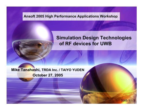
Ansoft 2005 High Performance Applications Workshop<br />
Mike Tanahashi, TRDA Inc. / TAIYO YUDEN<br />
October 27, 2005<br />
Simulation <strong>Design</strong> Technologies<br />
of RF devices for UWB<br />
2005/11/3
Corporate Overview<br />
• Headquarters: Tokyo, Japan<br />
• Establishment: March 1950<br />
• Capital: 23.5 Billion JPY<br />
• Consolidated Sales: ¥163.3 billion<br />
• Employees: 17,193 (worldwide)<br />
• WW Sales Offices: 37<br />
• WW Production Base: 20<br />
• WW R&D Bases: 6<br />
Sales Amount (bill Yen)<br />
200<br />
150<br />
100<br />
2<br />
50<br />
0<br />
Revenue<br />
Consolidated Sales<br />
1978 1980 1985 1990 1995<br />
2000<br />
2004<br />
2005<br />
Confidential<br />
Optical Media<br />
19%<br />
Sales by Products (FY03/04)<br />
Module<br />
12%<br />
Others<br />
9%<br />
Ferrite<br />
20%<br />
Capacitor<br />
40%<br />
Sales by Application (FY03/04)<br />
Components<br />
20%<br />
Others<br />
20%<br />
Automotive<br />
3%<br />
Computers<br />
21%<br />
Consumer<br />
20%<br />
Telecomms<br />
16%<br />
2005/11/3
3<br />
TAIYO YUDEN SALES BY PRODUCT MIX<br />
Advanced Thin<br />
Film Technology<br />
CD-R<br />
DVD-R<br />
Advanced Module Technology<br />
Bluetooth Module<br />
Ceramic <strong>Antenna</strong><br />
Diplexer<br />
Multilayer<br />
Piezo Speaker<br />
B.P.F.<br />
CCFL Inverter<br />
19%<br />
16%<br />
FY2004<br />
(W/W Sales)<br />
4%<br />
Multilayer<br />
Products<br />
46 %<br />
19%<br />
41%<br />
Multilayer<br />
Chip<br />
Inductors<br />
Advanced Ferrite Technology<br />
EMC<br />
Products<br />
SMD<br />
Power<br />
Inductor<br />
Advanced Multilayer Technology<br />
Advanced Capacitor Technology<br />
BME MLCCs Array<br />
Wound<br />
Chip<br />
Inductor<br />
Axial &<br />
Radial<br />
Inductor<br />
Axial Leaded<br />
2005/11/3
Contents<br />
4<br />
・What’s UWB?<br />
・<strong>Antenna</strong> for UWB<br />
・<strong>Filter</strong> & balun for UWB<br />
・Future development<br />
2005/11/3
Various RF st<strong>and</strong>ards <strong>and</strong> position UWB technologies<br />
5<br />
Expected new usage <strong>and</strong> field for UWB<br />
WBAN* WPAN WLAN WMAN・WWAN WRAN<br />
1Gbps<br />
100Mbps<br />
10Mbps<br />
1Mbps<br />
100kbps<br />
RFID、<br />
NFC<br />
1m<br />
UWB<br />
High-Data-<br />
Rate WPAN<br />
802.15.3a<br />
NG BT<br />
NG Bluetooth<br />
Bluetooth<br />
ZigBee, 802.15.4a<br />
10m<br />
802.11n<br />
802.11a/g<br />
802.11b<br />
100m<br />
802.16<br />
WiMAX<br />
NG Cellular<br />
Phone<br />
Cellular<br />
Phone<br />
802.20<br />
1Km<br />
* “WBAN” (Wireless Body Area Network) has not been officially used by st<strong>and</strong>ardization organizations.<br />
802.22<br />
WiTV<br />
100km<br />
2005/11/3
What’s UWB?<br />
6<br />
Frequency b<strong>and</strong>width of UWB <strong>and</strong> other RF st<strong>and</strong>ards<br />
Transmission output level (image)<br />
cell phone<br />
cell phone<br />
802.11b<br />
802.11g<br />
Bluetooth<br />
Spread spectrum communication<br />
such as existing narrow-b<strong>and</strong><br />
communication or wireless LAN<br />
GPS<br />
802.11a<br />
1 2 3 4 5 6 7 8 9 10 11<br />
frequency(GHz)<br />
Ultra Wideb<strong>and</strong><br />
(UWB communication)<br />
EMI regulation value<br />
under US FCC<br />
(FCC Part15)<br />
(-41.3dBm/MHz)<br />
2005/11/3
What’s UWB?<br />
7<br />
FCC approved UWB EIRP Level<br />
H<strong>and</strong>held Indoor<br />
2005/11/3
What’s UWB?<br />
8<br />
Features of UWB<br />
・ high-speed transmission (110Mbps-480Mbps)<br />
- Deliver multiple HDTV video stream<br />
- Transmission of low compression, no<br />
compressible AV<br />
- Cable replacement of USB2.0<br />
・ lower power consumption (
UWB application<br />
9<br />
Home application<br />
Short range<br />
Connectivity<br />
high throughput<br />
wired & wireless<br />
Home Office<br />
Cluster<br />
Family PC<br />
Cluster<br />
Broadb<strong>and</strong><br />
Data/Voice<br />
Access<br />
Long Range<br />
Networking/Connectivity<br />
wired & wireless<br />
Phone<br />
Broadb<strong>and</strong><br />
Video/Data<br />
Access<br />
Audio<br />
Cluster<br />
Home Theater<br />
Cluster<br />
Gaming<br />
Cluster<br />
Control<br />
Adapted from MBOA strategy press<br />
briefing h<strong>and</strong>out<br />
2005/11/3
UWB application<br />
10<br />
Office application<br />
Office Desktop<br />
Connectivity<br />
Wired /<br />
Wireless<br />
Conference Room<br />
Connectivity (Ad<br />
Hoc)<br />
Wired / Wireless<br />
LAN Connectivity<br />
Wired/Wireless<br />
IEEE 802.11a/g & n<br />
IEEE 802.3 Ethernet<br />
Broadb<strong>and</strong><br />
Access<br />
Intra-Campus<br />
Connectivity (Ad Hoc)<br />
Wired/Wireless<br />
Adapted from MBOA strategy press<br />
briefing h<strong>and</strong>out<br />
2005/11/3
Taiyo Yuden’s UWB Devices<br />
11<br />
UWB circuit needs the following passive components.<br />
<strong>Antenna</strong><br />
BPF BEF<br />
Balun<br />
RF<br />
Chip<br />
Base<br />
<strong>B<strong>and</strong></strong><br />
+<br />
MAC<br />
RF devices particular to UWB technology.<br />
・ UWB <strong>Antenna</strong><br />
・ <strong>B<strong>and</strong></strong> Pass <strong>Filter</strong> (BPF)<br />
・ <strong>B<strong>and</strong></strong> Elimination <strong>Filter</strong> (BEF)<br />
・ UWB Balun<br />
IEEE1394<br />
USB2.0<br />
PCI<br />
. . . . .<br />
2005/11/3
12<br />
• What’s UWB?<br />
• <strong>Antenna</strong> for UWB<br />
• <strong>Filter</strong> & balun for UWB<br />
• Future development trend<br />
2005/11/3
13<br />
The basic of antenna input impedance <strong>and</strong> radiation resistance<br />
Input impedance Zi→If you see antenna as a circuit,<br />
it is circuit constant characteristics of antenna<br />
when you see antenna part from I/O port<br />
Zi=Rr+Rl+jX<br />
Radiation resistance Resistance loss reactance<br />
e.g. half-wave dipole antenna<br />
73.13Ω<br />
As it gets bigger, heat loss will be increasing,<br />
<strong>and</strong> radiation efficiency of an antenna will be<br />
decreasing.<br />
Radiation efficiency =<br />
Rr<br />
Rr+Rl<br />
As Rr gets small, Rl cannot be ignored<br />
2005/11/3
14<br />
The basic of antenna Gain, efficiency <strong>and</strong> directivity<br />
Spherical radiation<br />
Balloon becomes<br />
spherical<br />
0dBi<br />
Blow air 1 into antenna<br />
The spherical shape is radiation pattern<br />
What’s that<br />
making gain<br />
higher?<br />
If try to break balloon?<br />
The volume of blown air is constant<br />
Integration value of directional pattern =1<br />
<strong>Antenna</strong> efficiency 100%<br />
Unit of gain → dBi (i→isotropic)<br />
-α(dB)<br />
It means that isotropic antenna is st<strong>and</strong>ard antenna for gain<br />
measurement.<br />
This is the ideal antenna that radiates equally in all directions.<br />
1<br />
dBd<br />
dBic<br />
dBil<br />
+α(dB)<br />
2005/11/3
Variety <strong>and</strong> principle of basic antenna<br />
Distribution<br />
of voltage<br />
Distribution<br />
of electric<br />
current<br />
15<br />
r<br />
λ/4<br />
(97mm@3.1GHz)<br />
monopole antenna<br />
If it’s bigger than 1λ, it gets close to infinity characteristics.<br />
It is finite actually.<br />
Ground plane<br />
(infinite size)<br />
It becomes antenna when ground plane<br />
exists.<br />
Ground plane is also one of the important part of antenna.<br />
λ/4<br />
If it’s smaller than 1λ,<br />
especially less than λ/4,<br />
characteristics changes drastically.<br />
advantage→It has simple structure that just<br />
set up the λ/4 element on the<br />
ground.<br />
disadvantage→The efficiency depends on configuration<br />
of ground. It is not for low profile<br />
because it needs to set up element for<br />
defrag I/O impedance.<br />
2005/11/3
16<br />
Variety <strong>and</strong> principle of basic antenna<br />
inverted-F antenna<br />
Short element<br />
(thick part)<br />
aboutλ/4<br />
Low-profile monopole antenna<br />
As same as monopole antenna, it becomes antenna when<br />
ground plane existence. But because of low-profile<br />
element, the coupling with ground that is right under<br />
element becomes strong. Therefore the efficiency does<br />
not depend on configuration of ground or size.<br />
Short element correct lowering of<br />
I/O impedance.<br />
advantage→it is easy to control I/O<br />
impedance.<br />
disadvantage→frequency b<strong>and</strong>width<br />
Ground plane<br />
becomes narrower.<br />
2005/11/3
Variety <strong>and</strong> principle of basic antenna dipole antenna<br />
17<br />
λ/4 λ/4<br />
Ground part of monopole antenna<br />
changes to linear λ/4 in length<br />
Unlike monopole antenna, characteristics is<br />
stable because of independent structure.<br />
It is used as a st<strong>and</strong>ard reference antenna<br />
due to its certain characteristics.<br />
advantage→stable characteristics.<br />
can be use for st<strong>and</strong>ard antenna.<br />
disadvantage→total length becomesλ/2,<br />
so it gets big.<br />
difficult to miniaturize.<br />
2005/11/3
18<br />
Variety <strong>and</strong> principle of ultra wide b<strong>and</strong> antenna<br />
<strong>Antenna</strong> electric volume<br />
(b<strong>and</strong>width)×(gain)×(efficiency)<br />
=constant value<br />
widen b<strong>and</strong>width without changing gain <strong>and</strong> efficiency<br />
Trade-off<br />
must make antenna electric volume bigger<br />
2005/11/3
Variety <strong>and</strong> principle of ultra wide b<strong>and</strong> antenna<br />
self-complementary antenna<br />
19<br />
Z<br />
Z‘<br />
ZZ‘=<br />
Z0<br />
4<br />
2<br />
≒(60π) 2<br />
Figure out antenna impedance<br />
of antenna that complement each<br />
other by Babinet’s principle.<br />
(Booker’s relation)<br />
In addition, board <strong>and</strong> hole are<br />
the exactly same.<br />
Z=<br />
2<br />
Z0 =60π<br />
(Mushiake’s relation)<br />
It is constant regardless of frequency<br />
<strong>and</strong> configuration<br />
Self-complementary antenna<br />
2005/11/3
Variety <strong>and</strong> principle of ultra wide b<strong>and</strong> antenna<br />
log-periodic antenna<br />
20<br />
β<br />
α<br />
Although structure is self-complementary,<br />
it has wide b<strong>and</strong>width characteristics for<br />
infinite spread. Therefore in principle<br />
b<strong>and</strong>width characteristics is smaller than<br />
self-complementary antenna.<br />
It is practical structure than<br />
self-complementary antenna<br />
Its structure is that antenna characteristics<br />
repeat periodically in proportion to log of frequency.<br />
Invented by DuHamel in 1955<br />
α+β=90°→self-complementary condition<br />
Rn+1<br />
Rn =τ(constant)→ log-periodic condition<br />
Element that is L distance from feed point<br />
decide resonance frequency.<br />
Maximum dimension decide<br />
adjustment resonance frequency.<br />
Input impedance=189Ω<br />
When α=45°τ=0.5, b<strong>and</strong>width is 5:1<br />
2005/11/3
Variety <strong>and</strong> principle of ultra wide b<strong>and</strong> antenna<br />
log-periodic dipole array antenna<br />
21<br />
L1<br />
α<br />
Feed line<br />
(feed with phase inversion)<br />
L2<br />
Approximately L1 decide minimum limit<br />
of resonance frequency. And L2 decide<br />
Guided wave area<br />
maximum limit of resonance frequency.<br />
Radiation area Example of design:α=10°、L1=63.5mm<br />
element number=15、L2=31.8mm<br />
Reflection area<br />
Each working area moves over<br />
by changing of frequency.<br />
b<strong>and</strong>width→1.1GHz~1.9GHz(less than VSWR2)<br />
gain →+8~+11dBi(Peak)<br />
2005/11/3
Variety <strong>and</strong> principle of ultra wide b<strong>and</strong> antenna discone antenna<br />
A<br />
22<br />
B<br />
Φ<br />
D<br />
disc<br />
conical<br />
feed line<br />
As thicken conductor diameter of dipole antenna,<br />
input impedance of antenna is improved.<br />
Widen b<strong>and</strong>width<br />
One part of dipole antenna is disc<br />
<strong>and</strong> the other parts are conical in shape.<br />
It feeds with coaxial cable.<br />
Example of design<br />
Minimum usage frequency fc=200MHz<br />
when D=230mm<br />
A=310mm<br />
B=350mm<br />
VSWR is less than 1.5 at 200~1000MHz<br />
2005/11/3
Variety <strong>and</strong> principle of ultra wide b<strong>and</strong> antenna<br />
spiral antenna (circular polarization antenna)<br />
23<br />
Archimedean spiral antenna Conical spiral antenna Quad line conical spiral antenna<br />
Electric wave radiate vertical<br />
direction to spiral plane.<br />
Input impedance 150~170Ω<br />
Stable frequency<br />
Axial direction<br />
excitation<br />
Side<br />
directional<br />
excitation<br />
can change direction to axial or side<br />
by the way of excitation of 4 lines.<br />
advantage: stable characteristics for wide b<strong>and</strong>width as circular polarization antenna<br />
disadvantage: need feeder circuit (ultra wide b<strong>and</strong> balun) for antenna structure<br />
2005/11/3
Variety <strong>and</strong> principle of ultra wide b<strong>and</strong> antenna<br />
double ridge horn antenna (directional antenna)<br />
24<br />
200<br />
150<br />
245<br />
Wide b<strong>and</strong>width by double ridge structure<br />
1~18GHz → less than VSWR3<br />
gain → +4.5dBi(@1GHz)<br />
~+14dBi(@16GHz)<br />
Used for transmitting antenna of antenna measurement<br />
2005/11/3
Evaluation of antenna characteristics<br />
25<br />
<strong>Antenna</strong><br />
under test<br />
VSWR<br />
(Voltage St<strong>and</strong>ing Wave Ratio)<br />
Network analyzer<br />
Important reminder for test<br />
・when you test antenna, it radiates electric wave. So set antenna up away<br />
from metal or human body etc. for unaffected.<br />
2005/11/3
Evaluation of antenna characteristics<br />
26<br />
Absolute gain<br />
2.15dBi<br />
St<strong>and</strong>ard dipole<br />
antenna<br />
<strong>Antenna</strong> under test<br />
<strong>Antenna</strong> under test<br />
Anechoic<br />
chamber<br />
Quiet Zone<br />
Turn table<br />
Transmitting horn antenna<br />
NETWORK ANALIZER<br />
gain <strong>and</strong><br />
radiation pattern<br />
Electric wave<br />
absorber were<br />
put on all six<br />
sides<br />
2005/11/3
Evaluation of antenna characteristics<br />
gain <strong>and</strong> radiation pattern<br />
27<br />
St<strong>and</strong>ard antenna<br />
e.g. St<strong>and</strong>ard dipole antenna<br />
Prs(dBm)<br />
Gs(dBi)<br />
Pt(dBm)<br />
Anechoic chamber<br />
Transmitting antenna<br />
e.g. Double ridge horn antenna Measured antenna Transmitting antenna<br />
e.g. Double ridge horn antenna<br />
Prt(dBm)<br />
Gain Gt=Prt-Prs+Gs<br />
rotate measurementΦ=270°<br />
antenna <strong>and</strong> plot Gt<br />
Radiation pattern<br />
Gt(dBi)<br />
rotation φ<br />
Φ=0°<br />
Φ=180°<br />
Gain(dBi)<br />
Pt(dBm)<br />
Φ=90°<br />
2005/11/3
28<br />
Evaluation of antenna characteristics efficiency<br />
3D radiation pattern by antenna near field measurement system<br />
31 sensors<br />
rotation<br />
antenna under test<br />
Measuring antenna efficiency<br />
Integration value of 3D<br />
Radiation pattern<br />
is the antenna efficiency.<br />
2005/11/3
Evaluation of antenna characteristics group delay<br />
Anechoic<br />
chamber<br />
29<br />
RF-Amp<br />
UWB<br />
antenna<br />
measure delay of<br />
S21 characteristics<br />
double ridge horn antenna<br />
Example of measurement<br />
2005/11/3
Comparison of simulation values of UWB antenna<br />
analysis model<br />
30<br />
Z<br />
Y<br />
ground<br />
<strong>Antenna</strong> element<br />
X<br />
Producing condition close to<br />
measurement environment<br />
Full-featured CAD, takes about 30<br />
minutes to make model<br />
For improvement of accuracy of analysis<br />
GND affects antenna characteristics <strong>and</strong> we<br />
generate fine mesh manually on GND in<br />
advance.<br />
2005/11/3
31<br />
Comparison of simulation values of UWB antenna<br />
VSWR<br />
cable<br />
Cable used for measurement<br />
may affect.<br />
Actual measurement result<br />
Simulation<br />
result<br />
Almost congruent under<br />
no practical issue.<br />
2005/11/3
Comparison of simulation values of UWB antenna<br />
32<br />
antenna efficiency<br />
Actual measurement<br />
result<br />
<strong>Antenna</strong> efficiency was measured by STARGATE in Taiyo Yuden.<br />
Almost congruent under<br />
no practical issue.<br />
Simulation result<br />
antenna efficiencyantenna efficiency<br />
For the feature of antenna that used for measurement,<br />
the difference between measurement <strong>and</strong> simulation<br />
may be error.<br />
31 sensors<br />
rotation<br />
AUT<br />
2005/11/3
33<br />
Comparison of simulation values of UWB antenna<br />
radiation pattern(3.1GHz)<br />
2005/11/3
34<br />
Comparison of simulation values of UWB antenna<br />
radiation pattern(4.0GHz)<br />
2005/11/3
Comparison of simulation values of UWB antenna<br />
35<br />
radiation pattern(5.0GHz)<br />
2005/11/3
36<br />
Comparison of simulation values of UWB antenna<br />
radiation pattern(6.5GHz)<br />
2005/11/3
Comparison of simulation values of UWB antenna<br />
37<br />
radiation pattern(7.5GHz)<br />
2005/11/3
38<br />
Application of simulation of UWB antenna<br />
field intensity<br />
3.1GHz<br />
4GHz 5GHz<br />
6.5GHz 7.5GHz<br />
2005/11/3
<strong>Antenna</strong> characteristics used for UWB system<br />
39<br />
frequency b<strong>and</strong>width<br />
gain <strong>and</strong> directivity<br />
Base station<br />
Intended specific<br />
direction<br />
Directional antenna<br />
(≒10dBi)<br />
3.1GHz ~ 10.6GHz<br />
will change by application used in<br />
specific communication systems<br />
Intended wide<br />
direction<br />
Within horizontal plane<br />
Omni directional antenna<br />
(≒3dBi)<br />
Mobile station(mobile terminal etc.)<br />
Unsettled condition (direction)<br />
of equipment<br />
Spherical directional pattern<br />
(≒0dBi)<br />
2005/11/3
UWB <strong>Antenna</strong><br />
40<br />
Shapes & dimensions<br />
VSWR<br />
8 x 6 x 1mm<br />
VSWR<br />
7<br />
6<br />
5<br />
4<br />
3<br />
2<br />
1<br />
2 3 4 5 6 7 8 9 10 11 12<br />
Frequency (GHz)<br />
Features<br />
� lower VSWR<br />
� flat gain<br />
� flat group delay<br />
� compact<br />
� lower cost<br />
� omni directional<br />
� 50Ωimpedance<br />
UWB antenna needs to transmit <strong>and</strong><br />
receive signal for wide b<strong>and</strong>width.<br />
2005/11/3
Contents<br />
41<br />
• What’s UWB?<br />
• <strong>Antenna</strong> for UWB<br />
• <strong>Filter</strong> & balun for UWB<br />
• Future development<br />
2005/11/3
<strong>Design</strong> for Strip line type <strong>Filter</strong><br />
42<br />
Basic design<br />
Wave shortening design<br />
≒<br />
L<br />
L C L C<br />
C<br />
=<br />
4 f<br />
0<br />
ε<br />
r<br />
・the length of strip line decide frequency<br />
・dielectric constant material can make resonator shorter<br />
Cs<br />
f<br />
1<br />
=<br />
2π<br />
LC<br />
1<br />
f '=<br />
2π<br />
L(C+<br />
Cs)<br />
・possible to miniaturize by parallel<br />
capacitance with strip line<br />
2005/11/3
<strong>Design</strong> for Strip line type <strong>Filter</strong><br />
43<br />
Trap design<br />
3rd<br />
1st trap<br />
trap<br />
2nd<br />
trap<br />
1st resonator 2nd resonator 3rd resonator<br />
・possible to make trap by circuit structure<br />
[dB]<br />
0<br />
-10<br />
-20<br />
-30<br />
-40<br />
-50<br />
-60<br />
-70<br />
-80<br />
-90<br />
-100<br />
2000 7000<br />
freq.[MHz]<br />
12000<br />
2005/11/3
<strong>Design</strong> for Strip line type Balun<br />
44<br />
L<br />
Unbalance Port<br />
C<br />
=<br />
4 f<br />
0<br />
ε<br />
r<br />
Balance Port<br />
λ/4 Resonator<br />
Main electric characteristics<br />
-Balance Impedance<br />
-Insertion loss at pass b<strong>and</strong><br />
-Phase balance<br />
-Amplitude balance<br />
・the length of strip line decide frequency<br />
・dielectric constant material can make resonator shorter<br />
・coupling of λ/4 resonator decide b<strong>and</strong>width<br />
2005/11/3
Required performance of RF device for UWB<br />
10dB<br />
45<br />
BW(-10dB b<strong>and</strong> width) ≧ 1/5 fc<br />
or more than 500MHz b<strong>and</strong> width<br />
Transmitting output<br />
BW<br />
fc<br />
frequency<br />
need to satisfy electric<br />
characteristics of filter <strong>and</strong><br />
balun with wide b<strong>and</strong>width<br />
<br />
<strong>Filter</strong><br />
Balun<br />
-Insertion loss at pass b<strong>and</strong><br />
-Insertion loss at pass b<strong>and</strong><br />
-Phase imbalance<br />
-Amplitude imbalance<br />
2005/11/3
Importance of simulation technologies<br />
46<br />
traditional :Cut & Try<br />
Circuit Simulation CAD<br />
present:Simulation<br />
HFSS Simulation<br />
Specification<br />
arrangement<br />
trial<br />
3-5 rotation<br />
trial evaluation MP<br />
evaluation<br />
MP<br />
Specification<br />
arrangement<br />
Short lead time<br />
Save cost<br />
2005/11/3
Evaluation Method<br />
47<br />
Measurement outline<br />
N.W.A<br />
DUT<br />
Method<br />
Cancel of jig loss<br />
De-embedded<br />
Merit<br />
Easy to get attenuation<br />
characteristics<br />
S-parameter data available<br />
After calibrate with cable terminal <strong>and</strong> measure<br />
S-Parameter of filter with board or SMA<br />
connector, cancel board or SMA connector then<br />
derive only filter characteristics.<br />
Demerit<br />
No S-parameter data<br />
2005/11/3
Comparison of simulation <strong>and</strong> actual measurement<br />
value<br />
48<br />
Comparison by through jig<br />
Transmission characteristics of<br />
S11 <strong>and</strong> S21is congruent.<br />
But・・・<br />
Develop into a gap in<br />
Smith’s chart!<br />
Cannot be used as S-Parameter!<br />
-<br />
-<br />
-<br />
-<br />
Actual<br />
measurement_S11<br />
Actual<br />
measurement_S21<br />
simulation_S33<br />
simulation_S43<br />
2005/11/3
Comparison of simulation <strong>and</strong> actual measurement<br />
value<br />
49<br />
De-embedding method<br />
Example of structure for De-embedding<br />
Port1 Port2<br />
Actual measurement data<br />
before De-embedding<br />
Port2<br />
Simulation result of above<br />
Port1<br />
Simulation result of DUT only<br />
comparison<br />
Re-create SMA by HFSS<br />
2005/11/3
Comparison of simulation <strong>and</strong> actual measurement<br />
value<br />
50<br />
Comparison by De-embedding<br />
Simulation value <strong>and</strong> actual<br />
measurement value is congruent<br />
including Smith’s chart.<br />
-<br />
-<br />
-<br />
-<br />
Actual<br />
measurement_S11<br />
Actual<br />
measurement_S21<br />
simulation_S33<br />
simulation_S43<br />
2005/11/3
Comparison of simulation <strong>and</strong> actual measurement<br />
value<br />
51<br />
Comparison by Balun(De-embedding)<br />
As same as BPF, simulation <strong>and</strong> actual<br />
measurement is congruent by De-embedding.<br />
Pass/Attenuation Amplitude imbalance Phase imbalance<br />
2005/11/3
UWB-<strong>B<strong>and</strong></strong> Pass <strong>Filter</strong> (BPF)<br />
52<br />
Shapes & dimensions<br />
2.0 x 1.25 x 1.0mm(Max)<br />
Electric characteristicss<br />
S11/S21(dB)<br />
0<br />
-10<br />
-20<br />
-30<br />
-40<br />
-50<br />
S11<br />
S21<br />
1000 2000 3000 4000 5000 6000<br />
Freq(MHz)<br />
Features<br />
� Lower insertion loss <strong>and</strong> higher attenuation<br />
� Suitable for the first generation UWB chip set<br />
(3-5GHz)<br />
� Smaller size<br />
� Lower cost<br />
� 50Ω- input/output<br />
BPF prevents UWB from interfering with mobile phones,<br />
GPS, 2.4GHz or 5GHz-Wireless LAN System <strong>and</strong> also<br />
prevents these applications from interfering with UWB.<br />
2005/11/3
UWB-<strong>B<strong>and</strong></strong> Elimination <strong>Filter</strong> (BEF)<br />
53<br />
Shapes & dimensions<br />
6.3 x 3.0 x 1.1mm(Max)<br />
Electric characteristicss<br />
Features<br />
� Lower insertion loss <strong>and</strong> higher attenuation at 5GHz<br />
� Smaller size<br />
�50Ω- input/output<br />
BEF is essential, for the b<strong>and</strong>widths of<br />
5GHz Wireless LAN <strong>and</strong> UWB are close.<br />
It is not enough in attenuation to use only<br />
BPF.<br />
2005/11/3
UWB-Balun<br />
54<br />
Shapes & dimensions<br />
3.2 x 2.5 x 1.0mm(Max)<br />
Electric characteristicss<br />
Loss (dB)<br />
0<br />
-5<br />
-10<br />
-15<br />
-20<br />
-25<br />
-30<br />
-35<br />
-40<br />
Transmission<br />
Features<br />
1 2 3 4 5 6 7 8 9<br />
Frequency (GHz)<br />
� Lower phase error <strong>and</strong> lower amplitude error<br />
� Lower insertion loss<br />
� Suitable for the first <strong>and</strong> second generation UWB<br />
chipsets<br />
� 50:100Ω-impedance<br />
Return Loss<br />
Insertion Loss<br />
Balun is essential for unbalance (unbalance, single-end) -<br />
balance (balance, differential) signal conversion.<br />
Amplitude (dB)<br />
3<br />
2<br />
1<br />
0<br />
-1<br />
-2<br />
-3<br />
Imbalance<br />
Amplitude<br />
Phase<br />
1 2 3 4 5 6 7 8 9<br />
Frequency (GHz)<br />
15<br />
10<br />
5<br />
0<br />
-5<br />
-10<br />
-15<br />
Phase (deg)<br />
2005/11/3
UWB-Balun<br />
55<br />
Shapes & dimensions<br />
2.0 x 1.25x 0.9mm<br />
Electric characteristicss<br />
Loss<br />
0<br />
-5<br />
-10<br />
-15<br />
-20<br />
-25<br />
-30<br />
Freqency Response<br />
Features<br />
� Lower phase error <strong>and</strong> lower amplitude error<br />
� Lower insertion loss<br />
�Smaller size & Lower cost<br />
� 50:100Ω-impedance<br />
Return Loss<br />
Insertion Loss<br />
3.0 3.5 4.0 4.5 5.0<br />
Frequency<br />
Balun is essential for unbalance (unbalance, single-end) -<br />
balance (balance, differential) signal conversion.<br />
AmplitudeImbalance(dB)<br />
2.5<br />
2.0<br />
1.5<br />
1.0<br />
0.5<br />
0.0<br />
-0.5<br />
-1.0<br />
-1.5<br />
-2.0<br />
-2.5<br />
Freqency Response<br />
Amplitude Imbalance<br />
Phase Imbalance<br />
3.0 3.5 4.0 4.5 5.0<br />
Frequency (GHz)<br />
10<br />
8<br />
6<br />
4<br />
2<br />
0<br />
-2<br />
-4<br />
-6<br />
-8<br />
-10<br />
Phase Imbalance (deg)<br />
2005/11/3
Contents<br />
56<br />
• What’s UWB?<br />
• <strong>Antenna</strong> for UWB<br />
• <strong>Filter</strong> & balun for UWB<br />
• Future development<br />
2005/11/3
<strong>Antenna</strong> line up<br />
57<br />
Wide <strong>B<strong>and</strong></strong> <strong>Antenna</strong><br />
Inverted F <strong>Antenna</strong><br />
Dual <strong>B<strong>and</strong></strong> <strong>Antenna</strong><br />
Helical <strong>Antenna</strong><br />
2.4GHz<br />
5GHz<br />
500MHz 1GHz 2GHz 5GHz<br />
Bluetooth<br />
W-LAN 11b/g<br />
3~10GHz<br />
W-LAN 11a<br />
W-LAN 11a/b/g<br />
GPS<br />
UWB<br />
Inverted F<br />
Monopole<br />
Inverted F<br />
Monopole<br />
Dual b<strong>and</strong><br />
8x3x1mm 10x4x1mm 12x2x1mm<br />
2.5x1.6x1.6mm<br />
4x2x0.8mm<br />
11x1.6x1.6mm<br />
Proto<br />
10x4x1mm<br />
NEW<br />
2005/11/3
<strong>Filter</strong> & Balun line up<br />
58<br />
SL type <strong>Filter</strong><br />
Balun<br />
Balance <strong>Filter</strong><br />
LC type <strong>Filter</strong><br />
2.4GHz<br />
5GHz<br />
500MHz 1GHz 2GHz 5GHz<br />
Bluetooth<br />
W-LAN 11b/g<br />
1.7~5GHz<br />
W-LAN 11a<br />
Digital TV<br />
UWB<br />
BPF<br />
Balance<br />
BPF<br />
BPF<br />
LPF<br />
Balance<br />
BPF<br />
BPF<br />
2.5x2.0x1.0max<br />
2.0x1.25x1.0max<br />
2.0x1.25x1.0max<br />
2.0x1.25x1.0max<br />
2.0x1.25x1.0max<br />
Under Development<br />
2.0x1.25x1.0max<br />
MP 2005.8~<br />
MP 2005.10~<br />
Under Development<br />
Balun<br />
Under Development<br />
2005/11/3
Total solution for TAIYO YUDEN’s UWB<br />
59<br />
Providing Total UWB Ecosystem<br />
RF Passive Components<br />
Total solution<br />
<strong>Antenna</strong> & support Certification Services Module<br />
IC/Firmware/Software<br />
UWB Products<br />
USB Dongle<br />
ExpressCard<br />
Collaboration<br />
Quick introduction to<br />
the market<br />
2005/11/3
Contact information<br />
60<br />
For US/EU <strong>and</strong> other regions :<br />
Mike Tanahashi<br />
TRDA Inc.<br />
Taiyo Yuden R&D Center of America<br />
email: mtanahashi@trda-inc.com<br />
For Asia : NOBUAKI SAITO<br />
Products Planning Division<br />
Marketing Headquarters<br />
JAPAN Taiyo Yuden<br />
email: nsaito@jty.yuden.co.jp<br />
Hiroshi Homma<br />
Overseas Sales Division<br />
JAPAN Taiyo Yuden<br />
email: h-homma@jty.yuden.co.jp<br />
2005/11/3
61<br />
Thank you for your attention.<br />
2005/11/3


