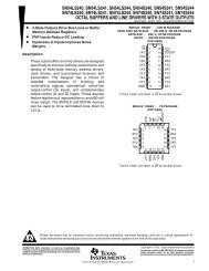
74245 Octal Bus Transceiver - CCSE
74245 Octal Bus Transceiver - CCSE
74245 Octal Bus Transceiver - CCSE

You also want an ePaper? Increase the reach of your titles
YUMPU automatically turns print PDFs into web optimized ePapers that Google loves.
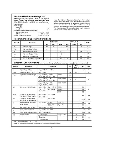
Absolute Maximum Ratings (Note)<br />
If MilitaryAerospace specified devices are required<br />
please contact the National Semiconductor Sales<br />
OfficeDistributors for availability and specifications<br />
Supply Voltage<br />
Input Voltage<br />
7V<br />
DIR or G 7V<br />
A or B<br />
Operating Free Air Temperature Range<br />
55V<br />
DM54LS and 54LS<br />
b55Ctoa125C<br />
DM74LS 0Ctoa70C<br />
Storage Temperature Range<br />
b65Ctoa150C<br />
Recommended Operating Conditions<br />
Symbol Parameter<br />
Note The ‘‘Absolute Maximum Ratings’’ are those values<br />
beyond which the safety of the device cannot be guaranteed<br />
The device should not be operated at these limits The<br />
parametric values defined in the ‘‘Electrical Characteristics’’<br />
table are not guaranteed at the absolute maximum ratings<br />
The ‘‘Recommended Operating Conditions’’ table will define<br />
the conditions for actual device operation<br />
DM54LS245 DM74LS245<br />
Min Nom Max Min Nom Max<br />
V CC Supply Voltage 45 5 55 475 5 525 V<br />
VIH High Level Input Voltage 2 2 V<br />
VIL Low Level Input Voltage 07 08 V<br />
I OH High Level Output Current b12 b15 mA<br />
IOL Low Level Output Current 12 24 mA<br />
TA Free Air Operating Temperature b55 125 0 70 C<br />
Electrical Characteristics over recommended operating free air temperature range (unless otherwise noted)<br />
Symbol Parameter Conditions Min<br />
Typ<br />
(Note 1)<br />
Units<br />
Max Units<br />
VI Input Clamp Voltage VCC e Min II eb18 mA b15 V<br />
HYS Hysteresis (VTa b VTb) VCC e Min 02 04 V<br />
VOH High Level Output Voltage VCC e Min VIH e Min<br />
VIL e Max IOH eb1mA<br />
DM74<br />
VCC e Min VIL e Min DM54DM74<br />
VIL e Max IOH eb3mA<br />
VCC e Min VIH e Min DM54DM74<br />
VIL e 05V IOH e Max<br />
27<br />
24 34 V<br />
VOL Low Level Output Voltage VCC e Min IOL e 12 mA DM74 04<br />
VIL e Max<br />
VIH e Min<br />
IOL e Max DM54<br />
DM74<br />
04<br />
05<br />
V<br />
IOZH Off-State Output Current VCC e Max VO e 27V<br />
High Level Voltage Applied VIL e Max<br />
IOZL Off-State Output Current<br />
Low Level Voltage Applied<br />
VIH e Min<br />
VO e 04V<br />
II Input Current at Maximum VCC e Max AorB VIe55V 01<br />
Input Voltage<br />
DIR or G VI e 7V 01<br />
2<br />
20 mA<br />
b200 mA<br />
IIH High Level Input Current VCC e Max VI e 27V 20 mA<br />
I IL Low Level Input Current V CC e Max V I e 04V b02 mA<br />
IOS Short Circuit Output Current VCC e Max (Note 2) b40 b225 mA<br />
ICC Supply Current Outputs High VCC e Max 48 70<br />
Note 1 All typicals are at VCC e 5V TA e 25C<br />
Note 2 Not more than one output should be shorted at a time not to exceed one second duration<br />
Outputs Low 62 90 mA<br />
Outputs at Hi-Z 64 95<br />
2<br />
mA