Oscillators
Oscillators
Oscillators

Create successful ePaper yourself
Turn your PDF publications into a flip-book with our unique Google optimized e-Paper software.
<strong>Oscillators</strong><br />
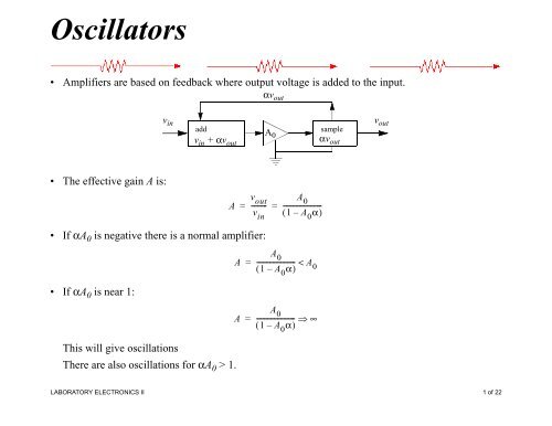
• Amplifiers are based on feedback where output voltage is added to the input.<br />
The effective gain A is:<br />
If αA 0 is negative there is a normal amplifier:<br />
If αA 0 is near 1:<br />
This will give oscillations<br />
There are also oscillations for αA0 > 1.<br />
LABORATORY ELECTRONICS II<br />
v in<br />
add<br />
v in + αv out<br />
A<br />
A<br />
A<br />
αv out<br />
A 0<br />
vout = --------- =<br />
vin =<br />
A0 -----------------------<br />
( 1 – A0α )<br />
A0 ----------------------- < A<br />
( 1 – A0α) 0<br />
A0 =<br />
----------------------- ⇒ ∞<br />
( 1 – A0α) sample<br />
αv out<br />
v out<br />
1 of 22
Signal Phase<br />
Positive feedback must be in phase to compensate for energy lost on each oscillation.<br />
The low pass filter provides a phase shift that depends on the frequency.<br />
v 0<br />
The phase can be expressed in terms of the complex impedance.<br />
The phase depends on the frequency:<br />
At high frequency, φ -> −90<br />
At ω = 1/RC, φ = −45<br />
At low frequency, φ -> 0<br />
LABORATORY ELECTRONICS II<br />
B<br />
R<br />
=<br />
B 2 C 2<br />
+<br />
C<br />
i<br />
v C<br />
1<br />
1 ω 2 R 2 C 2<br />
-----------------------------<br />
+<br />
φ<br />
jC<br />
φ<br />
A<br />
=<br />
1 ⁄ jωC<br />
= ------------------------------- =<br />
( 1 ⁄ jωC ) + R<br />
– jωRC<br />
1 ω 2 R 2 C 2<br />
-----------------------------<br />
+<br />
1 – jωRC<br />
1 ω 2 R 2 C 2<br />
-----------------------------<br />
+<br />
– ωRC<br />
= atan-------------- = atan(<br />
– ωRC)<br />
1<br />
2 of 22
Wien Bridge Oscillator<br />
The Wien bridge oscillator uses positive feedback to<br />
get a phase shift on an RC filter.<br />
The positive feedback can be calculated from the RC<br />
filters.<br />
The RC networks provide a voltage divider for the non-inverting input.<br />
The inverting input must be equal to the non-inverting input so the variable resistor voltage divider<br />
should be set to 1/3.<br />
Matching terms in the complex expression is called phase cancellation.<br />
The frequency ω is the point of stable oscillations.<br />
LABORATORY ELECTRONICS II<br />
ZRCser = 1 ⁄ ( jωC ) + R =<br />
Z RCpar<br />
R ⁄ jωC<br />
= ------------------------------- =<br />
1 ⁄ ( jωC ) + R<br />
v non<br />
1 + jωRC<br />
----------------------jωC<br />
-----------------------<br />
R<br />
1 + jωRC<br />
ZRCpar = ----------------------------------------- v<br />
ZRCpar + Z out =<br />
RCser<br />
50 kΩ<br />
0 = jωRC + 1 ⁄ ( jωRC)<br />
ω =<br />
1 ⁄ RC<br />
R C<br />
v inv<br />
v non<br />
-------------------------------------------------------<br />
1<br />
v<br />
jωRC + 1 ⁄ ( jωRC)<br />
+ 3 out<br />
−<br />
+<br />
C<br />
R<br />
v out<br />
3 of 22
Self-Regulating Feedback<br />
It is very difficult to get the oscillator feedback set to exactly 1/3.<br />
The Wien bridge oscillator could be better with a<br />
resistance on the inverting input that varies with<br />
current, eg. a lamp.<br />
Another solution is to use an FET as the variable<br />
resistor. The RC delay on the signal to the FET gate<br />
makes the circuit resistance vary slowly compared to<br />
the frequency of oscillation.<br />
LABORATORY ELECTRONICS II<br />
1 MΩ 2.2 μF<br />
1.0 μF<br />
R C<br />
vinv −<br />
vnon +<br />
10 kΩ<br />
C<br />
470 Ω<br />
R<br />
R C<br />
v out<br />
v inv<br />
v non<br />
−<br />
+<br />
C<br />
R<br />
v out<br />
4 of 22
LC <strong>Oscillators</strong><br />
The Colpitts oscillator uses an LC resonance to establish the oscillation.<br />
C 1<br />
The inverting input is a parallel LC circuit (impedance divider) and the positive feedback is<br />
through the capacitor.<br />
The Hartley oscillator also uses an LC resonance to establish the oscillation.<br />
L 1<br />
LABORATORY ELECTRONICS II<br />
C<br />
L<br />
−<br />
+<br />
−<br />
+<br />
C 2<br />
L 2<br />
v out<br />
v out<br />
ω =<br />
ω =<br />
-----------------------<br />
1<br />
LC1C2 -------------------<br />
C1 + C2 -------------------------------<br />
1<br />
( L1 + L2)C 5 of 22
Crystal <strong>Oscillators</strong><br />
A quartz crystal converts strain into voltage through piezoelectricity:<br />
The schematic symbol for a crystal:<br />
There are natural crystal oscillations equivalent to an RLC circuit.<br />
The crystal oscillator forms a tuned LC-feedback for the op-amp.<br />
The crystal is usually only marked with the characteristic frequency.<br />
LABORATORY ELECTRONICS II<br />
10 kΩ<br />
R L C s<br />
v out<br />
Cm » Cs 100 kΩ<br />
−<br />
+<br />
150 kHz<br />
v out<br />
6 of 22
Comparator<br />
A comparator returns one of two values based on whether the input is greater or less than a<br />
reference value.<br />
An op-amp can function directly as an analog comparator.<br />
The logic states are v out = V CC if v in > V ref ; v out = V EE if v in < V ref .<br />
Low-battery indicator<br />
V bb is the value to be tested, V CC supplies power to the tester.<br />
LABORATORY ELECTRONICS II<br />
V bb<br />
vin Vref R 3<br />
V Z<br />
+<br />
−<br />
V CC<br />
V EE<br />
R 2<br />
R 1<br />
V cc<br />
+<br />
−<br />
v out<br />
v out<br />
7 of 22
Schmitt Trigger<br />
The Schmitt trigger is a circuit with binary output that has thresholds at two different voltages<br />
depending on the present state of the output.<br />
This combines analog elements with binary logic.<br />
The non-inverting input of the op-amp has a threshold which solely based on the three resistors and<br />
V ref and v out.<br />
For equal resistors and 5 V supply, v th=1.67 V or 3.33 V for v out = 0 V or 5 V respectively.<br />
LABORATORY ELECTRONICS II<br />
v in<br />
R 2<br />
R 1<br />
V ref<br />
−<br />
+<br />
R 3<br />
v out<br />
vth = Vref – i2R2 = vout – i3R3 = i1R1 = ( i2 + i3)R1 v ⎛----- 1<br />
-----<br />
1 1<br />
th + + ----- ⎞<br />
⎝R1R2R⎠ 3<br />
=<br />
Vref vout --------- + ---------<br />
R2 R3 8 of 22
Hysteresis<br />
The Schmitt trigger circuit has one threshold when approaching from a low voltage state and a<br />
different one when approaching from a high voltage state.<br />
The effect of having different thresholds for different directions is called hysteresis.<br />
A plot of the input versus output shows the hysteresis diagram.<br />
LABORATORY ELECTRONICS II<br />
Input<br />
Output<br />
V out<br />
5 V<br />
3.3 V<br />
1.7 V<br />
5 V<br />
1.7 V 3.3 V 5 V Vin 9 of 22
Relaxation Oscillator<br />
The relaxation oscillator uses<br />
an RC network on the<br />
inverting input.<br />
A current flowing through Rf can charge or discharge the<br />
capacitor C with a time<br />
constant t = RfC. The threshold for the output<br />
shifts due to the hysteresis of<br />
the amplifier.<br />
The output voltage is set at either +VCC or -VCC depending on the relative values of Vcap and Vthr ,<br />
and the period depends on Vthr/Vout. LABORATORY ELECTRONICS II<br />
V cap<br />
C<br />
R 1<br />
R f<br />
V thr<br />
V CC Vcap<br />
– VCC<br />
V CC Vout<br />
– VCC<br />
−<br />
+<br />
R 2<br />
I<br />
t<br />
t<br />
V out<br />
V thr<br />
=<br />
R1 ------------------V<br />
R1 + R out<br />
2<br />
Vcap Vout ( Vthr + Vout)e t – R ⁄ fC<br />
= –<br />
Vout ---------- = V<br />
2 out<br />
1<br />
--<br />
2<br />
⎛ T<br />
– -- ⎞<br />
3 ⎝ 2⎠<br />
⁄ ( RC)<br />
= --e<br />
2<br />
⎛ T<br />
– -- ⎞<br />
3 ⎝ 2⎠<br />
⁄ ( RC)<br />
– --V<br />
2 oute T =<br />
2RCln3 ≅ 2.2RC<br />
10 of 22
Triangle-Wave Oscillator<br />
The relaxation oscillator can be modified to charge the capacitor with a constant current.<br />
V cap<br />
C<br />
The JFET pair is Q1 and Q2. When the gate is more positive the JFET conducts, if the gate is more<br />
negative it acts as a current source.<br />
When Vout = −VCC : Q1 conducts and Q2 provides constant current.<br />
When V out = +V CC : Q 2 conducts and Q 1 provides constant current.<br />
LABORATORY ELECTRONICS II<br />
R 1<br />
R<br />
V thr<br />
−<br />
+<br />
R 2<br />
Q 1<br />
Q 2<br />
R<br />
I<br />
V thr<br />
V cap<br />
V out<br />
=<br />
R1 ------------------V<br />
R1 + R out<br />
2<br />
=<br />
1<br />
= --- Idt C∫<br />
=<br />
It<br />
---<br />
C<br />
λV out<br />
11 of 22
Triangle Timing<br />
The signal at V cap is a ramp from −λV CC to +λV CC .<br />
The period is<br />
LABORATORY ELECTRONICS II<br />
V CC<br />
– VCC<br />
V CC V out<br />
– VCC<br />
The triangle wave is not from V out but instead from V cap.<br />
T<br />
=<br />
4λCVCC ---------------------<br />
I<br />
V cap<br />
t<br />
t<br />
12 of 22
Monostable Multivibrator<br />
The monostable multivibrator, also called a one-shot, is a device with two output states that has<br />
one stable state and another of fixed duration.<br />
An op-amp one-shot can be made from a relaxation oscillator.<br />
Here the negative feedback capacitor is shorted by a diode, V C
One-Shot Recovery Time<br />
Dead time is the time when a device cannot function normally.<br />
The recovery time as the capacitor is charging towards 0.6 V a new trigger would need to be<br />
sufficiently negative to permit refiring.<br />
With the resistor divider, this is not generally possible and no trigger is accepted during this period.<br />
15 V<br />
LABORATORY ELECTRONICS II<br />
0.6 V<br />
15 V<br />
V in<br />
V out<br />
14 of 22
Inverter One-Shot<br />
A digital inverter can be used as a one-shot.<br />
The input pulse is altered by the high-pass filter.<br />
The falling edge of the input pulse has no effect,<br />
but the rising edge produces a pulse into the<br />
inverter that crosses the threshold for a time<br />
proportional to RC.<br />
5 V<br />
2.5 V<br />
5 V<br />
LABORATORY ELECTRONICS II<br />
V in<br />
V out<br />
1<br />
--V<br />
2 0<br />
=<br />
t RC<br />
V0e ⁄ –<br />
V in<br />
t = RClog2 =<br />
0.693RC<br />
C<br />
R<br />
V out<br />
15 of 22
Astable Multivibrator<br />
An astable multivibrator is a square wave generator.<br />
The output of a monostable multivibrator can feed back to retrigger another one-shot cycle.<br />
When V out = +5, V C is charged towards ground from V 2.<br />
As the input V 1 drops below the logic threshold, V 2 = +5 and V out = 0.<br />
When V out = 0, V C is charged towards +5 from V 2.<br />
The system oscillates between the two states.<br />
LABORATORY ELECTRONICS II<br />
V 1<br />
R 2<br />
V 2<br />
R 1 C<br />
V C<br />
R1 ≅ 10R2 f<br />
1<br />
≈<br />
----------<br />
R2C V out<br />
16 of 22
Integrated Circuit One-Shots<br />
Making a one-shot from gates leaves a design that depends on the individual component<br />
characteristics.<br />
Integrated one-shots avoid component variations, and require only the external resistor and<br />
capacitor to set RC.<br />
A, B and X can trigger the one-shot, A with a falling edge, B and X with rising edges. X also acts<br />
as a reset for Q.<br />
R and C set the time constant for the output pulse. As long as an input triggers the circuit the<br />
output will continue to retrigger.<br />
LABORATORY ELECTRONICS II<br />
+V CC<br />
R<br />
74LS123 C<br />
A<br />
B<br />
X<br />
Q<br />
Q<br />
17 of 22
555 Timer<br />
One of the most important<br />
multivibrators is the 555 timer.<br />
The 555 uses two internal thresholds.<br />
There are three external points, one is<br />
set by the external RC network, one<br />
by an external pulse, and one is used<br />
to discharge the capacitor.<br />
In this configuration the 555 timer<br />
acts as a one-shot.<br />
The input pulse starts the charging<br />
capacitor.<br />
When the threshold is reached the<br />
capacitor discharges.<br />
V CC<br />
TRG<br />
THR<br />
OUT<br />
The output pulse length is T = RCln3 = 1.1RC.<br />
LABORATORY ELECTRONICS II<br />
2/3 VCC 1/3 VCC R<br />
BAL<br />
THR<br />
TRG<br />
DIS<br />
C<br />
5 kΩ<br />
−<br />
+<br />
5 kΩ<br />
−<br />
+<br />
5 kΩ<br />
GND<br />
RST<br />
+V CC<br />
555<br />
S<br />
R<br />
Q<br />
Q<br />
OUT<br />
18 of 22
555 as an Astable Multivibrator<br />
The 555 can be wired as an oscillator.<br />
The capacitor is charged is through R 1<br />
and R 2.<br />
The capacitor is discharged only<br />
through R 2 .<br />
The two states will have unequal<br />
duration.<br />
THR<br />
OUT<br />
The output pulse length is<br />
T = (R1 + R2 )Cln2 + R2Cln2 = 0.693(R1 + 2R2 )C.<br />
LABORATORY ELECTRONICS II<br />
2/3 VCC 1/3 VCC R 2<br />
C<br />
R 1<br />
BAL<br />
THR<br />
TRG<br />
DIS<br />
5 kΩ<br />
−<br />
+<br />
5 kΩ<br />
−<br />
+<br />
5 kΩ<br />
GND<br />
RST<br />
+V CC<br />
555<br />
S<br />
R<br />
Q<br />
Q<br />
OUT<br />
19 of 22
Duty Cycle<br />
The ratio of the high part of the cycle to the period is the duty cycle.<br />
For the 555 timer, duty cycle = (R1 + R2 ) / (R1 + 2R2 ).<br />
A duty cycle can be evened out by putting the output into a divide by two latch.<br />
A diode can make a low duty cycle 555 circuit.<br />
R 1<br />
C<br />
The 555 is set up as a monostable with T l = 0.693R 1C.<br />
When the output is low the diode is off and the discharging is through the 555.<br />
When the output is high the diode conducts and the charging is through R2 .<br />
For R 2
Sawtooth Oscillator<br />
A constant current creates a linear change on the capacitor.<br />
There will be a triangle wave while charging but an immediate discharge.<br />
This circuit uses the 555 timer chip as an oscillator.<br />
The pnp transistor forms a constant current source with<br />
The capacitor charges to 2/3 V CC then immediately discharges to<br />
1/3 V CC.<br />
V CC<br />
R 1<br />
R 2<br />
LABORATORY ELECTRONICS II<br />
I C<br />
R E<br />
C<br />
DIS<br />
TRG<br />
THR<br />
555<br />
V cap<br />
OUT<br />
V out<br />
⎧ ⎛ R2 ⎞ ⎫<br />
IC =<br />
⎨VCC – V ------------------<br />
CC⎜<br />
⎟ + VBE<br />
⎩ ⎝R1+ R<br />
⎬⁄<br />
RE<br />
2⎠<br />
⎭<br />
21 of 22
Sawtooth Wave<br />
The signal at V cap is a ramp from 1/3V CC to 2/3V CC .<br />
The period is<br />
A buffer at V cap is needed to drive other circuits.<br />
LABORATORY ELECTRONICS II<br />
2<br />
--V<br />
3 CC<br />
1<br />
--V<br />
3 CC<br />
V CC V out<br />
0<br />
T<br />
CVCC =<br />
--------------<br />
3IC V cap<br />
t<br />
22 of 22