
You also want an ePaper? Increase the reach of your titles
YUMPU automatically turns print PDFs into web optimized ePapers that Google loves.
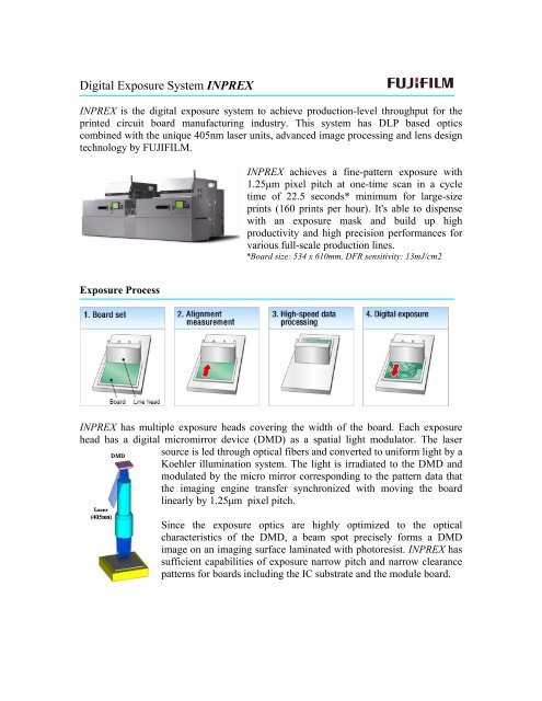
Digital Exposure System <strong>INPREX</strong><br />
<strong>INPREX</strong> is the digital exposure system to achieve production-level throughput for the<br />
printed circuit board manufacturing industry. This system has DLP based optics<br />
combined with the unique 405nm laser units, advanced image processing and lens design<br />
technology <strong>by</strong> <strong>FUJIFILM</strong>.<br />
Exposure Process<br />
<strong>INPREX</strong> achieves a fine-pattern exposure with<br />
1.25μm pixel pitch at one-time scan in a cycle<br />
time of 22.5 seconds* minimum for large-size<br />
prints (160 prints per hour). It's able to dispense<br />
with an exposure mask and build up high<br />
productivity and high precision performances for<br />
various full-scale production lines.<br />
*Board size: 534 x 610mm, DFR sensitivity: 13mJ/cm2<br />
<strong>INPREX</strong> has multiple exposure heads covering the width of the board. Each exposure<br />
head has a digital micromirror device (DMD) as a spatial light modulator. The laser<br />
source is led through optical fibers and converted to uniform light <strong>by</strong> a<br />
Koehler illumination system. The light is irradiated to the DMD and<br />
modulated <strong>by</strong> the micro mirror corresponding to the pattern data that<br />
the imaging engine transfer synchronized with moving the board<br />
linearly <strong>by</strong> 1.25μm pixel pitch.<br />
Since the exposure optics are highly optimized to the optical<br />
characteristics of the DMD, a beam spot precisely forms a DMD<br />
image on an imaging surface laminated with photoresist. <strong>INPREX</strong> has<br />
sufficient capabilities of exposure narrow pitch and narrow clearance<br />
patterns for boards including the IC substrate and the module board.
High-resolution patterns<br />
<strong>FUJIFILM</strong> Corporation<br />
Industrial Digital Imaging<br />
Business Development Office<br />
Tel: +81-3-6271-1087<br />
Corporate Info<br />
http://www.fujifilm.com/about/index.html<br />
<strong>FUJIFILM</strong> Business Products Material Circuit Exposure <strong>INPREX</strong> TOP<br />
http://fujifilm.jp/business/material/circuit/exposure/inprex_en/index.html