IEEE IRPS Douglass - Texas Instruments
IEEE IRPS Douglass - Texas Instruments
IEEE IRPS Douglass - Texas Instruments

You also want an ePaper? Increase the reach of your titles
YUMPU automatically turns print PDFs into web optimized ePapers that Google loves.
Lifetime Estimates and Unique Failure Mechanisms<br />
of the Digital Micromirror Device (DMD)<br />
ABSTRACT<br />
The Digital Micromirror Device TM (DMD TM ) has made great strides<br />
in both performance and reliability. Each device consists of more than<br />
500,000 individually addressable micromirrors. Digital Light<br />
Processing TM technology, based on the DMD, has been used in such<br />
diverse products as projection displays with film-like projected images<br />
and photographic-quality printers. Reliability testing of the DMD<br />
has demonstrated greater than 100,000 operating hours and more than<br />
1 trillion mirror cycles.<br />
This paper discusses DMD reliability development activities; failure<br />
modes investigated (e.g., hinge fatigue, hinge memory, stuck<br />
mirrors, and environmental robustness); various acceleration techniques<br />
(e.g., temperature and duty cycle); corrective actions implemented;<br />
and the resulting evidence that the DMD is exceeding original reliability<br />
goals.<br />
INTRODUCTION<br />
The use of a DMD to digitize light is referred to as Digital Light<br />
Processing TM or DLP TM . A DLP subsystem consists of a light source,<br />
optics, color filters, digital processing and formatting, a DMD, and a<br />
projection lens, as shown in Figure 1. References [1] and [2] describe<br />
DLP in more detail and give additional examples.<br />
The DMD is an array of aluminum micromirrors monolithically<br />
fabricated over an array of SRAM cells. Each SRAM cell corresponds<br />
to a micromirror and allows each mirror to be individually addressed<br />
so as to rotate +10 degrees, limited by a mechanical stop. The<br />
micromirror superstructure is fabricated through a series of aluminum<br />
Digital Processing<br />
and Formatting<br />
DMD<br />
Color Filter<br />
Optics<br />
Projection<br />
Lens<br />
Figure 1. An example of a DLP projection system<br />
using a single DMD<br />
M.R. <strong>Douglass</strong><br />
<strong>Texas</strong> <strong>Instruments</strong>, Digital Imaging<br />
Post Office Box 869305, MS 8477<br />
Plano, <strong>Texas</strong> 75086<br />
972-575-6774; fax: 972-575-0457; e-mail: m-douglass@ti.com<br />
Light Source<br />
Mirror<br />
Spring Tip<br />
Mirror<br />
Address<br />
Electrode<br />
Yoke<br />
Address<br />
Electrode<br />
Bias-Reset<br />
Bus<br />
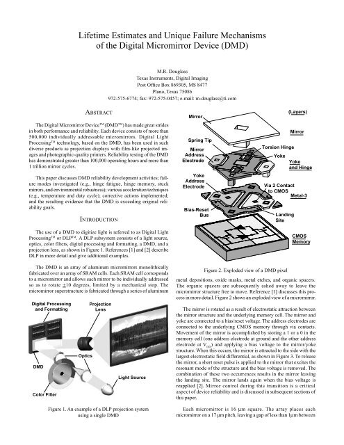
Figure 2. Exploded view of a DMD pixel<br />
Torsion Hinge<br />
Yoke<br />
Yoke<br />
and Hinge<br />
Via 2 Contact<br />
to CMOS<br />
Metal-3<br />
Landing<br />
Site<br />
(Layers)<br />
Mirror<br />
CMOS<br />
Memory<br />
metal depositions, oxide masks, metal etches, and organic spacers.<br />
The organic spacers are subsequently ashed away to leave the<br />
micromirror structure free to move. Reference [1] discusses this process<br />
in more detail. Figure 2 shows an exploded view of a micromirror.<br />
The mirror is rotated as a result of electrostatic attraction between<br />
the mirror structure and the underlying memory cell. The mirror and<br />
yoke are connected to a bias/reset voltage. The address electrodes are<br />
connected to the underlying CMOS memory through via contacts.<br />
Movement of the mirror is accomplished by storing a 1 or a 0 in the<br />
memory cell (one address electrode at ground and the other address<br />
electrode at V DD ) and applying a bias voltage to the mirror/yoke<br />
structure. When this occurs, the mirror is attracted to the side with the<br />
largest electrostatic field differential, as shown in Figure 3. To release<br />
the mirror, a short reset pulse is applied to the mirror that excites the<br />
resonant mode of the structure and the bias voltage is removed. The<br />
combination of these two occurrences results in the mirror leaving<br />
the landing site. The mirror lands again when the bias voltage is<br />
reapplied [2]. Mirror control during this transition is a critical<br />
aspect of device reliability and is discussed in subsequent sections of<br />
this paper.<br />
Each micromirror is 16 μm square. The array places each<br />
micromirror on a 17 μm pitch, leaving a gap of less than 1μm between
Mirror –10 deg<br />
Hinge<br />
Yoke<br />
Spring Tip<br />
Figure 3. Two DMD pixels<br />
the micromirrors. This results in a >90% fill factor and is one significant<br />
advantage of the DMD. The configuration of the array is flexible,<br />
depending on the application. DMD array sizes have been produced<br />
in the following configurations: 840 × 1 (first production DMD used<br />
for low-resolution printing), 640 × 480 (VGA resolution), 848 × 600<br />
(SVGA resolution), 1024 × 768 (XGA resolution), and<br />
1280 × 1024 (SXGA resolution), as well as demonstrations of other<br />
array sizes, such as, 7056 × 64 (high-resolution printing) and<br />
2048 × 1024 (HDTV demonstration for a DARPA contract). Figure 4<br />
is a photograph of a small portion of an array.<br />
DMD RELIABILITY DEVELOPMENT<br />
Mirror +10 deg<br />
Reliability development activities started in early 1992. We began<br />
with a detailed failure modes and effects analysis (FMEA) so that we<br />
could brainstorm potential failure modes and mechanisms. We then<br />
wrote a test plan to verify these failures as well as to highlight any<br />
unanticipated failure modes. We used <strong>Texas</strong> <strong>Instruments</strong> standard semiconductor<br />
qualification test requirements as our baseline, including<br />
applicable tests such as storage life, temperature cycling, thermal shock,<br />
moisture resistance, vibration, wire bond strength, and die shear. The<br />
standard test requirements adequately covered package and die integrity<br />
concerns but did not specifically address microelectromechanical<br />
systems (MEMS) concerns associated with a three-dimensional, moving<br />
integrated circuit.<br />
To address the MEMS aspects of the DMD, the test plan focused<br />
on such obvious potential failure mechanisms as:<br />
• Hinges breaking (fatiguing) over time as a result of routine<br />
operation<br />
• Mirrors breaking as a result of handling (vibration/shock)<br />
• Device lifetime limitations caused by high operating temperatures<br />
• Device lifetime limitations due to intense light exposure.<br />
CMOS<br />
Substrate<br />
We designed a series of tests to address each of these concerns as<br />
well as to try to simulate how a DMD would be used in actual applications.<br />
As our reliability development program progressed, we identified<br />
several acceleration techniques that allowed us to highlight subtle failure<br />
modes and, in turn, implement design improvements much more<br />
rapidly.<br />
As the tests progressed, we soon realized that a DMD is more than<br />
a MEMS device. A DMD has unique optical requirements as well as<br />
chemical properties that offer challenges we did not consider. In other<br />
words, the DMD is a microsystem with mechanical-electrical-opticalchemical<br />
properties that all need to be jointly optimized [3,4].<br />
References [5] and [6] summarize some of the early test results<br />
and potential failure modes. These failure modes and others are discussed<br />
in more detail in the next section.<br />
UNIQUE FAILURE MECHANISMS INVESTIGATED<br />
Hinge Fatigue<br />
Figure 4. Top surface of micromirror array<br />
Hinge fatigue was certainly one of the most significant concerns.<br />
Simple calculations (a mirror switching once every 200 microseconds<br />
for 5 years at 1000 operating hours per year) showed that each mirror<br />
element needed to rotate, or switch, more than 90 × 10 9 times to ensure<br />
a reliable product. Initial finite element analyses using bulk<br />
properties of aluminum highlighted this as a potential concern. A life<br />
test was designed to accelerate the number of mirror cycles per second<br />
by a factor of 10. The test accomplished this by switching the<br />
mirrors more rapidly (once every 20 microseconds) than would occur<br />
during actual operation (a time-based average of 200 to 300 microseconds).<br />
On a small sample, we rapidly exceeded 100 × 10 9 with no<br />
hinge fatigue failures. We increased the sample size and the results<br />
were similarly successful. Several devices also remained on test for<br />
more than 10 12 cycles with no evidence of hinge fatigue.<br />
More recently, we repeated this test on DMDs sampled from the<br />
production flow. Four devices (three with zero defects and one with<br />
one nonfunctional mirror at the start) have been on test for nearly 19,000<br />
hours. Each device has exceeded 1.7 × 10 12 cycles with no evidence of<br />
hinge fatigue. One device has one added defect. After 1.7 × 10 12 cycles,<br />
all functional mirrors were still functional except for the one added<br />
defect, which does not appear to be due to fatigue. Because each DMD<br />
in this test has 307,200 functional mirrors (640 × 480) and each mirror<br />
switched more than 1.7 × 10 12 times, the test has demonstrated more<br />
than 2 × 10 18 total micromirror movements with only one added<br />
micromirror defect and no device failures!<br />
Additional research into why demonstrated hinge lifetimes greatly<br />
exceeded our initial finite element analysis estimates proved that<br />
MEMS models need to use thin-film properties of metal, not bulk properties.<br />
Bulk models of macroscopic fatigue are based on dislocations<br />
coalescing or “piling up” at the surface of the metal. As the density of<br />
the dislocations increases, fatigue cracks form. The dislocations then
accumulate at the fatigue crack, further concentrating mechanical<br />
stresses, until the yield point is exceeded and breakage occurs.<br />
With extremely thin films such as the DMD hinge, the material is<br />
only one grain thick, thus providing two free surfaces to restrain any<br />
dislocations. Because of this, the thin film material does not accumulate<br />
a high enough density of dislocations to form fatigue cracks. In<br />
addition to the test results, hinges from several devices were thoroughly<br />
inspected for fatigue damage using a transmission electron microscope<br />
(TEM). Even at the sections of the hinge where the most stress was<br />
expected, there was no evidence of dislocations, grain irregularity, or<br />
fatigue.<br />
As we refined our finite element analysis models based on thin<br />
film properties and actual test results, we were able to predict the performance<br />
of new designs that matched test results. We now estimate,<br />
as we have demonstrated, that hinges will not break during at least 10<br />
years of normal use in any application and more than 50 years in most<br />
applications. To date, we have not identified the point at which a hinge<br />
wears out.<br />
A significant lesson learned from this potential failure mechanism<br />
is that a thorough understanding of thin film properties as well as models<br />
that support thin film material are critical to successful MEMS development.<br />
Hinge Memory<br />
One of the most significant failure modes identified during our<br />
development program and also one of the last remaining life-limiting<br />
modes is called “hinge memory.” Hinge memory occurs as a mirror is<br />
operated in the same direction for a long period of time. For example,<br />
a mirror continually landed on the off-side (that is, when the mirror<br />
appears dark in a projected image) will exhibit a small amount of residual<br />
tilt when all voltages are removed, as shown in Figure 5.<br />
The mirror will continue to operate properly as long as the electrostatic<br />
fields can direct the mirror to the proper state. When the residual<br />
tilt exceeds approximately 35 to 40% of the 10 degree rotation angle,<br />
most mirrors will not function properly and the pixel will appear non-<br />
Average Number of Nonfunctional Mirrors<br />
1,000,000<br />
100,000<br />
10,000<br />
1,000<br />
100<br />
10<br />
1<br />
0<br />
0 Hours<br />
161 Hours<br />
345 Hours<br />
782 Hours<br />
1150 Hours<br />
Curve A<br />
12 14<br />
16 18<br />
Bias Voltage<br />
ON OFF<br />
Figure 5. A mirror that does not return to a flat position after<br />
electrostatic fields are removed exhibits “hinge memory.”<br />
functional to the observer. Although the address state under the mirror<br />
is changing, when the bias voltage is reapplied to the mirror, the electrostatic<br />
forces on the off-side are greater than those on the on-side<br />
because of the smaller distance. Thus, the mirror will land only to the<br />
off-side.<br />
The factors that contribute to hinge memory consist of operating<br />
temperature and mirror duty cycle. (For hinge memory calculations,<br />
duty cycle is the percentage of time the mirrors are addressed to one<br />
side in relation to the other. For instance, a 95/5 duty cycle means the<br />
mirrors touch the on-side 95% of the time and the off-side 5% of the<br />
time. A duty cycle of 50/50 means the mirrors touch both sides equally<br />
and no hinge memory occurs.)<br />
To evaluate DMD performance, we have developed a measure of<br />
hinge memory using our DMD optical test equipment. The test equipment<br />
sweeps the bias voltage while it counts the number of functional<br />
mirrors at each voltage step. This is referred to as a bias voltage sweep<br />
or V bias curve. Figure 6 shows a series of V bias curves. The Y-axis shows<br />
the number of nonfunctional mirrors; the X-axis shows the bias voltage.<br />
At low bias voltages, mirrors will not land because there are<br />
insufficient electrostatic forces. As the test equipment increases the<br />
bias voltage, more mirrors become functional.<br />
To accelerate hinge memory, we have established a life test using<br />
the standard test conditions of 65 °C and 95/5 duty cycle. As residual<br />
tilt builds up in a DMD, a larger bias voltage is required to land the<br />
mirror on both sides. This is evident in Figure 6. Curve A is the average<br />
V bias curve for a group of DMDs as fabricated. After life testing the<br />
devices at high temperature and high duty cycle, the curve shifts to the<br />
Curve B<br />
20 22 24<br />
Figure 6. Series of bias voltage curves for a group of DMDs. Shifting of these curves is a measure of hinge memory.
Bias Voltage (Average)<br />
22.0<br />
21.0<br />
20.0<br />
19.0<br />
18.0<br />
17.0<br />
16.0<br />
0 200<br />
400 600<br />
Time (Hours)<br />
right, indicating a need for higher bias voltage to maintain mirror functionality.<br />
Curve B is the average V bias curve for the same group of<br />
DMDs after 1150 hours of operation at 65 °C and 95/5 duty cycle.<br />
This series of curves is typical of device performance, and the shape<br />
of the curves is consistent from device to device.<br />
Because the curves are consistent, we can take representative points<br />
and plot their shift in relation to time. Figure 7 shows a plot of V bias,max<br />
(the bias voltage at which the last mirror becomes functional) and V bias,50<br />
(the median of the V bias curve). Notice that both curves are parallel and<br />
that the rate of change is slowing as the test progresses. This, again, is<br />
typical of all DMDs.<br />
Hinge memory on any given device follows a curve similar to that<br />
shown in Figure 7. Several hundred devices were sampled to determine<br />
their behavior over time. We placed each device on a life test at<br />
V bias, Max<br />
V bias, 50<br />
800 1000 1200<br />
Figure 7. Plot of V bias,max and V bias,50 as a function of time. These parametric curves have been used to monitor<br />
process control, implement design improvements, and predict DMD lifetimes<br />
Frequency<br />
50<br />
45<br />
40<br />
35<br />
30<br />
25<br />
20<br />
15<br />
10<br />
5<br />
0<br />
.024 .033 .042 .050 .059 .067 .076 .085 .093 .102 .111 .119 .128 More<br />
Bin(Delta Vb,50 )<br />
100.00%<br />
90.00%<br />
80.00%<br />
70.00%<br />
60.00%<br />
50.00%<br />
40.00%<br />
30.00%<br />
20.00%<br />
10.00%<br />
Figure 8. Distribution of V bias,50 shift after 160 hours of accelerated life test (high temperature and high duty cycle).<br />
This is a statistically normal distribution.<br />
00%<br />
the same test conditions (65 °C, 95/5 duty cycle) and tested them again<br />
after 160 hours. By comparing the V bias,50 before the life test and after<br />
160 hours, we found that the V bias,50 shift is a normal distribution, as<br />
shown in Figure 8. Now that we know this phenomenon is predictable,<br />
we can estimate lifetime by extrapolating time and stress after a<br />
shortened life test. Based on a series of tests with devices operating at<br />
various temperatures and duty cycles, we have determined that temperature<br />
is the dominant factor for hinge memory lifetime. Figure 9<br />
shows projected lifetimes at various temperatures and the performance<br />
improvements achieved since we initiated the reliability development<br />
effort.<br />
The root cause of hinge memory is metal creep of the hinge material.<br />
We evaluated alternate materials and process enhancements to<br />
determine if we could affect hinge memory by reducing metal creep.<br />
Through experimentation and the use of the parametric curves described
Hours<br />
1,000,000<br />
100,000<br />
10,000<br />
1,000<br />
100<br />
10<br />
25<br />
above, we selected an improved hinge material that did not exhibit the<br />
same degree of metal creep. This increased lifetime by a factor of approximately<br />
5 but was still not sufficient for product reliability, since<br />
we estimated a worst-case (65 °C, 95/5 duty cycle) lifetime of only<br />
1000 hours.<br />
The next significant improvement was the implementation of<br />
stepped V DD and a “bipolar reset.” Stepped V DD provides a higher<br />
voltage to the address electrode while the mirror is in transition to the<br />
proper side. Bipolar reset uses a positive bias voltage to land the mirrors<br />
and a negative reset voltage to resonate the mirrors. These two changes<br />
provide a greatly increased electrostatic field differential and allow<br />
the mirrors to be dynamically controlled over a wider range of hinge<br />
memory. As a result of having better control of the mirror during its<br />
transition, DMD lifetime increased by another factor of five to about<br />
5000 hours. At normal DMD operating temperatures of 35 to 45 °C<br />
and a high duty cycle of 95/5, we extrapolate DMD lifetimes of more<br />
than 100,000 hours. At typical duty cycles, such as 85/15 and 75/25,<br />
the lifetime is even higher.<br />
It is evident from this discussion that thermal management is integral<br />
to DMD lifetimes. There are several sources of heat that could<br />
contribute to hinge memory and, therefore, shortened DMD lifetime.<br />
The primary source is radiant energy from the light source. Although,<br />
this would appear to be a significant source of heat, in reality, the<br />
mirror surface reflects most of the energy. Radiant energy striking the<br />
package is much more likely to be absorbed and heat up the entire<br />
package. System apertures and optical integrators are very effective at<br />
reducing the temperature of the DMD package. Since the ceramic package<br />
is an inefficient thermal conductor, most applications attach a<br />
simple heatsink and radiator to the back of the package. This can dissipate<br />
sufficient thermal energy to maintain the DMD at just a few<br />
degrees above its ambient. The second source of thermal energy is<br />
from the projector assembly surrounding the DMD. Significant sources<br />
of heat in a projector include: lamp, lamp ballast, power supply, and<br />
electronics. Efficient and well-designed thermal management is necessary<br />
to ensure that the ambient temperature surrounding the DMD is<br />
maintained at a reasonable level. A third, but insignificant, source of<br />
heat is self-heating of the DMD CMOS.<br />
In most applications developed to date, the DMD operates at<br />
temperatures only 7 to 10 °C above the projector ambient. Thus, even<br />
35<br />
1997 Hinge<br />
1992 Hinge<br />
Normal<br />
Operating<br />
Conditions<br />
Longer DMD lifetime at<br />
less stressful duty cycle<br />
75/25 Duty Cycle<br />
45 55<br />
DMD Operating Temperature (C)<br />
65 75 85<br />
with a projector continuously operating in an ambient temperature of<br />
40 °C, the DMD is operating below 50 °C, thus ensuring a lifetime<br />
greater than 40,000 hours. A thorough discussion of DMD thermal<br />
management techniques can be found in reference [7].<br />
We have recently identified additional improvements to the hinge<br />
material. These changes are expected to further reduce metal creep<br />
and, therefore, increase robustness for operation at high temperature<br />
by at least another order of magnitude. As these improvements are<br />
realized, the resulting reduction in hinge memory can allow more flexibility<br />
in DMD design, DMD control, DMD operating limits, and<br />
system thermal management requirements.<br />
Nonfunctional (Stuck) Mirrors<br />
85/15 Duty Cycle<br />
95/5 Duty Cycle<br />
Figure 9. DMD lifetime estimates when operated at high temperature (65 °C) and high duty cycle<br />
One of the most obvious defects in a DMD array is the appearance<br />
of a nonfunctional mirror. There are numerous potential causes for<br />
improper mirror function. As discussed in the previous section, hinge<br />
memory could eventually result in a mirror appearing to be stuck on<br />
one side or the other. It is still functional, but the electrostatic field is<br />
not sufficient to move the mirror from one side to the other.<br />
Other conditions that contribute to nonfunctional mirrors are particulate<br />
contamination, surface residue, capillary condensation, CMOS<br />
defects, and van der Waals forces.<br />
Most mirror defects in today’s delivered DMDs can be traced to a<br />
particle, either on the surface of the mirror or under the mirror. A particle<br />
in either location, if it is of sufficient size and in a critical location,<br />
can result in improper mirror operation. A particle may be wedged<br />
between mirrors (thus interfering with mirror movement); the particle<br />
may be on the surface of the mirror (thus affecting mirror rotation<br />
dynamics); a particle may have affected the mirror during processing<br />
and damaged a hinge; or a conductive particle can result in a highresistance<br />
short on the address electrode so that the mirror is not<br />
addressed properly. We have observed instances of all these defects<br />
during DMD fabrication.<br />
As in most wafer fabs, particles are the number one contributor to<br />
yield loss, and the DMD is no different. In addition to causing fabrication<br />
yield loss, particles can contribute to reliability failures since the<br />
mirror array is exposed to any loose particles in the package cavity.
Average Number of Nonfunctional Mirrors<br />
100000<br />
10000<br />
1000<br />
100<br />
10<br />
1<br />
0<br />
Curve A<br />
Curve B<br />
0 3 6 9 12 15 18 21 24 27 30 33 36 39<br />
Reset Voltage<br />
Figure 10. V reset curves indicating qualitative measurement<br />
of surface adhesion<br />
Our particle reduction activity is continuously resulting in improved<br />
yields. More importantly, the effort is further reducing our reliability<br />
risk. There are now fewer opportunities for mobile particles that may<br />
eventually result in premature mirror failure or damage.<br />
The second most prevalent cause of nonfunctional mirrors is the<br />
existence of a surface contaminant or residue at the mirror tip landing<br />
point. The contaminant may contribute to increased surface adhesion,<br />
which prevents a mirror from functioning. We observe this occasionally<br />
as a result of improper surface cleaning during the superstructure<br />
processing. Gross processing errors that would result in premature device<br />
failure are readily identified during our normal burn-in and<br />
screening steps. Reliability sample testing identifies more subtle process<br />
variations. Parameters are measured based on a reset voltage sweep<br />
or V reset curve, much the same as the V bias curve discussed in the hinge<br />
memory section of this paper. DMD optical test equipment sweeps the<br />
reset voltage while it counts the number of functional mirrors at each<br />
voltage step. This is referred to as a V reset curve (Figure 10). The Y-axis<br />
shows the number of nonfunctional mirrors; the X-axis shows the reset<br />
voltage. At low reset voltages, mirrors will not release because of<br />
the forces holding the mirrors to the surface. As the reset voltage is<br />
increased, more mirrors release from the surface as the mechanical<br />
energy stored in the mirror overcomes the forces holding the mirror<br />
tips to the landing surface. At even higher reset voltages, energy is<br />
added to the mirror by pulsing it at its resonant frequency.<br />
In this test, we are able to measure the distribution of surface adhesion<br />
across the DMD by reducing the magnitude of the voltage pulse<br />
used to excite the mirror. As the magnitude of the voltage is reduced<br />
from its maximum, any mirrors with excessive surface adhesion cease<br />
to function. As the sweep continues, we can develop a distribution<br />
curve that represents the adhesion signature of each device. Figure 10<br />
provides an example of two curves taken after 160 hours of life test.<br />
Curve A is the distribution of mirrors from a sample of production<br />
DMDs (control devices) and curve B is the distribution of mirrors from<br />
a proposed process change (test devices). It is apparent that the test<br />
devices have a small number of mirrors that exhibit surface adhesion<br />
after the test, whereas the control devices are unchanged. Based on<br />
this information, the test devices were deemed “not as robust” as the<br />
control devices, and the process was further optimized before we in-<br />
Figure 11. Closeup image of a micromirror landing tip showing a<br />
spring tip. The spring not only absorbs energy during landing but<br />
stores energy for more efficient mirror release.<br />
corporated the design change. As a result of monitoring the shift in<br />
this parametric curve over time, we have developed a leading indicator<br />
of potential reliability degradation attributable to excessive surface<br />
adhesion.<br />
Before DMD production was started in 1996, the V reset parametric<br />
curve indicated that surface adhesion was too great to deliver a reliable<br />
device. An innovative approach to overcoming surface adhesion<br />
was the addition of “springs” to the landing tips of the mirrors (Figure<br />
11). As bias is applied to a mirror, the mirror lands, the springs deform,<br />
and energy is stored in the springs. When a reset pulse is applied<br />
and bias voltage is removed, the stored energy pushes the mirror tip<br />
off the surface. This has virtually eliminated the impact of surface<br />
adhesion due to surface contamination.<br />
The remaining three contributors to nonfunctional mirrors, capillary<br />
condensation, CMOS defects, and van der Waals forces are minor<br />
contributors to reliability degradation. We control capillary condensation<br />
by sealing the device in a controlled atmosphere and maintaining<br />
this atmosphere through robust package design methods. Although<br />
CMOS defects are a contributor to yield loss, extensive life testing has<br />
shown no evidence of CMOS parametric degradation contributing to<br />
added defects. Surface adhesion due to van der Waals forces (molecular<br />
surface forces) are minimized by applying a special coating to the<br />
landing surface. The spring tips also provide additional margin against<br />
any increase in surface adhesion forces.<br />
Light Exposure<br />
More than 300 DMDs have been exposed to intense, broad-spectrum<br />
light while operating for more than 1000 hours, with some operating<br />
for well over 5000 hours. Throughout all of these tests, there was no<br />
evidence that light exposure resulted in a fundamental performance<br />
degradation. Many of the devices were tested again after light exposure,<br />
and the reset curves and bias curves (as described previously) were<br />
unchanged from initial outgoing tests. Destructive analyses, such as<br />
residual gas analysis (RGA), X-ray photoelectron spectroscopy (XPS),<br />
and time-of-flight secondary ion mass spectrometry (ToFSIMS), were<br />
also performed on several devices after light exposure. Again, there<br />
was no evidence of fundamental chemical degradation or damage to<br />
the landing surface or superstructure.
Particles |...............................68%<br />
Window Quality |.............18%<br />
Random Pixel |.........10%<br />
Other |...4%<br />
Figure 12. Pareto analysis of DMD field returns<br />
Occasionally we noticed a slight statistical trend toward some<br />
DMDs having more defects when exposed to UV and near-violet light.<br />
There were also several DMDs that failed because of stuck pixels in<br />
preproduction projectors. To better understand this phenomenon, we<br />
ran a series of tests using actual projectors. Each projector was modified<br />
to have a different UV cutoff filter. We found that DMDs were<br />
more likely to fail as a result of nonfunctional stuck pixels if exposed<br />
to light at wavelengths of 400 nm and below. A UV filter was, therefore,<br />
added to the DLP optics path to ensure a flux density of no more<br />
than 0.7 mW/cm 2 below 400 nm, most of which is beyond the visible<br />
spectrum of light. Since the addition of the UV filter, there have been<br />
no reported projector failures.<br />
ENVIRONMENTAL ROBUSTNESS<br />
One of the first steps we performed during the early stages of our<br />
reliability development program was to conduct a series of environmental<br />
tests similar to those performed in accordance with TI<br />
Semiconductor Group standards. These tests consisted of thermal<br />
shock, temperature cycling, moisture exposure, mechanical shock,<br />
vibration, acceleration, temperature storage, altitude, bond wire integrity,<br />
substrate attachment integrity, and ESD characterization. The<br />
superstructure was extremely robust [5]. The mirrors were not damaged<br />
by mechanical shock, vibration, or acceleration. There was no<br />
physical or parametric curve degradation due to temperature shock,<br />
cycling, or storage.<br />
These results, especially the robustness against vibration and shock,<br />
are surprising to some but easily explained. The micromirrors resonate<br />
at frequencies greater than 100 kHz. Normal handling occurs at<br />
frequencies less than 1000 Hz. Thus, the DMD micromirrors are unaffected<br />
by any vibration modes set up during assembly or handling.<br />
Although the mirrors were robust, the tests identified some weaknesses<br />
in the package that were subsequently corrected. The tests also<br />
demonstrated that loose particles in the package cavity can land on<br />
and damage the mirror superstructure. The evidence of mirror damage<br />
due to loose particles was the impetus to accelerate our particle reduction<br />
program to minimize our field reliability risk. The primary source<br />
of particles was found to be from the chemical interaction of the die<br />
attachment adhesive with the coating used to reduce surface adhesion.<br />
The secondary source was silicon particles, mostly from the edge of<br />
the die, and mostly due to the die sawing and separation process. Other<br />
miscellaneous particles (for example, carbon-based and aluminum)<br />
were found to come from handling, assembly, and equipment sources.<br />
Corrective actions to reduce our risk due to particles included the selection<br />
of a new die attachment adhesive, an improved wafer sawing<br />
process, better handling methods, more frequent particle monitoring,<br />
and numerous other process improvements throughout the fabrication<br />
line. Yield loss due to particles has been reduced by a significant percentage<br />
and continues to improve.<br />
LIFETIME DEMONSTRATIONS<br />
AND RELIABILITY ESTIMATES<br />
Through the use of accelerated life testing, the development of rudimentary<br />
models, and environmental qualification, we have identified<br />
what we believe to be the complete list of life-limiting factors. As<br />
discussed previously, hinge fatigue and environmental exposure are<br />
not life limiting. Particulate contamination appears to be random and<br />
not dependent on time or stress. We have not identified any correlation<br />
between light exposure and life. Through design robustness and process<br />
control, we have eliminated all known contributors to surface<br />
adhesion degradation. This leaves hinge memory. Because hinge<br />
memory is so predictable, we have easily estimated our lifetime to be<br />
greater than 100,000 hours, as long as the DMD die temperature is<br />
maintained at 45 °C or below.<br />
Although an actual lifetime of 100,000 hours has not yet been demonstrated,<br />
there is supporting evidence that DMD lifetime is measured<br />
in thousands of hours. Existing data through nearly 2 years of product<br />
deliveries have confirmed no DMD failures due to parametric curve<br />
degradation (bias voltage parametric curves and reset voltage parametric<br />
curves). Several DMDs remain on test through 19,000 actual<br />
operating hours with no failures to date. This certainly supports the<br />
test results and estimates.<br />
In terms of random failures, few devices have failed during enditem<br />
use. We anticipated that particles would dominate random failures,<br />
and that has proved to be true. Particles remain our primary cause of<br />
yield loss, but we have not observed a significant amount of customer<br />
returns caused by particles. In fact, even though particles are our primary<br />
pareto item (Figure 12), the field failure rate for all DMDs<br />
delivered to date is less than 0.2%. We have estimated a mean time<br />
between failures (MTBF) by using the total number of units shipped,<br />
multiplied by an estimate of usage hours per month, divided by the<br />
total number of reported DMD failures. Using conservative estimates<br />
for all three of these factors, we have a demonstrated MTBF (random<br />
failures) of 119,000 hours.<br />
SUMMARY<br />
This paper has highlighted DMD failure modes, failure mechanisms,<br />
and actions taken to improve reliability. Figure 13 presents a summary<br />
of DMD lifetime estimates as a result of major design<br />
enhancements implemented since 1992. The reliability development<br />
program has achieved the following milestones:<br />
• The DMD has been subjected to typical semiconductor environmental<br />
qualification tests and proved to be robust to all,<br />
including temperature cycling, mechanical shock, and vibration.<br />
• We have calculated an MTBF of greater than 119,000 hours<br />
based on actual field data.<br />
• We have projected a lifetime of more than 100,000 hours based<br />
on actual test results and modeling data developed for the DMD.<br />
The only life-limiting failure mechanism identified to date is<br />
temperature-accelerated hinge memory.<br />
• We have demonstrated more than 1.7 × 10¹² mirror cycles with<br />
no hinge fatigue failures. This correlates to 95,000 hours of<br />
normal operation.
Estimated DMD Lifetime<br />
100,000<br />
Hrs<br />
10,000<br />
Hrs<br />
1000<br />
Hrs<br />
100<br />
Hrs<br />
10<br />
Hrs<br />
Range of Performance for<br />
Consumer Applications<br />
Range of Performance for<br />
First-Wave Products<br />
1992 1997<br />
In summary, test results and field performance have demonstrated<br />
that DMD reliability is surpassing its original projections.<br />
ACKNOWLEDGMENTS<br />
The author would like to thank all the members of the <strong>Texas</strong> <strong>Instruments</strong><br />
Digital Imaging Team for their creative and innovative<br />
solutions and their unwavering dedication to reliability. Special recognition<br />
should go to the test development team and the DMD<br />
characterization team, whose contributions helped us gain a more thorough<br />
understanding of the DMD.<br />
REFERENCES<br />
New Hinge<br />
Material<br />
Enhanced<br />
Packaging<br />
[1] L.J. Hornbeck, “Digital Light Processing and MEMS: Timely<br />
Convergence for a Bright Future” (Invited Plenary Paper),<br />
Proceedings SPIE, Vol. 2639, p.2, Micromachining and<br />
Microfabrication Process Technology (1995). Abstract Only.<br />
Color reprint of complete paper available. Call 1-888-DLP-BYTI<br />
(1-888-357-2984).<br />
Improved<br />
Processes<br />
Figure 13. Reliability development and lifetime improvement<br />
Bipolar<br />
Waveforms<br />
With Stepped<br />
V DD<br />
Spring Tip<br />
Superstructure<br />
Innovation<br />
[2] L.J. Hornbeck, “Digital Light Processing for High-Brightness,<br />
High-Resolution Applications” (Invited Paper), Proceedings.<br />
SPIE, Vol. 3013, pp. 27-40, EI ‘97 Projection Displays III (1997).<br />
[3] R.L. Knipe, “Challenges of a Digital Micromirror Device: Modeling<br />
and Design,” SPIE EurOpto Proceedings, Vol. 2783, pp.<br />
135-145 (June 1996).<br />
[4] L.J. Hornbeck, T.R. Howell, R.L. Knipe, and M.A. Mignardi,<br />
“Digital Micromirror Device TM —Commercialization of a Massively<br />
Parallel MEMS Technology,” Microelectronic Systems<br />
1997, DSC-Vol. 62, pp. 3-8, ASME International Mechanical<br />
Engineering Congress and Exposition (1997).<br />
[5] M.R. <strong>Douglass</strong> and D. M. Kozuch, “DMD Reliability Assessment<br />
for Large-Area Displays,” Society for Information Display<br />
International Symposium Digest of Technical Papers, Vol. 26 (Applications<br />
Session A3), pp. 49-52 (May 1995).<br />
[6] M.R. <strong>Douglass</strong> and C. Malemes, “Reliability of Displays Using<br />
Digital Light Processing,” SID ’96, San Diego, CA (May 1996).<br />
[7] J.D. Grimmett, “Thermal Analysis of a Light-Reflecting Digital<br />
Micromirror Device,” International Microelectronics and Packaging<br />
Society, San Diego, CA (Dec 1997).