CF Series - Kyocera
CF Series - Kyocera
CF Series - Kyocera

Create successful ePaper yourself
Turn your PDF publications into a flip-book with our unique Google optimized e-Paper software.
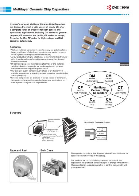
Multilayer Ceramic Chip Capacitors<br />
<strong>Kyocera</strong>'s series of Multilayer Ceramic Chip Capacitors<br />
are designed to meet a wide variety of needs. We offer<br />
a complete range of products for both general and<br />
specialized applications, including CM series for general-<br />
purpose, CT series for low profile, CA series for arrays,<br />
CL series for ICs, <strong>CF</strong> series for high-voltage, and DM<br />
series for automotive.<br />
Features<br />
• We have factories worldwide in order to supply our global customer<br />
bases quickly and efficiently and to maintain our reputation as one<br />
of the highest−volume producers in the industry.<br />
• All our products are highly reliable due to their monolithic structure<br />
of high−purity and superfine uniform ceramics and their integral<br />
internal electrodes.<br />
• By combining superior manufacturing technology and materials<br />
with high dielectric constants, we produce extremely compact<br />
components with exceptional specifications.<br />
• Our stringent quality control in every phase of production from<br />
material procurement to shipping ensures consistent manufacturing<br />
and super quality.<br />
• <strong>Kyocera</strong> components are available in a wide choice of dimensions,<br />
temperature characteristics, rated voltages, and terminations to<br />
meet specific configurational requirements.<br />
Structure<br />
Tape and Reel Bulk Case<br />
External Termination<br />
Electrodes<br />
Internal Electrodes<br />
(Pd, Pd/ Ag or Ni)<br />
Dielectric Ceramic Layer<br />
Temperature compensation: Titanate family<br />
Zirconate family<br />
High dielectric constant:<br />
Barium Titanate family<br />
<strong>CF</strong><br />
series<br />
High-Voltage<br />
DM<br />
series<br />
Automotive<br />
CL<br />
series<br />
ICs<br />
CM<br />
series<br />
General<br />
Multilayer<br />
Ceramic Chip<br />
Capacitors<br />
CA<br />
series<br />
Arrays<br />
Nickel Barrier Termination Products<br />
Ag or Cu or<br />
CuNi<br />
Ni Plating<br />
Sn or Au Plating<br />
RoHS Compliant<br />
CT<br />
series<br />
Low Profile<br />
Please contact your local AVX, <strong>Kyocera</strong> sales office or distributor for<br />
specifications not covered in this catalog.<br />
Our products are continually being improved. As a result, the<br />
capacitance range of each series is subject to change without notice.<br />
Please contact an sales representative to confirm compatibility with<br />
your application.
Multilayer Ceramic Chip Capacitors<br />
<strong>Kyocera</strong> Ceramic Chip Capacitors are available for different applications as classified below:<br />
<strong>Series</strong> Dielectric Options Typical Applications Features Terminations Available Size<br />
CM<br />
CT<br />
CA<br />
C0G (NP0)<br />
X5R<br />
X7R<br />
∗ X6S<br />
∗ X7S<br />
Y5V<br />
X5R<br />
X7R<br />
Y5V<br />
C0G (NP0)<br />
X5R, X7R<br />
CL X7S<br />
<strong>CF</strong><br />
C0G (NP0)<br />
X7R<br />
General purpose Wide cap range Nickel barrier<br />
IC card<br />
(Decoupling)<br />
Digital signal<br />
Pass line<br />
ICs<br />
(Decoupling)<br />
High voltage<br />
&<br />
Power circuits<br />
DM X7R Automotive<br />
∗ Option<br />
∗ Negative temperature coefficient dielectric types are available on request.<br />
Low profile Nickel barrier<br />
Reduction in<br />
placing cost<br />
01005, 0201, 0402<br />
0603, 0805, 1206<br />
1210, 1812<br />
0201, 0402, 0603<br />
0805, 1206, 1210<br />
Nickel barrier 0405, 0508<br />
Low inductance Nickel barrier 0204, 0306<br />
High voltage<br />
250VDC, 630VDC<br />
1000VDC, 2000VDC<br />
3000VDC, 4000VDC<br />
Thermal shock<br />
Resistivity<br />
High reliability<br />
Nickel barrier<br />
0805, 1206, 1210<br />
1812, 2208, 1808<br />
2220<br />
Nickel barrier 0603,0805,1206
Multilayer Ceramic Chip Capacitors<br />
Temperature Characteristics and Tolerance<br />
Temperature Compensation Type<br />
Dielectric C0G (NPO) UΔ (N750)<br />
SL<br />
Value (pF) 0 ppm/ °C −750 ppm/ °C +350 to −1000ppm/ °C<br />
0.5 to 2.7 CK UK SL<br />
3.0 to 3.9 CJ UJ SL<br />
4.0 to 9.0 CH UJ SL<br />
≥10 CG UJ SL<br />
K = ±250ppm/ °C, J = ±120ppm/ °C, H = ±60ppm/ °C, G = ±30ppm/ °C<br />
e.g. CG = 0±30ppm/ °C<br />
Note: All parts of C0G will be marked as “CG” but will conform to the above table.<br />
High Dielectric Constant Type<br />
∗ option<br />
EIA Dielectric Temperature Range ΔC max.<br />
X5R −55 to 85°C<br />
X7R −55 to 125°C<br />
∗X7S −55 to 125°C<br />
∗ X6S −55 to 105°C<br />
±15%<br />
±22%<br />
Y5V −30 to 85°C −82 to +22%<br />
Available Tolerances<br />
Dielectric materials, capacitance values and tolerances are<br />
available in the following combinations only:<br />
EIA Dielectric Tolerance Capacitance<br />
C=±0.25pF<br />
D=±0.50pF<br />
∗1
<strong>CF</strong> <strong>Series</strong><br />
High Voltage Applications<br />
[RoHS Compliant Products]<br />
Features<br />
Perform less than 1 fit failure ratio by high voltage durability and high reliability which has optimized internal electrode structure based on<br />
designing of safety.<br />
Internal structure<br />
Equivalent circuit<br />
General Spec. Mid−voltage range<br />
Straight structure Straight structure Dual cascade Triple cascade<br />
Applications<br />
• Soft modem/ Isolation circuit (Satisfied safety capacitor)<br />
• Camera/ Strobe circuit, Surge Killing, Trigger Circuit<br />
• Mid−voltage range (Straight structure)<br />
Enough break−down voltage margin by taking suitable dielectric<br />
thickness for individual rated voltage.<br />
• Mid−voltage range (Dual cascade structure)<br />
Realize high voltage performance by series connection of two<br />
multilayer capacitor units in a MLCC to divide applied voltage into<br />
two. High durability to surging voltage is guaranteed.<br />
• Mid−voltage range (Triple cascade structure)<br />
Realize high voltage performance by series connection of three<br />
multilayer capacitor units in a MLCC to divide applied voltage into<br />
three. Excellent safety is secured.<br />
The multi cascade structure is a safety design to avoid short circuit<br />
failure.<br />
• LCD Back light Inverter, Ballast Capacitor<br />
• Power Circuit/ DC−DC Converter, Snubber Circuit<br />
Special specification for individual application<br />
A suitable guaranteeing specification will be examined to satisfy customer’s application, such as for AC voltage application.<br />
∗ Information of usage condition will be necessary to be examined.<br />
Custom specification will be available according to your request. Ex. Specification relating to AC voltage.<br />
∗ In-use condition shall be confirmed.<br />
Temperature Compensation Dielectric<br />
Size<br />
(EIA Code)<br />
Temperature<br />
Characteristics<br />
Rated Voltage (VDC)<br />
Capacitance (pF)<br />
R50 0.5<br />
1R0 1.0<br />
1R5 1.5<br />
2.0<br />
3.0<br />
4.0<br />
5.0<br />
6.0<br />
7.0<br />
8.0<br />
9.0<br />
100 10<br />
120<br />
15<br />
22<br />
33<br />
47<br />
68<br />
101 100<br />
121<br />
150<br />
220<br />
330<br />
470<br />
680<br />
<strong>CF</strong>21<br />
(0805)<br />
<strong>CF</strong>316<br />
(1206)<br />
<strong>CF</strong>32<br />
(1210)<br />
<strong>CF</strong>42<br />
(1808)<br />
<strong>CF</strong>43<br />
(1812)<br />
CΔ ∗ CΔ ∗ CΔ ∗ CΔ ∗ CΔ ∗ CΔ ∗<br />
<strong>CF</strong>52<br />
(2208)<br />
250 630 1000 2000 630 1000 2000 1000 2000 3000 1000 2000 3000 4000<br />
D<br />
D D<br />
E E<br />
E<br />
G<br />
102 1000<br />
<br />
E6 <strong>Series</strong><br />
Please contact for capacitance value other than standard.<br />
∗ : CG,CH,CJ,CK<br />
D<br />
E<br />
F<br />
D<br />
F<br />
D<br />
F<br />
A A A<br />
Alphabets in capacitance chart denote dimensions. Please refer to the below table for detail.<br />
Size<br />
Size<br />
Code L<br />
Dimension (mm)<br />
W T<br />
Size<br />
Size<br />
Code L<br />
Dimension (mm)<br />
W T<br />
21<br />
D<br />
E 2.0±0.10 1.25±0.10<br />
0.6±0.10<br />
0.85±0.10<br />
32<br />
D<br />
F<br />
3.2±0.20 2.5±0.20<br />
1.6±0.15<br />
2.0±0.2<br />
G<br />
D<br />
1.25±0.10<br />
1.15±0.10<br />
42<br />
A<br />
B<br />
4.5±0.20 2.0±0.20<br />
1.6 max.<br />
2.2 max.<br />
316 E 3.2±0.20 1.6±0.15 1.25±0.10 43 C 4.5±0.30 3.2±0.20 2.5 max.<br />
F 1.6±0.15 52 A 5.7±0.40 2.0±0.20 2.2 max.<br />
B<br />
B<br />
B<br />
C<br />
C<br />
C<br />
A
Multilayer Ceramic Chip Capacitors<br />
Test Conditions and Standards<br />
Test Conditions and Specifications for Temperature Compensation Type (CΔ to UΔ SL Characteristics)<br />
CM/ CT/ <strong>CF</strong> <strong>Series</strong><br />
Test Items Test Conditions Specifications<br />
Capacitance Value (C) Capacitance Frequency Volt Within tolerance<br />
Q<br />
C≤1000pF<br />
C>1000pF<br />
1MHz±10%<br />
1kHz±10%<br />
0.5 to 5Vrms C≥30pF : Q≥1000<br />
C
Multilayer Ceramic Chip Capacitors<br />
Test Conditions and Standards<br />
Substrate for Electrical Tests (Unit: mm)<br />
<br />
<br />
±<br />
<br />
<br />
<br />
<br />
<br />
<br />
<br />
<br />
<br />
<br />
<br />
<br />
<br />
φ<br />
<br />
<br />
±∗<br />
±<br />
Size<br />
(EIA Code)<br />
a b c<br />
02 (01005) 0.15 0.50 0.20<br />
03 (0201) 0.26 0.92 0.32<br />
05 (0402) 0.4 1.4 0.5<br />
105 (0603) 1.0 3.0 1.2<br />
21 (0805) 1.2 4.0 1.65<br />
316 (1206) 2.2 5.0 2.0<br />
32 (1210) 2.2 5.0 2.9<br />
42 (1808) 3.5 7.0 3.7<br />
43 (1812) 3.5 7.0 3.7<br />
52 (2208) 4.5 8.0 5.6<br />
55 (2220) 4.5 8.0 5.6<br />
Substrate for Bending Test (Unit: mm) Substrate for Adhesion Strength Test<br />
∗ 02, 03, 05 and array: 0.8±0.1mm
Multilayer Ceramic Chip Capacitors<br />
Packaging Options<br />
Tape and Reel<br />
• Reel<br />
F=1mm (02 Type)<br />
B<br />
F<br />
H G<br />
Holes only for plastic carrier tape. 0.3 min.<br />
F=8mm (43, 55 Type)<br />
<br />
F=1mm (02, 03, 05 Type)<br />
F=2mm (03, 05, 105 Type)<br />
A<br />
F=4mm (105, D11, F12, 21, 316, 32, 42, 52 Type)<br />
Feed Hole J<br />
Punched rectangular hole to hold capacitor<br />
Feed Hole J<br />
Punched rectangular hole to hold capacitor<br />
A<br />
A<br />
A<br />
<br />
B<br />
F<br />
<br />
F F<br />
B<br />
Feed Hole<br />
B C<br />
F<br />
H<br />
Holes only for plastic carrier tape. 0.3 min.<br />
<br />
H<br />
R<br />
Punched rectangular<br />
hole to hold<br />
Feed Hole J Parts insertion cavity<br />
<br />
A<br />
Feed Hole J<br />
Punched rectangular hole to hold capacitor<br />
F H<br />
G<br />
E<br />
D<br />
E<br />
C<br />
C<br />
D<br />
<br />
<br />
<br />
E<br />
D<br />
C<br />
E<br />
D<br />
W2<br />
W1<br />
E<br />
(Plastic)<br />
D<br />
C<br />
B<br />
<br />
03 Type: 0.5 max.<br />
05 Type: 0.75 max.<br />
105 Type: 1.1 max.<br />
(Plastic)<br />
2.8 max.<br />
(Plastic)<br />
3.0 max.<br />
0.6 max.<br />
(Paper)<br />
02 Type: 0.4 max.<br />
03 Type: 0.5 max.<br />
05 Type: 0.75 max.<br />
(Paper)<br />
(Paper)<br />
0.6 max. 1.1 max.<br />
Reel (Unit: mm)<br />
Code<br />
Reel<br />
7−inch Reel<br />
(CODE: T, H, Q)<br />
7−inch Reel<br />
(CODE: P)<br />
13−inch Reel<br />
(CODE: L, N, W)<br />
Code<br />
Reel<br />
7−inch Reel<br />
(CODE: T, H, Q)<br />
7−inch Reel<br />
(CODE: P)<br />
13−inch Reel<br />
(CODE: L, N, W)<br />
Carrier Tape (Unit: mm)<br />
Size<br />
(EIA Code)<br />
A B F<br />
02 (01005) ∗<br />
0.23±0.02<br />
0.25±0.03<br />
0.43±0.02<br />
0.45±0.03<br />
1.0±0.02<br />
2.0±0.05<br />
03 (0201) ∗ 0.37±0.03 0.67±0.03<br />
1.0±0.05<br />
2.0±0.05<br />
05 (0402) ∗ 0.65±0.1 1.15±0.1<br />
1.0±0.05<br />
2.0±0.05<br />
105 (0603) 1.0±0.2 1.8±0.2 4.0±0.1<br />
21 (0805) 1.5±0.2 2.3±0.2 4.0±0.1<br />
316 (1206) 2.0±0.2 3.6±0.2 4.0±0.1<br />
32 (1210) 2.9±0.2 3.6±0.2 4.0±0.1<br />
42 (1808) 2.4±0.2 4.9±0.2 4.0±0.1<br />
43 (1812) 3.6±0.2 4.9±0.2 8.0±0.1<br />
52 (2208) 2.4±0.2 6.0±0.2 4.0±0.1<br />
55 (2220) 5.3±0.2 6.0±0.2 8.0±0.1<br />
D11 (0405) 1.15±0.2 1.55±0.2 4.0±0.1<br />
F12 (0508)<br />
∗ Option<br />
1.5±0.2 2.3±0.2 4.0±0.1<br />
(Unit: mm)<br />
F Carrier Tape C D E G H J<br />
1.0<br />
±0.02<br />
4mm<br />
Plastic<br />
4.0<br />
+0.08<br />
1.8<br />
±0.02<br />
0.9<br />
±0.05<br />
−<br />
2.0<br />
±0.04<br />
0.8<br />
±0.04<br />
1.0 1mm 8.0<br />
4.0<br />
±0.05 Paper +0.3/ −0.1<br />
±0.05<br />
2.0<br />
±0.05 8mm<br />
3.5<br />
4.0<br />
±0.1<br />
Paper<br />
8mm<br />
Plastic<br />
8.0<br />
±0.3<br />
±0.05<br />
1.75<br />
±0.1<br />
2.0<br />
±0.05 4.0<br />
±0.1<br />
1.5<br />
+0.1/ −0<br />
8.0<br />
±0.1<br />
12mm<br />
Plastic<br />
A B C D<br />
180 +0<br />
−2.0<br />
178±2.0<br />
330±2.0<br />
12.0<br />
±0.3<br />
φ60 min. 13±0.5 21±0.8<br />
E W1 W2 R<br />
2.0±0.5<br />
10.5±1.5 16.5 max.<br />
4.35±0.3 6.95±1.0<br />
9.5±1.0 16.5 max.<br />
∗ Carrier tape width 8mm.<br />
For size 42 (1808) or over, Tape width 12mm and W1: 14±1.5, W2: 18.4mm max.<br />
5.5<br />
±0.05<br />
1.0
Multilayer Ceramic Chip Capacitors<br />
Surface Mounting Information<br />
Dimensions for recommended typical land<br />
Since the amount of solder (size of fillet) to be used has direct<br />
influence on the capacitor after mounting, the sufficient consideration<br />
is necessary.<br />
When the amounts of solder is too much, the stress that a capacitor<br />
receives becomes larger. It may become the cause of a crack in<br />
the capacitor. When the land design of printed wiring board is<br />
considered, it is necessary to set up the form and size of land pattern<br />
so that the amount of solder is suitable.<br />
(General, High-Voltage, Automotive)<br />
(Arrays)<br />
a<br />
b<br />
a<br />
Design of printed circuit and Soldering<br />
The recommended fillet height shall be 1/2 of the thickness of<br />
capacitors or 0.5mm. When mounting two or more capacitors in the<br />
common land, it is necessary to separate the land with the solder resist<br />
strike so that it may become the exclusive land of each capacitor.<br />
General, High-Voltage (Unit: mm)<br />
Size<br />
(EIA Code)<br />
L×W a b c<br />
02 (01005) 0.4×0.2 0.13 to 0.20 0.12 to 0.18 0.20 to 0.23<br />
03 (0201) 0.6×0.3 0.20 to 0.30 0.25 to 0.35 0.30 to 0.40<br />
05 (0402) 1.0×0.5 0.30 to 0.50 0.35 to 0.45 0.40 to 0.60<br />
105 (0603) 1.6×0.8 0.70 to 1.00 0.80 to 1.00 0.60 to 0.80<br />
21 (0805) 2.0×1.25 1.00 to 1.30 1.00 to 1.20 0.80 to 1.10<br />
316 (1206) 3.2×1.6 2.10 to 2.50 1.10 to 1.30 1.00 to 1.30<br />
32 (1210) 3.2×2.5 2.10 to 2.50 1.10 to 1.30 1.90 to 2.30<br />
42 (1808) 4.5×2.0 2.50 to 3.20 1.80 to 2.30 1.50 to 1.80<br />
43 (1812) 4.5×3.2 2.50 to 3.20 1.80 to 2.30 2.60 to 3.00<br />
52 (2208) 5.7×2.0 4.20 to 4.70 2.00 to 2.50 1.50 to 1.80<br />
55 (2220) 5.7×5.0 4.20 to 4.70 2.00 to 2.50 4.20 to 4.70<br />
Automotive (Unit: mm)<br />
Size<br />
(EIA Code)<br />
L×W a b c<br />
105 (0603) 1.6×0.8 0.60 to 0.90 0.80 to 1.00 0.70 to 1.00<br />
21 (0805) 2.0×1.25 0.90 to 1.20 0.80 to 1.20 0.90 to 1.40<br />
316 (1206) 3.2×1.6 1.40 to 1.90 1.00 to 1.30 1.30 to 1.80<br />
Arrays (Unit: mm)<br />
a b c d<br />
F12 (0508) 0.5 0.5 0.3 0.5<br />
D11 (0405) 0.69 0.28 0.3 0.64<br />
IC (Unit: mm)<br />
Size<br />
(EIA Code)<br />
L×W a b c<br />
05 (0402) 0.5×1.0 0.15 to 0.20 0.20 to 0.30 0.90 to 1.20<br />
105 (0603) 0.8×1.6 0.20 to 0.30 0.30 to 0.50 1.40 to 1.60<br />
Ideal Solder Height<br />
Solder<br />
Chip Capacitor<br />
PCB<br />
T/ 2 or 0.5mm 0.5mm<br />
Item Not recommended example Recommended example/ Separated by solder<br />
Multiple parts mount<br />
Mount with<br />
leaded parts<br />
Wire soldering<br />
after mounting<br />
Overview<br />
F12<br />
Land Pattern<br />
b a<br />
c c c c<br />
d<br />
Sample capacitor<br />
Soldering resist<br />
a<br />
b<br />
a<br />
c<br />
D11<br />
c c<br />
d<br />
Solder resist<br />
Solder resist<br />
Leaded parts Leaded parts<br />
Wire<br />
Soldering iron<br />
Solder resist<br />
Solder resist Solder resist<br />
T T
Multilayer Ceramic Chip Capacitors<br />
Surface Mounting Information<br />
Mounting Design<br />
The chip could crack if the PCB warps during processing after the chip has been soldered.<br />
Recommended chip position on PCB to minimize stress from PCB warpage<br />
(Not recommended) (Ideal)<br />
Actual Mounting<br />
1) If the position of the vacuum nozzle is too low, a large force may be applied to the chip capacitor during mounting, resulting in cracking.<br />
2) During mounting, set the nozzle pressure to a static load of 100 to 300 gf.<br />
3) To minimize the shock of the vaccum nozzle, provide a support pin on the back of the PCB to minimize PCB flexture.<br />
(Not recommended) (Ideal)<br />
Crack<br />
Support pin<br />
4) Bottom position of pick up nozzle should be adjusted to the top surface of a substrate which camber is corrected.<br />
5) To reduce the possibility of chipping and cracks, minimize vibration to chips stored in a bulk case.<br />
6) The discharge pressure must be adjusted to the part size. Verify the pressure during setup to avoid fracturing or cracking the chips capacitors.<br />
Resin Mold<br />
1) If a large amount of resin is used for molding the chip, cracks may occur due to contraction stress during curing. To avoid such cracks, use<br />
a low shrinkage resin.<br />
2) The insulation resistance of the chip will degrade due to moisture absorption. Use a low moisture absorption resin.<br />
3) Check carefully that the resin does not generate a decomposition gas or reaction gas during the curing process or during normal storage.<br />
Such gases may crack the chip capacitor or damage the device itself.
Multilayer Ceramic Chip Capacitors<br />
Precautions<br />
Circuit Design<br />
1. Once application and assembly environments have been checked, the capacitor may be used in conformance with the rating and<br />
performance which are provided in both the catalog and the specifications. Use exceeding that which is specified may result in inferior<br />
performance or cause a short, open, smoking, or flaming to occur, etc.<br />
2. Please consult the manufacturer in advance when the capacitor is used in devices such as: devices which deal with human life, i.e. medical<br />
devices; devices which are highly public orientated; and devices which demand a high standard of liability.<br />
Accident or malfunction of devices such as medical devices, space equipment and devices having to do with atomic power could generate<br />
grave consequence with respect to human lives or, possibly, a portion of the public. Capacitors used in these devices may require high<br />
reliability design different from that of general purpose capacitors.<br />
3. Please use the capacitors in conformance with the operating temperature provided in both the catalog and the specifications.<br />
Be especially cautious not to exceed the maximum temperature. In the situation the maximum temperature set forth in both the catalog and<br />
specifications is exceeded, the capacitor’s insulation resistance may deteriorate, power may suddenly surge and short−circuit may occur.<br />
The capacitor has a loss, and may self−heat due to equivalent series resistance when alternating electric current is passed therethrough. As this<br />
effect becomes especially pronounced in high frequency circuits, please exercise caution.<br />
When using the capacitor in a (self−heating) circuit, please make sure the surface of the capacitor remains under the maximum temperature for<br />
usage. Also, please make certain temperature rises remain below 20°C.<br />
4. Please keep voltage under the rated voltage which is applied to the capacitor. Also, please make certain the peak voltage remains below the<br />
rated voltage when AC voltage is super−imposed to the DC voltage.<br />
In the situation where AC or pulse voltage is employed, ensure average peak voltage does not exceed the rated voltage.<br />
Exceeding the rated voltage provided in both catalog and specifications may lead to defective withstanding voltage or, in worst case<br />
situations, may cause the capacitor to smoke or flame.<br />
5. When the capacitor is to be employed in a circuit in which there is continuous application of a high frequency voltage or a steep pulse<br />
voltage, even though it is within the rated voltage, please inquire to the manufacturer.<br />
In the situation the capacitor is to be employed using a high frequency AC voltage or a extremely fast rising pulse voltage, even though it is<br />
within the rated voltage, it is possible capacitor reliability will deteriorate.<br />
6. It is a common phenomenon of high−dielectric products to have a deteriorated amount of static electricity due to the application of DC voltage.<br />
Due caution is necessary as the degree of deterioration varies depending on the quality of capacitor materials, capacity, as well as the load voltage<br />
at the time of operation.<br />
7. Do not use the capacitor in an environment where it might easily exceed the respective provisions concerning shock and vibration specified<br />
in the catalog and specifications.<br />
In addition, it is a common piezo phenomenon of high dielectric products to have some voltage due to vibration or to have noise due to<br />
voltage change. Please contact sales in such case.<br />
8. If the electrostatic capacity value of the delivered capacitor is within the specified tolerance, please consider this when designing the<br />
respective product in order that the assembled product function appropriately.<br />
9. Please contact us upon using conductive adhesives.<br />
Storage<br />
1. If the component is stored in minimal packaging (a heat−sealed or chuck−type plastic bag), the bag should be kept closed. Once the bag<br />
has been opened, reseal it or store it in a desiccator.<br />
2. Keep storage place temperature +5 to +40 degree C, humidity 20 to 70% RH.<br />
3. The storage atmosphere must be free of gas containing sulfur and chlorine. Also, avoid exposing the product to saline moisture. If the<br />
product is exposed to such atmospheres, the terminals will oxidize and solderability will be effected.<br />
4. Precautions 1) to 3) apply to chip capacitors packaged in carrier tapes and bulk cases.<br />
5. The solderability is assured for 12 months from our shipping date (six months for silver palladium) if the above storage precautions are<br />
followed.<br />
6. Chip capacitors may crack if exposed to hydrogen (H2) gas while sealed or if coated with silicon, which generates hydrogen gas.<br />
Safety application guideline and detailed information of electrical properties are also provided in <strong>Kyocera</strong> home page;<br />
URL: http://www.kyocera.co.jp/electronic/